EP4072010A1 - A linear amplifier for providing a sinusoidal waveform to a load - Google Patents
A linear amplifier for providing a sinusoidal waveform to a load Download PDFInfo
- Publication number
- EP4072010A1 EP4072010A1 EP21305443.0A EP21305443A EP4072010A1 EP 4072010 A1 EP4072010 A1 EP 4072010A1 EP 21305443 A EP21305443 A EP 21305443A EP 4072010 A1 EP4072010 A1 EP 4072010A1
- Authority
- EP
- European Patent Office
- Prior art keywords
- transistor
- linear amplifier
- linear
- state
- amplifier
- Prior art date
- Legal status (The legal status is an assumption and is not a legal conclusion. Google has not performed a legal analysis and makes no representation as to the accuracy of the status listed.)
- Withdrawn
Links
Images


Classifications
-
- H—ELECTRICITY
- H03—ELECTRONIC CIRCUITRY
- H03F—AMPLIFIERS
- H03F1/00—Details of amplifiers with only discharge tubes, only semiconductor devices or only unspecified devices as amplifying elements
- H03F1/32—Modifications of amplifiers to reduce non-linear distortion
- H03F1/3205—Modifications of amplifiers to reduce non-linear distortion in field-effect transistor amplifiers
-
- H—ELECTRICITY
- H03—ELECTRONIC CIRCUITRY
- H03F—AMPLIFIERS
- H03F1/00—Details of amplifiers with only discharge tubes, only semiconductor devices or only unspecified devices as amplifying elements
- H03F1/02—Modifications of amplifiers to raise the efficiency, e.g. gliding Class A stages, use of an auxiliary oscillation
- H03F1/0205—Modifications of amplifiers to raise the efficiency, e.g. gliding Class A stages, use of an auxiliary oscillation in transistor amplifiers
-
- H—ELECTRICITY
- H02—GENERATION; CONVERSION OR DISTRIBUTION OF ELECTRIC POWER
- H02M—APPARATUS FOR CONVERSION BETWEEN AC AND AC, BETWEEN AC AND DC, OR BETWEEN DC AND DC, AND FOR USE WITH MAINS OR SIMILAR POWER SUPPLY SYSTEMS; CONVERSION OF DC OR AC INPUT POWER INTO SURGE OUTPUT POWER; CONTROL OR REGULATION THEREOF
- H02M1/00—Details of apparatus for conversion
- H02M1/0067—Converter structures employing plural converter units, other than for parallel operation of the units on a single load
- H02M1/007—Plural converter units in cascade
-
- H—ELECTRICITY
- H03—ELECTRONIC CIRCUITRY
- H03F—AMPLIFIERS
- H03F1/00—Details of amplifiers with only discharge tubes, only semiconductor devices or only unspecified devices as amplifying elements
- H03F1/02—Modifications of amplifiers to raise the efficiency, e.g. gliding Class A stages, use of an auxiliary oscillation
- H03F1/0205—Modifications of amplifiers to raise the efficiency, e.g. gliding Class A stages, use of an auxiliary oscillation in transistor amplifiers
- H03F1/0211—Modifications of amplifiers to raise the efficiency, e.g. gliding Class A stages, use of an auxiliary oscillation in transistor amplifiers with control of the supply voltage or current
- H03F1/0216—Continuous control
-
- H—ELECTRICITY
- H03—ELECTRONIC CIRCUITRY
- H03F—AMPLIFIERS
- H03F3/00—Amplifiers with only discharge tubes or only semiconductor devices as amplifying elements
- H03F3/20—Power amplifiers, e.g. Class B amplifiers, Class C amplifiers
- H03F3/21—Power amplifiers, e.g. Class B amplifiers, Class C amplifiers with semiconductor devices only
- H03F3/211—Power amplifiers, e.g. Class B amplifiers, Class C amplifiers with semiconductor devices only using a combination of several amplifiers
-
- H—ELECTRICITY
- H03—ELECTRONIC CIRCUITRY
- H03F—AMPLIFIERS
- H03F3/00—Amplifiers with only discharge tubes or only semiconductor devices as amplifying elements
- H03F3/20—Power amplifiers, e.g. Class B amplifiers, Class C amplifiers
- H03F3/24—Power amplifiers, e.g. Class B amplifiers, Class C amplifiers of transmitter output stages
- H03F3/245—Power amplifiers, e.g. Class B amplifiers, Class C amplifiers of transmitter output stages with semiconductor devices only
-
- H—ELECTRICITY
- H02—GENERATION; CONVERSION OR DISTRIBUTION OF ELECTRIC POWER
- H02M—APPARATUS FOR CONVERSION BETWEEN AC AND AC, BETWEEN AC AND DC, OR BETWEEN DC AND DC, AND FOR USE WITH MAINS OR SIMILAR POWER SUPPLY SYSTEMS; CONVERSION OF DC OR AC INPUT POWER INTO SURGE OUTPUT POWER; CONTROL OR REGULATION THEREOF
- H02M7/00—Conversion of AC power input into DC power output; Conversion of DC power input into AC power output
- H02M7/42—Conversion of DC power input into AC power output without possibility of reversal
- H02M7/44—Conversion of DC power input into AC power output without possibility of reversal by static converters
- H02M7/48—Conversion of DC power input into AC power output without possibility of reversal by static converters using discharge tubes with control electrode or semiconductor devices with control electrode
- H02M7/483—Converters with outputs that each can have more than two voltages levels
-
- H—ELECTRICITY
- H02—GENERATION; CONVERSION OR DISTRIBUTION OF ELECTRIC POWER
- H02M—APPARATUS FOR CONVERSION BETWEEN AC AND AC, BETWEEN AC AND DC, OR BETWEEN DC AND DC, AND FOR USE WITH MAINS OR SIMILAR POWER SUPPLY SYSTEMS; CONVERSION OF DC OR AC INPUT POWER INTO SURGE OUTPUT POWER; CONTROL OR REGULATION THEREOF
- H02M7/00—Conversion of AC power input into DC power output; Conversion of DC power input into AC power output
- H02M7/42—Conversion of DC power input into AC power output without possibility of reversal
- H02M7/44—Conversion of DC power input into AC power output without possibility of reversal by static converters
- H02M7/48—Conversion of DC power input into AC power output without possibility of reversal by static converters using discharge tubes with control electrode or semiconductor devices with control electrode
- H02M7/53—Conversion of DC power input into AC power output without possibility of reversal by static converters using discharge tubes with control electrode or semiconductor devices with control electrode using devices of a triode or transistor type requiring continuous application of a control signal
- H02M7/537—Conversion of DC power input into AC power output without possibility of reversal by static converters using discharge tubes with control electrode or semiconductor devices with control electrode using devices of a triode or transistor type requiring continuous application of a control signal using semiconductor devices only, e.g. single switched pulse inverters
- H02M7/5387—Conversion of DC power input into AC power output without possibility of reversal by static converters using discharge tubes with control electrode or semiconductor devices with control electrode using devices of a triode or transistor type requiring continuous application of a control signal using semiconductor devices only, e.g. single switched pulse inverters in a bridge configuration
Definitions
- the present invention relates generally to a linear amplifier for providing a sinusoidal waveform to a load.
- Linear mode application is commonly used for power as well as radiofrequency applications for the amplification of sinusoidal signals or for direct current control.
- the linear mode is used for fan application or battery charging where a power semiconductor is used as a current source directly controlled through its gate.
- the so-called “class-A” or “class-B” linear amplifier essentially produces a continuous sinusoidal voltage and/or current, while a pulse width modulation (PWM) inverter applies a discrete voltage-pulse train to the load.
- PWM pulse width modulation
- the linear amplifier goes along a significant amount of power losses, because the semiconductor devices always work in linear amplification state (thus the transistor is crossed by a current and a voltage). Therefore, the efficiency which is around 78.5% of the linear amplifier (which is around 78.5%) is rather low, that even the conventional class-B amplifier.
- the Class B or "Push-Pull" linear power amplifier is using complementary pair of switch P and N in order to produce a symmetrical sinusoidal waveform.
- the present invention aims to propose a new topology of circuit with only N-type semiconductors with a reduced number of components and a higher efficiency.
- the present invention concerns a linear amplifier for providing a sinusoidal waveform to a load, characterised in that the linear amplifier is composed of an asymmetric amplifier and a H-bridge module, the asymmetric amplifier comprises at least one transistor that amplifies a full wave rectified sinus signal that is transformed by the H bridge module into a sinewave signal that is provided to the load.
- the asymmetric amplifier comprises plural transistors of the same type, and the same full wave rectified sinus signal is provided to each transistor.
- the transistors are N type semiconductors.
- each transistor is in a OFF state or in a linear amplification state or in a ON state and only one transistor among the plural transistors is in the linear amplification state during at least one period of time of the period of the full rectified wave signal.
- the duration of the linear amplification state of the transistors is reduced, less stress is then supported by the transistors.
- the asymmetric amplifier comprises the same number of DC voltage sources as the number of transistors.
- the duration of the linear amplification state of the transistors may be controlled easily.
- each voltage source provides the same voltage value.
- the semiconductors have the same breakdown voltage, leading to easy semiconductor choice and cost reduction for mass production of the asymmetric linear amplifier.
- the semiconductors have the same breakdown voltage, leading to easy semiconductor choice and cost reduction for mass production of the asymmetric linear amplifier.
- Fig. 1 represents an example of architecture of linear amplifier according to the present invention.
- the linear amplifier is, according to the present invention, composed of an asymmetric linear amplifier 10 and a H-bridge module 15.
- the asymmetric linear amplifier 10 is composed of at least one transistor the gate of which is driven by a positive full wave rectified sinus signal.
- the asymmetric linear amplifier 10 comprises for transistors Tr1, Tr2, Tr3 and T4, three diodes D1, D2 and D3 and four DC voltage sources V1, V2, V3 and V4.
- the transistors are for example N type MOSFET transistors.
- the same signal Vin applied to each gate of the transistors Tr1 to Tr4 is a positive full wave rectified sinus signal.
- the drain of the transistor Tr1 is connected to a first terminal of the DC voltage source V1.
- the source of the transistor Tr1 is connected to a cathode of the diode D1, the anode of which is connected to a second terminal of the DC voltage source V1 and to a first terminal of the DC voltage source V2.
- the voltage between the second terminal of the DC voltage source V1 and the first terminal of the DC voltage source V1 is positive.
- the drain of the transistor Tr2 is connected to the source of the transistor Tr1 and to the cathode of the diode D1.
- the source of the transistor Tr2 is connected to a cathode of the diode D2, the anode of which is connected to a second terminal of the DC voltage source V2 and to a first terminal of the DC voltage source V3.
- the voltage between the second terminal of the DC voltage source V2 and the first terminal of the DC voltage source V2 is positive.
- the drain of the transistor Tr3 is connected to the source of the transistor Tr2 and to the cathode of the diode D2.
- the source of the transistor Tr3 is connected to a cathode of the diode D3, the anode of which is connected to a second terminal of the DC voltage source V3 and to a first terminal of the DC voltage source V4.
- the voltage between the second terminal of the DC voltage source V3 and the first terminal of the DC voltage source V3 is positive.
- the drain of the transistor Tr4 is connected to the source of the transistor T3 and to the cathode of the diode D3.
- the source of the transistor Tr4 is connected to a first terminal of the H-bridge module 15.
- the second terminal of the DC voltage source V4 is connected to a second terminal of the H-bridge module 15 and to the ground.
- the voltage between the second terminal of the DC voltage source V4 and the first terminal of the DC voltage source V3 is positive.
- each DC voltage source V1 to V4 is identical and equal to Vdc/4, where Vdc is for example equal to 300 Volts.
- each DC voltage source V1 to V4 is different.
- the H bridge module 15 is composed of fourth switches S1, S2, S3 and S4.
- a first terminal of the switch S1 is connected to the first terminal of the H bridge module 15, a first terminal of the switch S3 is connected to the first terminal of the H bridge module 15.
- a second terminal of the switch S1 is connected to a first terminal of the switch S2 and to a first terminal of the load Lo.
- a second terminal of the switch S3 is connected to a first terminal of the switch S4 and to a second terminal of the load Lo.
- the second terminal of the switch S2 is connected to the second terminal of the H bridge module 15.
- the second terminal of the switch S4 is connected to the second terminal of the H bridge module 15.
- the load Lo is for example a power grid and the linear amplifier provides a sinewave current to the power grid by providing a full wave rectified sinus current lamp that is unfolded by the H bridge module in order to provide the sinewave current to the power grid.
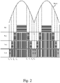
- Fig. 2 represents chronograms of the different operation modes of the power semiconductors of the asymmetric linear amplifier.
- the voltage Vamp is the voltage between the first and second terminals of the H bridge module 15.
- the transistors Tr1 to Tr4 are in a OFF state or in ON state or in a linear amplification state.
- the linear amplification state is represented in Fig. 2 by an area of horizontal lines, the ON state is represented by an area of vertical lines.
- the transistor Tr4 is in the linear amplification state and the transistors Tr1 to Tr3 are in the OFF state.
- the transistor Tr4 is in the ON state, the transistor Tr3 is in the linear amplification state and the transistors Tr2 and Tr1 are in the OFF state.
- the transistors Tr3 and Tr4 are in the ON state, the transistor Tr2 is in the linear amplification state and the transistor Tr1 is in the OFF state.
- the transistors Tr2, Tr3 and Tr4 are in the ON state and the transistor Tr1 is in the linear amplification state.
- the transistors Tr3 and Tr4 are in the ON state, the transistor Tr2 is in the linear amplification state and the transistor Tr1 is in the OFF state.
- the transistor Tr4 is in the ON state, the transistor Tr3 is in the linear amplification state and the transistors Tr2 and Tr1 are in the OFF state.
- the transistor Tr4 is in the linear amplification state and the transistors Tr1 to Tr3 are in the OFF state.
- linear amplification state may be named also saturation state
- ON state may be named also ohmic state
- Fig. 3 represents the different waveforms of signals of the asymmetric linear amplifier according to the present invention.
- the signal Vlo is the voltage on the load Lo.
- Fig. 4 represents the waveforms for controlling the semiconductors of the H bridge module of the linear amplifier.
- Fig. 4 the voltage Vlo, the command signal S1-S4 applied to the switches S1 and S4 and the command signal S2-S3 applied to the switches S2 and S3 are shown.
Landscapes
- Engineering & Computer Science (AREA)
- Power Engineering (AREA)
- Physics & Mathematics (AREA)
- Nonlinear Science (AREA)
- Amplifiers (AREA)
Abstract
Description
- The present invention relates generally to a linear amplifier for providing a sinusoidal waveform to a load.
- Linear mode application is commonly used for power as well as radiofrequency applications for the amplification of sinusoidal signals or for direct current control.
- In power electronics applications, the linear mode is used for fan application or battery charging where a power semiconductor is used as a current source directly controlled through its gate.
- On the other hand, the so-called "class-A" or "class-B" linear amplifier essentially produces a continuous sinusoidal voltage and/or current, while a pulse width modulation (PWM) inverter applies a discrete voltage-pulse train to the load.
- The linear amplifier goes along a significant amount of power losses, because the semiconductor devices always work in linear amplification state (thus the transistor is crossed by a current and a voltage). Therefore, the efficiency which is around 78.5% of the linear amplifier (which is around 78.5%) is rather low, that even the conventional class-B amplifier.
- The Class B or "Push-Pull" linear power amplifier is using complementary pair of switch P and N in order to produce a symmetrical sinusoidal waveform.
- Different kinds of improvement have been published for dealing with the low efficiency of this basic class B cell, like for example by multiplying the number of stages in order to reduce the constraints on each switch stage. The improvement consisting in increasing the number of stages remains capped by the cost and the complexity of the circuit.
- As explained in the above paragraph, for high efficiency amplifier, a high number of stages is needed, which means a high number of P and N semiconductors as well as high complexity of the circuit. In terms of manufacturing, P semiconductors are not as largely used as the N type which means the availability for P type semiconductors is more difficult and with less variety.
- The present invention aims to propose a new topology of circuit with only N-type semiconductors with a reduced number of components and a higher efficiency.
- To that end, the present invention concerns a linear amplifier for providing a sinusoidal waveform to a load, characterised in that the linear amplifier is composed of an asymmetric amplifier and a H-bridge module, the asymmetric amplifier comprises at least one transistor that amplifies a full wave rectified sinus signal that is transformed by the H bridge module into a sinewave signal that is provided to the load.
- Thus, only semiconductors of the same type may be used, the number of components is reduced and a higher efficiency is obtained.
- According to a particular feature, the asymmetric amplifier comprises plural transistors of the same type, and the same full wave rectified sinus signal is provided to each transistor.
- Thus, the efficiency of the linear amplifier is improved.
- According to a particular feature, the transistors are N type semiconductors.
- Thus, the choice of semiconductors is improved and the cost of the linear amplifier is reduced.
- According to a particular feature, each transistor is in a OFF state or in a linear amplification state or in a ON state and only one transistor among the plural transistors is in the linear amplification state during at least one period of time of the period of the full rectified wave signal.
- Thus, the duration of the linear amplification state of the transistors is reduced, less stress is then supported by the transistors.
- According to a particular feature, the asymmetric amplifier comprises the same number of DC voltage sources as the number of transistors.
- Thus, the duration of the linear amplification state of the transistors may be controlled easily.
- According to a particular feature, each voltage source provides the same voltage value.
- Thus, the semiconductors have the same breakdown voltage, leading to easy semiconductor choice and cost reduction for mass production of the asymmetric linear amplifier.
- Thus, the semiconductors have the same breakdown voltage, leading to easy semiconductor choice and cost reduction for mass production of the asymmetric linear amplifier.
- The characteristics of the invention will emerge more clearly from a reading of the following description of example embodiments, the said description being produced with reference to the accompanying drawings, among which:
-
Fig. 1 represents an example of architecture of linear amplifier according to the present invention; -
Fig. 2 represents chronograms of the different operation modes of the power semiconductors of the asymmetric linear amplifier; -
Fig. 3 represents the different waveforms of signals of the asymmetric linear amplifier according to the present invention; -
Fig. 4 represents the waveforms for controlling the semiconductors of the H bridge module of the linear amplifier. -
Fig. 1 represents an example of architecture of linear amplifier according to the present invention. - The linear amplifier is, according to the present invention, composed of an asymmetric
linear amplifier 10 and a H-bridge module 15. - The asymmetric
linear amplifier 10 is composed of at least one transistor the gate of which is driven by a positive full wave rectified sinus signal. In the example ofFig. 1 , the asymmetriclinear amplifier 10 comprises for transistors Tr1, Tr2, Tr3 and T4, three diodes D1, D2 and D3 and four DC voltage sources V1, V2, V3 and V4. - Less or more transistors may be used in the asymmetric linear amplifier.
- The transistors are for example N type MOSFET transistors.
- The same signal Vin applied to each gate of the transistors Tr1 to Tr4 is a positive full wave rectified sinus signal.
- The drain of the transistor Tr1 is connected to a first terminal of the DC voltage source V1.
- The source of the transistor Tr1 is connected to a cathode of the diode D1, the anode of which is connected to a second terminal of the DC voltage source V1 and to a first terminal of the DC voltage source V2.
- The voltage between the second terminal of the DC voltage source V1 and the first terminal of the DC voltage source V1 is positive.
- The drain of the transistor Tr2 is connected to the source of the transistor Tr1 and to the cathode of the diode D1.
- The source of the transistor Tr2 is connected to a cathode of the diode D2, the anode of which is connected to a second terminal of the DC voltage source V2 and to a first terminal of the DC voltage source V3.
- The voltage between the second terminal of the DC voltage source V2 and the first terminal of the DC voltage source V2 is positive.
- The drain of the transistor Tr3 is connected to the source of the transistor Tr2 and to the cathode of the diode D2.
- The source of the transistor Tr3 is connected to a cathode of the diode D3, the anode of which is connected to a second terminal of the DC voltage source V3 and to a first terminal of the DC voltage source V4.
- The voltage between the second terminal of the DC voltage source V3 and the first terminal of the DC voltage source V3 is positive.
- The drain of the transistor Tr4 is connected to the source of the transistor T3 and to the cathode of the diode D3.
- The source of the transistor Tr4 is connected to a first terminal of the H-
bridge module 15. - The second terminal of the DC voltage source V4 is connected to a second terminal of the H-
bridge module 15 and to the ground. - The voltage between the second terminal of the DC voltage source V4 and the first terminal of the DC voltage source V3 is positive.
- Preferably, the voltage provided by each DC voltage source V1 to V4 is identical and equal to Vdc/4, where Vdc is for example equal to 300 Volts.
- In a variant, the voltage provided by each DC voltage source V1 to V4 is different.
- The
H bridge module 15 is composed of fourth switches S1, S2, S3 and S4. - A first terminal of the switch S1 is connected to the first terminal of the
H bridge module 15, a first terminal of the switch S3 is connected to the first terminal of theH bridge module 15. - A second terminal of the switch S1 is connected to a first terminal of the switch S2 and to a first terminal of the load Lo. A second terminal of the switch S3 is connected to a first terminal of the switch S4 and to a second terminal of the load Lo.
- The second terminal of the switch S2 is connected to the second terminal of the
H bridge module 15. The second terminal of the switch S4 is connected to the second terminal of theH bridge module 15. - The load Lo is for example a power grid and the linear amplifier provides a sinewave current to the power grid by providing a full wave rectified sinus current lamp that is unfolded by the H bridge module in order to provide the sinewave current to the power grid.
-
Fig. 2 represents chronograms of the different operation modes of the power semiconductors of the asymmetric linear amplifier. - The voltage Vamp is the voltage between the first and second terminals of the
H bridge module 15. - The transistors Tr1 to Tr4 are in a OFF state or in ON state or in a linear amplification state.
- The linear amplification state is represented in
Fig. 2 by an area of horizontal lines, the ON state is represented by an area of vertical lines. - Between times to and t1, the transistor Tr4 is in the linear amplification state and the transistors Tr1 to Tr3 are in the OFF state.
- Between times t1 and t2, the transistor Tr4 is in the ON state, the transistor Tr3 is in the linear amplification state and the transistors Tr2 and Tr1 are in the OFF state.
- Between times t2 and t3, the transistors Tr3 and Tr4 are in the ON state, the transistor Tr2 is in the linear amplification state and the transistor Tr1 is in the OFF state.
- Between times t3 and t4, the transistors Tr2, Tr3 and Tr4 are in the ON state and the transistor Tr1 is in the linear amplification state.
- Between times t4 and t5, the transistors Tr3 and Tr4 are in the ON state, the transistor Tr2 is in the linear amplification state and the transistor Tr1 is in the OFF state.
- Between times t5 and t6, the transistor Tr4 is in the ON state, the transistor Tr3 is in the linear amplification state and the transistors Tr2 and Tr1 are in the OFF state.
- Between times t6 and t7, the transistor Tr4 is in the linear amplification state and the transistors Tr1 to Tr3 are in the OFF state.
- It has to be noted here that the linear amplification state may be named also saturation state, the ON state may be named also ohmic state.
-
Fig. 3 represents the different waveforms of signals of the asymmetric linear amplifier according to the present invention. - In
Fig. 3 , the signals Vin, Vamp, lamp and Vlo are shown. - The signal Vlo is the voltage on the load Lo.
-
Fig. 4 represents the waveforms for controlling the semiconductors of the H bridge module of the linear amplifier. - In
Fig. 4 , the voltage Vlo, the command signal S1-S4 applied to the switches S1 and S4 and the command signal S2-S3 applied to the switches S2 and S3 are shown. - When the voltage Vlo is positive, the command signal S1-S4 is high and the switches S1 and S4 are conducting.
- When the voltage Vlo is positive, the command signal S2-S4 is low and the switches S2 and S3 are not conducting.
- When the voltage Vlo is negative, the command signal S1-S4 is low and the switches S1 and S4 are not conducting.
- When the voltage Vlo is negative, the command signal S2-S4 is high and the switches S2 and S3 are conducting.
- Naturally, many modifications can be made to the embodiments of the invention described above without departing from the scope of the present invention.
Claims (6)
- A linear amplifier for providing a sinusoidal waveform to a load, characterised in that the linear amplifier is composed of an asymmetric amplifier and a H-bridge module, the asymmetric amplifier comprises at least one transistor that amplifies a full wave rectified sinus signal that is transformed by the H bridge module into a sinewave signal that is provided to the load.
- The linear amplifier according to claim 1, characterized in that the asymmetric amplifier comprises plural transistors of the same type, and the same full wave rectified sinus signal is provided to each transistor.
- The linear amplifier according to claim 2, characterized in that the transistors are N type semiconductors.
- The linear amplifier according to claim 2 or 3, characterized in that each transistor is in a OFF state or in a linear amplification state or in a ON state and only one transistor among the plural transistors is in the linear amplification state during at least one period of time of the period of the full wave rectified sinus signal.
- The linear amplifier according to claim 4, characterized in that the asymmetric amplifier comprises the same number of DC voltage sources as the number of transistors.
- The linear amplifier according to claim 5, characterized in that each voltage source provides the same voltage value.
Priority Applications (5)
| Application Number | Priority Date | Filing Date | Title |
|---|---|---|---|
| EP21305443.0A EP4072010A1 (en) | 2021-04-07 | 2021-04-07 | A linear amplifier for providing a sinusoidal waveform to a load |
| US18/280,822 US20240154577A1 (en) | 2021-04-07 | 2021-08-26 | Linear amplifier for providing sinusoidal waveform to load |
| PCT/JP2021/032211 WO2022215285A1 (en) | 2021-04-07 | 2021-08-26 | Linear amplifier for providing sinusoidal waveform to load |
| CN202180096133.1A CN117121371A (en) | 2021-04-07 | 2021-08-26 | Linear amplifier for delivering sinusoidal waveforms to loads |
| JP2023563361A JP2024501586A (en) | 2021-04-07 | 2021-08-26 | Linear amplifier that provides a sinusoidal waveform to the load |
Applications Claiming Priority (1)
| Application Number | Priority Date | Filing Date | Title |
|---|---|---|---|
| EP21305443.0A EP4072010A1 (en) | 2021-04-07 | 2021-04-07 | A linear amplifier for providing a sinusoidal waveform to a load |
Publications (1)
| Publication Number | Publication Date |
|---|---|
| EP4072010A1 true EP4072010A1 (en) | 2022-10-12 |
Family
ID=75588169
Family Applications (1)
| Application Number | Title | Priority Date | Filing Date |
|---|---|---|---|
| EP21305443.0A Withdrawn EP4072010A1 (en) | 2021-04-07 | 2021-04-07 | A linear amplifier for providing a sinusoidal waveform to a load |
Country Status (5)
| Country | Link |
|---|---|
| US (1) | US20240154577A1 (en) |
| EP (1) | EP4072010A1 (en) |
| JP (1) | JP2024501586A (en) |
| CN (1) | CN117121371A (en) |
| WO (1) | WO2022215285A1 (en) |
Family Cites Families (1)
| Publication number | Priority date | Publication date | Assignee | Title |
|---|---|---|---|---|
| EP2764604B1 (en) * | 2011-08-04 | 2018-07-04 | WiTricity Corporation | Tunable wireless power architectures |
-
2021
- 2021-04-07 EP EP21305443.0A patent/EP4072010A1/en not_active Withdrawn
- 2021-08-26 JP JP2023563361A patent/JP2024501586A/en not_active Withdrawn
- 2021-08-26 CN CN202180096133.1A patent/CN117121371A/en active Pending
- 2021-08-26 WO PCT/JP2021/032211 patent/WO2022215285A1/en not_active Ceased
- 2021-08-26 US US18/280,822 patent/US20240154577A1/en active Pending
Non-Patent Citations (3)
| Title |
|---|
| AL-JUDI ARIF ET AL: "Cascading of diode bypassed transistor-voltage-source units in multilevel inverters", IET POWER ELECTRONICS, IET, UK, vol. 6, no. 3, 1 March 2013 (2013-03-01), pages 554 - 560, XP006046004, ISSN: 1755-4535, DOI: 10.1049/IET-PEL.2011.0499 * |
| OOTA M ET AL: "Development of Switched-Capacitor bi-directional DC-AC converter for inductive and capacitive loads", INDUSTRIAL ELECTRONICS, 2009. ISIE 2009. IEEE INTERNATIONAL SYMPOSIUM ON, IEEE, PISCATAWAY, NJ, USA, 5 July 2009 (2009-07-05), pages 1618 - 1623, XP031519153, ISBN: 978-1-4244-4347-5 * |
| SU G-J: "Multilevel DC-Link Inverter", IEEE TRANSACTIONS ON INDUSTRY APPLICATIONS, IEEE SERVICE CENTER, PISCATAWAY, NJ, US, vol. 41, no. 3, 1 May 2005 (2005-05-01), pages 848 - 854, XP011132530, ISSN: 0093-9994, DOI: 10.1109/TIA.2005.847306 * |
Also Published As
| Publication number | Publication date |
|---|---|
| WO2022215285A1 (en) | 2022-10-13 |
| US20240154577A1 (en) | 2024-05-09 |
| JP2024501586A (en) | 2024-01-12 |
| CN117121371A (en) | 2023-11-24 |
Similar Documents
| Publication | Publication Date | Title |
|---|---|---|
| US9502973B2 (en) | Buck converter with III-nitride switch for substantially increased input-to-output voltage ratio | |
| US5107151A (en) | Switching circuit employing electronic devices in series with an inductor to avoid commutation breakdown and extending the current range of switching circuits by using igbt devices in place of mosfets | |
| JP6008330B2 (en) | Power converter | |
| US10256736B2 (en) | DC-DC converter with polarity reversal protection | |
| EP2040365B1 (en) | Forward converter with self-driven synchronous rectifiers | |
| AU2017394665A1 (en) | Transformer based gate drive circuit | |
| TWI532306B (en) | Inverter circuit, power converter circuit, and electric vehicle | |
| CN210469160U (en) | Novel water pump motor control circuit | |
| US20230049948A1 (en) | Bi-Directional Medium Voltage Converter | |
| CN112737343A (en) | Control method of full-bridge LLC circuit and full-bridge LLC resonance transformation device | |
| CN113241942B (en) | A Bootstrap Drive Circuit Applied to Four-Switch Buck-Boost Converter | |
| US20220140748A1 (en) | Semiconductor device and inverter device | |
| WO2003096525B1 (en) | Polyphase impedance transformation amplifier | |
| US11128216B2 (en) | Converter, step-down method based on the converter and electronic device | |
| US20240154577A1 (en) | Linear amplifier for providing sinusoidal waveform to load | |
| US6867574B2 (en) | Switch mode power supply and driving method for efficient RF amplification | |
| JP3802678B2 (en) | Control method of step-down chopper type DC-DC converter | |
| US7729133B2 (en) | Secondary side-driven half-bridge power supply | |
| CN212588264U (en) | Power driving circuit based on MOSFET | |
| KR101969117B1 (en) | Active Clamp Forward Converter And Method Of Driving The Same | |
| AU2006219967A1 (en) | Transistor arrangement for rectifier and inverter | |
| CN114759791A (en) | High-reliability converter and control method | |
| JPH07298633A (en) | 3-phase PWM inverter | |
| CN220528018U (en) | IGBT drive detection protection circuit and IGBT drive device | |
| JPH0740785B2 (en) | Multi-channel inverter circuit |
Legal Events
| Date | Code | Title | Description |
|---|---|---|---|
| PUAI | Public reference made under article 153(3) epc to a published international application that has entered the european phase |
Free format text: ORIGINAL CODE: 0009012 |
|
| STAA | Information on the status of an ep patent application or granted ep patent |
Free format text: STATUS: THE APPLICATION HAS BEEN PUBLISHED |
|
| AK | Designated contracting states |
Kind code of ref document: A1 Designated state(s): AL AT BE BG CH CY CZ DE DK EE ES FI FR GB GR HR HU IE IS IT LI LT LU LV MC MK MT NL NO PL PT RO RS SE SI SK SM TR |
|
| STAA | Information on the status of an ep patent application or granted ep patent |
Free format text: STATUS: REQUEST FOR EXAMINATION WAS MADE |
|
| 17P | Request for examination filed |
Effective date: 20230407 |
|
| RBV | Designated contracting states (corrected) |
Designated state(s): AL AT BE BG CH CY CZ DE DK EE ES FI FR GB GR HR HU IE IS IT LI LT LU LV MC MK MT NL NO PL PT RO RS SE SI SK SM TR |
|
| STAA | Information on the status of an ep patent application or granted ep patent |
Free format text: STATUS: THE APPLICATION IS DEEMED TO BE WITHDRAWN |
|
| 18D | Application deemed to be withdrawn |
Effective date: 20241101 |