US7729133B2 - Secondary side-driven half-bridge power supply - Google Patents
Secondary side-driven half-bridge power supply Download PDFInfo
- Publication number
- US7729133B2 US7729133B2 US11/964,662 US96466207A US7729133B2 US 7729133 B2 US7729133 B2 US 7729133B2 US 96466207 A US96466207 A US 96466207A US 7729133 B2 US7729133 B2 US 7729133B2
- Authority
- US
- United States
- Prior art keywords
- secondary side
- power supply
- bridge
- mosfet unit
- bridge power
- Prior art date
- Legal status (The legal status is an assumption and is not a legal conclusion. Google has not performed a legal analysis and makes no representation as to the accuracy of the status listed.)
- Expired - Fee Related, expires
Links
Images


Classifications
-
- H—ELECTRICITY
- H02—GENERATION; CONVERSION OR DISTRIBUTION OF ELECTRIC POWER
- H02M—APPARATUS FOR CONVERSION BETWEEN AC AND AC, BETWEEN AC AND DC, OR BETWEEN DC AND DC, AND FOR USE WITH MAINS OR SIMILAR POWER SUPPLY SYSTEMS; CONVERSION OF DC OR AC INPUT POWER INTO SURGE OUTPUT POWER; CONTROL OR REGULATION THEREOF
- H02M1/00—Details of apparatus for conversion
- H02M1/08—Circuits specially adapted for the generation of control voltages for semiconductor devices incorporated in static converters
-
- H—ELECTRICITY
- H02—GENERATION; CONVERSION OR DISTRIBUTION OF ELECTRIC POWER
- H02M—APPARATUS FOR CONVERSION BETWEEN AC AND AC, BETWEEN AC AND DC, OR BETWEEN DC AND DC, AND FOR USE WITH MAINS OR SIMILAR POWER SUPPLY SYSTEMS; CONVERSION OF DC OR AC INPUT POWER INTO SURGE OUTPUT POWER; CONTROL OR REGULATION THEREOF
- H02M3/00—Conversion of dc power input into dc power output
- H02M3/22—Conversion of dc power input into dc power output with intermediate conversion into ac
- H02M3/24—Conversion of dc power input into dc power output with intermediate conversion into ac by static converters
- H02M3/28—Conversion of dc power input into dc power output with intermediate conversion into ac by static converters using discharge tubes with control electrode or semiconductor devices with control electrode to produce the intermediate ac
- H02M3/325—Conversion of dc power input into dc power output with intermediate conversion into ac by static converters using discharge tubes with control electrode or semiconductor devices with control electrode to produce the intermediate ac using devices of a triode or a transistor type requiring continuous application of a control signal
- H02M3/335—Conversion of dc power input into dc power output with intermediate conversion into ac by static converters using discharge tubes with control electrode or semiconductor devices with control electrode to produce the intermediate ac using devices of a triode or a transistor type requiring continuous application of a control signal using semiconductor devices only
- H02M3/33569—Conversion of dc power input into dc power output with intermediate conversion into ac by static converters using discharge tubes with control electrode or semiconductor devices with control electrode to produce the intermediate ac using devices of a triode or a transistor type requiring continuous application of a control signal using semiconductor devices only having several active switching elements
- H02M3/33571—Half-bridge at primary side of an isolation transformer
-
- H—ELECTRICITY
- H03—ELECTRONIC CIRCUITRY
- H03K—PULSE TECHNIQUE
- H03K17/00—Electronic switching or gating, i.e. not by contact-making and –breaking
- H03K17/51—Electronic switching or gating, i.e. not by contact-making and –breaking characterised by the components used
- H03K17/56—Electronic switching or gating, i.e. not by contact-making and –breaking characterised by the components used by the use, as active elements, of semiconductor devices
- H03K17/687—Electronic switching or gating, i.e. not by contact-making and –breaking characterised by the components used by the use, as active elements, of semiconductor devices the devices being field-effect transistors
- H03K17/689—Electronic switching or gating, i.e. not by contact-making and –breaking characterised by the components used by the use, as active elements, of semiconductor devices the devices being field-effect transistors with galvanic isolation between the control circuit and the output circuit
- H03K17/691—Electronic switching or gating, i.e. not by contact-making and –breaking characterised by the components used by the use, as active elements, of semiconductor devices the devices being field-effect transistors with galvanic isolation between the control circuit and the output circuit using transformer coupling
-
- H—ELECTRICITY
- H03—ELECTRONIC CIRCUITRY
- H03K—PULSE TECHNIQUE
- H03K2217/00—Indexing scheme related to electronic switching or gating, i.e. not by contact-making or -breaking covered by H03K17/00
- H03K2217/0036—Means reducing energy consumption
Definitions
- the present invention relates to a power supply, particularly to a secondary side-driven half-bridge power supply.
- the switched-mode power supply usually adopts a half-bridge power source circuit because the induction magnetic field can work in the first and third quadrants under the half bridge architecture.
- the forward type or flyback type architecture can only work in the first quadrant. Therefore, the half-bridge power source circuit has a much higher efficiency.
- the PWM (Pulse Width Modulation) controller is often arranged on the secondary side.
- a separating element is used to amplify a small duty-cycle signal waveform, and the amplified signal is used to drive power transistors on the primary side and then drive a half-bridge transformer.
- the power transistors 10 are usually formed of two bipolar junction transistors. During the switching activities of a bipolar junction transistor, the current usually flows through a transistor area, and power is thus consumed therein. When the switching frequency of a power supply is increased, the performance of bipolar junction transistors is further degraded. Besides, the current semiconductor industry lays stress on the fabrication of metal oxide semiconductor field effect transistors; the bipolar junction transistors are obsolescing and will no more play an important role in the future technology.
- the present invention proposes a half-bridge power supply to overcome the abovementioned problems.
- the primary objective of the present invention is to provide a secondary side-driven half-bridge power supply, which has higher power efficiency than the conventional technologies.
- Another objective of the present invention is to provide a secondary side-driven half-bridge power supply, wherein the switching frequency can be increased.
- the present invention proposes a secondary side-driven half-bridge power supply, which has a MOSFET (Metal Oxide Semiconductor Field Effect Transistor) unit.
- MOSFET Metal Oxide Semiconductor Field Effect Transistor
- the MOSFET unit is connected to the primary side of a half-bridge transformer.
- a PWM (Pulse Width Modulation) controller is connected to the secondary side of the half-bridge transformer and generates a control signal.
- a separating element receives the control signal to drive the MOSFET unit, and the MOSFET unit then drives the half-bridge transformer.
- An output rectifier/filter circuit is connected to the half-bridge transformer and arranged on the secondary side. The output rectifier/filter circuit processes the signal output by the half-bridge transformer to provide voltages for external loads.
- FIG. 1 is a diagram schematically showing a drive circuit of a conventional power supply
- FIG. 2 is a diagram schematically showing a circuit of a power supply according to the present invention
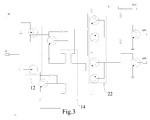
- FIG. 3 is a diagram schematically showing a drive circuit for a power supply according to the present invention.
- FIG. 4 is a diagram schematically showing another drive circuit for a power supply according to the present invention.
- FIG. 5 is a diagram schematically showing a half-bridge power source circuit according to the present invention.
- FIG. 6 is a diagram schematically showing a circuit wherein a half-bridge power source circuit and a drive circuit thereof are integrated according to the present invention.
- FIGS. 7-1 to FIGS. 7-4 are diagrams schematically showing all parts circuits of a circuit wherein the present invention is applied to a switched-mode power supply.
- FIG. 2 and FIGS. 7-1 to FIGS. 7-4 respectively a diagram schematically showing a circuit of a power supply according to the present invention and a diagram schematically showing all parts circuits of a circuit wherein the present invention is applied to a switched-mode power supply.
- an output rectifier/filter circuit 18 is connected to a half-bridge transformer 16 , arranged on the secondary side of the half-bridge transformer 16 and used to provide voltages for the external loads.
- a MOSFET (Metal Oxide Semiconductor Field Effect Transistor) unit 12 is connected to the other end of the half-bridge transformer 16 , arranged on the primary side of the half-bridge transformer 16 and used to drive the half-bridge transformer 16 .
- MOSFET Metal Oxide Semiconductor Field Effect Transistor
- the other end of the MOSFET unit 12 is connected to a separating element 14 , and the separating element 14 is used to separate the primary side and the secondary side.
- a totempole amplifier circuit 22 is connected to the other end of the separating element 14 .
- a PWM (Pulse Width Modulation) controller 20 is arranged on the secondary side, connected to the other end of the totempole amplifier circuit 22 and used to generate a control signal.
- the totempole amplifier circuit 22 amplifies the control signal.
- the amplified signal is received by the separating element 14 and used to drive the MOSFET unit 12 .
- the PWM controller 20 further comprises: a protection circuit 24 and an information-timing control circuit 26 .
- a voltage-feedback control circuit 28 is connected to the output rectifier/filter circuit 18 and the PWM controller 20 and used to modulate and balance the output voltage and the control signal.
- An independent power control circuit 30 provides an independent power source for the external loads so that the loads can keep on running when all the other portions of the system are shut off.
- An input rectifier/filter circuit 32 is connected to the half-bridge transformer 16 and converts the working voltage into a high-voltage DC current before the AC current enters the half-bridge transformer 16 .
- the MOSFET unit 12 performs energy conversion on the high-voltage DC current, and the converted energy is processed and then output by the output rectifier/filter circuit 18 .
- the PWM controller 20 provides a control signal, such as a small duty-cycle signal waveform.
- the totempole amplifier circuit 22 amplifies the small duty-cycle signal, and the separating element 14 receives the amplified signal and converts the voltage of the signal.
- the converted signal is used to drive the MOSFET unit 12 and further voltage-converted by the half-bridge transformer 16 .
- the output rectifier/filter circuit 18 processes the signal output by the half-bridge transformer 16 to provide voltages for the external loads.
- Such a circuit is usually used in a domestic power supply or a personal computer; therefore, the control signal is first transferred from the secondary side to the primary side, and then from the primary side back to the secondary side.
- the present invention is characterized in that the feedback controls of the output voltage are all on the secondary side.
- the totempole amplifier circuit 22 and the PWM controller 20 are integrated in a single chip.
- the totempole amplifier circuit 22 , the protection circuit 24 , the information-timing control circuit 26 and the PWM controller 20 may be integrated in a single chip. Thereby, the complexity and cost of circuit is reduced, and the production efficiency and product quality is promoted.
- the drive circuit of the present invention comprises: a totempole amplifier circuit 22 , a separating element 14 and a MOSFET unit 12 .
- the MOSFET unit 12 may be formed of two MOSFETs.
- the totempole amplifier circuit 22 can amplify the control signal before the separating element 14 receives the control signal. A low voltage should be converted into a high voltage before the separating element 14 can drive the MOSFET unit 12 .
- the totempole amplifier circuit 22 is used to make the separating element 14 able to provide sufficient instant current for the input capacitor Ciss, which is used to drive the MOSFET unit 12 .
- the MOSFETs can be driven much more easily.
- MOSFET does not have any transistor area and will not have too much switching loss during power conversion. Besides, as MOSFETs are voltage-operated components, it is easier for MOSFETs to increase the switching frequency of the power supply to over MHz. Further, as the half-bridge power source circuit can work in the first and third quadrants, the conversion efficiency can reach as high as 80% easily.
- the MOSFET unit 12 may be formed of a P-channel field effect transistor and an N-channel field effect transistor, or two P-channel field effect transistors, or two N-channel field effect transistors.
- FIG. 4 a diagram schematically showing another drive circuit for a power supply according to the present invention.
- a bipolar junction transistor unit 13 replaces the MOSFET unit 12 .
- the bipolar junction transistor unit 13 is formed of two bipolar junction transistors, such as a PNP transistor and a PNP transistor, or two NPN transistors, or two PNP transistors.
- FIG. 5 a diagram schematically showing a half-bridge power source circuit according to the present invention.
- FIG. 6 a diagram schematically showing a circuit wherein a half-bridge power source circuit and a drive circuit thereof are integrated according to the present invention.
- the MOSFET unit 12 is responsible for performing a driving activity in a positive or negative semi-period
- the operation of the power source circuit makes the half-bridge transformer 16 able to work in the first and third quadrants.
- the efficiency of the power supply can be promoted furthermore.
- the present invention integrates important circuits in an IC (such as the PWM controller, the protection circuit and the information-timing control circuit) and arranges the IC on the secondary side, which can prevent the important circuit from being damaged.
- the present invention adopts MOSFET, which can reduce power loss and increase the switching frequency of the power supply. Besides, the shortage of MOSFET is less likely to occur in the present environment, and the administration of fabrication and cost is thus easier.
Landscapes
- Engineering & Computer Science (AREA)
- Power Engineering (AREA)
- Dc-Dc Converters (AREA)
Abstract
Description
Claims (7)
Priority Applications (1)
| Application Number | Priority Date | Filing Date | Title |
|---|---|---|---|
| US11/964,662 US7729133B2 (en) | 2007-12-26 | 2007-12-26 | Secondary side-driven half-bridge power supply |
Applications Claiming Priority (1)
| Application Number | Priority Date | Filing Date | Title |
|---|---|---|---|
| US11/964,662 US7729133B2 (en) | 2007-12-26 | 2007-12-26 | Secondary side-driven half-bridge power supply |
Publications (2)
| Publication Number | Publication Date |
|---|---|
| US20090167081A1 US20090167081A1 (en) | 2009-07-02 |
| US7729133B2 true US7729133B2 (en) | 2010-06-01 |
Family
ID=40797282
Family Applications (1)
| Application Number | Title | Priority Date | Filing Date |
|---|---|---|---|
| US11/964,662 Expired - Fee Related US7729133B2 (en) | 2007-12-26 | 2007-12-26 | Secondary side-driven half-bridge power supply |
Country Status (1)
| Country | Link |
|---|---|
| US (1) | US7729133B2 (en) |
Families Citing this family (3)
| Publication number | Priority date | Publication date | Assignee | Title |
|---|---|---|---|---|
| US9966837B1 (en) | 2016-07-08 | 2018-05-08 | Vpt, Inc. | Power converter with circuits for providing gate driving |
| CN109596953B (en) * | 2018-12-20 | 2021-06-22 | 国网北京市电力公司 | Electromagnetic wave emission device and partial discharge test instrument |
| WO2021051254A1 (en) * | 2019-09-17 | 2021-03-25 | Redisem Ltd. | Controller for Power Converter |
Citations (3)
| Publication number | Priority date | Publication date | Assignee | Title |
|---|---|---|---|---|
| US5864472A (en) * | 1997-03-24 | 1999-01-26 | Ault Incorporated | Apparatus for controlling a multiresonant self-oscillating converter circuit |
| US6370040B2 (en) * | 2000-02-25 | 2002-04-09 | Murata Manufacturing Co., Ltd. | Switching power supply apparatus having plural outputs and plural output voltage detection |
| JP2003511004A (en) * | 1999-09-24 | 2003-03-18 | エリクソン インコーポレイテッド | External drive circuit for bridge type synchronous rectification |
-
2007
- 2007-12-26 US US11/964,662 patent/US7729133B2/en not_active Expired - Fee Related
Patent Citations (3)
| Publication number | Priority date | Publication date | Assignee | Title |
|---|---|---|---|---|
| US5864472A (en) * | 1997-03-24 | 1999-01-26 | Ault Incorporated | Apparatus for controlling a multiresonant self-oscillating converter circuit |
| JP2003511004A (en) * | 1999-09-24 | 2003-03-18 | エリクソン インコーポレイテッド | External drive circuit for bridge type synchronous rectification |
| US6370040B2 (en) * | 2000-02-25 | 2002-04-09 | Murata Manufacturing Co., Ltd. | Switching power supply apparatus having plural outputs and plural output voltage detection |
Also Published As
| Publication number | Publication date |
|---|---|
| US20090167081A1 (en) | 2009-07-02 |
Similar Documents
| Publication | Publication Date | Title |
|---|---|---|
| US9748834B2 (en) | Fast startup control circuit for switch mode power supply | |
| US6388514B1 (en) | Class D high voltage amplifier system with adaptive power supply | |
| US9595871B1 (en) | High efficiency inductive capacitive DC-DC converter | |
| US7402921B2 (en) | Method and apparatus for providing uninterruptible power | |
| US8724352B2 (en) | Power supply apparatus driving circuit, power supply apparatus driving integrated circuit, and power supply apparatus | |
| JP5938008B2 (en) | Power converter | |
| US20140139268A1 (en) | Driver circuit with tight control of gate voltage | |
| TWI596875B (en) | Buck converter with iii-nitride switch for substantially increased input-to-output voltage ratio | |
| JP2010528580A (en) | Multi-output synchronous flyback converter | |
| US11695321B2 (en) | Gate drive adapter | |
| JP5794855B2 (en) | Power supply drive circuit and power supply device | |
| JP6008330B2 (en) | Power converter | |
| CN113767557A (en) | Active clamp with bootstrap circuit | |
| US7729133B2 (en) | Secondary side-driven half-bridge power supply | |
| US9780690B2 (en) | Resonant decoupled auxiliary supply for a switched-mode power supply controller | |
| JP2005065497A (en) | Pulse-width modulation soft switching control | |
| CN104135144A (en) | Integrated primary startup bias and MOSFET driver | |
| JP5460138B2 (en) | Switching element drive circuit, converter | |
| US20110044075A1 (en) | Power converter capable of lowering power wastage on standby | |
| JP2011182482A (en) | Switching step-up type dc-dc converter and semiconductor integrated circuit device | |
| US8525499B2 (en) | Constant current switching power supply | |
| CN102468792B (en) | Drive unit of direct current brushless motor for fan | |
| US20240154577A1 (en) | Linear amplifier for providing sinusoidal waveform to load | |
| WO2007054886A2 (en) | Boost converter for power factor correction | |
| US20120319611A1 (en) | Boost Circuit for LED Backlight Driver Circuit |
Legal Events
| Date | Code | Title | Description |
|---|---|---|---|
| AS | Assignment |
Owner name: SOLYTECH ENTERPRISE CORPORATION, TAIWAN Free format text: ASSIGNMENT OF ASSIGNORS INTEREST;ASSIGNOR:CHEN, CHANG HSING;REEL/FRAME:020290/0818 Effective date: 20071213 Owner name: SOLYTECH ENTERPRISE CORPORATION,TAIWAN Free format text: ASSIGNMENT OF ASSIGNORS INTEREST;ASSIGNOR:CHEN, CHANG HSING;REEL/FRAME:020290/0818 Effective date: 20071213 |
|
| FPAY | Fee payment |
Year of fee payment: 4 |
|
| FEPP | Fee payment procedure |
Free format text: MAINTENANCE FEE REMINDER MAILED (ORIGINAL EVENT CODE: REM.) |
|
| LAPS | Lapse for failure to pay maintenance fees |
Free format text: PATENT EXPIRED FOR FAILURE TO PAY MAINTENANCE FEES (ORIGINAL EVENT CODE: EXP.) |
|
| STCH | Information on status: patent discontinuation |
Free format text: PATENT EXPIRED DUE TO NONPAYMENT OF MAINTENANCE FEES UNDER 37 CFR 1.362 |
|
| FP | Lapsed due to failure to pay maintenance fee |
Effective date: 20180601 |