EP4072009B1 - Symbol-leistungsverfolgungsversorgung und drahtlose vorrichtung mit einem durch die symbol-leistungsverfolgungsversorgung gespeisten verstärkersystem - Google Patents
Symbol-leistungsverfolgungsversorgung und drahtlose vorrichtung mit einem durch die symbol-leistungsverfolgungsversorgung gespeisten verstärkersystem Download PDFInfo
- Publication number
- EP4072009B1 EP4072009B1 EP21214935.5A EP21214935A EP4072009B1 EP 4072009 B1 EP4072009 B1 EP 4072009B1 EP 21214935 A EP21214935 A EP 21214935A EP 4072009 B1 EP4072009 B1 EP 4072009B1
- Authority
- EP
- European Patent Office
- Prior art keywords
- power
- voltage
- capacitor
- regulated
- charging
- Prior art date
- Legal status (The legal status is an assumption and is not a legal conclusion. Google has not performed a legal analysis and makes no representation as to the accuracy of the status listed.)
- Active
Links
Images





Classifications
-
- H—ELECTRICITY
- H03—ELECTRONIC CIRCUITRY
- H03F—AMPLIFIERS
- H03F1/00—Details of amplifiers with only discharge tubes, only semiconductor devices or only unspecified devices as amplifying elements
- H03F1/02—Modifications of amplifiers to raise the efficiency, e.g. gliding Class A stages, use of an auxiliary oscillation
- H03F1/0205—Modifications of amplifiers to raise the efficiency, e.g. gliding Class A stages, use of an auxiliary oscillation in transistor amplifiers
- H03F1/0211—Modifications of amplifiers to raise the efficiency, e.g. gliding Class A stages, use of an auxiliary oscillation in transistor amplifiers with control of the supply voltage or current
- H03F1/0216—Continuous control
- H03F1/0222—Continuous control by using a signal derived from the input signal
-
- H—ELECTRICITY
- H03—ELECTRONIC CIRCUITRY
- H03F—AMPLIFIERS
- H03F1/00—Details of amplifiers with only discharge tubes, only semiconductor devices or only unspecified devices as amplifying elements
- H03F1/02—Modifications of amplifiers to raise the efficiency, e.g. gliding Class A stages, use of an auxiliary oscillation
- H03F1/0205—Modifications of amplifiers to raise the efficiency, e.g. gliding Class A stages, use of an auxiliary oscillation in transistor amplifiers
- H03F1/0211—Modifications of amplifiers to raise the efficiency, e.g. gliding Class A stages, use of an auxiliary oscillation in transistor amplifiers with control of the supply voltage or current
- H03F1/0244—Stepped control
- H03F1/025—Stepped control by using a signal derived from the input signal
-
- H—ELECTRICITY
- H02—GENERATION; CONVERSION OR DISTRIBUTION OF ELECTRIC POWER
- H02M—APPARATUS FOR CONVERSION BETWEEN AC AND AC, BETWEEN AC AND DC, OR BETWEEN DC AND DC, AND FOR USE WITH MAINS OR SIMILAR POWER SUPPLY SYSTEMS; CONVERSION OF DC OR AC INPUT POWER INTO SURGE OUTPUT POWER; CONTROL OR REGULATION THEREOF
- H02M1/00—Details of apparatus for conversion
- H02M1/0067—Converter structures employing plural converter units, other than for parallel operation of the units on a single load
- H02M1/008—Plural converter units for generating at two or more independent and non-parallel outputs, e.g. systems with plural point of load switching regulators
-
- H—ELECTRICITY
- H02—GENERATION; CONVERSION OR DISTRIBUTION OF ELECTRIC POWER
- H02M—APPARATUS FOR CONVERSION BETWEEN AC AND AC, BETWEEN AC AND DC, OR BETWEEN DC AND DC, AND FOR USE WITH MAINS OR SIMILAR POWER SUPPLY SYSTEMS; CONVERSION OF DC OR AC INPUT POWER INTO SURGE OUTPUT POWER; CONTROL OR REGULATION THEREOF
- H02M3/00—Conversion of DC power input into DC power output
- H02M3/02—Conversion of DC power input into DC power output without intermediate conversion into AC
- H02M3/04—Conversion of DC power input into DC power output without intermediate conversion into AC by static converters
- H02M3/10—Conversion of DC power input into DC power output without intermediate conversion into AC by static converters using discharge tubes with control electrode or semiconductor devices with control electrode
- H02M3/145—Conversion of DC power input into DC power output without intermediate conversion into AC by static converters using discharge tubes with control electrode or semiconductor devices with control electrode using devices of a triode or transistor type requiring continuous application of a control signal
- H02M3/155—Conversion of DC power input into DC power output without intermediate conversion into AC by static converters using discharge tubes with control electrode or semiconductor devices with control electrode using devices of a triode or transistor type requiring continuous application of a control signal using semiconductor devices only
- H02M3/156—Conversion of DC power input into DC power output without intermediate conversion into AC by static converters using discharge tubes with control electrode or semiconductor devices with control electrode using devices of a triode or transistor type requiring continuous application of a control signal using semiconductor devices only with automatic control of output voltage or current, e.g. switching regulators
-
- H—ELECTRICITY
- H02—GENERATION; CONVERSION OR DISTRIBUTION OF ELECTRIC POWER
- H02M—APPARATUS FOR CONVERSION BETWEEN AC AND AC, BETWEEN AC AND DC, OR BETWEEN DC AND DC, AND FOR USE WITH MAINS OR SIMILAR POWER SUPPLY SYSTEMS; CONVERSION OF DC OR AC INPUT POWER INTO SURGE OUTPUT POWER; CONTROL OR REGULATION THEREOF
- H02M3/00—Conversion of DC power input into DC power output
- H02M3/02—Conversion of DC power input into DC power output without intermediate conversion into AC
- H02M3/04—Conversion of DC power input into DC power output without intermediate conversion into AC by static converters
- H02M3/10—Conversion of DC power input into DC power output without intermediate conversion into AC by static converters using discharge tubes with control electrode or semiconductor devices with control electrode
- H02M3/145—Conversion of DC power input into DC power output without intermediate conversion into AC by static converters using discharge tubes with control electrode or semiconductor devices with control electrode using devices of a triode or transistor type requiring continuous application of a control signal
- H02M3/155—Conversion of DC power input into DC power output without intermediate conversion into AC by static converters using discharge tubes with control electrode or semiconductor devices with control electrode using devices of a triode or transistor type requiring continuous application of a control signal using semiconductor devices only
- H02M3/156—Conversion of DC power input into DC power output without intermediate conversion into AC by static converters using discharge tubes with control electrode or semiconductor devices with control electrode using devices of a triode or transistor type requiring continuous application of a control signal using semiconductor devices only with automatic control of output voltage or current, e.g. switching regulators
- H02M3/158—Conversion of DC power input into DC power output without intermediate conversion into AC by static converters using discharge tubes with control electrode or semiconductor devices with control electrode using devices of a triode or transistor type requiring continuous application of a control signal using semiconductor devices only with automatic control of output voltage or current, e.g. switching regulators including plural semiconductor devices as final control devices for a single load
-
- H—ELECTRICITY
- H03—ELECTRONIC CIRCUITRY
- H03F—AMPLIFIERS
- H03F1/00—Details of amplifiers with only discharge tubes, only semiconductor devices or only unspecified devices as amplifying elements
- H03F1/02—Modifications of amplifiers to raise the efficiency, e.g. gliding Class A stages, use of an auxiliary oscillation
-
- H—ELECTRICITY
- H03—ELECTRONIC CIRCUITRY
- H03F—AMPLIFIERS
- H03F3/00—Amplifiers with only discharge tubes or only semiconductor devices as amplifying elements
- H03F3/189—High-frequency amplifiers, e.g. radio frequency amplifiers
- H03F3/19—High-frequency amplifiers, e.g. radio frequency amplifiers with semiconductor devices only
-
- H—ELECTRICITY
- H03—ELECTRONIC CIRCUITRY
- H03F—AMPLIFIERS
- H03F3/00—Amplifiers with only discharge tubes or only semiconductor devices as amplifying elements
- H03F3/189—High-frequency amplifiers, e.g. radio frequency amplifiers
- H03F3/19—High-frequency amplifiers, e.g. radio frequency amplifiers with semiconductor devices only
- H03F3/195—High-frequency amplifiers, e.g. radio frequency amplifiers with semiconductor devices only in integrated circuits
-
- H—ELECTRICITY
- H03—ELECTRONIC CIRCUITRY
- H03F—AMPLIFIERS
- H03F3/00—Amplifiers with only discharge tubes or only semiconductor devices as amplifying elements
- H03F3/20—Power amplifiers, e.g. Class B amplifiers, Class C amplifiers
- H03F3/21—Power amplifiers, e.g. Class B amplifiers, Class C amplifiers with semiconductor devices only
- H03F3/211—Power amplifiers, e.g. Class B amplifiers, Class C amplifiers with semiconductor devices only using a combination of several amplifiers
-
- H—ELECTRICITY
- H03—ELECTRONIC CIRCUITRY
- H03F—AMPLIFIERS
- H03F3/00—Amplifiers with only discharge tubes or only semiconductor devices as amplifying elements
- H03F3/20—Power amplifiers, e.g. Class B amplifiers, Class C amplifiers
- H03F3/21—Power amplifiers, e.g. Class B amplifiers, Class C amplifiers with semiconductor devices only
- H03F3/213—Power amplifiers, e.g. Class B amplifiers, Class C amplifiers with semiconductor devices only in integrated circuits
-
- H—ELECTRICITY
- H03—ELECTRONIC CIRCUITRY
- H03F—AMPLIFIERS
- H03F3/00—Amplifiers with only discharge tubes or only semiconductor devices as amplifying elements
- H03F3/20—Power amplifiers, e.g. Class B amplifiers, Class C amplifiers
- H03F3/24—Power amplifiers, e.g. Class B amplifiers, Class C amplifiers of transmitter output stages
- H03F3/245—Power amplifiers, e.g. Class B amplifiers, Class C amplifiers of transmitter output stages with semiconductor devices only
-
- H—ELECTRICITY
- H03—ELECTRONIC CIRCUITRY
- H03G—CONTROL OF AMPLIFICATION
- H03G3/00—Gain control in amplifiers or frequency changers
- H03G3/20—Automatic control
- H03G3/30—Automatic control in amplifiers having semiconductor devices
- H03G3/3036—Automatic control in amplifiers having semiconductor devices in high-frequency amplifiers or in frequency-changers
- H03G3/3042—Automatic control in amplifiers having semiconductor devices in high-frequency amplifiers or in frequency-changers in modulators, frequency-changers, transmitters or power amplifiers
-
- H—ELECTRICITY
- H04—ELECTRIC COMMUNICATION TECHNIQUE
- H04B—TRANSMISSION
- H04B1/00—Details of transmission systems, not covered by a single one of groups H04B3/00 - H04B13/00; Details of transmission systems not characterised by the medium used for transmission
- H04B1/02—Transmitters
- H04B1/04—Circuits
-
- H—ELECTRICITY
- H04—ELECTRIC COMMUNICATION TECHNIQUE
- H04B—TRANSMISSION
- H04B7/00—Radio transmission systems, i.e. using radiation field
- H04B7/02—Diversity systems; Multi-antenna system, i.e. transmission or reception using multiple antennas
- H04B7/04—Diversity systems; Multi-antenna system, i.e. transmission or reception using multiple antennas using two or more spaced independent antennas
- H04B7/0413—MIMO systems
- H04B7/0452—Multi-user MIMO systems
-
- H—ELECTRICITY
- H03—ELECTRONIC CIRCUITRY
- H03F—AMPLIFIERS
- H03F2200/00—Indexing scheme relating to amplifiers
- H03F2200/102—A non-specified detector of a signal envelope being used in an amplifying circuit
-
- H—ELECTRICITY
- H03—ELECTRONIC CIRCUITRY
- H03F—AMPLIFIERS
- H03F2200/00—Indexing scheme relating to amplifiers
- H03F2200/451—Indexing scheme relating to amplifiers the amplifier being a radio frequency amplifier
-
- H—ELECTRICITY
- H03—ELECTRONIC CIRCUITRY
- H03F—AMPLIFIERS
- H03F2200/00—Indexing scheme relating to amplifiers
- H03F2200/504—Indexing scheme relating to amplifiers the supply voltage or current being continuously controlled by a controlling signal, e.g. the controlling signal of a transistor implemented as variable resistor in a supply path for, an IC-block showed amplifier
-
- H—ELECTRICITY
- H03—ELECTRONIC CIRCUITRY
- H03F—AMPLIFIERS
- H03F2200/00—Indexing scheme relating to amplifiers
- H03F2200/507—A switch being used for switching on or off a supply or supplying circuit in an IC-block amplifier circuit
-
- H—ELECTRICITY
- H03—ELECTRONIC CIRCUITRY
- H03F—AMPLIFIERS
- H03F2200/00—Indexing scheme relating to amplifiers
- H03F2200/511—Many discrete supply voltages or currents or voltage levels can be chosen by a control signal in an IC-block amplifier circuit
-
- H—ELECTRICITY
- H04—ELECTRIC COMMUNICATION TECHNIQUE
- H04B—TRANSMISSION
- H04B1/00—Details of transmission systems, not covered by a single one of groups H04B3/00 - H04B13/00; Details of transmission systems not characterised by the medium used for transmission
- H04B1/02—Transmitters
- H04B1/04—Circuits
- H04B2001/0408—Circuits with power amplifiers
Definitions
- the present invention relates to a symbol power tracking (SPT) amplification design in a wireless device.
- SPT symbol power tracking
- a wireless device usually requires a radio-frequency power amplifier (RF PA) that converts low-power radio signals to higher power signals to drive an antenna of a transmitter.
- RF PA radio-frequency power amplifier
- the supply voltage VPA of the RF PA typically is modulated for symbol power tracking (SPT).
- FIG. 1A depicts a conventional SPT amplification design in a wireless device 100.
- a power amplifier 102 and a dc-dc converter 104 form an SPT amplification system to drive an antenna 106 of a transmitter of the wireless device 100.
- the dc-dc converter 104 uses a dc-dc switch mode power supply (SMPS) buck 108, an inductor L, and a capacitor C to generate an adaptive supply voltage VPA (i.e., an SPT supply voltage) that tracks the power of the radio frequency (RF) signals to be transmitted by the antenna 106.
- FIG. 1B shows the SPT supply voltage VPA and the RF signals. As shown, power consumption can be greatly reduced by the SPT supply voltage VPA.
- SMPS dc-dc switch mode power supply
- RF radio frequency
- the conventional SPT amplification design may result in some problems in high-speed applications (e.g., 5G communication applications).
- the capacitor C used to regulate the SPT supply voltage VPA typically is huge, e.g., up to several ⁇ F. It takes a long time to charge or discharge such a large capacitor C for SPT.
- the cyclic prefix section (CP, prior to each symbol section) for VPA transition is short, e.g., 0.29 ⁇ s.
- Patent documents EP3565115A1 SAMSUNG ELECTRONICS CO LTD [KR]) 6 November 2019 (2019-11-06) and WO2020/206246A1 (APPLE INC [US]) 8 October 2020 (2020-10-08) disclose relevant symbol power tracking supply modulators of the prior art.
- a fast tracking and low loss symbol-power-tracking (SPT) supply that powers a radio-frequency power amplifier (RF PA) (or any electronic element) is shown.
- An SPT supply in accordance with an exemplary embodiment of the present invention has a power converter, a transition capacitor, an assisted charging and discharging circuit, and a multi-level array.
- the power converter is coupled to an output port of an input power source for power conversion, and has an output terminal coupled to a power terminal of the RFPA.
- the transition capacitor is coupled to the power terminal of the radio-frequency power amplifier though the output terminal of the power converter.
- the assisted charging and discharging circuit may be coupled to the transition capacitor during cyclic prefix (CP) sections.
- the multi-level array includes a plurality of voltage-regulated capacitors which are pre-charged to and kept at different voltage levels.
- a target capacitor at a fixed voltage level matching the current SPT situation may be selected from among the voltage-regulated capacitors to be coupled to the power terminal of the radio-frequency power amplifier.
- Each voltage-regulated capacitor is kept at a fixed voltage level.
- the different voltage levels provided by the different voltage-regulated capacitors match the different SPT supply levels. Rather than periodically charge/discharge a large capacitor, the supply voltage for the RF PA is easily changed to meet the dynamically changed SPT situation by switching the connections between the voltage-regulated capacitors and the power terminal of the radio-frequency power amplifier.
- the voltage-regulated capacitors are pre-charged to the different voltage levels during a power-on period.
- the different voltage-regulated capacitors relate to the different thresholds. When a voltage-regulated capacitor whose voltage level decreases to lower than its corresponding threshold is disconnected from the power terminal of the radio-frequency power amplifier, the voltage-regulated capacitor can be charged to compensate for current leakage.
- the voltage-regulated capacitors are pre-charged to the different voltage levels during a power-on period.
- the different voltage-regulated capacitors corresponding to different thresholds; and when a voltage-regulated capacitor whose voltage level decreases to lower than its corresponding threshold is disconnected from the power terminal of the electronic element, the voltage-regulated capacitor is charged to compensate for current leakage.
- each voltage-regulated capacitor is more than an order of magnitude larger in size than the transition capacitor.
- the assisted charging and discharging circuit is coupled to the transition capacitor during cyclic prefix sections; and during each symbol section, the target capacitor and the transition capacitor are connected in parallel.
- the multi-level array further comprises voltage regulation switches that correspond one-to-one with the voltage-regulated capacitors, and each voltage regulation switch is coupled between the corresponding voltage-regulated capacitor and the power terminal of the electronic element; all voltage regulation switches are open during cyclic prefix sections; the assisted charging and discharging circuit is coupled to the transition capacitor during the cyclic prefix sections; and when a voltage-regulated capacitor is selected as the target capacitor during each symbol section, the corresponding voltage regulation switch is closed to couple the target capacitor to the power terminal of the electronic element.
- FIG. 2 illustrates a wireless device 200 in accordance with an exemplary embodiment of the preset invention.
- Radio frequency (RF) signals are amplified by an array of power amplifiers (PAs) to be transmitted by an antenna 202.
- a supply is shown in FIG. 2 , which transforms the power of an input power source 204 (e.g., a battery) to a symbol-power-tracking (SPT) supply voltage VPA to power an RF PA PA Array .
- an input power source 204 e.g., a battery
- SPT symbol-power-tracking
- the SPT supply has a power converter 206, a transition capacitor Ctran, an assisted charging and discharging circuit 208, and a multi-level array 210.
- An output port of the input power source 204 is coupled to the power converter 206 for power conversion.
- the power converter 206 has an output terminal coupled to a power terminal of the RF PA PA Array .
- the transition capacitor Ctran (coupled to the power terminal of the RF PA PA Array through the output terminal of the power converter 206) and the multi-level array 210 including a plurality of voltage-regulated capacitors are provided for voltage regulation.
- An SPT supply voltage VPA is applied to the power terminal of the PA array.
- each voltage-regulated capacitor in the multi-level array 210 is more than an order of magnitude larger in size.
- the voltage-regulated capacitors in the multi-level array 210 are pre-charged to and kept at different voltage levels. Note that each voltage-regulated capacitor is kept at a fixed voltage level. During each symbol section, the voltage-regulated capacitor regulated at a fixed voltage level matching the current SPT situation is selected as a target capacitor to be coupled to the power terminal of the RF PA PA Array .
- the SPT supply voltage VPA is easily changed to meet the current SPT situation by switching the connections between the voltage-regulated capacitors (provided in the multi-level array 210) and the power terminal of the RF PA PA Array .
- FIG. 3A depicts the details of a power converter 302, an assisted charging and discharging circuit 304, and a multi-level array 306 in accordance with an exemplary embodiment of the present invention.
- the power converter 302 is a dc-dc converter (a buck circuit).
- the buck circuit 302 may be replaced by a boost circuit or a buck-boost circuit.
- the multi-level array 306 includes voltage-regulated capacitors C1, C2, C3 and C4, a pre-charging design (controlled by signals VPC1 ⁇ VPC4 and VPD1 ⁇ VPD4) for the voltage-regulated capacitors C1 ⁇ C4, and voltage regulation switches sw1 ⁇ sw4 (corresponding to the voltage-regulated capacitors C1 ⁇ C4 one to one).
- Each voltage regulation switch is coupled between its corresponding voltage-regulated capacitor and the power terminal of the RF PA PA Array (to control the SPT supply voltage VPA).
- the power converter 302 may be turned off (by controlling the signals VDA and VDB), and the assisted charging and discharging circuit 304 may be turned off, too.
- the voltage regulation switches sw1 ⁇ sw4 are open (by controlling the signals VP1 to VP4), and the voltage-regulated capacitors C1 ⁇ C4 are pre-charged to their expected fixed voltage levels by the pre-charging design (controlled by signals VPC1 ⁇ VPC4 and VPD1 ⁇ VPD4).
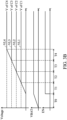
- FIG. 3B depicts the waveforms of the voltage levels of the voltage-regulated capacitors C1 ⁇ C4, the battery power VBAT, and the enable signal EN indicating the ready status of the battery power VBAT.
- the waveforms changes step by step as shown in the timing intervals T0 ⁇ T4.
- the battery power VBAT is gradually turned on in timing interval T0 and, when the battery power is ready, the enable signal EN is asserted.
- the asserted enable signal EN the pre-charging of the voltage-regulated capacitors C1 ⁇ C4 starts, and all of the control signals VPC1 ⁇ VPC4 are low to establish charging paths for the voltage-regulated capacitors C1 ⁇ C4.
- the voltage-regulated capacitor C1 reaches the first fixed voltage level VL1, and the control signal VPC1 changes high to break the charging path of the voltage-regulated capacitor C1.
- the voltage-regulated capacitor C2 reaches the second fixed voltage level VL2, and the control signal VPC2 changes high to break the charging path of the voltage-regulated capacitor C2.
- the voltage-regulated capacitor C3 reaches the third fixed voltage level VL3, and the control signal VPC3 changes high to break the charging path of the voltage-regulated capacitor C3.
- the voltage-regulated capacitor C4 reaches the fourth fixed voltage level VL4, and the control signal VPC4 changes high to break the charging path of the voltage-regulated capacitor C4.
- the connection of the regulation capacitors (including the transition capacitor Ctran and the voltage-regulated capacitors C1 ⁇ C4) are discussed in the following paragraphs.
- FIG. 3C shows two consecutive symbol sections Symbol1 and Symbol2.
- a first cyclic prefix (CP) section CP1 is required prior to the first symbol section Symbol1
- a second cyclic prefix (CP) section CP2 is required prior to the second symbol section Symbol2.
- the SPT supply voltage VPA should be VL1.
- the SPT supply voltage VPA should be VL4.
- the supply voltage VPA should transit from the previous level to the expected voltage level VL1.
- the supply voltage VPA should transit from VL1 to VL4.
- the transition capacitor Ctran is discharged by the assisted charging and discharging circuit 304 to the expected voltage level VL1.
- the voltage regulation switch sw1 is closed, so that the voltage-regulated capacitor C1 (kept at the voltage level VL1) and the transition capacitor Ctran are connected in parallel between the power terminal of the RF PA PA Array and the ground to provide a stable SPT supply voltage VL1 as VPA. Because the transition capacitor Ctran is much smaller than the voltage-regulated capacitor C1, it is OK to discharge the transition capacitor Ctran to the expected voltage level VL1 in the short CP section (e.g., 0.29 ⁇ s for 5G applications).
- the large voltage-regulated capacitor C1 can provide strong regulation capability in the first symbol section Symbol1.
- all voltage regulation switches sw1 ⁇ sw4 are open, and the transition capacitor Ctran is charged by the assisted charging and discharging circuit 304 from VL1 to VL4.
- the voltage regulation switch sw4 is closed, so that the voltage-regulated capacitor C4 (kept at the voltage level VL4) and the transition capacitor Ctran are connected in parallel between the power terminal of the RF PA PA Array and the ground to provide a stable SPT supply voltage VL4 as VPA.
- the small-sized transition capacitor Ctran is rapidly charged to the expected voltage level VL4 in the short CP section CP2.
- the large voltage-regulated capacitor C4 can provide strong regulation capability in the second symbol section Symbol2.
- a current leakage solution for the voltage-regulated capacitors C1 ⁇ C4 are introduced in the present invention.
- the different voltage-regulated capacitors relate to the different thresholds.
- the voltage-regulated capacitor can be charged to compensate for current leakage.
- the control signals VPC2 ⁇ VPC4 can be switched to low to establish charging paths for the other voltage-regulated capacitors C2 ⁇ C4, and thereby the voltage-regulated capacitors C2 ⁇ C4 are charged back to their fixed voltage levels VL2 ⁇ VL4.
- the control signals VPC1 ⁇ VPC3 can be switched to low to establish charging paths for the other voltage-regulated capacitors C1 ⁇ C3, and thereby the voltage-regulated capacitors C1 ⁇ C3 are charged back to their fixed voltage levels VL1 ⁇ VL3.
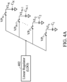
- FIGs 4A ⁇ 4D show several embodiments of the multi-level array 210.
- the multi-level array comprises a plurality of charging switches (controlled by signals VP1 ⁇ VPN) that correspond one-to-one with the voltage-regulated capacitors C1 ⁇ CN.
- Each charging switch is closed to establish a pre-charging path for one voltage-regulated capacitor until the voltage-regulated capacitor is pre-charged to its expected fixed voltage level.
- the corresponding charging switch is closed again until the voltage-regulated capacitor is charged back to its expected fixed fixed voltage level.
- the multi-level array comprises one single linear regulator 402, which is coupled to the voltage-regulated capacitors C1 ⁇ CN through the charging switches for capacitor charging.
- the multi-level array comprises a plurality of linear regulators LDO1 ⁇ LDON that correspond one-to-one with the voltage-regulated capacitors C1 ⁇ CN.
- Each linear regulator is coupled to one voltage-regulated capacitor through one charging switch to charge the corresponding voltage-regulated capacitor.
- pre-charging of the voltage-regulated capacitors C1 ⁇ CN is planned in the power-on period, there is sufficient time for the slow LDO to pre-charge the voltage-regulated capacitors C1 ⁇ CN to the fixed voltage levels VL1 ⁇ VLN.
- the circuit cost can be reduced. However, it is not limited to using LDO technique for pre-charging the voltage-regulated capacitors C1 ⁇ CN.
- the multi-level array comprises a single-input and multiple-output (SIMO) dc-dc converter (a buck, a boost, or a buck-boost circuit) 404, to be coupled to the voltage-regulated capacitors C1 ⁇ CN through the charging switches for capacitor charging.
- SIMO single-input and multiple-output
- the multi-level array comprises a plurality of switched-mode power supplies (SMPS, e.g., a buck, a boost, or a buck-boost circuit) SMPS1 ⁇ SMPSN corresponding to the voltage-regulated capacitors C1 ⁇ CN one to one.
- SMPS switched-mode power supply
- Each switched-mode power supply (SMPS) is coupled to its corresponding voltage-regulated capacitor, through the corresponding charging switch, for capacitor charging.
- FIGs 5A ⁇ 5D show several embodiments of the assisted charging and discharging circuit 208.
- the assisted charging and discharging circuit comprises two sets of current sources 502 and 504.
- the first set of current sources 502 includes current sources which are turned on in several manners (by switching the control signals VC1 ⁇ VCN) to provide different charging currents for the transition capacitor Ctran.
- the second set of current sources 504 includes current sources which are turned on in several manners (by switching the control signals VD1 ⁇ VDN) to provide different discharging currents for the transition capacitor Ctran.
- the assisted charging and discharging circuit comprises a linear regulator 506 and one set of current sources 508.
- the linear regulator 506 is operated (according to a feedback voltage VFB and a reference voltage VREF) to charge the transition capacitor Ctran.
- the set of current sources 508 includes current sources which are turned on in several manners (by switching the control signals VD1 ⁇ VDN) to provide different discharging currents for the transition capacitor Ctran.
- the assisted charging and discharging circuit comprises one set of current sources 510 and a linear regulator 512.
- the set of current sources 510 includes current sources which are turned on in several manners (by switching the control signals VC1 ⁇ VCN) to provide different charging currents for the transition capacitor Ctran.
- the linear regulator 512 is operated to discharge the transition capacitor Ctran.
- the assisted charging and discharging circuit comprises two linear regulators 514 and 516.
- the linear regulator 514 is operated to charge the transition capacitor Ctran.
- the linear regulator 516 is operated to discharge the transition capacitor Ctran.
- Any amplification system for a wireless device uses the multi-level array 210 should be considered within the scope of the present invention.
- the forgoing SPT supply may be applied to power other electronic elements rather than a power amplifier.
- the timing to charge/discharge the transition capacitor Ctran is not limited to cyclic prefix sections, and the timing to connect a target capacitor (selected from the voltage-regulated capacitors within the multi-level array) and the transition capacitor Ctran in parallel is not limited to the symbol sections. There may be some timing shift considering the circuit delays.
Landscapes
- Engineering & Computer Science (AREA)
- Power Engineering (AREA)
- Computer Networks & Wireless Communication (AREA)
- Signal Processing (AREA)
- Microelectronics & Electronic Packaging (AREA)
- Direct Current Feeding And Distribution (AREA)
- Dc-Dc Converters (AREA)
- Amplifiers (AREA)
- Transmitters (AREA)
Claims (14)
- Symbol-Leistungsverfolgungsversorgung, umfassend:einen Leistungswandler (206), der zur Leistungswandlung mit einem Ausgabeport einer Eingabeleistungsquelle (204) gekoppelt ist, und ein mit einem Leistungsterminal eines elektronischen Elements gekoppeltes Ausgabeterminal aufweist;einen Übergangskondensator (Ctran), der über das Ausgabeterminal des Leistungswandlers mit dem Leistungsterminal des elektronischen Elements gekoppelt ist;eine unterstützte Lade- und Entladeschaltung (208), die mit dem Übergangskondensator gekoppelt ist; undein Multi-Pegel-Array (210, 306), das eine Vielzahl von spannungsgeregelten Kondensatoren (C1-C4) einschließt, die während einer Einschaltperiode auf verschiedene fixierte Spannungspegel vorgeladen und auf den fixierten Spannungspegeln gehalten werden, wobei ein Zielkondensator aus der Vielzahl von spannungsgeregelten Kondensatoren ausgewählt wird, um mit dem Leistungsterminal gekoppelt zu werden;wobei:die unterstützte Lade- und Entladeschaltung den Übergangskondensator während einer zyklischen Präfix-Sektion auf einen Symbol-Leistungsverfolgungspegel lädt oder entlädt; undwährend einer auf die zyklische Präfix-Sektion folgenden Symbol-Sektion ein spannungsgeregelter Kondensator, der auf einem fixierten Spannungspegel gehalten wird, der derselbe wie der Symbol-Leistungsverfolgungspegel ist, als der Zielkondensator ausgewählt wird, der mit dem Leistungsterminal des elektronischen Elements gekoppelt werden soll.
- Symbol-Leistungsverfolgungsversorgung nach Anspruch 1, wobei:das Multi-Pegel-Array weiter Ladeschalter umfasst, die eins zu eins den spannungsgeregelten Kondensatoren entsprechen;jeder Ladeschalter geschlossen wird, um einen Vorlade-Pfad des entsprechenden spannungsgeregelten Kondensators herzustellen, bis der entsprechende spannungsgeregelte Kondensator auf seinen erwarteten fixierten Spannungspegel vorgeladen ist.
- Symbol-Leistungsverfolgungsversorgung nach Anspruch 2, wobei:die verschiedenen spannungsgeregelten Kondensatoren verschiedenen Schwellenwerten entsprechen; undwenn ein spannungsgeregelter Kondensator, dessen Spannungspegel unter seinen entsprechenden Schwellenwert abnimmt, von dem Leistungsterminal des elektronischen Elements getrennt wird, der entsprechende Ladeschalter wieder geschlossen wird, bis der spannungsgeregelte Kondensator wieder auf seinen erwarteten fixierten Spannungspegel geladen ist.
- Symbol-Leistungsverfolgungsversorgung nach Anspruch 3, wobei:
das Multi-Pegel-Array weiter einen einzigen linearen Regler umfasst, der über die Ladeschalter zum Kondensatorladen mit den spannungsgeregelten Kondensatoren gekoppelt werden soll. - Symbol-Leistungsverfolgungsversorgung nach Anspruch 3, wobei:das Multi-Pegel-Array weiter lineare Regler umfasst, die eins zu eins den spannungsgeregelten Kondensatoren entsprechen; undjeder lineare Regler über den entsprechenden Ladeschalter mit dem entsprechenden spannungsgeregelten Kondensator gekoppelt ist, zum Kondensatorladen.
- Symbol-Leistungsverfolgungsversorgung nach Anspruch 3, wobei:
das Multi-Pegel-Array weiter einen Einzel-Eingabe- und Mehrfach-Ausgabe-DC-DC-Wandler umfasst, der über die Ladeschalter zum Kondensatorladen mit den spannungsgeregelten Kondensatoren gekoppelt werden soll. - Symbol-Leistungsverfolgungsversorgung nach Anspruch 3, wobei:
das Multi-Pegel-Array weiter Umschaltmodus-Leistungsversorgungen umfasst, die eins zu eins den spannungsgeregelten Kondensatoren entsprechen; und jede Umschaltmodus-Leistungsversorgung über den entsprechenden Ladeschalter mit dem entsprechenden spannungsgeregelten Kondensator gekoppelt ist, zum Kondensatorladen. - Symbol-Leistungsverfolgungsversorgung nach einem der vorstehenden Ansprüche, wobei die unterstützte Lade- und Entladeschaltung folgendes umfasst:einen ersten Satz von Stromquellen, die Stromquellen einschließen, die auf verschiedene Arten eingeschaltet werden, um unterschiedliche Ladeströme für den Übergangskondensator bereitzustellen; undeinen zweiten Satz von Stromquellen, die Stromquellen einschließen, die auf verschiedene Arten eingeschaltet werden, um unterschiedliche Entladeströme für den Übergangskondensator bereitzustellen.
- Symbol-Leistungsverfolgungsversorgung nach einem der Ansprüche 1 bis 7, wobei die unterstützte Lade- und Entladeschaltung folgendes umfasst:einen linearen Regler zum Laden des Übergangskondensators; undeinen Satz von Stromquellen, die Stromquellen einschließen, die auf verschiedene Arten eingeschaltet werden, um unterschiedliche Entladeströme für den Übergangskondensator bereitzustellen.
- Symbol-Leistungsverfolgungsversorgung nach einem der Ansprüche 1 bis 7, wobei die unterstützte Lade- und Entladeschaltung folgendes umfasst:einen Satz von Stromquellen, die Stromquellen einschließen, die auf verschiedene Arten eingeschaltet werden, um unterschiedliche Ladeströme für den Übergangskondensator bereitzustellen; undeinen linearen Regler zum Entladen des Übergangskondensators.
- Symbol-Leistungsverfolgungsversorgung nach einem der Ansprüche 1 bis 7, wobei die unterstützte Lade- und Entladeschaltung folgendes umfasst:einen ersten linearen Regler zum Laden des Übergangskondensators; undeinen zweiten linearen Regler zum Entladen des Übergangskondensators.
- Symbol-Leistungsverfolgungsversorgung nach einem der vorstehenden Ansprüche, wobei:
der Leistungswandler ein DC-DC-Wandler ist. - Symbol-Leistungsverfolgungsversorgung nach einem der vorstehenden Ansprüche, wobei:
das Multi-Pegel-Array weiter Spannungsregelungsschalter umfasst, die eins zu eins den spannungsgeregelten Kondensatoren entsprechen, und jeder Spannungsregelungsschalter zwischen dem entsprechenden spannungsgeregelten Kondensator und dem Leistungsterminal des elektronischen Elements gekoppelt ist. - Drahtlose Vorrichtung, umfassend:Symbol-Leistungsverfolgungsversorgung, wie in einem der Ansprüche 1 bis 13 beansprucht;einen Hochfrequenz-Leistungsverstärker, der das elektronische Element ist, das von der Symbol-Leistungsverfolgungsversorgung mit Leistung versorgt wird; undeine Antenne, die Funksignale überträgt, die von dem Hochfrequenz-Leistungsverstärker bereitgestellt werden.
Applications Claiming Priority (2)
| Application Number | Priority Date | Filing Date | Title |
|---|---|---|---|
| US202163171123P | 2021-04-06 | 2021-04-06 | |
| US17/515,925 US20220321060A1 (en) | 2021-04-06 | 2021-11-01 | Symbol-power-tracking supply, and wireless device using amplification system powered by the symbol-power-tracking supply |
Publications (3)
| Publication Number | Publication Date |
|---|---|
| EP4072009A2 EP4072009A2 (de) | 2022-10-12 |
| EP4072009A3 EP4072009A3 (de) | 2022-10-19 |
| EP4072009B1 true EP4072009B1 (de) | 2025-05-14 |
Family
ID=79024387
Family Applications (1)
| Application Number | Title | Priority Date | Filing Date |
|---|---|---|---|
| EP21214935.5A Active EP4072009B1 (de) | 2021-04-06 | 2021-12-15 | Symbol-leistungsverfolgungsversorgung und drahtlose vorrichtung mit einem durch die symbol-leistungsverfolgungsversorgung gespeisten verstärkersystem |
Country Status (4)
| Country | Link |
|---|---|
| US (1) | US20220321060A1 (de) |
| EP (1) | EP4072009B1 (de) |
| CN (1) | CN115208192A (de) |
| TW (1) | TWI826892B (de) |
Families Citing this family (3)
| Publication number | Priority date | Publication date | Assignee | Title |
|---|---|---|---|---|
| KR102872190B1 (ko) * | 2021-07-05 | 2025-10-15 | 삼성전자주식회사 | 전력 노이즈 필터 및 이를 포함하는 전원 변조기 |
| US12007821B2 (en) * | 2022-04-08 | 2024-06-11 | Monolithic Power Systems, Inc. | Power loss prevention circuit with mitigation for failed energy storage banks |
| CN121710676A (zh) * | 2024-09-20 | 2026-03-20 | 华为技术有限公司 | 符号功率跟踪电源、符号功率跟踪放大系统及符号调压方法 |
Citations (3)
| Publication number | Priority date | Publication date | Assignee | Title |
|---|---|---|---|---|
| US20100007536A1 (en) * | 2007-06-08 | 2010-01-14 | Michiko Tokumaru | Rapid recovery circuit |
| US20190334480A1 (en) * | 2018-04-30 | 2019-10-31 | Samsung Electronics Co., Ltd. | Symbol power tracking amplification system and a wireless communication device including the same |
| US20190386565A1 (en) * | 2018-03-28 | 2019-12-19 | Qualcomm Incorporated | Methods and apparatuses for voltage regulation using predictively charged precharge rails |
Family Cites Families (7)
| Publication number | Priority date | Publication date | Assignee | Title |
|---|---|---|---|---|
| CN101371603B (zh) * | 2006-01-11 | 2013-10-23 | 高通股份有限公司 | 无线对等网络中的无线设备发现 |
| CN103513684A (zh) * | 2012-06-18 | 2014-01-15 | 哈尔滨智木科技有限公司 | 一种大电流恒流源实现方法 |
| US9948312B2 (en) * | 2016-02-29 | 2018-04-17 | Texas Instruments Incorporated | Phase lock loop with a digital charge pump |
| JP7393876B2 (ja) * | 2018-04-30 | 2023-12-07 | 三星電子株式会社 | シンボル電力追跡増幅システム及びそれを含む無線通信装置 |
| EP3565115A1 (de) * | 2018-04-30 | 2019-11-06 | Samsung Electronics Co., Ltd. | Symbolleistungsverfolgungsverstärkungssystem und drahtloskommunikationsvorrichtung damit |
| WO2020206246A1 (en) * | 2019-04-03 | 2020-10-08 | Apple Inc. | DIGITAL ENVELOPE TRACKER FOR mmWAVE SYMBOL POWER TRACKING AND DIGITAL ENVELOPE TRACKER FOR MULTIPLE-TX CHANNELS WITH SHARED-RESOURCE VOLTAGE REGULATOR |
| US11223325B2 (en) * | 2019-09-27 | 2022-01-11 | Skyworks Solutions, Inc. | Multi-level envelope tracking systems with adjusted voltage steps |
-
2021
- 2021-11-01 US US17/515,925 patent/US20220321060A1/en not_active Abandoned
- 2021-12-15 EP EP21214935.5A patent/EP4072009B1/de active Active
-
2022
- 2022-01-03 TW TW111100022A patent/TWI826892B/zh active
- 2022-01-27 CN CN202210103066.8A patent/CN115208192A/zh not_active Withdrawn
Patent Citations (3)
| Publication number | Priority date | Publication date | Assignee | Title |
|---|---|---|---|---|
| US20100007536A1 (en) * | 2007-06-08 | 2010-01-14 | Michiko Tokumaru | Rapid recovery circuit |
| US20190386565A1 (en) * | 2018-03-28 | 2019-12-19 | Qualcomm Incorporated | Methods and apparatuses for voltage regulation using predictively charged precharge rails |
| US20190334480A1 (en) * | 2018-04-30 | 2019-10-31 | Samsung Electronics Co., Ltd. | Symbol power tracking amplification system and a wireless communication device including the same |
Non-Patent Citations (1)
| Title |
|---|
| PAEK JI-SEON ET AL: "15.2 A 90ns/V Fast-Transition Symbol-Power-Tracking Buck Converter for 5G mm-Wave Phased-Array Transceiver", 2019 IEEE INTERNATIONAL SOLID- STATE CIRCUITS CONFERENCE - (ISSCC), IEEE, 17 February 2019 (2019-02-17), pages 240 - 242, XP033527913, DOI: 10.1109/ISSCC.2019.8662420 * |
Also Published As
| Publication number | Publication date |
|---|---|
| TW202241030A (zh) | 2022-10-16 |
| US20220321060A1 (en) | 2022-10-06 |
| TWI826892B (zh) | 2023-12-21 |
| EP4072009A3 (de) | 2022-10-19 |
| EP4072009A2 (de) | 2022-10-12 |
| CN115208192A (zh) | 2022-10-18 |
Similar Documents
| Publication | Publication Date | Title |
|---|---|---|
| US9595869B2 (en) | Multi-level switching regulator circuits and methods with finite state machine control | |
| EP4072009A2 (de) | Symbol-leistungsverfolgungsversorgung und drahtlose vorrichtung mit einem durch die symbol-leistungsverfolgungsversorgung gespeisten verstärkersystem | |
| US9628118B2 (en) | Adaptive envelope tracking for biasing radio frequency power amplifiers | |
| EP1922802B1 (de) | Spitzenladestrommodulation für burst-modus-wandlung | |
| CN109905813B (zh) | 自适应伪闭环电荷泵电路 | |
| US12323055B2 (en) | Driver circuitry and operation | |
| US10879796B2 (en) | DC-DC converter with fast voltage charging circuitry for Wi-Fi cellular applications | |
| US20210034085A1 (en) | Charge Pump Transient Response Optimization by Controlled Flying Capacitor Discharge During Bypass to Switching Mode Transition | |
| GB2460072A (en) | Multiple voltage level supply stage | |
| EP1982400A1 (de) | Stromversorgung für begrenzte stromquellen und audioverstärker mit einer stromversorgung | |
| WO2008034126A2 (en) | Frequency regulated hysteretic average current mode converter | |
| EP1264382A2 (de) | Extrem- niedrige- leistungsschaltregelungsverfahren und vorrichtung mit adaptiver regelung der schaltfrequenz und des spitzenstromauslösepunkts | |
| US10972003B2 (en) | Charge pump | |
| US7851941B2 (en) | Method and system for a multiple output capacitive buck/boost converter | |
| KR20110040700A (ko) | 샘플 및 홀드 피드백 제어를 갖는 회로 및 방법 | |
| US7173403B1 (en) | Boost DC/DC converter | |
| KR102204422B1 (ko) | 컨버터용 적응형 소프트 스타트 및 소프트 스톱 장치 | |
| US20250260317A1 (en) | Driver circuitry and operation | |
| US8441316B2 (en) | Switching supply circuits and methods | |
| US20250317141A1 (en) | Switching drivers | |
| EP2216877B1 (de) | Gleichstromwandler und Verfahren zur Steuerung des Gleichstromwandlers | |
| KR101009458B1 (ko) | 부하 조건에 무관한 단일 인덕터 다 출력 직류-직류 변환 장치 및 그 스위치 제어 방법을 실행시키기 위한 프로그램을 기록한 기록매체 | |
| US20250055370A1 (en) | Switching drivers with capactive voltage generation | |
| US12095364B2 (en) | Voltage regulator with reduced power loss and chip using the voltage regulator | |
| US20250079987A1 (en) | Buck converter with adaptive turn-on frequency of pull-up transistor |
Legal Events
| Date | Code | Title | Description |
|---|---|---|---|
| PUAI | Public reference made under article 153(3) epc to a published international application that has entered the european phase |
Free format text: ORIGINAL CODE: 0009012 |
|
| STAA | Information on the status of an ep patent application or granted ep patent |
Free format text: STATUS: THE APPLICATION HAS BEEN PUBLISHED |
|
| PUAL | Search report despatched |
Free format text: ORIGINAL CODE: 0009013 |
|
| AK | Designated contracting states |
Kind code of ref document: A2 Designated state(s): AL AT BE BG CH CY CZ DE DK EE ES FI FR GB GR HR HU IE IS IT LI LT LU LV MC MK MT NL NO PL PT RO RS SE SI SK SM TR |
|
| AK | Designated contracting states |
Kind code of ref document: A3 Designated state(s): AL AT BE BG CH CY CZ DE DK EE ES FI FR GB GR HR HU IE IS IT LI LT LU LV MC MK MT NL NO PL PT RO RS SE SI SK SM TR |
|
| RIC1 | Information provided on ipc code assigned before grant |
Ipc: H03F 3/24 20060101ALI20220909BHEP Ipc: H03F 3/21 20060101ALI20220909BHEP Ipc: H03F 3/20 20060101ALI20220909BHEP Ipc: H03F 3/19 20060101ALI20220909BHEP Ipc: H02M 1/00 20060101ALI20220909BHEP Ipc: H03F 1/02 20060101AFI20220909BHEP |
|
| STAA | Information on the status of an ep patent application or granted ep patent |
Free format text: STATUS: REQUEST FOR EXAMINATION WAS MADE |
|
| 17P | Request for examination filed |
Effective date: 20230419 |
|
| RBV | Designated contracting states (corrected) |
Designated state(s): AL AT BE BG CH CY CZ DE DK EE ES FI FR GB GR HR HU IE IS IT LI LT LU LV MC MK MT NL NO PL PT RO RS SE SI SK SM TR |
|
| P01 | Opt-out of the competence of the unified patent court (upc) registered |
Effective date: 20230607 |
|
| REG | Reference to a national code |
Ref country code: DE Ref legal event code: R079 Free format text: PREVIOUS MAIN CLASS: H03F0001020000 Ipc: H02M0003158000 Ref country code: DE Ref legal event code: R079 Ref document number: 602021030735 Country of ref document: DE Free format text: PREVIOUS MAIN CLASS: H03F0001020000 Ipc: H02M0003158000 |
|
| RIC1 | Information provided on ipc code assigned before grant |
Ipc: H02M 1/00 20060101ALI20240508BHEP Ipc: H03F 3/24 20060101ALI20240508BHEP Ipc: H03F 3/21 20060101ALI20240508BHEP Ipc: H03F 1/02 20060101ALI20240508BHEP Ipc: H03F 3/19 20060101ALI20240508BHEP Ipc: H02M 3/158 20060101AFI20240508BHEP |
|
| GRAP | Despatch of communication of intention to grant a patent |
Free format text: ORIGINAL CODE: EPIDOSNIGR1 |
|
| STAA | Information on the status of an ep patent application or granted ep patent |
Free format text: STATUS: GRANT OF PATENT IS INTENDED |
|
| INTG | Intention to grant announced |
Effective date: 20240619 |
|
| GRAJ | Information related to disapproval of communication of intention to grant by the applicant or resumption of examination proceedings by the epo deleted |
Free format text: ORIGINAL CODE: EPIDOSDIGR1 |
|
| STAA | Information on the status of an ep patent application or granted ep patent |
Free format text: STATUS: REQUEST FOR EXAMINATION WAS MADE |
|
| INTC | Intention to grant announced (deleted) | ||
| GRAP | Despatch of communication of intention to grant a patent |
Free format text: ORIGINAL CODE: EPIDOSNIGR1 |
|
| STAA | Information on the status of an ep patent application or granted ep patent |
Free format text: STATUS: GRANT OF PATENT IS INTENDED |
|
| INTG | Intention to grant announced |
Effective date: 20241203 |
|
| GRAS | Grant fee paid |
Free format text: ORIGINAL CODE: EPIDOSNIGR3 |
|
| GRAA | (expected) grant |
Free format text: ORIGINAL CODE: 0009210 |
|
| STAA | Information on the status of an ep patent application or granted ep patent |
Free format text: STATUS: THE PATENT HAS BEEN GRANTED |
|
| AK | Designated contracting states |
Kind code of ref document: B1 Designated state(s): AL AT BE BG CH CY CZ DE DK EE ES FI FR GB GR HR HU IE IS IT LI LT LU LV MC MK MT NL NO PL PT RO RS SE SI SK SM TR |
|
| REG | Reference to a national code |
Ref country code: GB Ref legal event code: FG4D |
|
| REG | Reference to a national code |
Ref country code: CH Ref legal event code: EP |
|
| REG | Reference to a national code |
Ref country code: DE Ref legal event code: R096 Ref document number: 602021030735 Country of ref document: DE |
|
| REG | Reference to a national code |
Ref country code: IE Ref legal event code: FG4D |
|
| REG | Reference to a national code |
Ref country code: NL Ref legal event code: MP Effective date: 20250514 |
|
| PG25 | Lapsed in a contracting state [announced via postgrant information from national office to epo] |
Ref country code: FI Free format text: LAPSE BECAUSE OF FAILURE TO SUBMIT A TRANSLATION OF THE DESCRIPTION OR TO PAY THE FEE WITHIN THE PRESCRIBED TIME-LIMIT Effective date: 20250514 Ref country code: ES Free format text: LAPSE BECAUSE OF FAILURE TO SUBMIT A TRANSLATION OF THE DESCRIPTION OR TO PAY THE FEE WITHIN THE PRESCRIBED TIME-LIMIT Effective date: 20250514 Ref country code: PT Free format text: LAPSE BECAUSE OF FAILURE TO SUBMIT A TRANSLATION OF THE DESCRIPTION OR TO PAY THE FEE WITHIN THE PRESCRIBED TIME-LIMIT Effective date: 20250915 |
|
| REG | Reference to a national code |
Ref country code: LT Ref legal event code: MG9D |
|
| PG25 | Lapsed in a contracting state [announced via postgrant information from national office to epo] |
Ref country code: NO Free format text: LAPSE BECAUSE OF FAILURE TO SUBMIT A TRANSLATION OF THE DESCRIPTION OR TO PAY THE FEE WITHIN THE PRESCRIBED TIME-LIMIT Effective date: 20250814 Ref country code: GR Free format text: LAPSE BECAUSE OF FAILURE TO SUBMIT A TRANSLATION OF THE DESCRIPTION OR TO PAY THE FEE WITHIN THE PRESCRIBED TIME-LIMIT Effective date: 20250815 |
|
| PG25 | Lapsed in a contracting state [announced via postgrant information from national office to epo] |
Ref country code: NL Free format text: LAPSE BECAUSE OF FAILURE TO SUBMIT A TRANSLATION OF THE DESCRIPTION OR TO PAY THE FEE WITHIN THE PRESCRIBED TIME-LIMIT Effective date: 20250514 Ref country code: PL Free format text: LAPSE BECAUSE OF FAILURE TO SUBMIT A TRANSLATION OF THE DESCRIPTION OR TO PAY THE FEE WITHIN THE PRESCRIBED TIME-LIMIT Effective date: 20250514 |
|
| REG | Reference to a national code |
Ref country code: AT Ref legal event code: MK05 Ref document number: 1795673 Country of ref document: AT Kind code of ref document: T Effective date: 20250514 |
|
| PG25 | Lapsed in a contracting state [announced via postgrant information from national office to epo] |
Ref country code: BG Free format text: LAPSE BECAUSE OF FAILURE TO SUBMIT A TRANSLATION OF THE DESCRIPTION OR TO PAY THE FEE WITHIN THE PRESCRIBED TIME-LIMIT Effective date: 20250514 |
|
| PG25 | Lapsed in a contracting state [announced via postgrant information from national office to epo] |
Ref country code: HR Free format text: LAPSE BECAUSE OF FAILURE TO SUBMIT A TRANSLATION OF THE DESCRIPTION OR TO PAY THE FEE WITHIN THE PRESCRIBED TIME-LIMIT Effective date: 20250514 |
|
| PG25 | Lapsed in a contracting state [announced via postgrant information from national office to epo] |
Ref country code: AT Free format text: LAPSE BECAUSE OF FAILURE TO SUBMIT A TRANSLATION OF THE DESCRIPTION OR TO PAY THE FEE WITHIN THE PRESCRIBED TIME-LIMIT Effective date: 20250514 |
|
| PG25 | Lapsed in a contracting state [announced via postgrant information from national office to epo] |
Ref country code: RS Free format text: LAPSE BECAUSE OF FAILURE TO SUBMIT A TRANSLATION OF THE DESCRIPTION OR TO PAY THE FEE WITHIN THE PRESCRIBED TIME-LIMIT Effective date: 20250814 |
|
| PG25 | Lapsed in a contracting state [announced via postgrant information from national office to epo] |
Ref country code: IS Free format text: LAPSE BECAUSE OF FAILURE TO SUBMIT A TRANSLATION OF THE DESCRIPTION OR TO PAY THE FEE WITHIN THE PRESCRIBED TIME-LIMIT Effective date: 20250914 |
|
| PG25 | Lapsed in a contracting state [announced via postgrant information from national office to epo] |
Ref country code: LV Free format text: LAPSE BECAUSE OF FAILURE TO SUBMIT A TRANSLATION OF THE DESCRIPTION OR TO PAY THE FEE WITHIN THE PRESCRIBED TIME-LIMIT Effective date: 20250514 |
|
| PGFP | Annual fee paid to national office [announced via postgrant information from national office to epo] |
Ref country code: DE Payment date: 20250930 Year of fee payment: 5 |
|
| PGFP | Annual fee paid to national office [announced via postgrant information from national office to epo] |
Ref country code: GB Payment date: 20251001 Year of fee payment: 5 |
|
| PG25 | Lapsed in a contracting state [announced via postgrant information from national office to epo] |
Ref country code: DK Free format text: LAPSE BECAUSE OF FAILURE TO SUBMIT A TRANSLATION OF THE DESCRIPTION OR TO PAY THE FEE WITHIN THE PRESCRIBED TIME-LIMIT Effective date: 20250514 Ref country code: SM Free format text: LAPSE BECAUSE OF FAILURE TO SUBMIT A TRANSLATION OF THE DESCRIPTION OR TO PAY THE FEE WITHIN THE PRESCRIBED TIME-LIMIT Effective date: 20250514 |
|
| PGFP | Annual fee paid to national office [announced via postgrant information from national office to epo] |
Ref country code: FR Payment date: 20251008 Year of fee payment: 5 |
|
| PG25 | Lapsed in a contracting state [announced via postgrant information from national office to epo] |
Ref country code: CZ Free format text: LAPSE BECAUSE OF FAILURE TO SUBMIT A TRANSLATION OF THE DESCRIPTION OR TO PAY THE FEE WITHIN THE PRESCRIBED TIME-LIMIT Effective date: 20250514 |
|
| PG25 | Lapsed in a contracting state [announced via postgrant information from national office to epo] |
Ref country code: EE Free format text: LAPSE BECAUSE OF FAILURE TO SUBMIT A TRANSLATION OF THE DESCRIPTION OR TO PAY THE FEE WITHIN THE PRESCRIBED TIME-LIMIT Effective date: 20250514 |
|
| PG25 | Lapsed in a contracting state [announced via postgrant information from national office to epo] |
Ref country code: SK Free format text: LAPSE BECAUSE OF FAILURE TO SUBMIT A TRANSLATION OF THE DESCRIPTION OR TO PAY THE FEE WITHIN THE PRESCRIBED TIME-LIMIT Effective date: 20250514 |
|
| PG25 | Lapsed in a contracting state [announced via postgrant information from national office to epo] |
Ref country code: IT Free format text: LAPSE BECAUSE OF FAILURE TO SUBMIT A TRANSLATION OF THE DESCRIPTION OR TO PAY THE FEE WITHIN THE PRESCRIBED TIME-LIMIT Effective date: 20250514 |
|
| PG25 | Lapsed in a contracting state [announced via postgrant information from national office to epo] |
Ref country code: RO Free format text: LAPSE BECAUSE OF FAILURE TO SUBMIT A TRANSLATION OF THE DESCRIPTION OR TO PAY THE FEE WITHIN THE PRESCRIBED TIME-LIMIT Effective date: 20250514 |
|
| REG | Reference to a national code |
Ref country code: DE Ref legal event code: R097 Ref document number: 602021030735 Country of ref document: DE |
|
| PLBE | No opposition filed within time limit |
Free format text: ORIGINAL CODE: 0009261 |
|
| STAA | Information on the status of an ep patent application or granted ep patent |
Free format text: STATUS: NO OPPOSITION FILED WITHIN TIME LIMIT |
|
| REG | Reference to a national code |
Ref country code: CH Ref legal event code: L10 Free format text: ST27 STATUS EVENT CODE: U-0-0-L10-L00 (AS PROVIDED BY THE NATIONAL OFFICE) Effective date: 20260325 |
|
| 26N | No opposition filed |
Effective date: 20260217 |