EP4071930A1 - Antenna assembly and vehicle - Google Patents
Antenna assembly and vehicle Download PDFInfo
- Publication number
- EP4071930A1 EP4071930A1 EP21465517.7A EP21465517A EP4071930A1 EP 4071930 A1 EP4071930 A1 EP 4071930A1 EP 21465517 A EP21465517 A EP 21465517A EP 4071930 A1 EP4071930 A1 EP 4071930A1
- Authority
- EP
- European Patent Office
- Prior art keywords
- pad
- connection pad
- printed circuit
- circuit board
- antenna
- Prior art date
- Legal status (The legal status is an assumption and is not a legal conclusion. Google has not performed a legal analysis and makes no representation as to the accuracy of the status listed.)
- Granted
Links
Images



Classifications
-
- H—ELECTRICITY
- H01—ELECTRIC ELEMENTS
- H01Q—ANTENNAS, i.e. RADIO AERIALS
- H01Q1/00—Details of, or arrangements associated with, antennas
- H01Q1/27—Adaptation for use in or on movable bodies
- H01Q1/32—Adaptation for use in or on road or rail vehicles
- H01Q1/325—Adaptation for use in or on road or rail vehicles characterised by the location of the antenna on the vehicle
- H01Q1/3275—Adaptation for use in or on road or rail vehicles characterised by the location of the antenna on the vehicle mounted on a horizontal surface of the vehicle, e.g. on roof, hood, trunk
-
- H—ELECTRICITY
- H01—ELECTRIC ELEMENTS
- H01Q—ANTENNAS, i.e. RADIO AERIALS
- H01Q1/00—Details of, or arrangements associated with, antennas
- H01Q1/36—Structural form of radiating elements, e.g. cone, spiral, umbrella; Particular materials used therewith
- H01Q1/38—Structural form of radiating elements, e.g. cone, spiral, umbrella; Particular materials used therewith formed by a conductive layer on an insulating support
-
- H—ELECTRICITY
- H01—ELECTRIC ELEMENTS
- H01Q—ANTENNAS, i.e. RADIO AERIALS
- H01Q1/00—Details of, or arrangements associated with, antennas
- H01Q1/48—Earthing means; Earth screens; Counterpoises
-
- H—ELECTRICITY
- H01—ELECTRIC ELEMENTS
- H01Q—ANTENNAS, i.e. RADIO AERIALS
- H01Q9/00—Electrically-short antennas having dimensions not more than twice the operating wavelength and consisting of conductive active radiating elements
- H01Q9/04—Resonant antennas
- H01Q9/0407—Substantially flat resonant element parallel to ground plane, e.g. patch antenna
- H01Q9/0421—Substantially flat resonant element parallel to ground plane, e.g. patch antenna with a shorting wall or a shorting pin at one end of the element
-
- H—ELECTRICITY
- H01—ELECTRIC ELEMENTS
- H01Q—ANTENNAS, i.e. RADIO AERIALS
- H01Q9/00—Electrically-short antennas having dimensions not more than twice the operating wavelength and consisting of conductive active radiating elements
- H01Q9/04—Resonant antennas
- H01Q9/30—Resonant antennas with feed to end of elongated active element, e.g. unipole
- H01Q9/42—Resonant antennas with feed to end of elongated active element, e.g. unipole with folded element, the folded parts being spaced apart a small fraction of the operating wavelength
Definitions
- the invention concerns an antenna assembly and a vehicle.
- Antenna assemblies for cars are e. g. known from EP2466552B1 , which concerns an antenna assembly with a PIFA antenna connected to a PCB.
- an antenna assembly especially for a vehicle, comprises:
- the antenna feed and ground connections do not need to be galvanically connected to the associated electrical circuit connections on a printed circuit board. Both feed and ground pins of the antenna can only be capacitively coupled to the electronic circuit inputs of a printed circuit board without any galvanic contact. Press-fit or soldering are not necessary and, also, no possibility of imperfect electrical contact or corrosion during time should occur.
- the invention also comprises embodiments that provide features which afford additional technical advantages.
- the antenna assembly is comprising on the underside of one layer of the printed circuit board
- the (PCB) feedline pad and the (PCB) groundline pad are in the area of the (antenna) feed connection pad and the (antenna) ground connection pad.
- the printed circuit board is without (copper) metallization, especially to avoid electrical galvanic contact of the feed connection pad and the ground connection pad with the printed circuit board, which electrical galvanic contact is not necessary due to capacitive (and/or inductive) coupling.
- the (PCB) feedline pad and the (PCB) groundline pad are located on the side opposite to the antenna side of the printed circuit board preferably on an inner layer, which also contains an electronic circuit for at least one telecommunication and/or telephony system.
- the antenna assembly comprises at least one screw for fixing of the antenna element on the printed circuit board by fastening the screw through a housing that holds the antenna element and goes through the printed circuit board, especially with no electrical contact between the screw and the antenna element, preferably pressing the feed connection pad and the ground connection pad of the antenna element onto the printed circuit board.
- the antenna element comprises preferably a conductive metal sheet and/or is a PIFA or IFA antenna element.
- the antenna assembly comprises at least one antenna element for cellular mobile communication and/or for WiFi communication and/or for a satellite positioning system.
- the invention also provides a vehicle comprising an antenna assembly.
- the invention also comprises the combinations of the features of the described embodiments.
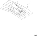
- Fig. 6 and 7 show an antenna assembly 1 with one or more antenna elements on the roof 2 of a vehicle 3 (e.g. a passenger car or truck or bus).
- a vehicle 3 e.g. a passenger car or truck or bus.
- Fig. 1 and Fig. 2 each respectively are a schematic illustration of an embodiment of an inventive antenna assembly 1 (e.g. for a roof 2 of a vehicle 3), comprising:
- Fig. 2 shows a schematic illustration of an embodiment of an inventive antenna assembly 1, wherein the printed circuit board 4 comprises two layers 14, 15, each with a top side 12; 17 and bottom side 18; 19 (wherein 12 here is the upper side 5 of the PCB and the upper side 12 of the top layer of the PCB).
- the feed connection pad 7 is capacitively coupled (through one layer 14 of the printed circuit board 4) to a (dotted) feedline pad 9 of the printed circuit board 4
- the ground connection pad 8 is capacitively coupled (through one layer 14 of the printed circuit board 4) to a (dotted) ground line pad 10 of the printed circuit board 4.
- the feedline pad 9 of the printed circuit board 4 is opposite to the feed connection pad 7 of the antenna element 11, and the ground line pad 10 of the printed circuit board 4 is opposite to the ground connection pad 8 of the antenna element 11 ('opposite" meaning on opposite sides of one layer 14 of the printed circuit board 4). So the feedline pad 9 and the groundline pad 10 are in the area of the feed connection pad 7 and the ground connection pad 8, fully or partially overlapping.
- the feed line 13 for the antenna element 11 comprises enlarged area at its ends forming the feedline pad 9 and the groundline pad 10 is a defined surface directly connected to rest of the ground and to the other ground layers while using vias e.g. 16 In the embodiment in Fig.
- the printed circuit board 4 is without copper metallization where the antenna feeding pin and the grounding pin is touching the PCB (top or bottom layer), especially to avoid electrical galvanic contact of the feed connection pad 7 and the ground connection pad 8 with the printed circuit board 4.
- the antenna assembly 11 comprises at least one screw 22, 23 for fixing of the antenna element 11 on the printed circuit board 4 by fastening the screw(s) 22, 23 through a housing 21 that holds the antenna element 11 and goes through the printed circuit board 4, especially with no electrical contact between the at least one screw 22, 23 and the antenna element 11, preferably pressing the feed connection pad 7 and the ground connection pad 8 of the antenna element 11 onto the printed circuit board 4.
- the antenna element 11 can e.g. comprise a conductive metal sheet and/or it can be a PIFA or IFA antenna element.
- the antenna assembly 1 can comprise one antenna element 11 or two or more antenna elements for cellular mobile communication and/or for WiFi communication and/or for a satellite positioning system and or for further purposes.
- Embodiments of the invention can avoid high cost given by possible alternative implementation/mounting processes, in which a classic metallic IFA or PIFA structure antenna has to be fixed in the plastic housing and also soldered on the mainboard to ensure an electrical contact with the corresponding circuit.
- Embodiments of the invention are proposing an idea for the implementation of an antenna in telephony systems which addresses the problems mentioned above. This can still allow using a PIFA design, but a difference consists in the fact that the antenna feed and ground connections do not need to be galvanically connected anymore to the associated electrical circuit connections. Both feed and ground pins of the antenna can only be capacitively coupled to the electronic circuit inputs without any galvanic contact. This can mean that there is no press-fit or soldering needed and, also, no possibility of imperfect electrical contact or corrosion during time.
- An antenna element 11 of the antenna assembly 1 can be is realized out of conductive metal sheet in the form of a PIFA structure with one feeding pin (with feed connection pad 7) and one grounding pin (with ground connection pad 8).
- the antenna element's multiple resonances to cover the needed multi-bands for telephony services can be realized by making slots on the upper and lateral surface of the metal sheet element.
- Both the feeding and the grounding pins are ended by enlarged pads 7, 8, parallel to the PCB 4 surface.
- These pads 7, 8 will be placed directly on the (when mounted) upper surface 5 of the PCB that here contains electronic circuit for a telephony system, but in the areas 24, 25 surrounding these two pads 7, 8 there is no copper metallization, therefore no electrical contact (of the pads 7, 8 with the printed circuit board 4).
- the feed and ground strip-lines 16, 17 for a telephone antenna 11 are routed.
- the antenna assembly 1 can be fixed in a plastic housing in a few plastic hot-melted points, then the complete housing can be pressed on the printed circuit board 4 with screws 22, 23 e. g in four corners, from which e.g. one of them can be going through the antenna ground pin (e.g. through the pad 8).
- the antenna feeding pin (pad 7) can be held in place and pressed onto the printed circuit board 4 by a housing shoulder behind it.
- FIG. 4 shows an input reflection coefficient of the antenna without matching in a simulation.
- Fig. 5 shows an input reflection coefficient and efficiency of the antenna with matching in a measurement.
- the presented result data is showing very good performance for the desired frequency bands, both in overall (S11) and radiation efficiency. Also, from the radiation pattern measurements, a total gain with a good behavior was obtained, quasi-omnidirectional on the entire frequency range.
- the described embodiments of the invention can be successfully implemented in real life, delivering the required performance in automotive telephony products.
- the design can be, of course, extended to other services, by changing the dimensions of the antenna elements and adapting the frequency bands.
Landscapes
- Engineering & Computer Science (AREA)
- Remote Sensing (AREA)
- Details Of Aerials (AREA)
Abstract
Description
- The invention concerns an antenna assembly and a vehicle.
- Antenna assemblies for cars are e. g. known from
EP2466552B1 , which concerns an antenna assembly with a PIFA antenna connected to a PCB. - It is an object of the invention to provide an improved antenna assembly.
The object is achieved by the subject matter of the independent claims respectively. Advantageous developments of the invention are found in the dependent claims. - According to the invention, an antenna assembly, especially for a vehicle, comprises:
- a printed circuit board having a top side and a bottom side and inbetween many internal layers ,
- at least one antenna element comprising a feed connection pad and a ground connection pad,
- the antenna element being arranged on (one side of) the printed circuit board, (which preferably is the antenna side),
- wherein (especially on that said printed circuit board side) the feed connection pad and the ground connection pad of the antenna element are located on the surface of the printed circuit board,
- wherein the feed connection pad is coupled to a feedline pad of the printed circuit board,
- The antenna feed and ground connections do not need to be galvanically connected to the associated electrical circuit connections on a printed circuit board. Both feed and ground pins of the antenna can only be capacitively coupled to the electronic circuit inputs of a printed circuit board without any galvanic contact. Press-fit or soldering are not necessary and, also, no possibility of imperfect electrical contact or corrosion during time should occur.
- According to the dependent patent claims, the invention also comprises embodiments that provide features which afford additional technical advantages.
- Preferably, the antenna assembly is comprising on the underside of one layer of the printed circuit board
- a (PCB) feed line with a feedline pad opposite to the (antenna) feed connection pad,
- a (PCB) ground line with a groundline pad opposite to the (antenna) ground line pad,
- Preferably for supporting capacitive coupling,
the (PCB) feedline pad and the (PCB) groundline pad are in the area of the (antenna) feed connection pad and the (antenna) ground connection pad. - Preferably, in the area of the feed connection pad and the ground connection pad where the antenna feeding pin and the grounding pin is touching the PCB (top or bottom layer),
the printed circuit board is without (copper) metallization,
especially to avoid electrical galvanic contact of the feed connection pad and the ground connection pad with the printed circuit board,
which electrical galvanic contact is not necessary due to capacitive (and/or inductive) coupling. - According to a further embodiment,
the (PCB) feedline pad and the (PCB) groundline pad are located on the side opposite to the antenna side of the printed circuit board preferably on an inner layer, which also contains an electronic circuit for at least one telecommunication and/or telephony system. - According to a further embodiment,
the antenna assembly comprises at least one screw for fixing of the antenna element on the printed circuit board by fastening the screw through a housing that holds the antenna element and goes through the printed circuit board, especially with no electrical contact between the screw and the antenna element,
preferably pressing the feed connection pad and the ground connection pad of the antenna element onto the printed circuit board. - According to a further embodiment, the antenna element comprises preferably a conductive metal sheet and/or is a PIFA or IFA antenna element.
According to a further embodiment, the antenna assembly comprises at least one antenna element for cellular mobile communication and/or for WiFi communication and/or for a satellite positioning system. - The invention also provides a vehicle comprising an antenna assembly.
- The invention also comprises the combinations of the features of the described embodiments.
- In the following an exemplary implementation of the invention is described.
The figures show in: -
Fig. 1 a schematic illustration of an embodiment of an inventive antenna assembly, -
Fig. 2 a schematic illustration of an embodiment of an inventive antenna assembly, -
Fig. 3 a schematic illustration of an embodiment of an inventive antenna assembly, with a housing and screws for fixing the antenna element on the printed circuit board, -
Fig. 4 an input reflection coefficient of an antenna without matching in a simulation, -
Fig. 5 an input reflection coefficient and efficiency of an antenna with matching in a measurement, -
Fig. 6 a roof of a vehicle with an antenna assembly, -
Fig. 7 a vehicle with an antenna assembly on its roof. - The embodiment explained in the following is a preferred embodiment of the invention. However, in the embodiment, the described components of the embodiment each represent individual features of the invention which are to be considered independently of each other and which each develop the invention also independently of each other and thereby are also to be regarded as a component of the invention in individual manner or in another than the shown combination. Furthermore, the described embodiment can also be supplemented by further features of the invention already described. In the figures elements that provide the same function are marked with identical reference signs.
-
Fig. 6 and7 show anantenna assembly 1 with one or more antenna elements on theroof 2 of a vehicle 3 (e.g. a passenger car or truck or bus). -
Fig. 1 andFig. 2 each respectively are a schematic illustration of an embodiment of an inventive antenna assembly 1 (e.g. for aroof 2 of a vehicle 3), comprising: - a printed circuit board (PCB) 4 having a
top side 5 and abottom side 6, - at least one
antenna element 11 comprising a feed connection pad 7 (for feeding the antenna) and a ground connection pad 8 (for grounding the antenna), - the
antenna element 11 being arranged on one (antenna)side 5 of the antenna circuit board, (which is in the following called the antenna side 5), - wherein on that
antenna side 5 thefeed connection pad 7 and theground connection pad 8 of theantenna element 1 are located on thesurface 12 of oneside 5 of the printedcircuit board 4, - wherein the
feed connection pad 7 is capacitively coupled (through one layer of the printed circuit board 4) to a (dotted)feedline pad 9 of the printedcircuit board 4, and wherein theground connection pad 8 is capacitively coupled (through one layer of the printed circuit board 4) to a (dotted)ground line pad 10 of the printedcircuit board 4. -
Fig. 2 shows a schematic illustration of an embodiment of aninventive antenna assembly 1, wherein theprinted circuit board 4 comprises twolayers top side 12; 17 andbottom side 18; 19 (wherein 12 here is theupper side 5 of the PCB and theupper side 12 of the top layer of the PCB). - In
Fig. 2 , thefeed connection pad 7 is capacitively coupled (through onelayer 14 of the printed circuit board 4) to a (dotted)feedline pad 9 of the printedcircuit board 4, and theground connection pad 8 is capacitively coupled (through onelayer 14 of the printed circuit board 4) to a (dotted)ground line pad 10 of the printedcircuit board 4. - The
feedline pad 9 of the printedcircuit board 4 is opposite to thefeed connection pad 7 of theantenna element 11,
and theground line pad 10 of the printedcircuit board 4 is opposite to theground connection pad 8 of the antenna element 11 ('opposite" meaning on opposite sides of onelayer 14 of the printed circuit board 4).
So thefeedline pad 9 and thegroundline pad 10 are in the area of thefeed connection pad 7 and theground connection pad 8, fully or partially overlapping.
In the embodiment inFig. 2 , thefeed line 13 for theantenna element 11 comprises enlarged area at its ends forming thefeedline pad 9 and thegroundline pad 10 is a defined surface directly connected to rest of the ground and to the other ground layers while using vias e.g. 16
In the embodiment inFig. 2 , in the area of thefeed connection pad 7 and theground connection pad 8, the printedcircuit board 4 is without copper metallization where the antenna feeding pin and the grounding pin is touching the PCB (top or bottom layer), especially to avoid electrical galvanic contact of thefeed connection pad 7 and theground connection pad 8 with the printedcircuit board 4.
In the embodiment inFig. 3 , theantenna assembly 11 comprises at least onescrew antenna element 11 on the printedcircuit board 4 by fastening the screw(s) 22, 23 through ahousing 21 that holds theantenna element 11 and goes through the printedcircuit board 4, especially with no electrical contact between the at least onescrew antenna element 11,
preferably pressing thefeed connection pad 7 and theground connection pad 8 of theantenna element 11 onto the printedcircuit board 4.
Theantenna element 11 can e.g. comprise a conductive metal sheet and/or it can be a PIFA or IFA antenna element.
According to an embodiment, theantenna assembly 1 can comprise oneantenna element 11 or two or more antenna elements for cellular mobile communication and/or for WiFi communication and/or for a satellite positioning system and or for further purposes. - Embodiments of the invention can avoid high cost given by possible alternative implementation/mounting processes, in which a classic metallic IFA or PIFA structure antenna has to be fixed in the plastic housing and also soldered on the mainboard to ensure an electrical contact with the corresponding circuit. Embodiments of the invention are proposing an idea for the implementation of an antenna in telephony systems which addresses the problems mentioned above. This can still allow using a PIFA design, but a difference consists in the fact that the antenna feed and ground connections do not need to be galvanically connected anymore to the associated electrical circuit connections. Both feed and ground pins of the antenna can only be capacitively coupled to the electronic circuit inputs without any galvanic contact. This can mean that there is no press-fit or soldering needed and, also, no possibility of imperfect electrical contact or corrosion during time.
- An
antenna element 11 of theantenna assembly 1 can be is realized out of conductive metal sheet in the form of a PIFA structure with one feeding pin (with feed connection pad 7) and one grounding pin (with ground connection pad 8). - The antenna element's multiple resonances to cover the needed multi-bands for telephony services can be realized by making slots on the upper and lateral surface of the metal sheet element. Both the feeding and the grounding pins are ended by
enlarged pads PCB 4 surface. Thesepads upper surface 5 of the PCB that here contains electronic circuit for a telephony system, but in theareas pads pads lines 16, 17 for atelephone antenna 11 are routed. The shape of these lines is here also ending by enlarged areas, e.g. exactly below the antenna pads. By this method, a very strong capacitively electromagnetic coupling can be insured between antenna pins /pads - In order to ensure a good signal transfer between the antenna and the PCB (printed circuit board 4) traces on
lower PCB layer 15, the distance of the prepreg material between the upper PCB layer 14 (e.g. top layer) and lower PCB layer 15 (e.g. signal Layer) can be small (e.g. d = 90 to 100 microns).
Theantenna assembly 1 can be fixed in a plastic housing in a few plastic hot-melted points, then the complete housing can be pressed on the printedcircuit board 4 withscrews circuit board 4 by a housing shoulder behind it.
Some simulation and measurement results on a prototype realized for multi-band telephony services (700-960MHz, 1447-1511MHz, 1710-2170MHz & 2490-2690MHz) are presented inFig. 4 andFig. 5 .
Figure 4 shows an input reflection coefficient of the antenna without matching in a simulation.
Fig. 5 shows an input reflection coefficient and efficiency of the antenna with matching in a measurement.
The presented result data is showing very good performance for the desired frequency bands, both in overall (S11) and radiation efficiency. Also, from the radiation pattern measurements, a total gain with a good behavior was obtained, quasi-omnidirectional on the entire frequency range.
The described embodiments of the invention can be successfully implemented in real life, delivering the required performance in automotive telephony products. The design can be, of course, extended to other services, by changing the dimensions of the antenna elements and adapting the frequency bands. Some main advantages of this invention are the ease of fabrication and mounting, reduced assembly steps and shorter time spent during on the production process. -
- 1 antenna assembly
- 2 roof
- 3 vehicle
- 4 printed circuit board (PCB)
- 5 (PCB) top side
- 6 (PCB) underside
- 7 (antenna) feed connection pad
- 8 (antenna) ground connection pad
- 9 (PCB) feedline pad
- 10 (PCB) ground line pad
- 11 antenna element
- 12 upper side of (PCB) layer and PCB
- 13 feed line
- 14 (PCB) layer
- 15 (PCB) layer
- 16 ground line
- 17 upper side of (PCB) layer
- 18 underside of (PCB) layer and PCB
- 19 underside of (PCB) layer
- 21 housing
- 22 screw
- 23 screw
Claims (11)
- An antenna assembly (1), especially for a vehicle, comprising:- a printed circuit board (4),- at least one antenna element (11) comprising a feed connection pad (7) and a ground connection pad (8),- the antenna element (11) being arranged on the printed circuit board (4),- wherein the feed connection pad (7) and the ground connection pad (8) of the antenna element (1) each are located on a surface (12) of the printed circuit board (4),- wherein the feed connection pad (7) is coupled to a feedline pad (9) of the printed circuit board (4),and wherein the ground connection pad (8) is coupled to a ground line pad (10) of the printed circuit board (4).
- Antenna assembly (1) according to the preceding claim,
wherein the feedline pad (9) is capacitively coupled to the feed connection pad (7),
wherein the groundline pad (10) is capacitively coupled to the ground connection pad (8),
especially without galvanic and/or without direct electrical connection between the antenna element (11) or feed connection pad (7) or ground connection pad (8) and the printed circuit board (4). - Antenna assembly (1) according to any of the preceding claims,
wherein the printed circuit board (4), having a top side (5) and a bottom side (6), has at least two layers (14, 15), each with two layer surfaces (17, 18, 19, 20), wherein a layer surface, especially a layer (17) surface with the smallest distance (d) to the antenna side (5) surface (12), comprises- a feed line (13) with a feedline pad (9) opposite to the feed connection pad (7),- a ground line (16) with a ground line pad (10) opposite to the ground connection pad (8). - Antenna assembly (1) according to any of the preceding claims,
wherein the feed line (13) and the ground line (16) for the antenna element (11) respectively comprise enlarged areas at their ends,
respectively forming the feedline pad (9) and the groundline pad (10). - Antenna assembly (1) according to any of the preceding claims,
wherein the feedline pad (9) and the groundline pad (10)
are fully or partially overlapping in the area of the feed connection pad (7) and the ground connection pad (8) - Antenna assembly (1) according to any of the preceding claims,
wherein in the area of the feed connection pad (7) and the ground connection pad (8),
the printed circuit board (4) is without copper metallization,
especially to avoid electrical galvanic contact of the feed connection pad (7) and the ground connection pad (8) with the printed circuit board (4). - Antenna assembly (1) according to any of the preceding claims,
wherein the feedline pad (9) and the groundline pad (10) are located on the printed circuit boards (4) side (18) opposite to the antenna element side (12) of the printed circuit board (4), which (18) also contains an electronic circuit for at least one telecommunication and/or telephony system. - Antenna assembly (1) according to any of the preceding claims,
wherein the antenna assembly (11) comprises at least one screw (22,23) for fixing of the antenna element (11) on the printed circuit board (4) by fastening the screw (22, 23) through a housing (21) that holds the antenna element (11) and goes through the printed circuit board (4),
especially with no electrical contact between the screw (23) and the antenna element (11),
preferably pressing the feed connection pad (7) and the ground connection pad (8) of the antenna element (11) onto the printed circuit board (4). - Antenna assembly (1) according to any of the preceding claims,
wherein the antenna element (11) comprises a conductive metal sheet and/or is a PIFA or IFA antenna element. - Antenna assembly (1) according to any of the preceding claims,
wherein it comprises at least one antenna element (11) for cellular mobile communication and/or for WiFi communication and/or for a satellite positioning system. - Vehicle, especially car or truck,
with an antenna assembly (1) according to any of the preceding claims.
Priority Applications (1)
| Application Number | Priority Date | Filing Date | Title |
|---|---|---|---|
| EP21465517.7A EP4071930B1 (en) | 2021-04-08 | 2021-04-08 | Antenna assembly and vehicle |
Applications Claiming Priority (1)
| Application Number | Priority Date | Filing Date | Title |
|---|---|---|---|
| EP21465517.7A EP4071930B1 (en) | 2021-04-08 | 2021-04-08 | Antenna assembly and vehicle |
Publications (2)
| Publication Number | Publication Date |
|---|---|
| EP4071930A1 true EP4071930A1 (en) | 2022-10-12 |
| EP4071930B1 EP4071930B1 (en) | 2025-08-20 |
Family
ID=75887982
Family Applications (1)
| Application Number | Title | Priority Date | Filing Date |
|---|---|---|---|
| EP21465517.7A Active EP4071930B1 (en) | 2021-04-08 | 2021-04-08 | Antenna assembly and vehicle |
Country Status (1)
| Country | Link |
|---|---|
| EP (1) | EP4071930B1 (en) |
Citations (7)
| Publication number | Priority date | Publication date | Assignee | Title |
|---|---|---|---|---|
| US20050001768A1 (en) * | 2003-05-29 | 2005-01-06 | Masami Sekiguchi | Surface mount antenna, and an antenna element mounting method |
| US20050093678A1 (en) * | 2003-11-04 | 2005-05-05 | Forster Ian J. | RFID tag with enhanced readability |
| US20060192712A1 (en) * | 2005-02-25 | 2006-08-31 | Samsung Electro-Mechanics Co., Ltd. | Antenna module and electronic device using the same |
| US20090015497A1 (en) * | 2006-02-14 | 2009-01-15 | Murata Manufacturing Co., Ltd | Antenna structure and wireless communication apparatus including same |
| US20090033570A1 (en) * | 2007-07-30 | 2009-02-05 | High Tech Computer Corp. | Antenna module and electronic device using the same |
| EP2466552B1 (en) | 2010-12-20 | 2018-07-25 | Continental Automotive GmbH | On-board information system with mobile radio antenna |
| DE102017010514A1 (en) * | 2017-11-10 | 2019-05-16 | Heinz Lindenmeier | Reception antenna for satellite navigation on a vehicle |
-
2021
- 2021-04-08 EP EP21465517.7A patent/EP4071930B1/en active Active
Patent Citations (7)
| Publication number | Priority date | Publication date | Assignee | Title |
|---|---|---|---|---|
| US20050001768A1 (en) * | 2003-05-29 | 2005-01-06 | Masami Sekiguchi | Surface mount antenna, and an antenna element mounting method |
| US20050093678A1 (en) * | 2003-11-04 | 2005-05-05 | Forster Ian J. | RFID tag with enhanced readability |
| US20060192712A1 (en) * | 2005-02-25 | 2006-08-31 | Samsung Electro-Mechanics Co., Ltd. | Antenna module and electronic device using the same |
| US20090015497A1 (en) * | 2006-02-14 | 2009-01-15 | Murata Manufacturing Co., Ltd | Antenna structure and wireless communication apparatus including same |
| US20090033570A1 (en) * | 2007-07-30 | 2009-02-05 | High Tech Computer Corp. | Antenna module and electronic device using the same |
| EP2466552B1 (en) | 2010-12-20 | 2018-07-25 | Continental Automotive GmbH | On-board information system with mobile radio antenna |
| DE102017010514A1 (en) * | 2017-11-10 | 2019-05-16 | Heinz Lindenmeier | Reception antenna for satellite navigation on a vehicle |
Also Published As
| Publication number | Publication date |
|---|---|
| EP4071930B1 (en) | 2025-08-20 |
Similar Documents
| Publication | Publication Date | Title |
|---|---|---|
| KR101044994B1 (en) | Antenna device of mobile terminal | |
| US7916086B2 (en) | Antenna component and methods | |
| US8810457B2 (en) | Orthogonal modular embedded antenna, with method of manufacture and kits therefor | |
| US10205216B2 (en) | Thin film antenna to FAKRA connector | |
| US9048543B2 (en) | Orthogonal modular embedded antenna, with method of manufacture and kits therefor | |
| KR20020011141A (en) | Integrable dual-band antenna | |
| CN110098480B (en) | Chip antenna and antenna module comprising same | |
| CN106450661A (en) | Antenna device, electronic apparatus, and method of mounting antenna device | |
| JPH10117108A (en) | Antenna device for wireless equipment | |
| CN103022637B (en) | A kind of built-in aerial, the mobile terminal of built-in aerial and communication means thereof | |
| US11355847B2 (en) | Antenna structure | |
| KR101265434B1 (en) | Antenna with built-in filter and electronic device | |
| JPWO2014103509A1 (en) | Circuit boards and electronic equipment | |
| CN102170043B (en) | A kind of wireless terminal and antenna thereof | |
| US12003026B2 (en) | Antenna device and vehicle comprising an antenna device | |
| KR102239231B1 (en) | Combo antenna module and manufacturing method thereof | |
| EP4071930B1 (en) | Antenna assembly and vehicle | |
| US10090590B2 (en) | Apparatus and methods for antenna port isolation | |
| JP3374604B2 (en) | Wireless communication device | |
| US20120287015A1 (en) | Multi-layer antenna | |
| KR20090099235A (en) | Antenna structure | |
| US9893420B2 (en) | Wireless module with plural in-plane terminals | |
| CN101127414B (en) | Method for increasing equivalent height of PIFA antenna device | |
| EP4546564A1 (en) | A full band cellular antenna | |
| EP4518020A1 (en) | Support component for an antenna on a pcb |
Legal Events
| Date | Code | Title | Description |
|---|---|---|---|
| PUAI | Public reference made under article 153(3) epc to a published international application that has entered the european phase |
Free format text: ORIGINAL CODE: 0009012 |
|
| STAA | Information on the status of an ep patent application or granted ep patent |
Free format text: STATUS: THE APPLICATION HAS BEEN PUBLISHED |
|
| AK | Designated contracting states |
Kind code of ref document: A1 Designated state(s): AL AT BE BG CH CY CZ DE DK EE ES FI FR GB GR HR HU IE IS IT LI LT LU LV MC MK MT NL NO PL PT RO RS SE SI SK SM TR |
|
| STAA | Information on the status of an ep patent application or granted ep patent |
Free format text: STATUS: REQUEST FOR EXAMINATION WAS MADE |
|
| 17P | Request for examination filed |
Effective date: 20230412 |
|
| RBV | Designated contracting states (corrected) |
Designated state(s): AL AT BE BG CH CY CZ DE DK EE ES FI FR GB GR HR HU IE IS IT LI LT LU LV MC MK MT NL NO PL PT RO RS SE SI SK SM TR |
|
| RAP3 | Party data changed (applicant data changed or rights of an application transferred) |
Owner name: CONTINENTAL AUTOMOTIVE TECHNOLOGIES GMBH |
|
| GRAP | Despatch of communication of intention to grant a patent |
Free format text: ORIGINAL CODE: EPIDOSNIGR1 |
|
| STAA | Information on the status of an ep patent application or granted ep patent |
Free format text: STATUS: GRANT OF PATENT IS INTENDED |
|
| RIC1 | Information provided on ipc code assigned before grant |
Ipc: H01Q 9/42 20060101ALN20250220BHEP Ipc: H01Q 1/38 20060101ALI20250220BHEP Ipc: H01Q 1/48 20060101ALI20250220BHEP Ipc: H01Q 9/04 20060101ALI20250220BHEP Ipc: H01Q 1/32 20060101AFI20250220BHEP |
|
| INTG | Intention to grant announced |
Effective date: 20250311 |
|
| GRAS | Grant fee paid |
Free format text: ORIGINAL CODE: EPIDOSNIGR3 |
|
| GRAA | (expected) grant |
Free format text: ORIGINAL CODE: 0009210 |
|
| STAA | Information on the status of an ep patent application or granted ep patent |
Free format text: STATUS: THE PATENT HAS BEEN GRANTED |
|
| AK | Designated contracting states |
Kind code of ref document: B1 Designated state(s): AL AT BE BG CH CY CZ DE DK EE ES FI FR GB GR HR HU IE IS IT LI LT LU LV MC MK MT NL NO PL PT RO RS SE SI SK SM TR |
|
| REG | Reference to a national code |
Ref country code: GB Ref legal event code: FG4D |
|
| REG | Reference to a national code |
Ref country code: CH Ref legal event code: EP |
|
| REG | Reference to a national code |
Ref country code: DE Ref legal event code: R096 Ref document number: 602021036572 Country of ref document: DE |
|
| REG | Reference to a national code |
Ref country code: IE Ref legal event code: FG4D |
|
| REG | Reference to a national code |
Ref country code: CH Ref legal event code: W10 Free format text: ST27 STATUS EVENT CODE: U-0-0-W10-W00 (AS PROVIDED BY THE NATIONAL OFFICE) Effective date: 20251022 |
|
| RAP4 | Party data changed (patent owner data changed or rights of a patent transferred) |
Owner name: AUMOVIO GERMANY GMBH |
|
| REG | Reference to a national code |
Ref country code: NL Ref legal event code: MP Effective date: 20250820 |
|
| PG25 | Lapsed in a contracting state [announced via postgrant information from national office to epo] |
Ref country code: IS Free format text: LAPSE BECAUSE OF FAILURE TO SUBMIT A TRANSLATION OF THE DESCRIPTION OR TO PAY THE FEE WITHIN THE PRESCRIBED TIME-LIMIT Effective date: 20251220 |
|
| PG25 | Lapsed in a contracting state [announced via postgrant information from national office to epo] |
Ref country code: NO Free format text: LAPSE BECAUSE OF FAILURE TO SUBMIT A TRANSLATION OF THE DESCRIPTION OR TO PAY THE FEE WITHIN THE PRESCRIBED TIME-LIMIT Effective date: 20251120 |
|
| REG | Reference to a national code |
Ref country code: LT Ref legal event code: MG9D |
|
| PG25 | Lapsed in a contracting state [announced via postgrant information from national office to epo] |
Ref country code: PT Free format text: LAPSE BECAUSE OF FAILURE TO SUBMIT A TRANSLATION OF THE DESCRIPTION OR TO PAY THE FEE WITHIN THE PRESCRIBED TIME-LIMIT Effective date: 20251222 |
|
| PG25 | Lapsed in a contracting state [announced via postgrant information from national office to epo] |
Ref country code: FI Free format text: LAPSE BECAUSE OF FAILURE TO SUBMIT A TRANSLATION OF THE DESCRIPTION OR TO PAY THE FEE WITHIN THE PRESCRIBED TIME-LIMIT Effective date: 20250820 |
|
| PG25 | Lapsed in a contracting state [announced via postgrant information from national office to epo] |
Ref country code: HR Free format text: LAPSE BECAUSE OF FAILURE TO SUBMIT A TRANSLATION OF THE DESCRIPTION OR TO PAY THE FEE WITHIN THE PRESCRIBED TIME-LIMIT Effective date: 20250820 Ref country code: NL Free format text: LAPSE BECAUSE OF FAILURE TO SUBMIT A TRANSLATION OF THE DESCRIPTION OR TO PAY THE FEE WITHIN THE PRESCRIBED TIME-LIMIT Effective date: 20250820 |
|
| PG25 | Lapsed in a contracting state [announced via postgrant information from national office to epo] |
Ref country code: GR Free format text: LAPSE BECAUSE OF FAILURE TO SUBMIT A TRANSLATION OF THE DESCRIPTION OR TO PAY THE FEE WITHIN THE PRESCRIBED TIME-LIMIT Effective date: 20251121 |
|
| PG25 | Lapsed in a contracting state [announced via postgrant information from national office to epo] |
Ref country code: SE Free format text: LAPSE BECAUSE OF FAILURE TO SUBMIT A TRANSLATION OF THE DESCRIPTION OR TO PAY THE FEE WITHIN THE PRESCRIBED TIME-LIMIT Effective date: 20250820 |
|
| PG25 | Lapsed in a contracting state [announced via postgrant information from national office to epo] |
Ref country code: LV Free format text: LAPSE BECAUSE OF FAILURE TO SUBMIT A TRANSLATION OF THE DESCRIPTION OR TO PAY THE FEE WITHIN THE PRESCRIBED TIME-LIMIT Effective date: 20250820 |
|
| PG25 | Lapsed in a contracting state [announced via postgrant information from national office to epo] |
Ref country code: PL Free format text: LAPSE BECAUSE OF FAILURE TO SUBMIT A TRANSLATION OF THE DESCRIPTION OR TO PAY THE FEE WITHIN THE PRESCRIBED TIME-LIMIT Effective date: 20250820 Ref country code: BG Free format text: LAPSE BECAUSE OF FAILURE TO SUBMIT A TRANSLATION OF THE DESCRIPTION OR TO PAY THE FEE WITHIN THE PRESCRIBED TIME-LIMIT Effective date: 20250820 |
|
| REG | Reference to a national code |
Ref country code: DE Ref legal event code: R081 Ref document number: 602021036572 Country of ref document: DE Owner name: AUMOVIO GERMANY GMBH, DE Free format text: FORMER OWNER: CONTINENTAL AUTOMOTIVE TECHNOLOGIES GMBH, 30175 HANNOVER, DE |
|
| PG25 | Lapsed in a contracting state [announced via postgrant information from national office to epo] |
Ref country code: RS Free format text: LAPSE BECAUSE OF FAILURE TO SUBMIT A TRANSLATION OF THE DESCRIPTION OR TO PAY THE FEE WITHIN THE PRESCRIBED TIME-LIMIT Effective date: 20251120 |
|
| PG25 | Lapsed in a contracting state [announced via postgrant information from national office to epo] |
Ref country code: ES Free format text: LAPSE BECAUSE OF FAILURE TO SUBMIT A TRANSLATION OF THE DESCRIPTION OR TO PAY THE FEE WITHIN THE PRESCRIBED TIME-LIMIT Effective date: 20250820 |
|
| REG | Reference to a national code |
Ref country code: AT Ref legal event code: MK05 Ref document number: 1828376 Country of ref document: AT Kind code of ref document: T Effective date: 20250820 |
|
| PG25 | Lapsed in a contracting state [announced via postgrant information from national office to epo] |
Ref country code: SM Free format text: LAPSE BECAUSE OF FAILURE TO SUBMIT A TRANSLATION OF THE DESCRIPTION OR TO PAY THE FEE WITHIN THE PRESCRIBED TIME-LIMIT Effective date: 20250820 |
|
| PGFP | Annual fee paid to national office [announced via postgrant information from national office to epo] |
Ref country code: GB Payment date: 20260313 Year of fee payment: 6 |
|
| PG25 | Lapsed in a contracting state [announced via postgrant information from national office to epo] |
Ref country code: DK Free format text: LAPSE BECAUSE OF FAILURE TO SUBMIT A TRANSLATION OF THE DESCRIPTION OR TO PAY THE FEE WITHIN THE PRESCRIBED TIME-LIMIT Effective date: 20250820 |
|
| PG25 | Lapsed in a contracting state [announced via postgrant information from national office to epo] |
Ref country code: AT Free format text: LAPSE BECAUSE OF FAILURE TO SUBMIT A TRANSLATION OF THE DESCRIPTION OR TO PAY THE FEE WITHIN THE PRESCRIBED TIME-LIMIT Effective date: 20250820 |
|
| PG25 | Lapsed in a contracting state [announced via postgrant information from national office to epo] |
Ref country code: CZ Free format text: LAPSE BECAUSE OF FAILURE TO SUBMIT A TRANSLATION OF THE DESCRIPTION OR TO PAY THE FEE WITHIN THE PRESCRIBED TIME-LIMIT Effective date: 20250820 |
|
| PG25 | Lapsed in a contracting state [announced via postgrant information from national office to epo] |
Ref country code: SK Free format text: LAPSE BECAUSE OF FAILURE TO SUBMIT A TRANSLATION OF THE DESCRIPTION OR TO PAY THE FEE WITHIN THE PRESCRIBED TIME-LIMIT Effective date: 20250820 Ref country code: EE Free format text: LAPSE BECAUSE OF FAILURE TO SUBMIT A TRANSLATION OF THE DESCRIPTION OR TO PAY THE FEE WITHIN THE PRESCRIBED TIME-LIMIT Effective date: 20250820 |
|
| REG | Reference to a national code |
Ref country code: DE Ref legal event code: R097 Ref document number: 602021036572 Country of ref document: DE |
|
| PLBE | No opposition filed within time limit |
Free format text: ORIGINAL CODE: 0009261 |
|
| STAA | Information on the status of an ep patent application or granted ep patent |
Free format text: STATUS: NO OPPOSITION FILED WITHIN TIME LIMIT |
|
| PG25 | Lapsed in a contracting state [announced via postgrant information from national office to epo] |
Ref country code: LT Free format text: LAPSE BECAUSE OF FAILURE TO SUBMIT A TRANSLATION OF THE DESCRIPTION OR TO PAY THE FEE WITHIN THE PRESCRIBED TIME-LIMIT Effective date: 20250820 |
|
| REG | Reference to a national code |
Ref country code: CH Ref legal event code: L10 Free format text: ST27 STATUS EVENT CODE: U-0-0-L10-L00 (AS PROVIDED BY THE NATIONAL OFFICE) Effective date: 20260701 |
|
| PGFP | Annual fee paid to national office [announced via postgrant information from national office to epo] |
Ref country code: IT Payment date: 20260422 Year of fee payment: 6 |
|
| PGFP | Annual fee paid to national office [announced via postgrant information from national office to epo] |
Ref country code: DE Payment date: 20260430 Year of fee payment: 6 |
|
| PGFP | Annual fee paid to national office [announced via postgrant information from national office to epo] |
Ref country code: FR Payment date: 20260423 Year of fee payment: 6 |
|
| 26N | No opposition filed |
Effective date: 20260521 |