EP4071784A1 - Ionenquelle für gepulsten elektronenionisierungsprozesse - Google Patents
Ionenquelle für gepulsten elektronenionisierungsprozesse Download PDFInfo
- Publication number
- EP4071784A1 EP4071784A1 EP22174694.4A EP22174694A EP4071784A1 EP 4071784 A1 EP4071784 A1 EP 4071784A1 EP 22174694 A EP22174694 A EP 22174694A EP 4071784 A1 EP4071784 A1 EP 4071784A1
- Authority
- EP
- European Patent Office
- Prior art keywords
- filament
- voltage
- ion
- electron
- supply
- Prior art date
- Legal status (The legal status is an assumption and is not a legal conclusion. Google has not performed a legal analysis and makes no representation as to the accuracy of the status listed.)
- Pending
Links
Images





Classifications
-
- H—ELECTRICITY
- H01—ELECTRIC ELEMENTS
- H01J—ELECTRIC DISCHARGE TUBES OR DISCHARGE LAMPS
- H01J49/00—Particle spectrometers or separator tubes
- H01J49/02—Details
- H01J49/10—Ion sources; Ion guns
- H01J49/14—Ion sources; Ion guns using particle bombardment, e.g. ionisation chambers
- H01J49/147—Ion sources; Ion guns using particle bombardment, e.g. ionisation chambers with electrons, e.g. electron impact ionisation, electron attachment
-
- H—ELECTRICITY
- H01—ELECTRIC ELEMENTS
- H01J—ELECTRIC DISCHARGE TUBES OR DISCHARGE LAMPS
- H01J49/00—Particle spectrometers or separator tubes
- H01J49/02—Details
- H01J49/06—Electron- or ion-optical arrangements
- H01J49/067—Ion lenses, apertures, skimmers
-
- H—ELECTRICITY
- H01—ELECTRIC ELEMENTS
- H01J—ELECTRIC DISCHARGE TUBES OR DISCHARGE LAMPS
- H01J49/00—Particle spectrometers or separator tubes
- H01J49/02—Details
- H01J49/022—Circuit arrangements, e.g. for generating deviation currents or voltages ; Components associated with high voltage supply
-
- H—ELECTRICITY
- H01—ELECTRIC ELEMENTS
- H01J—ELECTRIC DISCHARGE TUBES OR DISCHARGE LAMPS
- H01J49/00—Particle spectrometers or separator tubes
- H01J49/02—Details
- H01J49/10—Ion sources; Ion guns
- H01J49/16—Ion sources; Ion guns using surface ionisation, e.g. field-, thermionic- or photo-emission
-
- H—ELECTRICITY
- H01—ELECTRIC ELEMENTS
- H01J—ELECTRIC DISCHARGE TUBES OR DISCHARGE LAMPS
- H01J49/00—Particle spectrometers or separator tubes
- H01J49/26—Mass spectrometers or separator tubes
Definitions
- the present disclosure is directed to the field of mass spectrometry. More particularly, the present disclosure relates to a mass spectrometer system and method that provides for improved electron ionization and measuring the effective emission current of an electron beam used for electron ionization.
- an ion trap mass spectrometer includes a ring electrode 11 and end caps 12 spaced from one another.
- An RF generator 14 applies an RF voltage to the ring electrode 11 to supply an RF voltage between the end caps 12 and the ring electrode 11 to provide a substantially quadrupole field for trapping ions in the ion volume 15 (or otherwise referred to herein as an "ion trap") between the end caps 12 and ring electrode 11.
- a supplementary RF generator 17 is coupled to the end caps 12 by the transformer 16 and supplies an axial RF voltage between the end caps 12.
- a heated filament 18 is held at a negative potential with respect to the ion trap DC or offset voltage.
- the electrons are gated into the ion volume 15 by a gate electrode 19 so that molecules or atoms are ionized in the interior of the ion volume 15 only during ionization of the sample molecules introduced into the ion volume 15.
- the amplitude of the fundamental RF voltage is scanned to bring successive ions formed in the ion volume 15 into resonance with the supplementary RF field, the ion trajectories increase until they exit from the perforated end cap 12 and are detected by continuous dynode electron multiplier.
- the electron multiplier converts the ion current into an electrical signal which is plotted as a function of time to provide a mass spectrum. Operation of ion trap mass spectrometers is described in U.S. Pat. No. 4,540,884, entitled “Method of Mass Analyzing a Sample by Use of a Quadrupole Ion Trap," issued September 10, 1985 , and U.S. Pat. No. 4,736,101, entitled “Method of Operating Ion Trap Detector in MS/MS Mode,” issued April 5, 1988 , wherein the disclosures of both patents are incorporated herein by reference.
- the electron multiplier can also produce electrical signals in a non-coherent manner during the period that the electron multiplier is energized. These signals are often referred to as "noise.”
- the noise signals produced come from two sources: 1) ions produced external to the trapping volume 15 by filament 18 produced electrons, and 2) ions resulting from excited neutral particles striking the surface of the ion volume 15. Since the filament 18 is typically operated at a high negative voltage potential, such as -70 electron volts (eV), electrons emitted by the filament 18 ionize gas molecules external to the ion volume 15.
- These electrons may not enter the ion volume 15 due to repulsion forces by the gate electrode 19, but the electrons can instead drift through the ion trap vacuum chamber 21.
- these ions reach the area of the electron multiplier, they are accelerated to the multiplier surface by the high negative voltage potential of the multiplier dynode and therefore they can generate noise signals.
- the helium molecules are bombarded by the energetic electrons, thereby producing positive helium ions in addition to excited neutral molecules. These energetic particles strike surfaces with sufficient energy to sputter off adsorbed molecules/atoms, and ions.
- Mass spectrometers employing electron ionization rely on emission current feedback or collector current feedback in order to close the loop on filament current.
- a rhenium or tungsten cathode filament is employed as the electron emitter and is heated to incandescence in order to affect thermionic emission from the surface of the wire.
- a separate bias supply is used to replenish electrons emitted into free space.
- FIGS. 2A-2B generally illustrate prior art methods for measuring and replenishing emitted electrons in accordance with emission current regulation and collector current regulation respectively.
- a filament 30 emits electrons past an opening in filament shroud 29, and through an opening in an electron lens 31 into an ion volume 32 through an opening 34 in the ion volume 32.
- Emitted electrons can be measured by measuring the potential drop across a feedback resistor 36 as part of a floating filament power supply 38.
- emitted electrons can be measured by an electron collector 40 on the opposite side of the ion volume 32 through electron exit aperture 42.
- the above measurement techniques are prone to measurement inaccuracies concerning the actual electron current delivered into the ion volume 32.
- a collector 40 used to measure electrons which traverse an ion volume 32 will not measure electrons impacting the near inner surface of the ion volume near the electron exit aperture 42.
- Embodiments of this disclosure provide improved systems and methods for emission current regulation of an electron beam used for continuous electron ionization and provides improvements for ions formed in pulsed electron ionization processes.
- an ion source assembly can include an electron source configured to inject electrons into an ion volume to ionize an atom or molecule in the ion volume, wherein the electron source can include a filament.
- the ion source assembly can further include a lens electrode positioned adjacent the electron source and having an opening, wherein the opening can be configured to pass electrons therethrough from the electron source into the ion volume.
- the ion source assembly can include a supply voltage source coupled to the filament, wherein the supply voltage source can be configured to supply a first voltage to the filament which is operable to ionize the molecules in the ion volume.
- the ion source can also include a bias voltage source coupled to the supply voltage source and configured to supply a bias voltage to the lens electrode, wherein the bias voltage can be configured to remain at a fixed voltage potential relative to the supply voltage source.
- an ion source assembly can include a filament configured to emit electrons via thermionic emission and a lens electrode surrounding the filament. Further, an ion source assembly can include a first power supply coupled to the filament, wherein the first power supply can be configured to supply a first voltage output at a first voltage slew rate to the filament. The first voltage output can be operable to ionize molecules. Still further, an ion source assembly can include a second power supply coupled to the lens electrode, wherein the second power supply can be configured to supply a second voltage output at a second voltage slew rate to the lens electrode.
- the ion source assembly can optionally include a first capacitor coupling the first voltage output to the second voltage output, and a resistor coupled between the second voltage output and the lens electrode.
- the first capacitor and the resistor can be operable to align the first voltage slew rate with the second voltage slew rate.
- the systems and methods disclosed can provide improved instrument-to-instrument repeatability in ion response, a decreased number of power supplies needed for pulsed-mode operation, and improved slew rate matching including a reduced or eliminated need for offset matching, thereby resulting in improved emission regulation in pulsed-emission mode.
- a “system” sets forth a set of components, real or abstract, comprising a whole where each component interacts with or is related to at least one other component within the whole.
- floating refers to a circuit, power supply, or other electrical feature which does not possess a ground which is common with earth ground.
- Conductors such as filaments and electron lenses, are also described as having a floating potential if they are connected electrically to another floating conductor.
- a filament power supply used to heat a filament to incandescence may supply a few amperes of current at only one or two volts across the filament. If the power supply does not have its ground in common with earth ground, the entire circuit can be said to "float” as its potential is not established.
- Establishing a potential can be accomplished by providing a bias voltage source which has its ground in common with earth ground.
- an electron lens is not floating if its power supply has its ground connected to earth ground but is floating if its ground is connected to another floated circuit such as a floated filament power supply.
- AGC Automatic Gain Control control methods for beam instruments are described in the '682 Patent, U.S. Pat. No. 7,507,954, entitled “Pulsed Ion Source for Quadrupole Mass Spectrometer Method,” issued March 24, 2009 , and U.S. Pat. No. 7,759,655, entitled “Pulsed Ion Source for Quadrupole Mass Spectrometer and Method,” issued July 20, 2010 , the disclosures of which are herein incorporated by reference.
- AGC for quadrupoles can control ion formation on a mass-to-mass basis while individual ions are being scanned by the multipole. This can be used to suppress non-target matrix ions for full scan experiments or prevent detector saturation for MRM experiments amongst other modes.
- the '996 Patent describes an electron gating scheme wherein a filament bias potential is switched between two different negative values. An electron lens potential is also switched between two different positive values. The switching is synchronized to happen at the same time, such that a constant potential difference is maintained between the filament and the electron lens. This allows the ability to turn the ionization process on and off without disruption of the emission regulation process. It requires four independent potentials and switching means for both channels. As such, the method and hardware employed in the '996 Patent synchronizes the gate times of the filament and electron lens. This results in the ability to gate the ionization process without unduly affecting the control (i.e., the precision) of emission current. This is largely due to the fact that the injection times are relatively long (e.g., within the millisecond time domain). The '996 Patent further describes systems which eliminate neutral noise formation during scan out of ions from an ion trap.
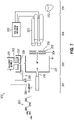
- a gas chromatograph 123 provides sample gas to an ion volume 124.
- An electron source 130 provides energetic electrons to the ion source to ionize the atoms and molecules in said device and form positive ions 125 and unwanted excited neutrals 126.
- the ions are guided or gated into the ion trap 129 by the multi-element lens L1, L2, and L3.
- the ion volume 124 and its operation is as described above.
- the ejected ions from the trap are converted to electrons by conversion dynode 127 and multiplied by the electron multiplier 128 which provides the output electrical signal representative of the ion abundance.
- the energy of the electrons leaving the filament 131 and entering the ion volume 124 is controlled so that it is sufficient to ionize sample molecules and helium 126 within the source volume 124 only during the ionization time.
- the electron source includes a filament 131 which is heated to emit electrons.
- the filament may comprise a refractory material such as tungsten, rhenium or another suitable alloy for thermionic emission.
- the heating current supplied to the filament 131 is from a floated power supply and is controlled to provide substantially constant electron emission.
- a filament shroud 132 is electrically common with filament 131 and assures that emission of electrons is at the opening 133.
- the energy of electrons entering the ion source volume 124 is controlled by the voltage between the filament 131 and the ion source volume 124. Seventy eV has been found to be an electron energy satisfactory for ionizing atoms and molecules, though higher or lower electron energies may be used.
- the filament voltage and/or excitation voltage is reduced to a voltage below the ionizing voltage for helium during nonionizing periods.
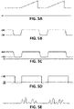
- FIG. 5A shows operation of the ion trap 129.
- the fundamental RF voltage is low as the ion trap is filled with sample ions.
- the voltage is then increased to provide a mass spectrum, FIG. 5E . Ions are formed and gated into the ion trap when the fundamental RF voltage is low.
- FIG. 5B shows the voltage applied to the filament 131 from a voltage source (not shown) during ionization and during analysis.
- the voltage is at minus 70 volts during ionization thereby providing electrons having sufficient energy to ionize the sample molecules.
- the electron gate lens 134 is at a low positive voltage, for example 15 volts, FIG. 5C .
- the voltage applied to the filament 131 by the source voltage is lowered to minus 20 volts. Electrons entering the ion source volume do not have sufficient energy to ionize sample or helium molecules and few, if any, excited ions are formed.
- the voltage on the gate lens 134 is increased to 65 volts.
- the voltage difference between the lens and filament is substantially constant.
- the filament sees substantially constant surroundings and the emission current can be regulated.
- one of the lens elements L1, L2 or L3 is switched from a high positive potential, +135 v, to a low negative potential, -15 v, FIG. 5D , so as to prevent negative ions from entering the ion trap.
- the number of electrons which will strike the electron lens 134 is variable and depends on the precise alignment of the filament 131, the magnets (not shown) driving the movement of the electrons into the ion volume 124, and/or any small changes in positions of other elements of the electron source 130.
- filament supply, filament shroud 132, and filament 131 derive their potential through an emission current sense resistor 136.
- a typical emission current value may be 50 microamperes using a current sense resistor of 1,000 ohms.
- the electron source 130 comprises an electron lens 134 which does not derive its potential through the emission current sense resistor 136. Instead, the potential of electron lens 134 is controlled by an independent gate lens supply (not shown) which is referenced to earth ground. As such, electrons which strike the electron lens 134 subsequently have a path to earth ground and do not return to the filament supply.
- FIG. 6 shows an ion trap mass spectrometer 200 in accordance with an embodiment which includes substantially the same features and functionality as ion trap mass spectrometer 100 except as otherwise described below.
- spectrometer 200 includes a gas chromatograph 223 which provides sample gas to an ion volume 224, and an electron source 230 which provides energetic electrons to the ion source to ionize the atoms and molecules in said device and form positive ions 225 and undesired excited neutrals 226.
- the ions are guided or gated into an ion trap or quadrupole by the multi-element lens LI00, L200, and L300.
- the electron source includes a filament 231 which is heated to emit electrons and is controlled to provide substantially constant electron emission. Filament shroud 232 assures that emission of electrons is at the opening 233.
- the energy of electrons entering the ion source volume 224 is controlled by the voltage between the filament 231 and the ion source volume 224. Although the ion volume is shown grounded, the ion volume may also be held at a slight e.g. 10 volts positive or negative potential relative to earth ground in order to control the energy of ions leaving the source.
- Spectrometer 200 also incorporates an emission current sensing resistor 236 for measuring the current emitted from the filament 231 using the technique described above with reference to FIG. 4 .
- the independently switched electron lens gate supply is omitted, being replaced with a non-switched bias supply 240 which floats along with other elements as a grouping 235.
- Current sensing resistor 236, filament 231, filament shroud 232, and electron gate lens 234 form an electrically floated grouping 235.
- a certain number of electrons will strike the floated electrode 232 or the floated electron lens 234, which are separate electrodes from the grounded ion volume 224.
- the non-switched DC bias voltage supply 240 such as an 85 V DC bias, can be applied between the filament 231 and the electron lens 234.
- the DC bias voltage supply 240 eliminates the need for separate a switched electron lens supply as is deployed by the prior art.
- the electron lens 234 can be floated along with the filament 231.
- the voltage switching of the filament 231 potential propagates to the electron lens 234 through the bias supply 240 without the need of separate synchronized power supplies.
- the filament potential is at -20 V
- the electron lens is at +65 V.
- the electron lens is at +15V, the difference being set by the bias voltage 240.
- This emission control scheme can be deployed in a continuous or pulsed mode of operation. It is preferable that the diameter of the entrance aperture of ion volume 224 be equal in size or larger than the aperture of electron lens 234. This ensures a minimum of false electron emission sensing due to electron collisions with the ion volume 224 which also have an electrical path to earth ground.
- Mass spectrometer 300 includes a source 301, such as a gas chromatograph, of sample particles, such as atoms or molecules.
- the mass spectrometer includes an ion source 302 to ionize the sample molecules, a mass filter 304, such as a quadrupole mass filter, to separate the ions from the ion source 302 based on their mass-to-charge ratio, and a detector 306 to detect the ions separated by the mass filter 304.
- the sample molecules from the gas chromatograph 301 can be carried through a passage or orifice 310 into an ion volume 351 of the ion source 302 by a carrier gas, such as helium.
- a carrier gas such as helium.
- the ion volume 351 could be any region where atoms or molecules are ionized.
- the ion volume 351 could be a typical external ion source or it could be an ion trap or a quadrupole, octupole, or another multipole.
- An electron source such as a filament 362 powered by a filament supply 361 is biased by a voltage source 360.
- the filament 362 emits electrons which pass through a gate 357 as they are accelerated toward the grounded ion volume 351. It should be noted that any electron source could be used such as an electron field emitter or cold cathode, or electron generator array.
- the filament 362 can also be coupled to a reflector 358 so that the reflector 358 and the filament 362 are at the same potential in order to provide a uniform electric field between the filament and gate.
- Emitted electrons gain kinetic energy as they travel toward the ion volume 351 and subsequently ionize a portion of sample molecules existing within the confines of the ion volume 351.
- Voltage source 360 applies a voltage switchable between first and second voltages to the filament 362 and reflector while a DC bias supply 320 applies a bias voltage to the gate 357 in order to keep the voltage potential between the filament 362 and gate 357 constant.
- a DC bias supply 320 applies a bias voltage to the gate 357 in order to keep the voltage potential between the filament 362 and gate 357 constant.
- Ions generated in the ion volume 351 are extracted and focused in a continuous manner by a set of lens elements 354, 355, and 356 and are drawn into the rods 350 of the quadrupole mass filter 304.
- a voltage source 330 applies radio frequency (RF) and DC potentials to the rods of the mass filter to allow for selective mass transmission to the detector 306, which can include an electron multiplier 352, an amplifier, and a means of converting this analog signal to a digital signal.
- RF radio frequency
- filament 362, reflector 358, and lens 357 may each be electrically floated such that the current emitted from the filament 362 can be accurately measured by a sensor 359, and the sensed current can be fed back to the filament supply 361. More specifically, in this embodiment, as the loop is closed on emission current, emitted electrons which strike the floated reflector 358 or floated gate 357, are returned to the filament supply 361 and are not counted as false emission current. Therefore, errors can be minimized in the election emission control system, resulting in more consistent emission measurement responses and improved instrument to instrument repeatability.
- FIGS. 6-7 and described herein illustrate and describe an ion source where the incoming electron beam and the resultant ion beam are orthogonal, it should be understood that the incoming electron beam and the resultant ion beam may instead be non-orthogonal.
- the incoming electron beam and the resultant ion beam may also, in some embodiments, be co-axial or obliquely oriented.
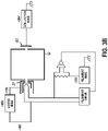
- FIG. 8 Shown in FIG. 8 is a graph illustrating a comparison between collector current and emission current for a dual filament assembly as measured from a ground referenced electron lens power supply when acquired in accordance with FIG. 3A with switch 25 in the upper (ground referenced) position ( a ).
- Such dual filament assemblies are described in US7902529 .
- the X axis represents the setpoint emission current, while the Y axis is the measured collector current.
- the experimental setup of FIG. 3A is emission current regulated but uses a separate collector 40 to determine the emission characteristics of the electron source in emission current regulation mode. As described above, electrons which strike the electron gate lens 31 are counted as emission current when the electron lens bias has a path to earth ground.
- FIG. 9 Shown in FIG. 9 is a graph illustrating a comparison between collector current and emission current for a dual filament supply as measured from a floated electron gating scheme, such as the experimental setup of FIG. 3A with switch 25 moved to the lower (filament referenced) position (b).
- the X axis represents the setpoint emission current, while the Y axis is the measured collector current.
- electrons which strike the electron gate lens 31 are not counted as emission current but are instead returned to the filament supply 38, greatly reducing the "false" emission current registered by the emission measurement system and controls.
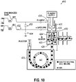
- FIG. 10 shows a mass spectrometer 400 in accordance with an embodiment which includes substantially the same features and functionality as ion trap mass spectrometers 100, 200, except as otherwise described below.
- spectrometer 400 includes a gas chromatograph 423 which provides sample gas to an ion volume 424, and an electron source 430 which provides energetic electrons to the ion source to ionize the atoms and molecules in said device and form positive ions 425 and undesired excited neutrals 426.
- Spectrometer 400 also incorporates an emission current sensing resistor 436 for measuring the current emitted from the filament 431 using the technique described above with reference to FIG. 4 .
- a floated (i.e., a non-ground referenced) capacitor 450 bridging the power supply rails of the filament 431 and electron lens 434 can be included along with resistor 452 to form a floating RC circuit.
- the values of capacitor 450 and resistor 452 are selected to cause the electron lens voltage slew rate to match, or otherwise substantially align with, the filament power supply voltage slew rate.
- An additional, optional capacitor 454 may be provided to the RC circuit, for example, by coupling the output of the power supply for the electron lens 434 to an electrical ground source, to compensate for any instrument-to-instrument differences in the capacitance of electron lens 434 and associated lead wires, board traces etc. Since the capacitance of the electron lens is quite low, this compensation capacitor can be added such that the relative differences in capacitance between instruments are reduced. For example, if one instrument exhibits 10 picofarads of electron lens capacitance to ground while a second instrument exhibits 20 picofarads to ground, the relative difference is 2x.
- the first instrument By selecting a value of 50 picofarads for capacitor 454, the first instrument will exhibit 60 picofarads of capacitance to ground while instrument two exhibits 70 picofarads or a relative difference of 1.17x.
- Typical values for capacitor 450, resistor 452, and capacitor 454 can be, in one example, 1 nano-farad, 5300 ohms, and 50 picofarads, respectively. However, the chosen values for capacity 450, resistor 452, and capacitor 454 may each be varied while still providing the same or a substantially similar functionality as is described herein.
Landscapes
- Chemical & Material Sciences (AREA)
- Analytical Chemistry (AREA)
- Physics & Mathematics (AREA)
- Engineering & Computer Science (AREA)
- Plasma & Fusion (AREA)
- Electron Tubes For Measurement (AREA)
- Other Investigation Or Analysis Of Materials By Electrical Means (AREA)
- Electron Sources, Ion Sources (AREA)
Applications Claiming Priority (2)
| Application Number | Priority Date | Filing Date | Title |
|---|---|---|---|
| US16/721,517 US11145502B2 (en) | 2019-12-19 | 2019-12-19 | Emission current measurement for superior instrument-to-instrument repeatability |
| EP20214479.6A EP3840015B1 (de) | 2019-12-19 | 2020-12-16 | Ionenquellenanordnung mit verbesserter elektronemissionsstrommessung für hervorragende wiederholbarkeit von gerät zu gerät |
Related Parent Applications (2)
| Application Number | Title | Priority Date | Filing Date |
|---|---|---|---|
| EP20214479.6A Division EP3840015B1 (de) | 2019-12-19 | 2020-12-16 | Ionenquellenanordnung mit verbesserter elektronemissionsstrommessung für hervorragende wiederholbarkeit von gerät zu gerät |
| EP20214479.6A Division-Into EP3840015B1 (de) | 2019-12-19 | 2020-12-16 | Ionenquellenanordnung mit verbesserter elektronemissionsstrommessung für hervorragende wiederholbarkeit von gerät zu gerät |
Publications (1)
| Publication Number | Publication Date |
|---|---|
| EP4071784A1 true EP4071784A1 (de) | 2022-10-12 |
Family
ID=73854758
Family Applications (3)
| Application Number | Title | Priority Date | Filing Date |
|---|---|---|---|
| EP20214479.6A Active EP3840015B1 (de) | 2019-12-19 | 2020-12-16 | Ionenquellenanordnung mit verbesserter elektronemissionsstrommessung für hervorragende wiederholbarkeit von gerät zu gerät |
| EP22174694.4A Pending EP4071784A1 (de) | 2019-12-19 | 2020-12-16 | Ionenquelle für gepulsten elektronenionisierungsprozesse |
| EP22174690.2A Withdrawn EP4071783A1 (de) | 2019-12-19 | 2020-12-16 | Ionenquelle für gepulsten elektronenionisierungsprozesse |
Family Applications Before (1)
| Application Number | Title | Priority Date | Filing Date |
|---|---|---|---|
| EP20214479.6A Active EP3840015B1 (de) | 2019-12-19 | 2020-12-16 | Ionenquellenanordnung mit verbesserter elektronemissionsstrommessung für hervorragende wiederholbarkeit von gerät zu gerät |
Family Applications After (1)
| Application Number | Title | Priority Date | Filing Date |
|---|---|---|---|
| EP22174690.2A Withdrawn EP4071783A1 (de) | 2019-12-19 | 2020-12-16 | Ionenquelle für gepulsten elektronenionisierungsprozesse |
Country Status (3)
| Country | Link |
|---|---|
| US (1) | US11145502B2 (de) |
| EP (3) | EP3840015B1 (de) |
| CN (2) | CN114188211B (de) |
Citations (9)
| Publication number | Priority date | Publication date | Assignee | Title |
|---|---|---|---|---|
| US2889461A (en) * | 1953-08-10 | 1959-06-02 | Bendix Aviat Corp | Electron multiplier |
| US4540884A (en) | 1982-12-29 | 1985-09-10 | Finnigan Corporation | Method of mass analyzing a sample by use of a quadrupole ion trap |
| US4736101A (en) | 1985-05-24 | 1988-04-05 | Finnigan Corporation | Method of operating ion trap detector in MS/MS mode |
| US4808820A (en) * | 1987-09-23 | 1989-02-28 | Hewlett-Packard Company | Electron-emission filament cutoff for gas chromatography + mass spectrometry systems |
| US5750993A (en) | 1996-05-09 | 1998-05-12 | Finnigan Corporation | Method of reducing noise in an ion trap mass spectrometer coupled to an atmospheric pressure ionization source |
| US5756996A (en) | 1996-07-05 | 1998-05-26 | Finnigan Corporation | Ion source assembly for an ion trap mass spectrometer and method |
| US6294780B1 (en) * | 1999-04-01 | 2001-09-25 | Varian, Inc. | Pulsed ion source for ion trap mass spectrometer |
| US7323682B2 (en) | 2004-07-02 | 2008-01-29 | Thermo Finnigan Llc | Pulsed ion source for quadrupole mass spectrometer and method |
| US7902529B2 (en) | 2007-08-02 | 2011-03-08 | Thermo Finnigan Llc | Method and apparatus for selectively providing electrons in an ion source |
Family Cites Families (16)
| Publication number | Priority date | Publication date | Assignee | Title |
|---|---|---|---|---|
| GB1131495A (en) | 1965-10-04 | 1968-10-23 | Edwards High Vacuum Int Ltd | Improvements in or relating to electron emission control in mass spectrometers |
| US6177668B1 (en) * | 1996-06-06 | 2001-01-23 | Mds Inc. | Axial ejection in a multipole mass spectrometer |
| JP2006521006A (ja) | 2003-03-03 | 2006-09-14 | ブリガム・ヤング・ユニバーシティ | 直交加速飛行時間型質量分析のための新規な電子イオン化源 |
| WO2005106921A1 (en) * | 2004-05-05 | 2005-11-10 | Mds Inc. Doing Business Through Its Mds Sciex Division | Ion guide for mass spectrometer |
| GB2415541B (en) * | 2004-06-21 | 2009-09-23 | Thermo Finnigan Llc | RF power supply for a mass spectrometer |
| CA2571728A1 (en) * | 2004-07-01 | 2006-02-09 | Ciphergen Biosystems, Inc. | Dynamic biasing of ion optics in a mass spectrometer |
| US7701123B2 (en) | 2005-12-13 | 2010-04-20 | Varian, Inc. | Electron source for ionization with leakage current suppression |
| EP1995763A4 (de) | 2006-03-07 | 2011-09-28 | Shimadzu Corp | Massenanalysator |
| TWI484529B (zh) * | 2006-11-13 | 2015-05-11 | Mks Instr Inc | 離子阱質譜儀、利用其得到質譜之方法、離子阱、捕捉離子阱內之離子之方法和設備 |
| US7622713B2 (en) | 2008-02-05 | 2009-11-24 | Thermo Finnigan Llc | Method and apparatus for normalizing performance of an electron source |
| WO2011125218A1 (ja) * | 2010-04-09 | 2011-10-13 | 株式会社島津製作所 | 四重極型質量分析装置 |
| JP5896775B2 (ja) * | 2012-02-16 | 2016-03-30 | 株式会社ニューフレアテクノロジー | 電子ビーム描画装置および電子ビーム描画方法 |
| CN103367094B (zh) * | 2012-03-31 | 2016-12-14 | 株式会社岛津制作所 | 离子阱分析器以及离子阱质谱分析方法 |
| WO2014164198A1 (en) | 2013-03-11 | 2014-10-09 | David Rafferty | Automatic gain control with defocusing lens |
| US10229822B2 (en) * | 2014-10-20 | 2019-03-12 | Shimadzu Corporation | Mass spectrometer with high-voltage power source |
| JP6508215B2 (ja) | 2014-12-12 | 2019-05-08 | 株式会社島津製作所 | 質量分析装置 |
-
2019
- 2019-12-19 US US16/721,517 patent/US11145502B2/en active Active
-
2020
- 2020-12-16 EP EP20214479.6A patent/EP3840015B1/de active Active
- 2020-12-16 EP EP22174694.4A patent/EP4071784A1/de active Pending
- 2020-12-16 EP EP22174690.2A patent/EP4071783A1/de not_active Withdrawn
- 2020-12-17 CN CN202111521209.9A patent/CN114188211B/zh active Active
- 2020-12-17 CN CN202011498154.XA patent/CN113013015B/zh active Active
Patent Citations (11)
| Publication number | Priority date | Publication date | Assignee | Title |
|---|---|---|---|---|
| US2889461A (en) * | 1953-08-10 | 1959-06-02 | Bendix Aviat Corp | Electron multiplier |
| US4540884A (en) | 1982-12-29 | 1985-09-10 | Finnigan Corporation | Method of mass analyzing a sample by use of a quadrupole ion trap |
| US4736101A (en) | 1985-05-24 | 1988-04-05 | Finnigan Corporation | Method of operating ion trap detector in MS/MS mode |
| US4808820A (en) * | 1987-09-23 | 1989-02-28 | Hewlett-Packard Company | Electron-emission filament cutoff for gas chromatography + mass spectrometry systems |
| US5750993A (en) | 1996-05-09 | 1998-05-12 | Finnigan Corporation | Method of reducing noise in an ion trap mass spectrometer coupled to an atmospheric pressure ionization source |
| US5756996A (en) | 1996-07-05 | 1998-05-26 | Finnigan Corporation | Ion source assembly for an ion trap mass spectrometer and method |
| US6294780B1 (en) * | 1999-04-01 | 2001-09-25 | Varian, Inc. | Pulsed ion source for ion trap mass spectrometer |
| US7323682B2 (en) | 2004-07-02 | 2008-01-29 | Thermo Finnigan Llc | Pulsed ion source for quadrupole mass spectrometer and method |
| US7507954B2 (en) | 2004-07-02 | 2009-03-24 | Thermo Finnigan Llc | Pulsed ion source for quadrupole mass spectrometer method |
| US7759655B2 (en) | 2004-07-02 | 2010-07-20 | Thermo Finnigan Llc | Pulsed ion source for quadrupole mass spectrometer and method |
| US7902529B2 (en) | 2007-08-02 | 2011-03-08 | Thermo Finnigan Llc | Method and apparatus for selectively providing electrons in an ion source |
Also Published As
| Publication number | Publication date |
|---|---|
| US11145502B2 (en) | 2021-10-12 |
| CN113013015A (zh) | 2021-06-22 |
| EP3840015A3 (de) | 2021-09-22 |
| EP3840015B1 (de) | 2023-03-08 |
| CN114188211A (zh) | 2022-03-15 |
| CN114188211B (zh) | 2024-10-22 |
| US20210193449A1 (en) | 2021-06-24 |
| CN113013015B (zh) | 2022-06-03 |
| EP3840015A2 (de) | 2021-06-23 |
| EP4071783A1 (de) | 2022-10-12 |
Similar Documents
| Publication | Publication Date | Title |
|---|---|---|
| US7888635B2 (en) | Ion funnel ion trap and process | |
| US7060987B2 (en) | Electron ionization source for othogonal acceleration time-of-flight mass spectrometry | |
| GB2436004A (en) | Molecular activation of analyte ions in a tandem mass spectrometer | |
| US11764026B2 (en) | Electron source | |
| US4988869A (en) | Method and apparatus for electron-induced dissociation of molecular species | |
| CN110176385A (zh) | 一种用于磁质谱仪的高效离子源 | |
| TWI877257B (zh) | 具有離子源的氣體分析器系統 | |
| EP3840015B1 (de) | Ionenquellenanordnung mit verbesserter elektronemissionsstrommessung für hervorragende wiederholbarkeit von gerät zu gerät | |
| JPH0736326B2 (ja) | イオン・サイクロトロン共鳴のスペクトロメ−タ | |
| US7858933B2 (en) | Mass spectrometer | |
| JP7497779B2 (ja) | 質量分析装置 | |
| JP3750386B2 (ja) | 四重極質量分析装置 | |
| US12009197B2 (en) | Method and apparatus | |
| Mahadevan | Merging beams study of ionization of positive ions by electrons | |
| Prelec et al. | Development of intense negative hydrogen ion sources at BNL |
Legal Events
| Date | Code | Title | Description |
|---|---|---|---|
| PUAI | Public reference made under article 153(3) epc to a published international application that has entered the european phase |
Free format text: ORIGINAL CODE: 0009012 |
|
| STAA | Information on the status of an ep patent application or granted ep patent |
Free format text: STATUS: THE APPLICATION HAS BEEN PUBLISHED |
|
| AC | Divisional application: reference to earlier application |
Ref document number: 3840015 Country of ref document: EP Kind code of ref document: P |
|
| AK | Designated contracting states |
Kind code of ref document: A1 Designated state(s): AL AT BE BG CH CY CZ DE DK EE ES FI FR GB GR HR HU IE IS IT LI LT LU LV MC MK MT NL NO PL PT RO RS SE SI SK SM TR |
|
| STAA | Information on the status of an ep patent application or granted ep patent |
Free format text: STATUS: REQUEST FOR EXAMINATION WAS MADE |
|
| 17P | Request for examination filed |
Effective date: 20230306 |
|
| RBV | Designated contracting states (corrected) |
Designated state(s): AL AT BE BG CH CY CZ DE DK EE ES FI FR GB GR HR HU IE IS IT LI LT LU LV MC MK MT NL NO PL PT RO RS SE SI SK SM TR |
|
| GRAP | Despatch of communication of intention to grant a patent |
Free format text: ORIGINAL CODE: EPIDOSNIGR1 |
|
| STAA | Information on the status of an ep patent application or granted ep patent |
Free format text: STATUS: GRANT OF PATENT IS INTENDED |
|
| INTG | Intention to grant announced |
Effective date: 20260122 |