EP4071127A1 - Copper/ceramic assembly, insulated circuit board, method for producing copper/ceramic assembly, and method for producing insulated circuit board - Google Patents
Copper/ceramic assembly, insulated circuit board, method for producing copper/ceramic assembly, and method for producing insulated circuit board Download PDFInfo
- Publication number
- EP4071127A1 EP4071127A1 EP20896480.9A EP20896480A EP4071127A1 EP 4071127 A1 EP4071127 A1 EP 4071127A1 EP 20896480 A EP20896480 A EP 20896480A EP 4071127 A1 EP4071127 A1 EP 4071127A1
- Authority
- EP
- European Patent Office
- Prior art keywords
- copper
- ceramic
- less
- ceramic substrate
- circuit board
- Prior art date
- Legal status (The legal status is an assumption and is not a legal conclusion. Google has not performed a legal analysis and makes no representation as to the accuracy of the status listed.)
- Pending
Links
Images


Classifications
-
- C—CHEMISTRY; METALLURGY
- C04—CEMENTS; CONCRETE; ARTIFICIAL STONE; CERAMICS; REFRACTORIES
- C04B—LIME, MAGNESIA; SLAG; CEMENTS; COMPOSITIONS THEREOF, e.g. MORTARS, CONCRETE OR LIKE BUILDING MATERIALS; ARTIFICIAL STONE; CERAMICS; REFRACTORIES; TREATMENT OF NATURAL STONE
- C04B37/00—Joining burned ceramic articles with other burned ceramic articles or other articles by heating
- C04B37/02—Joining burned ceramic articles with other burned ceramic articles or other articles by heating with metallic articles
- C04B37/023—Joining burned ceramic articles with other burned ceramic articles or other articles by heating with metallic articles characterised by the interlayer used
- C04B37/026—Joining burned ceramic articles with other burned ceramic articles or other articles by heating with metallic articles characterised by the interlayer used consisting of metals or metal salts
-
- B—PERFORMING OPERATIONS; TRANSPORTING
- B32—LAYERED PRODUCTS
- B32B—LAYERED PRODUCTS, i.e. PRODUCTS BUILT-UP OF STRATA OF FLAT OR NON-FLAT, e.g. CELLULAR OR HONEYCOMB, FORM
- B32B15/00—Layered products comprising a layer of metal
- B32B15/20—Layered products comprising a layer of metal comprising aluminium or copper
-
- B—PERFORMING OPERATIONS; TRANSPORTING
- B32—LAYERED PRODUCTS
- B32B—LAYERED PRODUCTS, i.e. PRODUCTS BUILT-UP OF STRATA OF FLAT OR NON-FLAT, e.g. CELLULAR OR HONEYCOMB, FORM
- B32B37/00—Methods or apparatus for laminating, e.g. by curing or by ultrasonic bonding
- B32B37/14—Methods or apparatus for laminating, e.g. by curing or by ultrasonic bonding characterised by the properties of the layers
- B32B37/16—Methods or apparatus for laminating, e.g. by curing or by ultrasonic bonding characterised by the properties of the layers with all layers existing as coherent layers before laminating
- B32B37/18—Methods or apparatus for laminating, e.g. by curing or by ultrasonic bonding characterised by the properties of the layers with all layers existing as coherent layers before laminating involving the assembly of discrete sheets or panels only
-
- B—PERFORMING OPERATIONS; TRANSPORTING
- B32—LAYERED PRODUCTS
- B32B—LAYERED PRODUCTS, i.e. PRODUCTS BUILT-UP OF STRATA OF FLAT OR NON-FLAT, e.g. CELLULAR OR HONEYCOMB, FORM
- B32B7/00—Layered products characterised by the relation between layers; Layered products characterised by the relative orientation of features between layers, or by the relative values of a measurable parameter between layers, i.e. products comprising layers having different physical, chemical or physicochemical properties; Layered products characterised by the interconnection of layers
- B32B7/04—Interconnection of layers
- B32B7/12—Interconnection of layers using interposed adhesives or interposed materials with bonding properties
-
- B—PERFORMING OPERATIONS; TRANSPORTING
- B32—LAYERED PRODUCTS
- B32B—LAYERED PRODUCTS, i.e. PRODUCTS BUILT-UP OF STRATA OF FLAT OR NON-FLAT, e.g. CELLULAR OR HONEYCOMB, FORM
- B32B9/00—Layered products comprising a layer of a particular substance not covered by groups B32B11/00 - B32B29/00
- B32B9/005—Layered products comprising a layer of a particular substance not covered by groups B32B11/00 - B32B29/00 comprising one layer of ceramic material, e.g. porcelain, ceramic tile
-
- B—PERFORMING OPERATIONS; TRANSPORTING
- B32—LAYERED PRODUCTS
- B32B—LAYERED PRODUCTS, i.e. PRODUCTS BUILT-UP OF STRATA OF FLAT OR NON-FLAT, e.g. CELLULAR OR HONEYCOMB, FORM
- B32B9/00—Layered products comprising a layer of a particular substance not covered by groups B32B11/00 - B32B29/00
- B32B9/04—Layered products comprising a layer of a particular substance not covered by groups B32B11/00 - B32B29/00 comprising such particular substance as the main or only constituent of a layer, which is next to another layer of the same or of a different material
- B32B9/041—Layered products comprising a layer of a particular substance not covered by groups B32B11/00 - B32B29/00 comprising such particular substance as the main or only constituent of a layer, which is next to another layer of the same or of a different material of metal
-
- C—CHEMISTRY; METALLURGY
- C04—CEMENTS; CONCRETE; ARTIFICIAL STONE; CERAMICS; REFRACTORIES
- C04B—LIME, MAGNESIA; SLAG; CEMENTS; COMPOSITIONS THEREOF, e.g. MORTARS, CONCRETE OR LIKE BUILDING MATERIALS; ARTIFICIAL STONE; CERAMICS; REFRACTORIES; TREATMENT OF NATURAL STONE
- C04B35/00—Shaped ceramic products characterised by their composition; Ceramics compositions; Processing powders of inorganic compounds preparatory to the manufacturing of ceramic products
- C04B35/515—Shaped ceramic products characterised by their composition; Ceramics compositions; Processing powders of inorganic compounds preparatory to the manufacturing of ceramic products based on non-oxide ceramics
- C04B35/58—Shaped ceramic products characterised by their composition; Ceramics compositions; Processing powders of inorganic compounds preparatory to the manufacturing of ceramic products based on non-oxide ceramics based on borides, nitrides, i.e. nitrides, oxynitrides, carbonitrides or oxycarbonitrides or silicides
- C04B35/584—Shaped ceramic products characterised by their composition; Ceramics compositions; Processing powders of inorganic compounds preparatory to the manufacturing of ceramic products based on non-oxide ceramics based on borides, nitrides, i.e. nitrides, oxynitrides, carbonitrides or oxycarbonitrides or silicides based on silicon nitride
-
- C—CHEMISTRY; METALLURGY
- C04—CEMENTS; CONCRETE; ARTIFICIAL STONE; CERAMICS; REFRACTORIES
- C04B—LIME, MAGNESIA; SLAG; CEMENTS; COMPOSITIONS THEREOF, e.g. MORTARS, CONCRETE OR LIKE BUILDING MATERIALS; ARTIFICIAL STONE; CERAMICS; REFRACTORIES; TREATMENT OF NATURAL STONE
- C04B35/00—Shaped ceramic products characterised by their composition; Ceramics compositions; Processing powders of inorganic compounds preparatory to the manufacturing of ceramic products
- C04B35/622—Forming processes; Processing powders of inorganic compounds preparatory to the manufacturing of ceramic products
- C04B35/64—Burning or sintering processes
- C04B35/645—Pressure sintering
-
- C—CHEMISTRY; METALLURGY
- C04—CEMENTS; CONCRETE; ARTIFICIAL STONE; CERAMICS; REFRACTORIES
- C04B—LIME, MAGNESIA; SLAG; CEMENTS; COMPOSITIONS THEREOF, e.g. MORTARS, CONCRETE OR LIKE BUILDING MATERIALS; ARTIFICIAL STONE; CERAMICS; REFRACTORIES; TREATMENT OF NATURAL STONE
- C04B37/00—Joining burned ceramic articles with other burned ceramic articles or other articles by heating
- C04B37/02—Joining burned ceramic articles with other burned ceramic articles or other articles by heating with metallic articles
- C04B37/023—Joining burned ceramic articles with other burned ceramic articles or other articles by heating with metallic articles characterised by the interlayer used
-
- H—ELECTRICITY
- H05—ELECTRIC TECHNIQUES NOT OTHERWISE PROVIDED FOR
- H05K—PRINTED CIRCUITS; CASINGS OR CONSTRUCTIONAL DETAILS OF ELECTRIC APPARATUS; MANUFACTURE OF ASSEMBLAGES OF ELECTRICAL COMPONENTS
- H05K1/00—Printed circuits
- H05K1/02—Details
- H05K1/0201—Thermal arrangements, e.g. for cooling, heating or preventing overheating
- H05K1/0203—Cooling of mounted components
-
- H—ELECTRICITY
- H05—ELECTRIC TECHNIQUES NOT OTHERWISE PROVIDED FOR
- H05K—PRINTED CIRCUITS; CASINGS OR CONSTRUCTIONAL DETAILS OF ELECTRIC APPARATUS; MANUFACTURE OF ASSEMBLAGES OF ELECTRICAL COMPONENTS
- H05K1/00—Printed circuits
- H05K1/02—Details
- H05K1/03—Use of materials for the substrate
- H05K1/0306—Inorganic insulating substrates, e.g. ceramic, glass
-
- H—ELECTRICITY
- H05—ELECTRIC TECHNIQUES NOT OTHERWISE PROVIDED FOR
- H05K—PRINTED CIRCUITS; CASINGS OR CONSTRUCTIONAL DETAILS OF ELECTRIC APPARATUS; MANUFACTURE OF ASSEMBLAGES OF ELECTRICAL COMPONENTS
- H05K3/00—Apparatus or processes for manufacturing printed circuits
- H05K3/38—Improvement of the adhesion between the insulating substrate and the metal
-
- H—ELECTRICITY
- H05—ELECTRIC TECHNIQUES NOT OTHERWISE PROVIDED FOR
- H05K—PRINTED CIRCUITS; CASINGS OR CONSTRUCTIONAL DETAILS OF ELECTRIC APPARATUS; MANUFACTURE OF ASSEMBLAGES OF ELECTRICAL COMPONENTS
- H05K3/00—Apparatus or processes for manufacturing printed circuits
- H05K3/38—Improvement of the adhesion between the insulating substrate and the metal
- H05K3/381—Improvement of the adhesion between the insulating substrate and the metal by special treatment of the substrate
-
- H—ELECTRICITY
- H05—ELECTRIC TECHNIQUES NOT OTHERWISE PROVIDED FOR
- H05K—PRINTED CIRCUITS; CASINGS OR CONSTRUCTIONAL DETAILS OF ELECTRIC APPARATUS; MANUFACTURE OF ASSEMBLAGES OF ELECTRICAL COMPONENTS
- H05K3/00—Apparatus or processes for manufacturing printed circuits
- H05K3/38—Improvement of the adhesion between the insulating substrate and the metal
- H05K3/382—Improvement of the adhesion between the insulating substrate and the metal by special treatment of the metal
-
- H—ELECTRICITY
- H05—ELECTRIC TECHNIQUES NOT OTHERWISE PROVIDED FOR
- H05K—PRINTED CIRCUITS; CASINGS OR CONSTRUCTIONAL DETAILS OF ELECTRIC APPARATUS; MANUFACTURE OF ASSEMBLAGES OF ELECTRICAL COMPONENTS
- H05K3/00—Apparatus or processes for manufacturing printed circuits
- H05K3/38—Improvement of the adhesion between the insulating substrate and the metal
- H05K3/388—Improvement of the adhesion between the insulating substrate and the metal by the use of a metallic or inorganic thin film adhesion layer
-
- H—ELECTRICITY
- H10—SEMICONDUCTOR DEVICES; ELECTRIC SOLID-STATE DEVICES NOT OTHERWISE PROVIDED FOR
- H10W—GENERIC PACKAGES, INTERCONNECTIONS, CONNECTORS OR OTHER CONSTRUCTIONAL DETAILS OF DEVICES COVERED BY CLASS H10
- H10W70/00—Package substrates; Interposers; Redistribution layers [RDL]
- H10W70/01—Manufacture or treatment
- H10W70/05—Manufacture or treatment of insulating or insulated package substrates, or of interposers, or of redistribution layers
-
- H—ELECTRICITY
- H10—SEMICONDUCTOR DEVICES; ELECTRIC SOLID-STATE DEVICES NOT OTHERWISE PROVIDED FOR
- H10W—GENERIC PACKAGES, INTERCONNECTIONS, CONNECTORS OR OTHER CONSTRUCTIONAL DETAILS OF DEVICES COVERED BY CLASS H10
- H10W70/00—Package substrates; Interposers; Redistribution layers [RDL]
- H10W70/60—Insulating or insulated package substrates; Interposers; Redistribution layers
- H10W70/67—Insulating or insulated package substrates; Interposers; Redistribution layers characterised by their insulating layers or insulating parts
- H10W70/69—Insulating materials thereof
- H10W70/692—Ceramics or glasses
-
- B—PERFORMING OPERATIONS; TRANSPORTING
- B32—LAYERED PRODUCTS
- B32B—LAYERED PRODUCTS, i.e. PRODUCTS BUILT-UP OF STRATA OF FLAT OR NON-FLAT, e.g. CELLULAR OR HONEYCOMB, FORM
- B32B2250/00—Layers arrangement
- B32B2250/02—2 layers
-
- B—PERFORMING OPERATIONS; TRANSPORTING
- B32—LAYERED PRODUCTS
- B32B—LAYERED PRODUCTS, i.e. PRODUCTS BUILT-UP OF STRATA OF FLAT OR NON-FLAT, e.g. CELLULAR OR HONEYCOMB, FORM
- B32B2255/00—Coating on the layer surface
- B32B2255/20—Inorganic coating
- B32B2255/205—Metallic coating
-
- B—PERFORMING OPERATIONS; TRANSPORTING
- B32—LAYERED PRODUCTS
- B32B—LAYERED PRODUCTS, i.e. PRODUCTS BUILT-UP OF STRATA OF FLAT OR NON-FLAT, e.g. CELLULAR OR HONEYCOMB, FORM
- B32B2311/00—Metals, their alloys or their compounds
-
- B—PERFORMING OPERATIONS; TRANSPORTING
- B32—LAYERED PRODUCTS
- B32B—LAYERED PRODUCTS, i.e. PRODUCTS BUILT-UP OF STRATA OF FLAT OR NON-FLAT, e.g. CELLULAR OR HONEYCOMB, FORM
- B32B2311/00—Metals, their alloys or their compounds
- B32B2311/12—Copper
-
- B—PERFORMING OPERATIONS; TRANSPORTING
- B32—LAYERED PRODUCTS
- B32B—LAYERED PRODUCTS, i.e. PRODUCTS BUILT-UP OF STRATA OF FLAT OR NON-FLAT, e.g. CELLULAR OR HONEYCOMB, FORM
- B32B2315/00—Other materials containing non-metallic inorganic compounds not provided for in groups B32B2311/00 - B32B2313/04
- B32B2315/02—Ceramics
-
- B—PERFORMING OPERATIONS; TRANSPORTING
- B32—LAYERED PRODUCTS
- B32B—LAYERED PRODUCTS, i.e. PRODUCTS BUILT-UP OF STRATA OF FLAT OR NON-FLAT, e.g. CELLULAR OR HONEYCOMB, FORM
- B32B2457/00—Electrical equipment
- B32B2457/08—PCBs, i.e. printed circuit boards
-
- C—CHEMISTRY; METALLURGY
- C04—CEMENTS; CONCRETE; ARTIFICIAL STONE; CERAMICS; REFRACTORIES
- C04B—LIME, MAGNESIA; SLAG; CEMENTS; COMPOSITIONS THEREOF, e.g. MORTARS, CONCRETE OR LIKE BUILDING MATERIALS; ARTIFICIAL STONE; CERAMICS; REFRACTORIES; TREATMENT OF NATURAL STONE
- C04B2235/00—Aspects relating to ceramic starting mixtures or sintered ceramic products
- C04B2235/65—Aspects relating to heat treatments of ceramic bodies such as green ceramics or pre-sintered ceramics, e.g. burning, sintering or melting processes
- C04B2235/656—Aspects relating to heat treatments of ceramic bodies such as green ceramics or pre-sintered ceramics, e.g. burning, sintering or melting processes characterised by specific heating conditions during heat treatment
- C04B2235/6567—Treatment time
-
- C—CHEMISTRY; METALLURGY
- C04—CEMENTS; CONCRETE; ARTIFICIAL STONE; CERAMICS; REFRACTORIES
- C04B—LIME, MAGNESIA; SLAG; CEMENTS; COMPOSITIONS THEREOF, e.g. MORTARS, CONCRETE OR LIKE BUILDING MATERIALS; ARTIFICIAL STONE; CERAMICS; REFRACTORIES; TREATMENT OF NATURAL STONE
- C04B2235/00—Aspects relating to ceramic starting mixtures or sintered ceramic products
- C04B2235/65—Aspects relating to heat treatments of ceramic bodies such as green ceramics or pre-sintered ceramics, e.g. burning, sintering or melting processes
- C04B2235/658—Atmosphere during thermal treatment
- C04B2235/6581—Total pressure below 1 atmosphere, e.g. vacuum
-
- C—CHEMISTRY; METALLURGY
- C04—CEMENTS; CONCRETE; ARTIFICIAL STONE; CERAMICS; REFRACTORIES
- C04B—LIME, MAGNESIA; SLAG; CEMENTS; COMPOSITIONS THEREOF, e.g. MORTARS, CONCRETE OR LIKE BUILDING MATERIALS; ARTIFICIAL STONE; CERAMICS; REFRACTORIES; TREATMENT OF NATURAL STONE
- C04B2235/00—Aspects relating to ceramic starting mixtures or sintered ceramic products
- C04B2235/70—Aspects relating to sintered or melt-casted ceramic products
- C04B2235/80—Phases present in the sintered or melt-cast ceramic products other than the main phase
- C04B2235/85—Intergranular or grain boundary phases
-
- C—CHEMISTRY; METALLURGY
- C04—CEMENTS; CONCRETE; ARTIFICIAL STONE; CERAMICS; REFRACTORIES
- C04B—LIME, MAGNESIA; SLAG; CEMENTS; COMPOSITIONS THEREOF, e.g. MORTARS, CONCRETE OR LIKE BUILDING MATERIALS; ARTIFICIAL STONE; CERAMICS; REFRACTORIES; TREATMENT OF NATURAL STONE
- C04B2237/00—Aspects relating to ceramic laminates or to joining of ceramic articles with other articles by heating
- C04B2237/02—Aspects relating to interlayers, e.g. used to join ceramic articles with other articles by heating
- C04B2237/04—Ceramic interlayers
- C04B2237/08—Non-oxidic interlayers
-
- C—CHEMISTRY; METALLURGY
- C04—CEMENTS; CONCRETE; ARTIFICIAL STONE; CERAMICS; REFRACTORIES
- C04B—LIME, MAGNESIA; SLAG; CEMENTS; COMPOSITIONS THEREOF, e.g. MORTARS, CONCRETE OR LIKE BUILDING MATERIALS; ARTIFICIAL STONE; CERAMICS; REFRACTORIES; TREATMENT OF NATURAL STONE
- C04B2237/00—Aspects relating to ceramic laminates or to joining of ceramic articles with other articles by heating
- C04B2237/02—Aspects relating to interlayers, e.g. used to join ceramic articles with other articles by heating
- C04B2237/04—Ceramic interlayers
- C04B2237/09—Ceramic interlayers wherein the active component for bonding is not the largest fraction of the interlayer
- C04B2237/095—The active component for bonding being silicon
-
- C—CHEMISTRY; METALLURGY
- C04—CEMENTS; CONCRETE; ARTIFICIAL STONE; CERAMICS; REFRACTORIES
- C04B—LIME, MAGNESIA; SLAG; CEMENTS; COMPOSITIONS THEREOF, e.g. MORTARS, CONCRETE OR LIKE BUILDING MATERIALS; ARTIFICIAL STONE; CERAMICS; REFRACTORIES; TREATMENT OF NATURAL STONE
- C04B2237/00—Aspects relating to ceramic laminates or to joining of ceramic articles with other articles by heating
- C04B2237/02—Aspects relating to interlayers, e.g. used to join ceramic articles with other articles by heating
- C04B2237/12—Metallic interlayers
-
- C—CHEMISTRY; METALLURGY
- C04—CEMENTS; CONCRETE; ARTIFICIAL STONE; CERAMICS; REFRACTORIES
- C04B—LIME, MAGNESIA; SLAG; CEMENTS; COMPOSITIONS THEREOF, e.g. MORTARS, CONCRETE OR LIKE BUILDING MATERIALS; ARTIFICIAL STONE; CERAMICS; REFRACTORIES; TREATMENT OF NATURAL STONE
- C04B2237/00—Aspects relating to ceramic laminates or to joining of ceramic articles with other articles by heating
- C04B2237/30—Composition of layers of ceramic laminates or of ceramic or metallic articles to be joined by heating, e.g. Si substrates
- C04B2237/32—Ceramic
- C04B2237/36—Non-oxidic
- C04B2237/368—Silicon nitride
-
- C—CHEMISTRY; METALLURGY
- C04—CEMENTS; CONCRETE; ARTIFICIAL STONE; CERAMICS; REFRACTORIES
- C04B—LIME, MAGNESIA; SLAG; CEMENTS; COMPOSITIONS THEREOF, e.g. MORTARS, CONCRETE OR LIKE BUILDING MATERIALS; ARTIFICIAL STONE; CERAMICS; REFRACTORIES; TREATMENT OF NATURAL STONE
- C04B2237/00—Aspects relating to ceramic laminates or to joining of ceramic articles with other articles by heating
- C04B2237/30—Composition of layers of ceramic laminates or of ceramic or metallic articles to be joined by heating, e.g. Si substrates
- C04B2237/40—Metallic
- C04B2237/407—Copper
-
- C—CHEMISTRY; METALLURGY
- C04—CEMENTS; CONCRETE; ARTIFICIAL STONE; CERAMICS; REFRACTORIES
- C04B—LIME, MAGNESIA; SLAG; CEMENTS; COMPOSITIONS THEREOF, e.g. MORTARS, CONCRETE OR LIKE BUILDING MATERIALS; ARTIFICIAL STONE; CERAMICS; REFRACTORIES; TREATMENT OF NATURAL STONE
- C04B2237/00—Aspects relating to ceramic laminates or to joining of ceramic articles with other articles by heating
- C04B2237/50—Processing aspects relating to ceramic laminates or to the joining of ceramic articles with other articles by heating
- C04B2237/59—Aspects relating to the structure of the interlayer
- C04B2237/592—Aspects relating to the structure of the interlayer whereby the interlayer is not continuous, e.g. not the whole surface of the smallest substrate is covered by the interlayer
-
- C—CHEMISTRY; METALLURGY
- C04—CEMENTS; CONCRETE; ARTIFICIAL STONE; CERAMICS; REFRACTORIES
- C04B—LIME, MAGNESIA; SLAG; CEMENTS; COMPOSITIONS THEREOF, e.g. MORTARS, CONCRETE OR LIKE BUILDING MATERIALS; ARTIFICIAL STONE; CERAMICS; REFRACTORIES; TREATMENT OF NATURAL STONE
- C04B2237/00—Aspects relating to ceramic laminates or to joining of ceramic articles with other articles by heating
- C04B2237/50—Processing aspects relating to ceramic laminates or to the joining of ceramic articles with other articles by heating
- C04B2237/60—Forming at the joining interface or in the joining layer specific reaction phases or zones, e.g. diffusion of reactive species from the interlayer to the substrate or from a substrate to the joining interface, carbide forming at the joining interface
-
- H—ELECTRICITY
- H05—ELECTRIC TECHNIQUES NOT OTHERWISE PROVIDED FOR
- H05K—PRINTED CIRCUITS; CASINGS OR CONSTRUCTIONAL DETAILS OF ELECTRIC APPARATUS; MANUFACTURE OF ASSEMBLAGES OF ELECTRICAL COMPONENTS
- H05K2201/00—Indexing scheme relating to printed circuits covered by H05K1/00
- H05K2201/06—Thermal details
- H05K2201/066—Heatsink mounted on the surface of the printed circuit board [PCB]
-
- H—ELECTRICITY
- H05—ELECTRIC TECHNIQUES NOT OTHERWISE PROVIDED FOR
- H05K—PRINTED CIRCUITS; CASINGS OR CONSTRUCTIONAL DETAILS OF ELECTRIC APPARATUS; MANUFACTURE OF ASSEMBLAGES OF ELECTRICAL COMPONENTS
- H05K2203/00—Indexing scheme relating to apparatus or processes for manufacturing printed circuits covered by H05K3/00
- H05K2203/06—Lamination
-
- H—ELECTRICITY
- H10—SEMICONDUCTOR DEVICES; ELECTRIC SOLID-STATE DEVICES NOT OTHERWISE PROVIDED FOR
- H10W—GENERIC PACKAGES, INTERCONNECTIONS, CONNECTORS OR OTHER CONSTRUCTIONAL DETAILS OF DEVICES COVERED BY CLASS H10
- H10W40/00—Arrangements for thermal protection or thermal control
- H10W40/20—Arrangements for cooling
- H10W40/25—Arrangements for cooling characterised by their materials
- H10W40/255—Arrangements for cooling characterised by their materials having a laminate or multilayered structure, e.g. direct bond copper [DBC] ceramic substrates
-
- H—ELECTRICITY
- H10—SEMICONDUCTOR DEVICES; ELECTRIC SOLID-STATE DEVICES NOT OTHERWISE PROVIDED FOR
- H10W—GENERIC PACKAGES, INTERCONNECTIONS, CONNECTORS OR OTHER CONSTRUCTIONAL DETAILS OF DEVICES COVERED BY CLASS H10
- H10W40/00—Arrangements for thermal protection or thermal control
- H10W40/40—Arrangements for thermal protection or thermal control involving heat exchange by flowing fluids
-
- H—ELECTRICITY
- H10—SEMICONDUCTOR DEVICES; ELECTRIC SOLID-STATE DEVICES NOT OTHERWISE PROVIDED FOR
- H10W—GENERIC PACKAGES, INTERCONNECTIONS, CONNECTORS OR OTHER CONSTRUCTIONAL DETAILS OF DEVICES COVERED BY CLASS H10
- H10W40/00—Arrangements for thermal protection or thermal control
- H10W40/40—Arrangements for thermal protection or thermal control involving heat exchange by flowing fluids
- H10W40/47—Arrangements for thermal protection or thermal control involving heat exchange by flowing fluids by flowing liquids, e.g. forced water cooling
-
- H—ELECTRICITY
- H10—SEMICONDUCTOR DEVICES; ELECTRIC SOLID-STATE DEVICES NOT OTHERWISE PROVIDED FOR
- H10W—GENERIC PACKAGES, INTERCONNECTIONS, CONNECTORS OR OTHER CONSTRUCTIONAL DETAILS OF DEVICES COVERED BY CLASS H10
- H10W72/00—Interconnections or connectors in packages
- H10W72/30—Die-attach connectors
- H10W72/351—Materials of die-attach connectors
- H10W72/352—Materials of die-attach connectors comprising metals or metalloids, e.g. solders
-
- H—ELECTRICITY
- H10—SEMICONDUCTOR DEVICES; ELECTRIC SOLID-STATE DEVICES NOT OTHERWISE PROVIDED FOR
- H10W—GENERIC PACKAGES, INTERCONNECTIONS, CONNECTORS OR OTHER CONSTRUCTIONAL DETAILS OF DEVICES COVERED BY CLASS H10
- H10W90/00—Package configurations
- H10W90/701—Package configurations characterised by the relative positions of pads or connectors relative to package parts
- H10W90/731—Package configurations characterised by the relative positions of pads or connectors relative to package parts of die-attach connectors
- H10W90/734—Package configurations characterised by the relative positions of pads or connectors relative to package parts of die-attach connectors between a chip and a stacked insulating package substrate, interposer or RDL
Definitions
- the present invention relates to a copper-ceramic bonded body in which a copper member made of copper or a copper alloy and a ceramic member made of silicon nitride are bonded to each other, an insulated circuit board in which a copper sheet made of copper or a copper alloy is bonded to a surface of a ceramic substrate, a method for producing a copper-ceramic bonded body, and a method for producing an insulated circuit board.
- a power module, an LED module, and a thermoelectric module have a structure in which a power semiconductor element, an LED element, and a thermoelectric element are bonded to an insulated circuit board in which a circuit layer made of a conductive material is formed on one surface of an insulating layer.
- a power semiconductor element for high-power control used for controlling a wind power generation, an electric vehicle, a hybrid vehicle, or the like has a large amount of heat generated during operation. Therefore, as a substrate on which the power semiconductor element is mounted, an insulated circuit board including a ceramic substrate and a circuit layer formed by bonding a metal plate having excellent conductivity to one surface of the ceramic substrate has been widely used in the related art. As the insulated circuit board, one having a metal layer formed by bonding a metal plate to the other surface of the ceramic substrate is also provided.
- Patent Document 1 proposes an insulated circuit board in which a circuit layer and a metal layer are formed by bonding a copper sheet to one surface and the other surface of a ceramic substrate.
- the copper sheet is disposed on one surface and the other surface of the ceramic substrate with an Ag-Cu-Ti-based brazing material interposed therebetween, and the copper sheet is bonded thereto by performing a heating treatment (so-called active metal brazing method).
- active metal brazing method since the brazing material containing Ti as an active metal is used, the wettability between the molten brazing material and the ceramic substrate is improved, and the ceramic substrate and the copper sheet are satisfactorily bonded to each other.
- Patent Document 2 proposes an insulated circuit board in which a ceramic substrate and a copper sheet are bonded to each other by using a Cu-Mg-Ti-based brazing material.
- Patent Document 2 a configuration in which bonding is achieved by heating at 560°C to 800°C in a nitrogen gas atmosphere is provided, and Mg in a Cu-Mg-Ti alloy sublimates and does not remain at a bonded interface, while titanium nitride (TiN) is not substantially formed.
- the insulated circuit board tends to be loaded with a large current and a high voltage. Therefore, in the insulated circuit board, it is required to improve the insulating property of the ceramic substrate.
- the invention has been made in view of the above-described circumstances, and an objective thereof is to provide a copper-ceramic bonded body, an insulated circuit board, a method for producing a copper-ceramic bonded body, and a method for an insulated circuit board, which are excellent in insulating properties.
- a copper-ceramic bonded body includes a copper member made of copper or a copper alloy, and a ceramic member made of silicon nitride, the copper member and the ceramic member being bonded to each other, in which a maximum length of a Mg-N compound phase which is present at a bonded interface between the copper member and the ceramic member is less than 100 nm, and in a unit length along the bonded interface, the number density of the Mg-N compound phase in a range of a length of 10 nm or more and less than 100 nm is less than 8 pieces/ ⁇ m.
- the maximum length of the Mg-N compound phase which is present at the bonded interface between the copper member and the ceramic member is less than 100 nm, and in the unit length along the bonded interface, the number density of the Mg-N compound phase in the range of the length of 10 nm or more and less than 100 nm is less than 8 pieces/ ⁇ m, occurrence of electric field concentration caused by the Mg-N compound phase which is present at the bonded interface can be suppressed. Accordingly, the insulating property of the copper-ceramic bonded body can be sufficiently improved.
- the ceramic member includes silicon nitride phases and a glass phase formed between the silicon nitride phases, and Cu atoms are present inside the glass phase located on a side of the copper member.
- the ceramic member includes the silicon nitride phases and the glass phase formed between the silicon nitride phases, and the Cu atoms are present inside the glass phase located on the copper member side, an interfacial reaction between the ceramic member and the copper member is sufficiently performed, and bonding reliability is particularly excellent.
- the total amount of Mg, N, and Si in the Mg-N compound phase is 100 atomic%, a Si concentration is 25 atomic% or less.
- the Si concentration in the Mg-N compound phase is 25 atomic% or less, local precipitation of a Si single phase inside the Mg-N compound phase can be suppressed, and the strength of the Mg-N compound phase can be sufficiently secured. Thereby, it is possible to suppress cracks in the Mg-N compound phase when a load is applied to the bonded interface by ultrasonic bonding of a terminal material, and to maintain an anchor effect by the Mg-N compound phase.
- An insulated circuit board includes a copper sheet made of copper or a copper alloy, and a ceramic substrate made of silicon nitride, the copper sheet being bonded to a surface of the ceramic substrate, in which a maximum length of a Mg-N compound phase which is present at a bonded interface between the copper sheet and the ceramic substrate is less than 100 nm, and in a unit length along the bonded interface, the number density of the Mg-N compound phase in a range of a length of 10 nm or more and less than 100 nm is less than 8 pieces/ ⁇ m.
- the insulated circuit board according to the present invention since the maximum length of the Mg-N compound phase which is present at the bonded interface between the copper sheet and the ceramic substrate is less than 100 nm, and in the unit length along the bonded interface, the number density of the Mg-N compound phase in the range of the length of 10 nm or more and less than 100 nm is less than 8 pieces/ ⁇ m, occurrence of electric field concentration caused by the Mg-N compound phase which is present at the bonded interface can be suppressed. Accordingly, the insulating property of the insulated circuit board can be sufficiently improved.
- the ceramic substrate includes silicon nitride phases and a glass phase formed between the silicon nitride phases, and that Cu atoms are present inside the glass phase located on a side of the copper sheet.
- the ceramic substrate includes the silicon nitride phases and the glass phase formed between the silicon nitride phases, and the Cu atoms are present inside the glass phase located on the copper sheet side, an interfacial reaction between the ceramic substrate and the copper sheet is sufficiently performed, and the bonding reliability is particularly excellent.
- the insulated circuit board according to the present invention it is preferable that assuming that the total amount of Mg, N, and Si in the Mg-N compound phase is 100 atomic%, and the Si concentration is 25 atomic% or less.
- the Si concentration in the Mg-N compound phase is 25 atomic% or less, local precipitation of a Si single phase inside the Mg-N compound phase can be suppressed, and the strength of the Mg-N compound phase can be sufficiently secured. Thereby, it is possible to suppress cracks in the Mg-N compound phase when a load is applied to the bonded interface by ultrasonic bonding of a terminal material, and to maintain an anchor effect by the Mg-N compound phase.
- a method for producing a copper-ceramic bonded body according to the present invention is a method for producing the copper-ceramic bonded body described above, the method including a Mg-disposing step of disposing Mg between the copper member and the ceramic member, a laminating step of laminating the copper member and the ceramic member with Mg interposed therebetween, and a bonding step of performing a heating treatment on the laminated copper member and ceramic member with Mg interposed therebetween in a state of being pressed in a lamination direction under a vacuum atmosphere to bond the copper member and the ceramic member to each other, in which, in the Mg-disposing step, an amount of Mg is in a range of 0.34 mg/cm 2 or more and 2.09 mg/cm 2 or less, and in the bonding step, a temperature integration value obtained from a value of multiplying a temperature and a time at a Mg-Si eutectic temperature (639°C) or higher is in a range of 40 °C ⁇ h
- the amount of Mg is 0.34 mg/cm 2 or more
- the temperature integration value obtained from a value of multiplying a temperature and a time at the Mg-Si eutectic temperature (639°C) or higher is 40 °C ⁇ h or higher, so that a Cu-Mg liquid phase necessary for the interfacial reaction can be sufficiently obtained, and the copper member and the ceramic member can be reliably bonded to each other. Accordingly, the bonding reliability can be improved.
- the amount of Mg is 2.09 mg/cm 2 or less
- the temperature integration value obtained from a value of multiplying a temperature and a time at the Mg-Si eutectic temperature (639°C) or higher is 420 °C ⁇ h or lower, so that excessive formation and growth of the Mg-N compound phase at the bonded interface between the copper member and the ceramic member can be suppressed. Accordingly, the insulating property can be improved.
- a method for producing an insulated circuit board according to the present invention is a method for producing the insulated circuit board described above, the method including a Mg-disposing step of disposing Mg between the copper sheet and the ceramic substrate, a laminating step of laminating the copper sheet and the ceramic substrate with Mg interposed therebetween, and a bonding step of performing a heating treatment on the laminated copper sheet and ceramic substrate with Mg interposed therebetween in a state of being pressed in a lamination direction under a vacuum atmosphere to bond the copper sheet and the ceramic substrate to each other, in which, in the Mg-disposing step, an amount of Mg is in a range of 0.34 mg/cm 2 or more and 2.09 mg/cm 2 or less, and in the bonding step, a temperature integration value obtained from a value of multiplying a temperature and a time at a Mg-Si eutectic temperature (639°C) or higher is in a range of 40 °C ⁇ h or higher and 420 °C ⁇
- the amount of Mg is 0.34 mg/cm 2 or more
- the temperature integration value obtained from a value of multiplying a temperature and a time at the Mg-Si eutectic temperature (639°C) or higher is 40 °C ⁇ h or higher, so that a Cu-Mg liquid phase necessary for the interfacial reaction can be sufficiently obtained, and the copper sheet and the ceramic substrate can be reliably bonded to each other. Accordingly, the bonding reliability can be improved.
- the amount of Mg is 2.09 mg/cm 2 or less
- the temperature integration value obtained from a value of multiplying a temperature and a time at the Mg-Si eutectic temperature (639°C) or higher is 420 °C ⁇ h or lower, so that excessive formation and growth of the Mg-N compound phase at the bonded interface between the copper sheet and the ceramic substrate can be suppressed. Accordingly, the insulating property can be improved.
- a copper-ceramic bonded body an insulated circuit board, a method for producing a copper-ceramic bonded body, and a method for producing an insulated circuit board, which are excellent in insulating properties.
- a copper-ceramic bonded body according to the present embodiment is an insulated circuit board 10 formed by bonding a ceramic substrate 11 as a ceramic member made of ceramics to a copper sheet 22 (circuit layer 12) and a copper sheet 23 (metal layer 13) as a copper member made of copper or a copper alloy.
- Fig. 1 shows a power module 1 including the insulated circuit board 10 according to the present embodiment.
- the power module 1 includes the insulated circuit board 10 on which the circuit layer 12 and the metal layer 13 are disposed, a semiconductor element 3 bonded to one surface (upper surface in Fig. 1 ) of the circuit layer 12 with a bonding layer 2 interposed therebetween, and a heat sink 30 disposed on the other side (lower side in Fig. 1 ) of the metal layer 13.
- the semiconductor element 3 is made of a semiconductor material such as Si.
- the semiconductor element 3 and the circuit layer 12 are bonded to each other with the bonding layer 2 interposed therebetween.
- the bonding layer 2 is made of, for example, a Sn-Ag-based, Sn-In-based, or Sn-Ag-Cu-based solder material.
- the heat sink 30 dissipates heat from the insulated circuit board 10 described above.
- the heat sink 30 is made of Cu or a Cu alloy, and in the present embodiment, the heat sink 30 is made of phosphorus deoxidized copper.
- the heat sink 30 is provided with a passage 31 through which a cooling fluid flows.
- the heat sink 30 and the metal layer 13 are bonded to each other by a solder layer 32 made of a solder material.
- the solder layer 32 is made of, for example, a Sn-Ag-based, Sn-In-based, or Sn-Ag-Cu-based solder material.
- the insulated circuit board 10 of the present embodiment includes the ceramic substrate 11, the circuit layer 12 disposed on one surface (upper surface in Fig. 1 ) of the ceramic substrate 11, and the metal layer 13 disposed on the other surface (lower surface in Fig. 1 ) of the ceramic substrate 11.
- the ceramic substrate 11 is made of silicon nitride (Si 3 N 4 ) having excellent insulating property and heat radiation.
- the thickness of the ceramic substrate 11 is set to be in a range of, for example, 0.2 mm or more and 1.5 mm or less, and in the present embodiment, the thickness is set to 0.32 mm.
- the circuit layer 12 is formed by bonding the copper sheet 22 made of copper or a copper alloy to one surface (upper surface in Fig. 5 ) of the ceramic substrate 11.
- the circuit layer 12 is formed by bonding the copper sheet 22 made of a rolled plate of oxygen-free copper to the ceramic substrate 11.
- the thickness of the copper sheet 22 serving as the circuit layer 12 is set to be in a range of 0.1 mm or more and 2.0 mm or less, and in the present embodiment, the thickness is set to 0.6 mm.
- the metal layer 13 is formed by bonding the copper sheet 23 made of copper or a copper alloy to the other surface (lower surface in Fig. 5 ) of the ceramic substrate 11.
- the metal layer 13 is formed by bonding the copper sheet 23 made of a rolled plate of oxygen-free copper to the ceramic substrate 11.
- the thickness of the copper sheet 23 serving as the metal layer 13 is set to be in a range of 0.1 mm or more and 2.0 mm or less, and in the present embodiment, the thickness is set to 0.6 mm.
- a Mg-N compound phase extending from a side of the ceramic substrate 11 to a side of the circuit layer 12 (metal layer 13) may be formed.
- the Mg-N compound phase is formed by reacting magnesium (Mg) used as a bonding material with nitrogen (N) contained in the ceramic substrate 11.
- the maximum length of a Mg-N compound phase 15 which is present at the bonded interface S between the ceramic substrate 11 and the circuit layer 12 (metal layer 13) is less than 100 nm, and in a unit length along the bonded interface S, the number density of the Mg-N compound phase 15 in a range of a length of 10 nm or more and less than 100 nm is less than 8 pieces/ ⁇ m.
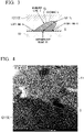
- the dotted line in Fig. 4 is the length along the bonded interface S.
- contact points of the Mg-N compound phase 15 and the bonded interface S are defined as a left end A and a right end B, a point located in a half of the length along the bonded interface S from the left end A to the right end B is defined as an intermediate point PI, a boundary between the Mg-N compound phase 15 and the circuit layer 12 (metal layer 13) is defined as a boundary line C, and an inflection point of the boundary line C is defined as a tip P2.
- a distance L between the intermediate point P1 and the tip P2 is defined as the length.
- the number density of the Mg-N compound phase 15 in a range of a length of 10 nm or more and less than 100 nm is preferably less than 5 pieces/ ⁇ m, and more preferably less than 3 pieces/ ⁇ m.
- the lower limit of the number density of the Mg-N compound phase 15 in the range of the length of 10 nm or more and less than 100 nm may be 0 pieces/ ⁇ m.
- the maximum length of the Mg-N compound phase 15 is preferably 10 nm or more.
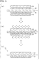
- Fig. 4 shows observation results in the vicinity of the bonded interface S between the ceramic substrate 11 and the circuit layer 12 (metal layer 13).
- Fig. 4 is a STEM-HAADF image obtained by observing the cross section along the lamination direction of the ceramic substrate 11 and the circuit layer 12 (metal layer 13) using a Titan ChemiSTEM manufactured by FEI Company.
- the ceramic substrate 11 includes silicon nitride phases 11a and a glass phase 11b formed between the silicon nitride phases 11a, and that Cu atoms are present inside the glass phase 11b located on a side of the circuit layer 12 (metal layer 13).
- the glass phase 11b is formed by a sintering aid used when sintering a raw material of silicon nitride, and is present at a grain boundary portion between the silicon nitride phases 11a.
- the insulated circuit board 10 it is preferable that assuming that the total amount of Mg, N, and Si in the Mg-N compound phase 15 is 100 atomic%, a Si concentration is 25 atomic% or less.
- a Si concentration in the Mg-N compound phase 15 is 25 atomic% or less, local precipitation of a Si single phase inside the Mg-N compound phase 15 can be suppressed, and the strength of the Mg-N compound phase 15 can be sufficiently secured. Thereby, it is possible to suppress cracks in the Mg-N compound phase 15 when a load is applied to the bonded interface by ultrasonic bonding of a terminal material, and to maintain an anchor effect by the Mg-N compound phase 15.
- the Si concentration is more preferably 20 atomic% or less, and the lower limit thereof is 5 atomic%.
- the ceramic substrate 11 made of silicon nitride (Si 3 N 4 ) is prepared, and as shown in (a) of Fig. 6 , Mg is disposed between the copper sheet 22 serving as the circuit layer 12 and the ceramic substrate 11, and between the copper sheet 23 serving as the metal layer 13 and the ceramic substrate 11.
- a Mg foil 25 is disposed between the copper sheet 22 serving as the circuit layer 12 and the ceramic substrate 11, and between the copper sheet 23 serving as the metal layer 13 and the ceramic substrate 11.
- the amount of Mg to be disposed is in a range of 0.34 mg/cm 2 or more and 2.09 mg/cm 2 or less.
- the amount of Mg to be disposed By setting the amount of Mg to be disposed to 0.34 mg/cm 2 or more, a Cu-Mg liquid phase necessary for the interfacial reaction can be sufficiently obtained, and the copper sheet and the ceramic substrate can be reliably bonded to each other. On the other hand, by limiting the amount of Mg to be disposed to 2.09 mg/cm 2 or less, the excessive formation and growth of the Mg-N compound phase can be suppressed.
- the lower limit of the amount of Mg to be disposed is preferably 0.43 mg/cm 2 or more, and more preferably 0.52 mg/cm 2 or more.
- the upper limit of the amount of Mg to be disposed is preferably 1.34 mg/cm 2 or less, and more preferably 1.04 mg/cm 2 or less.
- the copper sheet 22 and the ceramic substrate 11 are laminated with the Mg foil 25 interposed therebetween, and the ceramic substrate 11 and the copper sheet 23 are laminated with the Mg foil 25 interposed therebetween.
- the copper sheet 22, the Mg foil 25, the ceramic substrate 11, the Mg foil 25, and the copper sheet 23, which are laminated, are pressed in the lamination direction, and are loaded into a vacuum furnace and heated such that the copper sheet 22, the ceramic substrate 11, and the copper sheet 23 are bonded together.
- the temperature rising rate, the holding temperature, the holding time, and the temperature dropping rate are set such that the temperature integration value obtained from a value of multiplying the temperature and the time at the Mg-Si eutectic temperature (639°C) or higher is set to be in a range of 40 °C ⁇ h or higher and 420 °C ⁇ h or lower.
- the temperature integration value obtained from the value of multiplying the temperature and the time at the Mg-Si eutectic temperature (639°C) or higher is set to 40 °C ⁇ h or higher, the Cu-Mg liquid phase necessary for the interfacial reaction can be sufficiently obtained, and the copper sheet and the ceramic substrate can be reliably bonded to each other.
- the above-described temperature integration value is set to 420 °C ⁇ h or lower, the excessive formation and growth of the Mg-N compound phase can be suppressed.
- the lower limit of the temperature integration value obtained from the value of multiplying the temperature and the time at the Mg-Si eutectic temperature (639°C) or higher is preferably 100 °C ⁇ h or higher, and more preferably 150 °C ⁇ h or higher.
- the upper limit of the temperature integration value obtained from the value of multiplying the temperature and the time at the Mg-Si eutectic temperature (639°C) or higher is preferably 400 °C ⁇ h or lower, more preferably 350 °C ⁇ h or lower, and still more preferably 300 °C ⁇ h or lower.
- a pressing load in the bonding step S03 is preferably in a range of 0.049 MPa or more and 3.4 MPa or less.
- a degree of vacuum in the bonding step S03 is preferably in a range of 1 ⁇ 10 -6 Pa or more and 5 ⁇ 10 -2 Pa or less.
- the insulated circuit board 10 according to the present embodiment shown in (c) of Fig. 6 is produced by the Mg-disposing step S01, the laminating step S02, and the bonding step S03.
- the heat sink 30 is bonded to the other surface side of the metal layer 13 of the insulated circuit board 10.
- the insulated circuit board 10 and the heat sink 30 are laminated with a solder material interposed therebetween and are loaded into a heating furnace such that the insulated circuit board 10 and the heat sink 30 are solder-bonded to each other with the solder layer 32 interposed therebetween.
- the semiconductor element 3 is bonded to one surface of the circuit layer 12 of the insulated circuit board 10 by soldering.
- the power module 1 shown in Fig. 1 is produced by the above steps.
- the insulated circuit board 10 (copper-ceramic bonded body) according to the present embodiment having the above configuration, since the maximum length of the Mg-N compound phase 15 which is present at the bonded interface between the circuit layer 12 (and the metal layer 13) and the ceramic substrate 11 is less than 100 nm, and in the unit length along the bonded interface, the number density of the Mg-N compound phase 15 in the range of the length of 10 nm or more and less than 100 nm is less than 8 pieces/ ⁇ m, occurrence of electric field concentration caused by the Mg-N compound phase 15 which is present at the bonded interface can be suppressed. Accordingly, the insulating property of the insulated circuit board 10 can be sufficiently improved.
- the ceramic substrate 11 includes the silicon nitride phases 11a and the glass phase 11b formed between the silicon nitride phases 11a, and Cu atoms are present inside the glass phase 11b located on the circuit layer 12 (and the metal layer 13) side, an interfacial reaction between the ceramic substrate 11 and the copper sheets 22 and 23 is sufficiently performed, and bonding reliability between the circuit layer 12 (and the metal layer 13) and the ceramic substrate 11 is particularly excellent.
- the Si concentration is 25 atomic% or less. In this case, local precipitation of a Si single phase inside the Mg-N compound phase 15 can be suppressed, and the strength of the Mg-N compound phase 15 can be sufficiently secured.
- the amount of Mg is 0.34 mg/cm 2 or more
- the temperature integration value obtained from the value of multiplying a temperature and a time at the Mg-Si eutectic temperature (639°C) or higher is 40 °C ⁇ h or higher, so that a Cu-Mg liquid phase necessary for the interfacial reaction can be sufficiently obtained, and the copper sheets 22 and 23 and the ceramic substrate 11 can be reliably bonded to each other.
- the amount of Mg is 2.09 mg/cm 2 or less
- the temperature integration value obtained from the value of multiplying a temperature and a time at the Mg-Si eutectic temperature (639°C) or higher is 420 °C ⁇ h or lower, so that excessive formation and growth of the Mg-N compound phase at the bonded interface between the circuit layer 12 (and the metal layer 13) and the ceramic substrate 11 can be suppressed.
- the semiconductor element is mounted on the insulated circuit board to form the power module, but the present embodiment is not limited thereto.
- an LED element may be mounted on the circuit layer of the insulated circuit board to form an LED module
- a thermoelectric element may be mounted on the circuit layer of the insulated circuit board to form a thermoelectric module.
- the circuit layer and the metal layer are both made of a copper sheet made of copper or a copper alloy, but the present invention is not limited thereto.
- the circuit layer and the ceramic substrate are made of the copper-ceramic bonded body according to the present invention
- the material and the bonding method of the metal layer there is no limitation on the material and the bonding method of the metal layer.
- the metal layer may be made of aluminum or an aluminum alloy, or may be made of a laminate of copper and aluminum.
- the metal layer and the ceramic substrate are made of the copper-ceramic bonded body according to the present invention
- the material and the bonding method of the circuit layer there is no limitation on the material and the bonding method of the circuit layer.
- the circuit layer may be made of aluminum or an aluminum alloy, or may be made of a laminate of copper and aluminum.
- the Mg foil is laminated between the copper sheet and the ceramic substrate in the Mg-disposing step, but the present invention is not limited thereto, and a thin film made of Mg may be formed on the bonding surface of the ceramic substrate and the copper sheet by a sputtering method, a vapor deposition method, or the like.
- a paste using Mg or MgH 2 may be applied.
- a ceramic substrate (40 mm ⁇ 40 mm ⁇ 0.32 mm) made of a ceramic substrate made of silicon nitride (Si 3 N 4 ) was prepared.
- a copper sheet (37 mm ⁇ 37 mm ⁇ thickness of 0.6 mm) made of oxygen-free copper was bonded to both surfaces of the ceramic substrate under the conditions of the Mg-disposing step and the bonding step shown in Table 1 to obtain an insulated circuit board (copper-ceramic bonded body).
- the degree of vacuum of a vacuum furnace at the time of bonding was set to 2 ⁇ 10 -3 Pa.
- the maximum length of the Mg-N compound phase at the bonded interface the number density of the Mg-N compound phase in the range of the length of 10 nm or more and less than 100 nm, the presence or absence of Cu atoms inside the glass phase, the bonding rate after a thermal cycle, and the dielectric breakdown voltage were evaluated as follows.
- the bonded interface between the copper sheet and the ceramic substrate was observed using a transmission electron microscope (Titan ChemiSTEM manufactured by FEI Company) at an acceleration voltage of 200 kV and a magnification of 20,000x, and the Mg-N compound phase was recognized when a region where Mg and N coexisted was present and the concentration of Mg was 40 atomic% or more and 65 atomic% or less with the total of Mg, N, and Si being 100 atomic% in the region.
- a transmission electron microscope Tian ChemiSTEM manufactured by FEI Company
- the maximum length of the Mg-N compound phase and the number density of the Mg-N compound phase in the range of the length of 10 nm or more and less than 100 nm in the unit length along the bonded interface were calculated.
- the maximum length of the Mg-N compound phase was measured by extracting, in the cross section of the copper-ceramic bonded body, the Mg-N compound phase in the field of view (2 ⁇ m ⁇ 2 ⁇ m) when the bonded interface was observed using a transmission electron microscope (Titan ChemiSTEM manufactured by FE1 Company), and by measuring the length of the Mg-N compound phase according to the above definition. The measurement was performed in 5 fields of view in each copper-ceramic bonded body, and the length of the Mg-N compound phase, which had the largest length, was shown as the maximum length of the Mg-N compound phase.
- the number density (pieces/ ⁇ m) of the Mg-N compound phase was calculated by counting the number of the Mg-N compound phases in the range of the length of 10 nm or more and less than 100 nm in the unit length along the bonded interface between the copper sheet and the ceramic substrate in the field of view (2 ⁇ m ⁇ 2 ⁇ m) when the cross section of the copper-ceramic bonded body cut along the lamination direction of the copper-ceramic bonded body was observed using a transmission electron microscope (Titan ChemiSTEM manufactured by FEI Company). The measurement was performed in 5 fields of view, and an average value was shown as the number density (pieces/ ⁇ m).
- the evaluation results are shown in Table 1.
- the maximum length of the Mg-N compound phase and the number density of the Mg-N compound phase were measured by excluding the Mg-N compound phase which was present at the boundary of the measurement field and could not be grasped as a whole.
- the cross section of the ceramic substrate was observed using a transmission electron microscope (Titan ChemiSTEM manufactured by FEI Company; acceleration voltage of 200 kV) to confirm the presence or absence of Cu atoms in the glass phase.
- the glass phase was a region in which Si was less than 15 atomic% and O was 3 atomic% or more and 25 atomic% or less assuming that the total amount of Cu, Si, O, and N was 100 atomic%.
- the evaluation results are shown in Table 1.
- the bonding rate at the interface between the ceramic substrate and the copper sheet (circuit layer and metal layer) was evaluated using an ultrasonic flaw detector (FineSAT200 manufactured by Hitachi Power Solutions Co., Ltd.) with respect to the insulated circuit board, and the bonding rate was calculated from the following equation.
- the initial bonding area was the area to be bonded before bonding, that is, the area (37 mm ⁇ 37 mm) of the circuit layer and the metal layer in the present example.
- Bonding rate initial bonding area ⁇ peeled area / initial bonding area
- the front and back surfaces of the insulated circuit board after loading of the thermal cycle were interposed between electrodes, a process of increasing the voltage by 0.5 kV at a boosting speed of 1 kV/sec and performing holding for 30 seconds was repeated, and the voltage at the time of dielectric breakdown was used as the dielectric breakdown voltage.
- the voltage when a current of 1 mA or more flowed was defined as the dielectric breakdown voltage.
- the evaluation results are shown in Table 1.
- a ceramic substrate (40 mm ⁇ 40 mm ⁇ 0.32 mm) made of a ceramic substrate made of silicon nitride (Si 3 N 4 ) was prepared.
- a copper sheet (37 mm ⁇ 37 mm ⁇ thickness of 0.6 mm) made of oxygen-free copper was bonded to both surfaces of the ceramic substrate under the conditions shown in Table 2 to obtain an insulated circuit board (copper-ceramic bonded body).
- the degree of vacuum of a vacuum furnace at the time of bonding was set to 2 ⁇ 10 3 Pa.
- the maximum length of the Mg-N compound phase at the bonded interface the number density of the Mg-N compound phase in the range of the length of 10 nm or more and less than 100 nm, and the presence or absence of Cu atoms inside the glass phase were evaluated in the same manner as in Example 1.
- the evaluation results are shown in Table 2.
- the Si concentration in the Mg-N compound phase, the bonding rate after the furnace passing test, and the insulating property were evaluated as follows.
- the front and back surfaces of the insulated circuit board after loading of the furnace passing test were interposed between electrodes, a process of increasing the voltage by 0.5 kV at a boosting speed of 1 kV/sec and performing holding for 30 seconds was repeated, and the voltage when the discharge charge exceeded 10 pC was used as the discharge inception voltage.
- the evaluation results are shown in Table 2.
Landscapes
- Engineering & Computer Science (AREA)
- Chemical & Material Sciences (AREA)
- Ceramic Engineering (AREA)
- Microelectronics & Electronic Packaging (AREA)
- Manufacturing & Machinery (AREA)
- Inorganic Chemistry (AREA)
- Materials Engineering (AREA)
- Structural Engineering (AREA)
- Organic Chemistry (AREA)
- Ceramic Products (AREA)
- Manufacturing Of Printed Wiring (AREA)
- Laminated Bodies (AREA)
Abstract
Description
- The present invention relates to a copper-ceramic bonded body in which a copper member made of copper or a copper alloy and a ceramic member made of silicon nitride are bonded to each other, an insulated circuit board in which a copper sheet made of copper or a copper alloy is bonded to a surface of a ceramic substrate, a method for producing a copper-ceramic bonded body, and a method for producing an insulated circuit board.
- Priority is claimed on
Japanese Patent Application No. 2019-221364, filed December 6, 2019 Japanese Patent Application No. 2020-194601, filed November 24, 2020 - A power module, an LED module, and a thermoelectric module have a structure in which a power semiconductor element, an LED element, and a thermoelectric element are bonded to an insulated circuit board in which a circuit layer made of a conductive material is formed on one surface of an insulating layer.
- For example, a power semiconductor element for high-power control used for controlling a wind power generation, an electric vehicle, a hybrid vehicle, or the like has a large amount of heat generated during operation. Therefore, as a substrate on which the power semiconductor element is mounted, an insulated circuit board including a ceramic substrate and a circuit layer formed by bonding a metal plate having excellent conductivity to one surface of the ceramic substrate has been widely used in the related art. As the insulated circuit board, one having a metal layer formed by bonding a metal plate to the other surface of the ceramic substrate is also provided.
- For example, Patent Document 1 proposes an insulated circuit board in which a circuit layer and a metal layer are formed by bonding a copper sheet to one surface and the other surface of a ceramic substrate. In Patent Document 1, the copper sheet is disposed on one surface and the other surface of the ceramic substrate with an Ag-Cu-Ti-based brazing material interposed therebetween, and the copper sheet is bonded thereto by performing a heating treatment (so-called active metal brazing method). In the active metal brazing method, since the brazing material containing Ti as an active metal is used, the wettability between the molten brazing material and the ceramic substrate is improved, and the ceramic substrate and the copper sheet are satisfactorily bonded to each other.
-
Patent Document 2 proposes an insulated circuit board in which a ceramic substrate and a copper sheet are bonded to each other by using a Cu-Mg-Ti-based brazing material. - In
Patent Document 2, a configuration in which bonding is achieved by heating at 560°C to 800°C in a nitrogen gas atmosphere is provided, and Mg in a Cu-Mg-Ti alloy sublimates and does not remain at a bonded interface, while titanium nitride (TiN) is not substantially formed. -
- [Patent Document 1]
Japanese Patent No. 3211856 - [Patent Document 2]
Japanese Patent No. 4375730 - By the way, recently, the insulated circuit board tends to be loaded with a large current and a high voltage. Therefore, in the insulated circuit board, it is required to improve the insulating property of the ceramic substrate.
- The invention has been made in view of the above-described circumstances, and an objective thereof is to provide a copper-ceramic bonded body, an insulated circuit board, a method for producing a copper-ceramic bonded body, and a method for an insulated circuit board, which are excellent in insulating properties.
- In order to solve the above-described problem, a copper-ceramic bonded body according to the present invention includes a copper member made of copper or a copper alloy, and a ceramic member made of silicon nitride, the copper member and the ceramic member being bonded to each other, in which a maximum length of a Mg-N compound phase which is present at a bonded interface between the copper member and the ceramic member is less than 100 nm, and in a unit length along the bonded interface, the number density of the Mg-N compound phase in a range of a length of 10 nm or more and less than 100 nm is less than 8 pieces/µm.
- According to the copper-ceramic bonded body according to the present invention, since the maximum length of the Mg-N compound phase which is present at the bonded interface between the copper member and the ceramic member is less than 100 nm, and in the unit length along the bonded interface, the number density of the Mg-N compound phase in the range of the length of 10 nm or more and less than 100 nm is less than 8 pieces/µm, occurrence of electric field concentration caused by the Mg-N compound phase which is present at the bonded interface can be suppressed. Accordingly, the insulating property of the copper-ceramic bonded body can be sufficiently improved.
- Here, in the copper-ceramic bonded body according to the present invention, it is preferable that the ceramic member includes silicon nitride phases and a glass phase formed between the silicon nitride phases, and Cu atoms are present inside the glass phase located on a side of the copper member.
- In this case, since the ceramic member includes the silicon nitride phases and the glass phase formed between the silicon nitride phases, and the Cu atoms are present inside the glass phase located on the copper member side, an interfacial reaction between the ceramic member and the copper member is sufficiently performed, and bonding reliability is particularly excellent.
- In the copper-ceramic bonded body according to the present invention, it is preferable that assuming that the total amount of Mg, N, and Si in the Mg-N compound phase is 100 atomic%, a Si concentration is 25 atomic% or less.
- In this case, since the Si concentration in the Mg-N compound phase is 25 atomic% or less, local precipitation of a Si single phase inside the Mg-N compound phase can be suppressed, and the strength of the Mg-N compound phase can be sufficiently secured. Thereby, it is possible to suppress cracks in the Mg-N compound phase when a load is applied to the bonded interface by ultrasonic bonding of a terminal material, and to maintain an anchor effect by the Mg-N compound phase.
- An insulated circuit board according to the present invention includes a copper sheet made of copper or a copper alloy, and a ceramic substrate made of silicon nitride, the copper sheet being bonded to a surface of the ceramic substrate, in which a maximum length of a Mg-N compound phase which is present at a bonded interface between the copper sheet and the ceramic substrate is less than 100 nm, and in a unit length along the bonded interface, the number density of the Mg-N compound phase in a range of a length of 10 nm or more and less than 100 nm is less than 8 pieces/µm.
- According to the insulated circuit board according to the present invention, since the maximum length of the Mg-N compound phase which is present at the bonded interface between the copper sheet and the ceramic substrate is less than 100 nm, and in the unit length along the bonded interface, the number density of the Mg-N compound phase in the range of the length of 10 nm or more and less than 100 nm is less than 8 pieces/µm, occurrence of electric field concentration caused by the Mg-N compound phase which is present at the bonded interface can be suppressed. Accordingly, the insulating property of the insulated circuit board can be sufficiently improved.
- Here, in the insulated circuit board according to the present invention, it is preferable that the ceramic substrate includes silicon nitride phases and a glass phase formed between the silicon nitride phases, and that Cu atoms are present inside the glass phase located on a side of the copper sheet.
- In this case, since the ceramic substrate includes the silicon nitride phases and the glass phase formed between the silicon nitride phases, and the Cu atoms are present inside the glass phase located on the copper sheet side, an interfacial reaction between the ceramic substrate and the copper sheet is sufficiently performed, and the bonding reliability is particularly excellent.
- In the insulated circuit board according to the present invention, it is preferable that assuming that the total amount of Mg, N, and Si in the Mg-N compound phase is 100 atomic%, and the Si concentration is 25 atomic% or less.
- In this case, since the Si concentration in the Mg-N compound phase is 25 atomic% or less, local precipitation of a Si single phase inside the Mg-N compound phase can be suppressed, and the strength of the Mg-N compound phase can be sufficiently secured. Thereby, it is possible to suppress cracks in the Mg-N compound phase when a load is applied to the bonded interface by ultrasonic bonding of a terminal material, and to maintain an anchor effect by the Mg-N compound phase.
- A method for producing a copper-ceramic bonded body according to the present invention is a method for producing the copper-ceramic bonded body described above, the method including a Mg-disposing step of disposing Mg between the copper member and the ceramic member, a laminating step of laminating the copper member and the ceramic member with Mg interposed therebetween, and a bonding step of performing a heating treatment on the laminated copper member and ceramic member with Mg interposed therebetween in a state of being pressed in a lamination direction under a vacuum atmosphere to bond the copper member and the ceramic member to each other, in which, in the Mg-disposing step, an amount of Mg is in a range of 0.34 mg/cm2 or more and 2.09 mg/cm2 or less, and in the bonding step, a temperature integration value obtained from a value of multiplying a temperature and a time at a Mg-Si eutectic temperature (639°C) or higher is in a range of 40 °C·h or higher and 420 °C·h or lower.
- According to the method for producing a copper-ceramic bonded body having this configuration, in the Mg-disposing step, the amount of Mg is 0.34 mg/cm2 or more, and in the bonding step, the temperature integration value obtained from a value of multiplying a temperature and a time at the Mg-Si eutectic temperature (639°C) or higher is 40 °C·h or higher, so that a Cu-Mg liquid phase necessary for the interfacial reaction can be sufficiently obtained, and the copper member and the ceramic member can be reliably bonded to each other. Accordingly, the bonding reliability can be improved.
- In addition, in the Mg-disposing step, the amount of Mg is 2.09 mg/cm2 or less, and in the bonding step, the temperature integration value obtained from a value of multiplying a temperature and a time at the Mg-Si eutectic temperature (639°C) or higher is 420 °C·h or lower, so that excessive formation and growth of the Mg-N compound phase at the bonded interface between the copper member and the ceramic member can be suppressed. Accordingly, the insulating property can be improved.
- A method for producing an insulated circuit board according to the present invention is a method for producing the insulated circuit board described above, the method including a Mg-disposing step of disposing Mg between the copper sheet and the ceramic substrate, a laminating step of laminating the copper sheet and the ceramic substrate with Mg interposed therebetween, and a bonding step of performing a heating treatment on the laminated copper sheet and ceramic substrate with Mg interposed therebetween in a state of being pressed in a lamination direction under a vacuum atmosphere to bond the copper sheet and the ceramic substrate to each other, in which, in the Mg-disposing step, an amount of Mg is in a range of 0.34 mg/cm2 or more and 2.09 mg/cm2 or less, and in the bonding step, a temperature integration value obtained from a value of multiplying a temperature and a time at a Mg-Si eutectic temperature (639°C) or higher is in a range of 40 °C·h or higher and 420 °C·h or lower.
- According to the method for producing an insulated circuit board having this configuration, in the Mg-disposing step, the amount of Mg is 0.34 mg/cm2 or more, and in the bonding step, the temperature integration value obtained from a value of multiplying a temperature and a time at the Mg-Si eutectic temperature (639°C) or higher is 40 °C·h or higher, so that a Cu-Mg liquid phase necessary for the interfacial reaction can be sufficiently obtained, and the copper sheet and the ceramic substrate can be reliably bonded to each other. Accordingly, the bonding reliability can be improved.
- In addition, in the Mg-disposing step, the amount of Mg is 2.09 mg/cm2 or less, and in the bonding step, the temperature integration value obtained from a value of multiplying a temperature and a time at the Mg-Si eutectic temperature (639°C) or higher is 420 °C·h or lower, so that excessive formation and growth of the Mg-N compound phase at the bonded interface between the copper sheet and the ceramic substrate can be suppressed. Accordingly, the insulating property can be improved.
- According to the present invention, it is possible to provide a copper-ceramic bonded body, an insulated circuit board, a method for producing a copper-ceramic bonded body, and a method for producing an insulated circuit board, which are excellent in insulating properties.
-
-
Fig. 1 is a schematic explanatory view of a power module using an insulated circuit board according to an embodiment of the present invention. -
Fig. 2 is an enlarged explanatory view of a bonded interface of a ceramic substrate of the insulated circuit board according to the embodiment of the present invention. -
Fig. 3 is an explanatory view of a length of a Mg-N compound phase which is present at the bonded interface S in the insulated circuit board according to the embodiment of the present invention. -
Fig. 4 is an observation result of the bonded interface between a circuit layer (metal layer) and the ceramic substrate of the insulated circuit board according to the embodiment of the present invention. -
Fig. 5 is a flowchart of a method for producing the insulated circuit board according to the embodiment of the present invention. -
Fig. 6 is a schematic explanatory view of the method for producing the insulated circuit board according to the embodiment of the present invention, in which (a) is a Mg-disposing step, (b) is a bonding step, and (c) is an obtained insulated circuit board. - Hereinafter, an embodiment of the present invention will be described with reference to the accompanying drawings.
- A copper-ceramic bonded body according to the present embodiment is an insulated
circuit board 10 formed by bonding aceramic substrate 11 as a ceramic member made of ceramics to a copper sheet 22 (circuit layer 12) and a copper sheet 23 (metal layer 13) as a copper member made of copper or a copper alloy.Fig. 1 shows a power module 1 including the insulatedcircuit board 10 according to the present embodiment. - The power module 1 includes the insulated
circuit board 10 on which thecircuit layer 12 and themetal layer 13 are disposed, asemiconductor element 3 bonded to one surface (upper surface inFig. 1 ) of thecircuit layer 12 with abonding layer 2 interposed therebetween, and aheat sink 30 disposed on the other side (lower side inFig. 1 ) of themetal layer 13. - The
semiconductor element 3 is made of a semiconductor material such as Si. Thesemiconductor element 3 and thecircuit layer 12 are bonded to each other with thebonding layer 2 interposed therebetween. - The
bonding layer 2 is made of, for example, a Sn-Ag-based, Sn-In-based, or Sn-Ag-Cu-based solder material. - The
heat sink 30 dissipates heat from the insulatedcircuit board 10 described above. Theheat sink 30 is made of Cu or a Cu alloy, and in the present embodiment, theheat sink 30 is made of phosphorus deoxidized copper. Theheat sink 30 is provided with apassage 31 through which a cooling fluid flows. - In the present embodiment, the
heat sink 30 and themetal layer 13 are bonded to each other by asolder layer 32 made of a solder material. Thesolder layer 32 is made of, for example, a Sn-Ag-based, Sn-In-based, or Sn-Ag-Cu-based solder material. - As shown in
Fig. 1 , the insulatedcircuit board 10 of the present embodiment includes theceramic substrate 11, thecircuit layer 12 disposed on one surface (upper surface inFig. 1 ) of theceramic substrate 11, and themetal layer 13 disposed on the other surface (lower surface inFig. 1 ) of theceramic substrate 11. - The
ceramic substrate 11 is made of silicon nitride (Si3N4) having excellent insulating property and heat radiation. The thickness of theceramic substrate 11 is set to be in a range of, for example, 0.2 mm or more and 1.5 mm or less, and in the present embodiment, the thickness is set to 0.32 mm. - As shown in
Fig. 5 , thecircuit layer 12 is formed by bonding thecopper sheet 22 made of copper or a copper alloy to one surface (upper surface inFig. 5 ) of theceramic substrate 11. - In the present embodiment, the
circuit layer 12 is formed by bonding thecopper sheet 22 made of a rolled plate of oxygen-free copper to theceramic substrate 11. - The thickness of the
copper sheet 22 serving as thecircuit layer 12 is set to be in a range of 0.1 mm or more and 2.0 mm or less, and in the present embodiment, the thickness is set to 0.6 mm. - As shown in
Fig. 5 , themetal layer 13 is formed by bonding thecopper sheet 23 made of copper or a copper alloy to the other surface (lower surface inFig. 5 ) of theceramic substrate 11. - In the present embodiment, the
metal layer 13 is formed by bonding thecopper sheet 23 made of a rolled plate of oxygen-free copper to theceramic substrate 11. - The thickness of the
copper sheet 23 serving as themetal layer 13 is set to be in a range of 0.1 mm or more and 2.0 mm or less, and in the present embodiment, the thickness is set to 0.6 mm. - At a bonded interface between the
ceramic substrate 11 and the circuit layer 12 (metal layer 13), a Mg-N compound phase extending from a side of theceramic substrate 11 to a side of the circuit layer 12 (metal layer 13) may be formed. - The Mg-N compound phase is formed by reacting magnesium (Mg) used as a bonding material with nitrogen (N) contained in the
ceramic substrate 11. - In the present embodiment, as shown in
Fig. 2 , when a cross section along a lamination direction of theceramic substrate 11 and the circuit layer 12 (metal layer 13) is observed, the maximum length of a Mg-N compound phase 15 which is present at the bonded interface S between theceramic substrate 11 and the circuit layer 12 (metal layer 13) is less than 100 nm, and in a unit length along the bonded interface S, the number density of the Mg-N compound phase 15 in a range of a length of 10 nm or more and less than 100 nm is less than 8 pieces/µm. The dotted line inFig. 4 is the length along the bonded interface S. - Here, the length is defined as follows.
- As shown in
Fig. 3 , contact points of the Mg-N compound phase 15 and the bonded interface S are defined as a left end A and a right end B, a point located in a half of the length along the bonded interface S from the left end A to the right end B is defined as an intermediate point PI, a boundary between the Mg-N compound phase 15 and the circuit layer 12 (metal layer 13) is defined as a boundary line C, and an inflection point of the boundary line C is defined as a tip P2. A distance L between the intermediate point P1 and the tip P2 is defined as the length. - The number density of the Mg-
N compound phase 15 in a range of a length of 10 nm or more and less than 100 nm is preferably less than 5 pieces/µm, and more preferably less than 3 pieces/µm. The lower limit of the number density of the Mg-N compound phase 15 in the range of the length of 10 nm or more and less than 100 nm may be 0 pieces/µm. - The maximum length of the Mg-
N compound phase 15 is preferably 10 nm or more. - Here,
Fig. 4 shows observation results in the vicinity of the bonded interface S between theceramic substrate 11 and the circuit layer 12 (metal layer 13).Fig. 4 is a STEM-HAADF image obtained by observing the cross section along the lamination direction of theceramic substrate 11 and the circuit layer 12 (metal layer 13) using a Titan ChemiSTEM manufactured by FEI Company. - In
Fig. 4 , no clear Mg-N compound phase 15 is observed, and the number density of the Mg-N compound phase 15 in the range of the length of 10 nm or more and less than 100 nm is 0 pieces/µm. - In the insulated
circuit board 10 according to the present embodiment, as shown inFig. 2 , it is preferable that theceramic substrate 11 includessilicon nitride phases 11a and aglass phase 11b formed between thesilicon nitride phases 11a, and that Cu atoms are present inside theglass phase 11b located on a side of the circuit layer 12 (metal layer 13). - The
glass phase 11b is formed by a sintering aid used when sintering a raw material of silicon nitride, and is present at a grain boundary portion between thesilicon nitride phases 11a. - Further, in the insulated
circuit board 10 according to the present embodiment, it is preferable that assuming that the total amount of Mg, N, and Si in the Mg-N compound phase 15 is 100 atomic%, a Si concentration is 25 atomic% or less. In this case, since the Si concentration in the Mg-N compound phase 15 is 25 atomic% or less, local precipitation of a Si single phase inside the Mg-N compound phase 15 can be suppressed, and the strength of the Mg-N compound phase 15 can be sufficiently secured. Thereby, it is possible to suppress cracks in the Mg-N compound phase 15 when a load is applied to the bonded interface by ultrasonic bonding of a terminal material, and to maintain an anchor effect by the Mg-N compound phase 15. - The Si concentration is more preferably 20 atomic% or less, and the lower limit thereof is 5 atomic%.
- Hereinafter, a method for producing the insulated
circuit board 10 according to the present embodiment will be described with reference toFigs. 5 and6 . - First, the
ceramic substrate 11 made of silicon nitride (Si3N4) is prepared, and as shown in (a) ofFig. 6 , Mg is disposed between thecopper sheet 22 serving as thecircuit layer 12 and theceramic substrate 11, and between thecopper sheet 23 serving as themetal layer 13 and theceramic substrate 11. - In the present embodiment, a
Mg foil 25 is disposed between thecopper sheet 22 serving as thecircuit layer 12 and theceramic substrate 11, and between thecopper sheet 23 serving as themetal layer 13 and theceramic substrate 11. - Here, in the Mg-disposing step S01, the amount of Mg to be disposed is in a range of 0.34 mg/cm2 or more and 2.09 mg/cm2 or less.
- By setting the amount of Mg to be disposed to 0.34 mg/cm2 or more, a Cu-Mg liquid phase necessary for the interfacial reaction can be sufficiently obtained, and the copper sheet and the ceramic substrate can be reliably bonded to each other. On the other hand, by limiting the amount of Mg to be disposed to 2.09 mg/cm2 or less, the excessive formation and growth of the Mg-N compound phase can be suppressed.
- The lower limit of the amount of Mg to be disposed is preferably 0.43 mg/cm2 or more, and more preferably 0.52 mg/cm2 or more. On the other hand, the upper limit of the amount of Mg to be disposed is preferably 1.34 mg/cm2 or less, and more preferably 1.04 mg/cm2 or less.
- Next, the
copper sheet 22 and theceramic substrate 11 are laminated with theMg foil 25 interposed therebetween, and theceramic substrate 11 and thecopper sheet 23 are laminated with theMg foil 25 interposed therebetween. - Next, as shown in (b) of
Fig. 6 , thecopper sheet 22, theMg foil 25, theceramic substrate 11, theMg foil 25, and thecopper sheet 23, which are laminated, are pressed in the lamination direction, and are loaded into a vacuum furnace and heated such that thecopper sheet 22, theceramic substrate 11, and thecopper sheet 23 are bonded together. - Here, in the bonding step S03, the temperature rising rate, the holding temperature, the holding time, and the temperature dropping rate are set such that the temperature integration value obtained from a value of multiplying the temperature and the time at the Mg-Si eutectic temperature (639°C) or higher is set to be in a range of 40 °C·h or higher and 420 °C·h or lower.
- Here, since the temperature integration value obtained from the value of multiplying the temperature and the time at the Mg-Si eutectic temperature (639°C) or higher is set to 40 °C·h or higher, the Cu-Mg liquid phase necessary for the interfacial reaction can be sufficiently obtained, and the copper sheet and the ceramic substrate can be reliably bonded to each other. On the other hand, since the above-described temperature integration value is set to 420 °C·h or lower, the excessive formation and growth of the Mg-N compound phase can be suppressed.
- The lower limit of the temperature integration value obtained from the value of multiplying the temperature and the time at the Mg-Si eutectic temperature (639°C) or higher is preferably 100 °C·h or higher, and more preferably 150 °C·h or higher. On the other hand, the upper limit of the temperature integration value obtained from the value of multiplying the temperature and the time at the Mg-Si eutectic temperature (639°C) or higher is preferably 400 °C·h or lower, more preferably 350 °C·h or lower, and still more preferably 300 °C·h or lower.
- A pressing load in the bonding step S03 is preferably in a range of 0.049 MPa or more and 3.4 MPa or less.
- Further, a degree of vacuum in the bonding step S03 is preferably in a range of 1 × 10⁻⁶ Pa or more and 5 × 10⁻² Pa or less.
- As described above, the insulated
circuit board 10 according to the present embodiment shown in (c) ofFig. 6 is produced by the Mg-disposing step S01, the laminating step S02, and the bonding step S03. - Next, the
heat sink 30 is bonded to the other surface side of themetal layer 13 of the insulatedcircuit board 10. - The insulated
circuit board 10 and theheat sink 30 are laminated with a solder material interposed therebetween and are loaded into a heating furnace such that the insulatedcircuit board 10 and theheat sink 30 are solder-bonded to each other with thesolder layer 32 interposed therebetween. - Next, the
semiconductor element 3 is bonded to one surface of thecircuit layer 12 of the insulatedcircuit board 10 by soldering. - The power module 1 shown in
Fig. 1 is produced by the above steps. - According to the insulated circuit board 10 (copper-ceramic bonded body) according to the present embodiment having the above configuration, since the maximum length of the Mg-
N compound phase 15 which is present at the bonded interface between the circuit layer 12 (and the metal layer 13) and theceramic substrate 11 is less than 100 nm, and in the unit length along the bonded interface, the number density of the Mg-N compound phase 15 in the range of the length of 10 nm or more and less than 100 nm is less than 8 pieces/µm, occurrence of electric field concentration caused by the Mg-N compound phase 15 which is present at the bonded interface can be suppressed. Accordingly, the insulating property of the insulatedcircuit board 10 can be sufficiently improved. - In the insulated
circuit board 10 according to the present embodiment, when theceramic substrate 11 includes thesilicon nitride phases 11a and theglass phase 11b formed between thesilicon nitride phases 11a, and Cu atoms are present inside theglass phase 11b located on the circuit layer 12 (and the metal layer 13) side, an interfacial reaction between theceramic substrate 11 and thecopper sheets ceramic substrate 11 is particularly excellent. - In the insulated
circuit board 10 according to the present embodiment, assuming that the total amount of Mg, N, and Si in the Mg-N compound phase 15 is 100 atomic%, the Si concentration is 25 atomic% or less. In this case, local precipitation of a Si single phase inside the Mg-N compound phase 15 can be suppressed, and the strength of the Mg-N compound phase 15 can be sufficiently secured. - According to the method for producing the insulated circuit board 10 (copper-ceramic bonded body) according to the present embodiment, in the Mg-disposing step S01, the amount of Mg is 0.34 mg/cm2 or more, and in the bonding step S03, the temperature integration value obtained from the value of multiplying a temperature and a time at the Mg-Si eutectic temperature (639°C) or higher is 40 °C·h or higher, so that a Cu-Mg liquid phase necessary for the interfacial reaction can be sufficiently obtained, and the
copper sheets ceramic substrate 11 can be reliably bonded to each other. - In addition, in the Mg-disposing step S01, the amount of Mg is 2.09 mg/cm2 or less, and in the bonding step S03, the temperature integration value obtained from the value of multiplying a temperature and a time at the Mg-Si eutectic temperature (639°C) or higher is 420 °C·h or lower, so that excessive formation and growth of the Mg-N compound phase at the bonded interface between the circuit layer 12 (and the metal layer 13) and the
ceramic substrate 11 can be suppressed. - The embodiment of the present invention has been described, but the present invention is not limited thereto, and can be appropriately changed without departing from the technical ideas of the present invention.
- For example, in the present embodiment, the semiconductor element is mounted on the insulated circuit board to form the power module, but the present embodiment is not limited thereto. For example, an LED element may be mounted on the circuit layer of the insulated circuit board to form an LED module, or a thermoelectric element may be mounted on the circuit layer of the insulated circuit board to form a thermoelectric module.
- In the insulated circuit board according to the present embodiment, it has been described that the circuit layer and the metal layer are both made of a copper sheet made of copper or a copper alloy, but the present invention is not limited thereto.
- For example, in a case where the circuit layer and the ceramic substrate are made of the copper-ceramic bonded body according to the present invention, there is no limitation on the material and the bonding method of the metal layer. There may be no metal layer, the metal layer may be made of aluminum or an aluminum alloy, or may be made of a laminate of copper and aluminum.
- On the other hand, in a case where the metal layer and the ceramic substrate are made of the copper-ceramic bonded body according to the present invention, there is no limitation on the material and the bonding method of the circuit layer. The circuit layer may be made of aluminum or an aluminum alloy, or may be made of a laminate of copper and aluminum.
- Further, in the present embodiment, it has been described that the Mg foil is laminated between the copper sheet and the ceramic substrate in the Mg-disposing step, but the present invention is not limited thereto, and a thin film made of Mg may be formed on the bonding surface of the ceramic substrate and the copper sheet by a sputtering method, a vapor deposition method, or the like. In addition, a paste using Mg or MgH2 may be applied.
- Hereinafter, results of confirmation experiments performed to confirm the effects of the present invention will be described.
- First, a ceramic substrate (40 mm × 40 mm × 0.32 mm) made of a ceramic substrate made of silicon nitride (Si3N4) was prepared.
- A copper sheet (37 mm × 37 mm × thickness of 0.6 mm) made of oxygen-free copper was bonded to both surfaces of the ceramic substrate under the conditions of the Mg-disposing step and the bonding step shown in Table 1 to obtain an insulated circuit board (copper-ceramic bonded body). The degree of vacuum of a vacuum furnace at the time of bonding was set to 2 × 10⁻³ Pa.
- For the obtained insulated circuit board (copper-ceramic bonded body), the maximum length of the Mg-N compound phase at the bonded interface, the number density of the Mg-N compound phase in the range of the length of 10 nm or more and less than 100 nm, the presence or absence of Cu atoms inside the glass phase, the bonding rate after a thermal cycle, and the dielectric breakdown voltage were evaluated as follows.
- The bonded interface between the copper sheet and the ceramic substrate was observed using a transmission electron microscope (Titan ChemiSTEM manufactured by FEI Company) at an acceleration voltage of 200 kV and a magnification of 20,000x, and the Mg-N compound phase was recognized when a region where Mg and N coexisted was present and the concentration of Mg was 40 atomic% or more and 65 atomic% or less with the total of Mg, N, and Si being 100 atomic% in the region.
- The maximum length of the Mg-N compound phase and the number density of the Mg-N compound phase in the range of the length of 10 nm or more and less than 100 nm in the unit length along the bonded interface were calculated.
- The maximum length of the Mg-N compound phase was measured by extracting, in the cross section of the copper-ceramic bonded body, the Mg-N compound phase in the field of view (2 µm ×2 µm) when the bonded interface was observed using a transmission electron microscope (Titan ChemiSTEM manufactured by FE1 Company), and by measuring the length of the Mg-N compound phase according to the above definition. The measurement was performed in 5 fields of view in each copper-ceramic bonded body, and the length of the Mg-N compound phase, which had the largest length, was shown as the maximum length of the Mg-N compound phase.
- The number density (pieces/µm) of the Mg-N compound phase was calculated by counting the number of the Mg-N compound phases in the range of the length of 10 nm or more and less than 100 nm in the unit length along the bonded interface between the copper sheet and the ceramic substrate in the field of view (2 µm ×2 µm) when the cross section of the copper-ceramic bonded body cut along the lamination direction of the copper-ceramic bonded body was observed using a transmission electron microscope (Titan ChemiSTEM manufactured by FEI Company). The measurement was performed in 5 fields of view, and an average value was shown as the number density (pieces/µm).
- The evaluation results are shown in Table 1. The maximum length of the Mg-N compound phase and the number density of the Mg-N compound phase were measured by excluding the Mg-N compound phase which was present at the boundary of the measurement field and could not be grasped as a whole.
- The cross section of the ceramic substrate was observed using a transmission electron microscope (Titan ChemiSTEM manufactured by FEI Company; acceleration voltage of 200 kV) to confirm the presence or absence of Cu atoms in the glass phase.
- The glass phase was a region in which Si was less than 15 atomic% and O was 3 atomic% or more and 25 atomic% or less assuming that the total amount of Cu, Si, O, and N was 100 atomic%. The evaluation results are shown in Table 1.
- Using a thermal shock tester (TSA-72ES manufactured by ESPEC Corp.), 800 cycles, where one cycle is 5 minutes at -40°C and 5 minutes at 175°C, were performed on the insulated circuit board in a gas phase. After that, the bonding rate between the ceramic substrate and the copper sheet was evaluated as follows.
- For the evaluation of the bonding rate, the bonding rate at the interface between the ceramic substrate and the copper sheet (circuit layer and metal layer) was evaluated using an ultrasonic flaw detector (FineSAT200 manufactured by Hitachi Power Solutions Co., Ltd.) with respect to the insulated circuit board, and the bonding rate was calculated from the following equation.
- Here, the initial bonding area was the area to be bonded before bonding, that is, the area (37 mm × 37 mm) of the circuit layer and the metal layer in the present example.

- In an image obtained by binarizing an ultrasonic-detected image, peeling was indicated by a white portion in the bonding part, and thus the area of the white portion was regarded as a peeled area. These results are shown in Table 1.
- The front and back surfaces of the insulated circuit board after loading of the thermal cycle were interposed between electrodes, a process of increasing the voltage by 0.5 kV at a boosting speed of 1 kV/sec and performing holding for 30 seconds was repeated, and the voltage at the time of dielectric breakdown was used as the dielectric breakdown voltage. In the present example, the voltage when a current of 1 mA or more flowed was defined as the dielectric breakdown voltage. The evaluation results are shown in Table 1.
[Table 1] Mg-disposing step Bonding step Mg-N compound phase Presence or absence of Cu atoms inside glass phase Bonding rate after loading of thermal cycle (%) Dielectric breakdown voltage (kV) Amount of Mg mg/cm2 Load MPa Temperature integration value 1 °C·h
Maximum length (nm) Number density 2 (pieces/µm)
Present Invention Example 1 0.34 0.49 41 13 0.2 Absent 91.2 7.5 Present Invention Example 2 1.04 1.47 104 22 1.0 Absent 92.8 7.5 Present Invention Example 3 2.09 0.98 346 93 7.8 Present 96.8 7.0 Present Invention Example 4 1.39 1.47 397 98 7.4 Present 95.9 7.0 Present Invention Example 5 0.52 0.98 153 23 4.6 Present 95.7 8.5 Present Invention Example 6 0.70 0.98 235 47 4.9 Present 94.0 8.5 Present Invention Example 7 1.04 0.49 276 70 6.3 Present 96.5 8.0 Present Invention Example 8 0.70 0.98 298 81 7.2 Present 94.6 8.0 Comparative Example 1 2.61 0.98 235 126 16.1 Present 94.8 5.5 Comparative Example 2 1.04 0.49 503 143 12.6 Present 94.8 5.0 Comparative Example 3 0.17 1.47 397 - - - - - Comparative Example 4 2.09 0.98 19 - - - - - 1 Temperature integration value: value obtained by multiplying temperature and time at Mg-Si eutectic temperature (639°C) or higher
2 Number density of Mg-N compound phase having length of 10 nm or more and less than 100 nm at bonded interface
- In Comparative Example 1 in which the amount of Mg in the Mg-disposing step was 2.61 mg/cm2, the maximum length of the Mg-N compound phase exceeded 100 µm, and the number density of the Mg-N compound phase having the length of 10 nm or more and less than 100 nm exceeded 8 pieces. Therefore, the dielectric breakdown voltage was as low as 5.5 kV, and the insulating property was insufficient.
- In Comparative Example 2 in which the temperature integration value in the bonding step was 503 °C·h, the maximum length of the Mg-N compound phase exceeded 100 µm, and the number density of the Mg-N compound phase having the length of 10 nm or more and less than 100 nm exceeded 8 pieces. Therefore, the dielectric breakdown voltage was as low as 5.0 kV, and the insulating property was insufficient.
- In Comparative Example 3 in which the amount of Mg in the Mg-disposing step was 0.17 mg/cm2, the maximum length of the Mg-N compound phase was less than 10 µm. Therefore, the bonding was poor and other evaluations were discontinued.
- In Comparative Example 4 in which the temperature integration value in the bonding step was 19 °C·h, the maximum length of the Mg-N compound phase was less than 10 µm. Therefore, the bonding was poor and other evaluations were discontinued. The liquid phase was sufficiently generated, but it is presumed that the reaction was insufficient.
- On the other hand, in Present Invention Examples 1 to 8 in which the maximum length of the Mg-N compound phase which is present at the bonded interface was less than 100 nm and the number density of the Mg-N compound phase in the range of the length of 10 nm or more and less than 100 nm in the unit length along the bonded interface was less than 8 pieces/µm, the dielectric breakdown voltage was 7.0 kV or more and the insulating property was excellent.
- Further, in Present Invention Examples 3 to 8 in which Cu atoms were present inside the glass phase, the bonding rate after loading of the thermal cycle was high, and the bonding reliability was excellent.
- A ceramic substrate (40 mm × 40 mm × 0.32 mm) made of a ceramic substrate made of silicon nitride (Si3N4) was prepared.
- A copper sheet (37 mm × 37 mm × thickness of 0.6 mm) made of oxygen-free copper was bonded to both surfaces of the ceramic substrate under the conditions shown in Table 2 to obtain an insulated circuit board (copper-ceramic bonded body). The degree of vacuum of a vacuum furnace at the time of bonding was set to 2 × 10³ Pa.
- For the obtained insulated circuit board (copper-ceramic bonded body), the maximum length of the Mg-N compound phase at the bonded interface, the number density of the Mg-N compound phase in the range of the length of 10 nm or more and less than 100 nm, and the presence or absence of Cu atoms inside the glass phase were evaluated in the same manner as in Example 1. The evaluation results are shown in Table 2.
- In addition, the Si concentration in the Mg-N compound phase, the bonding rate after the furnace passing test, and the insulating property were evaluated as follows.
- An observation specimen was collected from the central portion of the obtained insulated circuit board (copper-ceramic bonded body), and the bonded interface between the copper sheet and the ceramic substrate was observed at an acceleration voltage of 200 kV and a magnification of 20,000x by using a transmission electron microscope (Titan ChemiSTEM manufactured by FEI Company), and the Si concentration was measured in a region (that is, the Mg-N compound phase described above) where Mg and N coexisted, in which the total of Mg, N, and Si was 100 atomic%.
- After loading 5 times of a thermal cycle, where one cycle is 2 minutes at -78°C and 2 minutes at 350°C, the bonding rate between the ceramic substrate and the copper sheet was evaluated in the same manner as in Example 1. The evaluation results are shown in Table 2.
- The front and back surfaces of the insulated circuit board after loading of the furnace passing test were interposed between electrodes, a process of increasing the voltage by 0.5 kV at a boosting speed of 1 kV/sec and performing holding for 30 seconds was repeated, and the voltage when the discharge charge exceeded 10 pC was used as the discharge inception voltage. The evaluation results are shown in Table 2.
[Table 2] Mg-disposing step Bonding step Mg-N compound phase Presence or absence of Cu atoms inside glass phase Bonding rate after loading of thermal cycle (%) Partial discharge inception voltage (kV) Amount of Mg mg/cm2 Load MPa Temperature integration value 1 °C·hMaximum length (nm) Si concentration (atomic%) Number density 2 (pieces/µm)Present Invention Example 11 0.52 0.98 130 23 6.1 3.9 Present 90.3 7.1 Present Invention Example 12 0.52 0.98 153 23 5.4 4.6 Present 91.2 7.1 Present Invention Example 13 0.52 1.47 195 38 7.4 5.1 Present 92.1 7.0 Present Invention Example 14 0.70 0.98 235 47 9.0 4.9 Present 91.5 6.8 Present Invention Example 15 1.39 1.47 235 73 13.2 5.5 Present 92.2 6.7 Present Invention Example 16 1.39 1.47 153 33 6.5 4.9 Present 92.0 7.0 Present Invention Example 17 1.04 0.49 276 70 18.8 6.3 Present 92.4 6.6 Present Invention Example 18 1.04 0.49 346 91 24.1 7.7 Present 92.5 6.5 Present Invention Example 19 2.09 0.49 397 95 24.8 7.9 Present 92.6 6.5 Present Invention Example 20 1.04 1.96 420 97 26.3 7.9 Present 92.4 6.2 Comparative Example 11 3.74 0.49 531 174 30.2 15.4 Present 92.8 4.9 1 Temperature integration value: value obtained by multiplying temperature and time at Mg-Si eutectic temperature (639°C) or higher
2 Number density of Mg-N compound phase having length of 10 nm or more and less than 100 nm at bonded interface - In Comparative Example 11 in which the amount of Mg in the Mg-disposing step was 3.741 mg/cm2, the maximum length of the Mg-N compound phase exceeded 100 µm, the number density of the Mg-N compound phase having the length of 10 nm or more and less than 100 nm exceeded 8 pieces, and the Si concentration in the Mg-N compound phase exceeded 25 atomic%. Therefore, the discharge inception voltage after loading of the thermal cycle was as low as 4.9 kV, and the insulating property was insufficient.
- On the other hand, in Present Invention Examples 11 to 19 in which the maximum length of the Mg-N compound phase which was present at the bonded interface was less than 100 nm, the number density of the Mg-N compound phase in the range of the length of 10 nm or more and less than 100 nm in the unit length along the bonded interface was less than 8 pieces/µm, and the Si concentration in the Mg-N compound phase was 25 atomic% or less, the discharge inception voltage after loading of the thermal cycle was 6.5 kV or more and the insulating property was excellent.
- From comparison among Present Invention Examples 11 to 19, it was confirmed that the Si concentration in the Mg-N compound phase was suppressed to be low, thereby increasing the discharge inception voltage after loading of the thermal cycle and further improving the insulating property.
- As a result of the above, according to Present Invention Examples, it was confirmed that it is possible to provide a copper-ceramic bonded body, an insulated circuit board, a method for producing a copper-ceramic bonded body, and a method for producing an insulated circuit board, which are excellent in insulating properties.
-
- 10: Insulated circuit board (copper-ceramic bonded body)
- 11: Ceramic substrate (ceramic member)
- 11a: Silicon nitride phase
- 11b: Glass phase
- 12: Circuit layer (copper member)
- 13: Metal layer (copper member)
- 15: Mg-N compound phase
Claims (8)
- A copper-ceramic bonded body comprising:a copper member made of copper or a copper alloy; anda ceramic member made of silicon nitride, the copper member,wherein the copper member and the ceramic member are bonded to each other,a maximum length of a Mg-N compound phase which is present at a bonded interface between the copper member and the ceramic member is less than 100 nm, andin a unit length along the bonded interface, a number density of the Mg-N compound phase in a range of a length of 10 nm or more and less than 100 nm is less than 8 pieces/µm.
- The copper-ceramic bonded body according to Claim 1,wherein the ceramic member includes silicon nitride phases and a glass phase formed between the silicon nitride phases, andCu atoms are present inside the glass phase located on a side of the copper member.
- The copper-ceramic bonded body according to Claim 1 or 2,
wherein assuming that a total amount of Mg, N, and Si in the Mg-N compound phase is 100 atomic%, a Si concentration is 25 atomic% or less. - An insulated circuit board comprising:a copper sheet made of copper or a copper alloy; anda ceramic substrate made of silicon nitride,wherein the copper sheet is bonded to a surface of the ceramic substrate,a maximum length of a Mg-N compound phase which is present at a bonded interface between the copper sheet and the ceramic substrate is less than 100 nm, andin a unit length along the bonded interface, a number density of the Mg-N compound phase in a range of a length of 10 nm or more and less than 100 nm is less than 8 pieces/µm.
- The insulated circuit board according to Claim 4,wherein the ceramic substrate includes silicon nitride phases and a glass phase formed between the silicon nitride phases, andCu atoms are present inside the glass phase located on a side of the copper sheet.
- The insulated circuit board according to Claim 4 or 5,
wherein assuming that a total amount of Mg, N, and Si in the Mg-N compound phase is 100 atomic%, a Si concentration is 25 atomic% or less. - A method for producing the copper-ceramic bonded body according to any one of Claims 1 to 3, the method comprising:a Mg-disposing step of disposing Mg between the copper member and the ceramic member;a laminating step of laminating the copper member and the ceramic member with Mg interposed therebetween; anda bonding step of performing a heating treatment on the laminated copper member and ceramic member with Mg interposed therebetween in a state of being pressed in a lamination direction under a vacuum atmosphere to bond the copper member and the ceramic member to each other,wherein, in the Mg-disposing step, an amount of Mg is in a range of 0.34 mg/cm2 or more and 2.09 mg/cm2 or less, andin the bonding step, a temperature integration value obtained from a value of multiplying a temperature and a time at a Mg-Si eutectic temperature (639°C) or higher is in a range of 40 °C·h or higher and 420 °C·h or lower.
- A method for producing the insulated circuit board according to any one of Claims 4 to 6, the method comprising:a Mg-disposing step of disposing Mg between the copper sheet and the ceramic substrate;a laminating step of laminating the copper sheet and the ceramic substrate with Mg interposed therebetween; anda bonding step of performing a heating treatment on the laminated copper sheet and ceramic substrate with Mg interposed therebetween in a state of being pressed in a lamination direction under a vacuum atmosphere to bond the copper sheet and the ceramic substrate to each other,wherein, in the Mg-disposing step, an amount of Mg is in a range of 0.34 mg/cm2 or more and 2.09 mg/cm2 or less, andin the bonding step, a temperature integration value obtained by multiplying a temperature and a time at a Mg-Si eutectic temperature (639°C) or higher is in a range of 40 °C·h or higher and 420 °C·h or lower.
Applications Claiming Priority (3)
| Application Number | Priority Date | Filing Date | Title |
|---|---|---|---|
| JP2019221364 | 2019-12-06 | ||
| JP2020194601A JP7512863B2 (en) | 2019-12-06 | 2020-11-24 | Copper/ceramic bonded body, insulated circuit board, and method for manufacturing copper/ceramic bonded body and insulated circuit board |
| PCT/JP2020/044547 WO2021112046A1 (en) | 2019-12-06 | 2020-11-30 | Copper/ceramic assembly, insulated circuit board, method for producing copper/ceramic assembly, and method for producing insulated circuit board |
Publications (2)
| Publication Number | Publication Date |
|---|---|
| EP4071127A1 true EP4071127A1 (en) | 2022-10-12 |
| EP4071127A4 EP4071127A4 (en) | 2023-12-27 |
Family
ID=76222335
Family Applications (1)
| Application Number | Title | Priority Date | Filing Date |
|---|---|---|---|
| EP20896480.9A Pending EP4071127A4 (en) | 2019-12-06 | 2020-11-30 | Copper/ceramic assembly, insulated circuit board, method for producing copper/ceramic assembly, and method for producing insulated circuit board |
Country Status (5)
| Country | Link |
|---|---|
| US (1) | US12451404B2 (en) |
| EP (1) | EP4071127A4 (en) |
| KR (1) | KR20220110740A (en) |
| CN (1) | CN114787106B (en) |
| WO (1) | WO2021112046A1 (en) |
Families Citing this family (1)
| Publication number | Priority date | Publication date | Assignee | Title |
|---|---|---|---|---|
| CN119462193B (en) * | 2024-10-09 | 2025-06-13 | 江苏富乐华半导体科技股份有限公司 | A method for solving poor insulation between DCB copper islands |
Family Cites Families (19)
| Publication number | Priority date | Publication date | Assignee | Title |
|---|---|---|---|---|
| JP3211856B2 (en) | 1994-11-02 | 2001-09-25 | 電気化学工業株式会社 | Circuit board |
| JP2001217362A (en) | 2000-01-31 | 2001-08-10 | Ngk Insulators Ltd | Laminated heat dissipating member, power semiconductor device using the heat dissipating member, and methods of manufacturing the same |
| JP4168114B2 (en) * | 2001-09-28 | 2008-10-22 | Dowaホールディングス株式会社 | Metal-ceramic joint |
| JP4108505B2 (en) * | 2003-02-26 | 2008-06-25 | 本田技研工業株式会社 | Bonding method of carbon-based copper composite and ceramics or copper |
| JP4375730B2 (en) * | 2004-04-23 | 2009-12-02 | 本田技研工業株式会社 | Brazing material for joining copper and ceramics or carbon-based copper composite material and joining method therefor |
| JP2015034969A (en) | 2013-07-12 | 2015-02-19 | 株式会社リコー | Charging device, image forming apparatus, process cartridge, and ion generating device |
| KR101758586B1 (en) | 2014-02-12 | 2017-07-14 | 미쓰비시 마테리알 가부시키가이샤 | Copper/ceramic bond and power module substrate |
| CN104409425B (en) | 2014-11-13 | 2018-03-13 | 河北中瓷电子科技有限公司 | High heat conduction silicon nitride ceramics copper-clad plate and preparation method thereof |
| JP6729224B2 (en) | 2015-11-26 | 2020-07-22 | 三菱マテリアル株式会社 | Ceramic/aluminum bonded body, insulated circuit board, power module, LED module, thermoelectric module |
| WO2017090422A1 (en) | 2015-11-26 | 2017-06-01 | 三菱マテリアル株式会社 | Ceramic/aluminum joint body, insulated circuit board, power module, led module, and thermoelectric module |
| JP6822247B2 (en) * | 2016-03-25 | 2021-01-27 | 三菱マテリアル株式会社 | Manufacturing method of insulated circuit board with heat sink |
| JP6904088B2 (en) * | 2016-06-30 | 2021-07-14 | 三菱マテリアル株式会社 | Copper / ceramic joints and insulated circuit boards |
| JP6965768B2 (en) * | 2017-02-28 | 2021-11-10 | 三菱マテリアル株式会社 | Copper / Ceramics Joint, Insulated Circuit Board, Copper / Ceramics Joint Manufacturing Method, Insulated Circuit Board Manufacturing Method |
| WO2018159590A1 (en) | 2017-02-28 | 2018-09-07 | 三菱マテリアル株式会社 | Copper/ceramic joined body insulated circuit board, method for producing copper/ceramic joined body, and method for producing insulated circuit board |
| JP3211856U (en) | 2017-05-09 | 2017-08-10 | 株式会社アイエスピー | Towel with measure |
| JP7230432B2 (en) | 2017-11-02 | 2023-03-01 | 三菱マテリアル株式会社 | Joined body and insulating circuit board |
| WO2020044593A1 (en) | 2018-08-28 | 2020-03-05 | 三菱マテリアル株式会社 | Copper/ceramic bonded body, insulation circuit board, method for producing copper/ceramic bonded body, and method for manufacturing insulation circuit board |
| EP3960722B1 (en) | 2019-08-21 | 2023-03-22 | Mitsubishi Materials Corporation | Copper/ceramic joined body, insulating circuit substrate, copper/ceramic joined body production method, and insulating circuit substrate production method |
| JP7009580B2 (en) | 2020-09-02 | 2022-01-25 | 株式会社ジャパンディスプレイ | Touch detection device and display device equipped with it |
-
2020
- 2020-11-30 US US17/781,250 patent/US12451404B2/en active Active
- 2020-11-30 KR KR1020227017733A patent/KR20220110740A/en not_active Withdrawn
- 2020-11-30 CN CN202080083468.5A patent/CN114787106B/en active Active
- 2020-11-30 WO PCT/JP2020/044547 patent/WO2021112046A1/en not_active Ceased
- 2020-11-30 EP EP20896480.9A patent/EP4071127A4/en active Pending
Also Published As
| Publication number | Publication date |
|---|---|
| CN114787106B (en) | 2023-07-14 |
| US12451404B2 (en) | 2025-10-21 |
| EP4071127A4 (en) | 2023-12-27 |
| CN114787106A (en) | 2022-07-22 |
| US20230034784A1 (en) | 2023-02-02 |
| WO2021112046A1 (en) | 2021-06-10 |
| KR20220110740A (en) | 2022-08-09 |
Similar Documents
| Publication | Publication Date | Title |
|---|---|---|
| EP3590909B1 (en) | Copper/ceramic joined body insulated circuit board, method for producing copper/ceramic joined body, and method for producing insulated circuit board | |
| EP3632879B1 (en) | Ceramic circuit board and method of production | |
| EP3744705B1 (en) | Copper/ceramic bonded body, insulating circuit board, copper/ceramic bonded body production method, and insulating circuit board production method | |
| CN109417056B (en) | Copper-ceramic joined body and insulated circuit board | |
| EP2974859B1 (en) | Bonded body, substrate for power modules, and substrate with heat sink for power modules | |
| EP4079711B1 (en) | Copper/ceramic joined body and insulated circuit board | |
| CN102027592B (en) | Substrate for power module, power module, and method for producing substrate for power module | |
| EP3845509B1 (en) | Copper/ceramic bonded body, insulating circuit board, method for producing copper/ceramic bonded body, and method for manufacturing insulating circuit board | |
| EP3705464A1 (en) | Joint body and insulating circuit substrate | |
| EP3845510A1 (en) | Copper/ceramic bonded body, insulated circuit board, and method for producing copper/ceramic bonded body, and method for manufacturing insulated circuit board | |
| EP4019483A1 (en) | Copper/ceramic assembly, insulated circuit board, method for producing copper/ceramic assembly, and method for producing insulated circuit board | |
| EP4071128B1 (en) | Copper/ceramic bonded body, insulating circuit board, method for producing copper/ceramic bonded body, and method for producing insulating circuit board | |
| EP3279936B1 (en) | Method for manufacturing substrate for power module with heat sink | |
| EP3578535A1 (en) | Ceramic/aluminum conjugate, insulated circuit board, led module, ceramic member, method for producing ceramic/aluminum conjugate, and method for producing insulated circuit board | |
| EP4026820A1 (en) | Copper/ceramic joined body and insulative circuit board | |
| EP4053091A1 (en) | Copper/ceramic assembly, insulated circuit board, method for producing copper/ceramic assembly, and method for producing insulated circuit board | |
| EP3845511B1 (en) | Copper/ceramic bonded body, insulating circuit board, method for producing copper/ceramic bonded body, and method for manufacturing insulating circuit board | |
| JP7512863B2 (en) | Copper/ceramic bonded body, insulated circuit board, and method for manufacturing copper/ceramic bonded body and insulated circuit board | |
| EP3960722B1 (en) | Copper/ceramic joined body, insulating circuit substrate, copper/ceramic joined body production method, and insulating circuit substrate production method | |
| US12451404B2 (en) | Copper-ceramic bonded body, insulated circuit board, method for producing copper-ceramic bonded body, and method for producing insulated circuit board | |
| EP4074678B1 (en) | Copper/ceramic assembly and insulated circuit board | |
| WO2023286858A1 (en) | Copper/ceramic assembly, insulating circuit substrate, production method for copper/ceramic assembly, and production method for insulating circuit substrate | |
| EP4378914A1 (en) | Copper/ceramic bonded body and insulated circuit board | |
| EP4159704B1 (en) | Copper/ceramic bonded body and insulated circuit substrate | |
| JP6850984B2 (en) | Copper / Ceramics Joint, Insulated Circuit Board, Copper / Ceramics Joint Manufacturing Method, Insulated Circuit Board Manufacturing Method |
Legal Events
| Date | Code | Title | Description |
|---|---|---|---|
| STAA | Information on the status of an ep patent application or granted ep patent |
Free format text: STATUS: THE INTERNATIONAL PUBLICATION HAS BEEN MADE |
|
| PUAI | Public reference made under article 153(3) epc to a published international application that has entered the european phase |
Free format text: ORIGINAL CODE: 0009012 |
|
| STAA | Information on the status of an ep patent application or granted ep patent |
Free format text: STATUS: REQUEST FOR EXAMINATION WAS MADE |
|
| 17P | Request for examination filed |
Effective date: 20220531 |
|
| AK | Designated contracting states |
Kind code of ref document: A1 Designated state(s): AL AT BE BG CH CY CZ DE DK EE ES FI FR GB GR HR HU IE IS IT LI LT LU LV MC MK MT NL NO PL PT RO RS SE SI SK SM TR |
|
| DAV | Request for validation of the european patent (deleted) | ||
| DAX | Request for extension of the european patent (deleted) | ||
| A4 | Supplementary search report drawn up and despatched |
Effective date: 20231127 |
|
| RIC1 | Information provided on ipc code assigned before grant |
Ipc: H05K 1/03 20060101ALI20231121BHEP Ipc: H05K 1/02 20060101ALI20231121BHEP Ipc: C04B 35/645 20060101ALI20231121BHEP Ipc: C04B 35/584 20060101ALI20231121BHEP Ipc: H05K 3/38 20060101ALI20231121BHEP Ipc: H01L 23/15 20060101ALI20231121BHEP Ipc: C04B 37/02 20060101AFI20231121BHEP |