EP4068341B1 - Switch power supply module and communication device - Google Patents
Switch power supply module and communication device Download PDFInfo
- Publication number
- EP4068341B1 EP4068341B1 EP20950897.7A EP20950897A EP4068341B1 EP 4068341 B1 EP4068341 B1 EP 4068341B1 EP 20950897 A EP20950897 A EP 20950897A EP 4068341 B1 EP4068341 B1 EP 4068341B1
- Authority
- EP
- European Patent Office
- Prior art keywords
- layer
- material layer
- die
- angstroms
- switching power
- Prior art date
- Legal status (The legal status is an assumption and is not a legal conclusion. Google has not performed a legal analysis and makes no representation as to the accuracy of the status listed.)
- Active
Links
Images

Classifications
-
- H—ELECTRICITY
- H10—SEMICONDUCTOR DEVICES; ELECTRIC SOLID-STATE DEVICES NOT OTHERWISE PROVIDED FOR
- H10P—GENERIC PROCESSES OR APPARATUS FOR THE MANUFACTURE OR TREATMENT OF DEVICES COVERED BY CLASS H10
- H10P14/00—Formation of materials, e.g. in the shape of layers or pillars
- H10P14/60—Formation of materials, e.g. in the shape of layers or pillars of insulating materials
- H10P14/63—Formation of materials, e.g. in the shape of layers or pillars of insulating materials characterised by the formation processes
- H10P14/6326—Deposition processes
- H10P14/6328—Deposition from the gas or vapour phase
- H10P14/6334—Deposition from the gas or vapour phase using decomposition or reaction of gaseous or vapour phase compounds, i.e. chemical vapour deposition
- H10P14/6336—Deposition from the gas or vapour phase using decomposition or reaction of gaseous or vapour phase compounds, i.e. chemical vapour deposition in the presence of a plasma [PECVD]
-
- H—ELECTRICITY
- H10—SEMICONDUCTOR DEVICES; ELECTRIC SOLID-STATE DEVICES NOT OTHERWISE PROVIDED FOR
- H10P—GENERIC PROCESSES OR APPARATUS FOR THE MANUFACTURE OR TREATMENT OF DEVICES COVERED BY CLASS H10
- H10P14/00—Formation of materials, e.g. in the shape of layers or pillars
- H10P14/60—Formation of materials, e.g. in the shape of layers or pillars of insulating materials
- H10P14/69—Inorganic materials
- H10P14/692—Inorganic materials composed of oxides, glassy oxides or oxide-based glasses
- H10P14/6921—Inorganic materials composed of oxides, glassy oxides or oxide-based glasses containing silicon
- H10P14/6922—Inorganic materials composed of oxides, glassy oxides or oxide-based glasses containing silicon the material containing Si, O and at least one of H, N, C, F or other non-metal elements, e.g. SiOC, SiOC:H or SiONC
-
- H—ELECTRICITY
- H10—SEMICONDUCTOR DEVICES; ELECTRIC SOLID-STATE DEVICES NOT OTHERWISE PROVIDED FOR
- H10W—GENERIC PACKAGES, INTERCONNECTIONS, CONNECTORS OR OTHER CONSTRUCTIONAL DETAILS OF DEVICES COVERED BY CLASS H10
- H10W42/00—Arrangements for protection of devices
- H10W42/121—Arrangements for protection of devices protecting against mechanical damage
-
- H—ELECTRICITY
- H10—SEMICONDUCTOR DEVICES; ELECTRIC SOLID-STATE DEVICES NOT OTHERWISE PROVIDED FOR
- H10W—GENERIC PACKAGES, INTERCONNECTIONS, CONNECTORS OR OTHER CONSTRUCTIONAL DETAILS OF DEVICES COVERED BY CLASS H10
- H10W72/00—Interconnections or connectors in packages
-
- H—ELECTRICITY
- H10—SEMICONDUCTOR DEVICES; ELECTRIC SOLID-STATE DEVICES NOT OTHERWISE PROVIDED FOR
- H10W—GENERIC PACKAGES, INTERCONNECTIONS, CONNECTORS OR OTHER CONSTRUCTIONAL DETAILS OF DEVICES COVERED BY CLASS H10
- H10W74/00—Encapsulations, e.g. protective coatings
- H10W74/10—Encapsulations, e.g. protective coatings characterised by their shape or disposition
- H10W74/131—Encapsulations, e.g. protective coatings characterised by their shape or disposition the semiconductor body being only partially enclosed
- H10W74/137—Encapsulations, e.g. protective coatings characterised by their shape or disposition the semiconductor body being only partially enclosed the encapsulations being directly on the semiconductor body
-
- H—ELECTRICITY
- H10—SEMICONDUCTOR DEVICES; ELECTRIC SOLID-STATE DEVICES NOT OTHERWISE PROVIDED FOR
- H10W—GENERIC PACKAGES, INTERCONNECTIONS, CONNECTORS OR OTHER CONSTRUCTIONAL DETAILS OF DEVICES COVERED BY CLASS H10
- H10W74/00—Encapsulations, e.g. protective coatings
- H10W74/10—Encapsulations, e.g. protective coatings characterised by their shape or disposition
- H10W74/131—Encapsulations, e.g. protective coatings characterised by their shape or disposition the semiconductor body being only partially enclosed
- H10W74/147—Encapsulations, e.g. protective coatings characterised by their shape or disposition the semiconductor body being only partially enclosed the encapsulations being multilayered
-
- H—ELECTRICITY
- H10—SEMICONDUCTOR DEVICES; ELECTRIC SOLID-STATE DEVICES NOT OTHERWISE PROVIDED FOR
- H10W—GENERIC PACKAGES, INTERCONNECTIONS, CONNECTORS OR OTHER CONSTRUCTIONAL DETAILS OF DEVICES COVERED BY CLASS H10
- H10W76/00—Containers; Fillings or auxiliary members therefor; Seals
- H10W76/40—Fillings or auxiliary members in containers, e.g. centering rings
-
- H—ELECTRICITY
- H10—SEMICONDUCTOR DEVICES; ELECTRIC SOLID-STATE DEVICES NOT OTHERWISE PROVIDED FOR
- H10W—GENERIC PACKAGES, INTERCONNECTIONS, CONNECTORS OR OTHER CONSTRUCTIONAL DETAILS OF DEVICES COVERED BY CLASS H10
- H10W70/00—Package substrates; Interposers; Redistribution layers [RDL]
- H10W70/099—Connecting interconnections to insulating or insulated package substrates, interposers or redistribution layers
-
- H—ELECTRICITY
- H10—SEMICONDUCTOR DEVICES; ELECTRIC SOLID-STATE DEVICES NOT OTHERWISE PROVIDED FOR
- H10W—GENERIC PACKAGES, INTERCONNECTIONS, CONNECTORS OR OTHER CONSTRUCTIONAL DETAILS OF DEVICES COVERED BY CLASS H10
- H10W70/00—Package substrates; Interposers; Redistribution layers [RDL]
- H10W70/60—Insulating or insulated package substrates; Interposers; Redistribution layers
- H10W70/611—Insulating or insulated package substrates; Interposers; Redistribution layers for connecting multiple chips together
- H10W70/614—Insulating or insulated package substrates; Interposers; Redistribution layers for connecting multiple chips together the multiple chips being integrally enclosed
-
- H—ELECTRICITY
- H10—SEMICONDUCTOR DEVICES; ELECTRIC SOLID-STATE DEVICES NOT OTHERWISE PROVIDED FOR
- H10W—GENERIC PACKAGES, INTERCONNECTIONS, CONNECTORS OR OTHER CONSTRUCTIONAL DETAILS OF DEVICES COVERED BY CLASS H10
- H10W70/00—Package substrates; Interposers; Redistribution layers [RDL]
- H10W70/60—Insulating or insulated package substrates; Interposers; Redistribution layers
- H10W70/67—Insulating or insulated package substrates; Interposers; Redistribution layers characterised by their insulating layers or insulating parts
- H10W70/68—Shapes or dispositions thereof
- H10W70/682—Shapes or dispositions thereof comprising holes having chips therein
-
- H—ELECTRICITY
- H10—SEMICONDUCTOR DEVICES; ELECTRIC SOLID-STATE DEVICES NOT OTHERWISE PROVIDED FOR
- H10W—GENERIC PACKAGES, INTERCONNECTIONS, CONNECTORS OR OTHER CONSTRUCTIONAL DETAILS OF DEVICES COVERED BY CLASS H10
- H10W72/00—Interconnections or connectors in packages
- H10W72/01—Manufacture or treatment
- H10W72/0198—Manufacture or treatment batch processes
-
- H—ELECTRICITY
- H10—SEMICONDUCTOR DEVICES; ELECTRIC SOLID-STATE DEVICES NOT OTHERWISE PROVIDED FOR
- H10W—GENERIC PACKAGES, INTERCONNECTIONS, CONNECTORS OR OTHER CONSTRUCTIONAL DETAILS OF DEVICES COVERED BY CLASS H10
- H10W72/00—Interconnections or connectors in packages
- H10W72/071—Connecting or disconnecting
- H10W72/073—Connecting or disconnecting of die-attach connectors
-
- H—ELECTRICITY
- H10—SEMICONDUCTOR DEVICES; ELECTRIC SOLID-STATE DEVICES NOT OTHERWISE PROVIDED FOR
- H10W—GENERIC PACKAGES, INTERCONNECTIONS, CONNECTORS OR OTHER CONSTRUCTIONAL DETAILS OF DEVICES COVERED BY CLASS H10
- H10W72/00—Interconnections or connectors in packages
- H10W72/851—Dispositions of multiple connectors or interconnections
- H10W72/874—On different surfaces
-
- H—ELECTRICITY
- H10—SEMICONDUCTOR DEVICES; ELECTRIC SOLID-STATE DEVICES NOT OTHERWISE PROVIDED FOR
- H10W—GENERIC PACKAGES, INTERCONNECTIONS, CONNECTORS OR OTHER CONSTRUCTIONAL DETAILS OF DEVICES COVERED BY CLASS H10
- H10W72/00—Interconnections or connectors in packages
- H10W72/90—Bond pads, in general
- H10W72/941—Dispositions of bond pads
- H10W72/9413—Dispositions of bond pads on encapsulations
Definitions
- This application relates to the field of electronic technologies, and in particular, to a switching power module and a communications device.
- a semiconductor device includes a semiconductor body having a first main surface.
- the semiconductor body includes an active device area and an edge termination area at least partly surrounding the active device area.
- the semiconductor device further includes a contact electrode on the first main surface and electrically connected to the active device area.
- the semiconductor device further includes a passivation structure on the edge termination area and laterally extending into the active device area.
- the semiconductor device further includes an encapsulation structure on the passivation structure and covering a first edge of the passivation structure above the contact electrode.
- the passivation structure may comprise undoped silicate glass and tetraethyl orthosilicate.
- US 2018/047673 A1 discloses a package includes a redistribution portion, a first portion, and a second portion.
- the first portion is coupled to the redistribution portion.
- the first portion includes a first switch comprising a plurality of switch interconnects, and a first encapsulation layer that at least partially encapsulates the first switch.
- the second portion is coupled to the first portion.
- the second portion includes a first plurality of filters. Each filter includes a plurality of filter interconnects.
- the second portion also includes a second encapsulation layer that at least partially encapsulates the first plurality of filters.
- the first portion includes a second switch positioned next to the first switch, where the first encapsulation layer at least partially encapsulates the second switch.
- the second portion includes a second plurality of filters positioned next to the first plurality of filters, where the second encapsulation layer at least partially encapsulates the second plurality of filters.
- a temperature change rate of a cyclic temperature around the switching power module is relatively large, for example, the temperature change rate is between minus 40 degrees Celsius and 100 degrees Celsius, the passivation layer in the conventional technology is prone to be cracked because of being in the temperature difference change for long time, causing a failure of the switching power module. Therefore, a requirement of the switching power supply module for long-time reliable operation under this temperature cycle condition cannot be met.
- This application provides a switching power module and a communications device, to improve reliability of the switching power module and this claimed invention is described in the independent product claim 1.
- a switching power module may be applied to the field of switching power modules.
- the switching power module includes a substrate, a die, and a packaging layer, wherein the die is embedded in the substrate, and the die has an integrated circuit layout layer; wherein the packaging layer is configured to package the integrated circuit layout layer of the die, the packaging layer comprising a composite material layer comprising at least a first material layer and a second material layer that have different functions, wherein the first material layer is formed, through high-density plasma deposition, on a surface of the die that faces away from the substrate (10) and covers the integrated circuit layout layer.
- the first material layer is a mixed layer of undoped silicate glass and tetraethyl orthosilicate, and the first material layer is filled in a gap between metal protrusions of the integrated circuit layout layer, thereby improving an isolation effect between the metal protrusions.
- a a mixing ratio of the mixed layer of the undoped silicate glass and the tetraethyl orthosilicate is greater than or equal to 5:9 and less than or equal to 10:3.
- the mixed layer of the undoped silicate glass and the tetraethyl orthosilicate has a good thermal stress effect. Therefore, when a relatively large temperature difference cycle change occurs during working of the die, the first material layer does not crack, thereby improving a protection effect for the die and also improving reliability of the die.
- the first material layer that uses the claimed ratio has a good thermal stress effect.
- a thickness of the first material layer is greater than or equal to 3000 angstroms (300nm) and less than or equal to 9000 angstroms (900 nm). When the thickness is used, it is ensured that the first material layer has a good thermal stress effect.
- a thickness of the first material layer is greater than or equal to 5600 angstroms (560 nm) and less than or equal to 6400 angstroms (640 nm). This ensures that the first material layer has a good thermal stress effect.
- a total thickness of the passivation layer is greater than or equal to 6000 angstroms (600 nm) and less than or equal to 18000 angstroms (1800nm). This improves a protection effect of the passivation layer for the die.
- a communication device includes the switching power module according to any one of the first aspect and the specific implementable solutions of the first aspect, and a control component connected to the switching power module, wherein the control component is configured to control the switching power module. Therefore, when a relatively large temperature difference cycle change occurs during working of a die, a first material layer does not crack, thereby improving a protection effect for the die and also improving reliability of the die.
- the switching power module provided in embodiments of this application is applied to a communications device, and is configured to control working status switching of the communications device.
- high power density and miniaturization are a technical development trend of a switching power module.
- a packaged die shown in FIG. 1 includes a substrate 2, and the substrate 2 may be an organic substrate.
- a bare die 1 and a passivation layer (not shown in the figure) that packages the bare die 1 are embedded in the substrate 2.
- the passivation layer is configured to implement electrical isolation between internal components of the die 1 and also protect interconnection between the internal components, and further can protect the components in the die 1 from being mechanically and chemically damaged.
- a material and a structure of the passivation layer greatly affect a stress release rate of the packaged die.
- the packaged die is disposed on a circuit board 3.
- the die 1 is electrically connected (not shown in the figure) to the circuit board 3 to form a switching power module.
- a switching power module When the switching power module is used and a temperature difference of the circuit board is relatively large, whether the passivation layer can well release a thermal stress directly affects reliability of the packaged die.
- a temperature cycle reliability test may be used to verify a temperature cycle life of the switching power module.
- a verification condition is usually as follows: A temperature circulates between minus 40 degrees Celsius and 100 degrees Celsius, a temperature change rate is greater than or equal to 10 degrees Celsius per minute, and a stage of minus 40 degrees Celsius and a stage of 100 degrees Celsius each need to be maintained for at least 15 minutes.
- a temperature cycle tolerance of the passivation layer of the die is checked, and a determining basis is whether the passivation layer of the die is cracked.
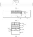
- FIG. 2 is a cutaway drawing of a switching power module according to an embodiment of this application.
- the switching power module provided in this embodiment of this application includes a substrate 10, a die 20, and a packaging layer 30.
- the substrate 10 is configured to carry the die 20 and the packaging layer 30 as a carrying component.
- the packaging layer 30 is configured to protect security of the die 20 as a protection component of the die 20.
- the substrate 10 provided in this embodiment of this application may be a circuit board, and the substrate 10 has a circuit layer electrically connected to the die 20.
- the die 20 is embedded in the substrate 10, and can be connected to the circuit layer of the substrate 10 to form a circuit, to complete a function of the die 20.
- the die 20 has an integrated circuit layout layer (not shown in the figure).
- the integrated circuit layout layer is disposed on a surface of the die 20, and the integrated circuit layout layer is configured to be electrically connected to the circuit layer of the substrate 10.
- the packaging layer 30 is configured to package the integrated circuit layout layer of the die 20 to ensure security of the integrated circuit layout layer of the die 20.
- the packaging layer 30 includes a composite material layer covering the integrated circuit layout layer, and the composite material layer includes at least two material layers that have different functions. The following describes, in detail with reference to accompanying drawings, the at least two material layers of the composite material layer provided in this embodiment of this application.
- FIG. 3 is a schematic diagram of cooperation between the die and the packaging layer.
- the die 20 provided in this embodiment of this application is a bare die, and the integrated circuit layout layer 21 of the die 20 is a circuit on the die 20. It should be understood that there is a gap in the integrated circuit layout layer 21 of the die 20.
- Two metal protrusions of the integrated circuit layout layer 21 shown in FIG. 2 are used as an example.
- the two metal protrusions are a first cable 211 and a second cable 212.
- the first cable 211 and the second cable 212 each are a solid metal part of the integrated circuit layout layer 21.
- a gap between the first cable 211 and the second cable 212 is the gap of the integrated circuit layout layer 21.
- the packaging layer 30 covers the integrated circuit layout layer 21 of the die 20 during packaging.
- the packaging layer 30 provided in this embodiment of this application uses a three-layer structure.
- a first material layer 31 covers the die 20
- a second material layer 32 covers the first material layer 31, and a third material layer 33 covers the second material layer 32.
- the die 20 is sequentially covered by the first material layer 31, the second material layer 32, and the third material layer 33, to protect the die 20.
- the first material layer 31 When covering the die 20, the first material layer 31 covers the integrated circuit layout layer 21 of the die 20, and is filled in a gap between metal protrusions of the integrated circuit layout layer 21 to implement electrical isolation between internal components of the die 20.
- the first cable 211 and the second cable 212 are used as an example.
- the first material layer 31 has a protrusion filled in the gap between the first cable 211 and the second cable 212, and the protrusion physically isolates the first cable 211 and the second cable 212.
- the first material layer 31 is prepared by using an insulating material. Therefore, the formed protrusion electrically isolates the first cable 211 and the second cable 212.
- the first material layer 31 is formed as a mixed layer by using a mixture that is of undoped silicate glass (Undoped Silicate Glass) and tetraethyl orthosilicate and that is prepared by using a high-density plasma chemical vapor deposition method.
- a first layer of structure is prepared on the integrated circuit layout layer 21 by using the undoped silicate glass, and then a second layer of structure is prepared on the first layer of structure by using the tetraethyl orthosilicate.
- a ratio of the undoped silicate glass to the tetraethyl orthosilicate is greater than or equal to 5:9 and less than or equal to 10:3.
- the undoped silicate glass has good hole filling density and is relatively hard.
- the tetraethyl orthosilicate has good coverage and is relatively soft.
- the undoped silicate glass can tolerate a relatively large pressure like concrete, and the tetraethyl orthosilicate can absorb a part of a stress like a sponge, so that the first material layer 31 has both good hardness and good flexibility.
- the first material layer 31 can tolerate a temperature change between minus 40 degrees Celsius and 100 degrees Celsius, and can relatively rapidly absorb heat generated by the die 20, to avoid deformation of the first material layer 31 due to the heat generated by the die 20, thereby reducing a cracking risk of the first material layer 31.
- a thickness of the first material layer 31 may be greater than or equal to 3000 angstroms (300 nm) and less than or equal to 9000 angstroms (900 nm), to ensure that the first material layer 31 has an enough thickness to improve a thermal stress effect of the packaging layer 30.
- the thickness of the first material layer 31 may be any thickness greater than or equal to 3000 angstroms (300 nm) and less than or equal to 9000 angstroms (900 nm), such as 3000 angstroms (300 nm), 3500 angstroms (350 nm), 4000 angstroms (400 nm), 4500 angstroms (450 nm), 5000 angstroms (500 nm), 5600 angstroms (560 nm), 6000 angstroms (600 nm), 6400 angstroms (640 nm), 7000 angstroms (700 nm), 7500 angstroms (750 nm), 8000 angstroms (800 nm), 8500 angstroms (850 nm), or 9000 angstroms (900 nm).
- the first material layer 31 may be directly prepared on the die 20 in a chemical deposition manner.
- the first material layer 31 is prepared on the die 20 through high-density plasma chemical vapor deposition.
- the undoped silicate glass is mixed with the tetraethyl orthosilicate, and then the mixture is prepared on the die 20 through high-density plasma chemical vapor deposition.
- the first material layer 31 covers the integrated circuit layout layer 21 of the die 20.
- the composite material layer further includes the second material layer 32, and both a material and a function of the second material layer 32 are different from those of the first material layer 31.
- the second material layer 32 covers the first material layer 31, and a material of the second material layer 32 may be silicon oxynitride or tetraethyl orthosilicate.
- the second material layer 32 is stacked with the first material layer 31, and is located on a surface that is of the first material layer 31 and that faces away from the die 20.
- the second material layer 32 may be formed on the first material layer 31 in a manner of chemical vapor deposition and coating and curing, so that the second material layer 32 can be securely connected to the first material layer 31.
- Both the silicon oxynitride and the tetraethyl orthosilicate have advantages such as thermal shock resistance, oxidation resistance, high density, an excellent mechanical property, and an excellent chemical stability, and are excellent high-temperature structural materials.
- the second material layer 32 prepared by using the silicon oxynitride or the tetraethyl orthosilicate can absorb a stress and the heat generated by the die 20, to effectively protect the first material layer 31.
- the second material layer 32 has a good thermal shock resistance property, so that the packaging layer 30 can well protect the die 20 when the temperature difference of the die 20 sharply changes or the temperature difference period of the die 20 changes.
- a thickness of the second material layer 32 is greater than or equal to 1000 angstroms (100 nm) and less than or equal to 3000 angstroms (300 nm), to ensure that the second material layer 32 has an enough thickness to improve a thermal stress effect of the packaging layer 30.
- the thickness of the second material layer 32 may be any thickness greater than or equal to 1000 angstroms (100 nm) and less than or equal to 3000 angstroms (300 nm), such as 1000 angstroms (100 nm), 1300 angstroms (130 nm), 1700 angstroms (170 nm), 2000 angstroms (200 nm), 2100 angstroms (210 nm), 2300 angstroms (230 nm), 2500 angstroms (250 nm), 2700 angstroms (270 nm), or 3000 angstroms (300 nm).
- the composite material layer may further include the third material layer 33.
- the third material layer 33 covers the second material layer 32, and a material of the third material layer 33 may be ultraviolet silicon nitride (UVSIN).
- UVSIN ultraviolet silicon nitride
- the third material layer 33 is stacked with the second material layer 32 during disposition, and is located on a surface that is of the second material layer 32 and that faces away from the first material layer 31.
- the third material layer 33 may be directly formed on the second material layer 32 in a sputtering manner, so that the third material layer 33 can be securely connected to the first material layer 31.
- the third material layer has good thermal shock resistance and good chemical stability because of being made of the ultraviolet silicon nitride.
- a thickness of the third material layer 33 is greater than or equal to 2000 angstroms (200 nm) and less than or equal to 6000 angstroms (600 nm), to ensure that the third material layer 33 has an enough thickness to improve a thermal stress effect of the packaging layer 30.
- the thickness of the third material layer 33 may be any thickness greater than or equal to 2000 angstroms (200 nm) and less than or equal to 6000 angstroms (600 nm), such as 2000 angstroms (200 nm), 2500 angstroms (250 nm), 3000 angstroms (300 nm), 3700 angstroms (370 nm), 4000 angstroms (400 nm), 4300 angstroms (430 nm), 5200 angstroms (520 nm), 5700 angstroms (570 nm), or 6000 angstroms (600 nm).
- a height of the packaging layer 30 can be controlled to be greater than or equal to 6000 angstroms (600 nm) and less than or equal to 18000 angstroms (1800 nm).
- an overall thickness of the packaging layer 30 may be different thicknesses, such as 6000 angstroms (600 nm), 7000 angstroms (700 nm), 11000 angstroms (1100 nm), 11500 angstroms (1150 nm), 12000 angstroms (1200 nm), 12500 angstroms (1250 nm), 13000 angstroms (1300 nm), and 1800 angstroms (180 nm).
- the composite material layer included in the packaging layer provided in this embodiment of this application is not limited to the three-layer material layer shown in FIG. 3 , and may be alternatively a material layer of another layer quantity as required.
- temperature cycle reliability tests are performed on the packaging layer 30 shown in FIG. 3 and a packaging layer in the conventional technology to perform comparison.
- the packaging layer in the conventional technology uses four layers of materials.
- a material of a first layer covering a die is silicon dioxide or ethyl orthosilicate, and a thickness of the first layer is 2000 angstroms (200 nm) to 6000 angstroms (600 nm).
- a material of a second layer is silicon dioxide, and a thickness of the second layer is 2000 angstroms (200 nm) to 6000 angstroms (600 nm).
- a material of a third layer is tetraethyl orthosilicate, and a thickness of the third layer is 2000 angstroms (200 nm) to 6000 angstroms (600 nm).
- a material of a fourth layer is silicon nitride, and a thickness of the fourth layer is 3000 angstroms (300 nm) to 6000 angstroms (600 nm).
- a temperature cycle reliability test is performed on the packaging layer, when a temperature difference is greater than or equal to 60 degrees Celsius, the packaging layer is cracked. Therefore, a requirement of a current switching power module cannot be met.
- a temperature cycle reliability test is performed on the packaging layer 30 provided in this embodiment of this application, when a temperature around the packaging layer 30 provided in this embodiment of this application circulates between minus 40 degrees Celsius and 100 degrees Celsius, a temperature change rate is greater than or equal to 10 degrees Celsius per minute, and a stage of minus 40 degrees Celsius and a stage of 100 degrees Celsius each need to be maintained for at least 15 minutes, the packaging layer 30 is still kept uncracked.
- the switching power module is in a rating working area after being powered on, no power failure occurs in 1000 cycles.
- the packaging layer 30 provided in this embodiment of this application can have a good thermal stress effect through cooperation between the first material layer 31, the second material layer 32, and the third material layer 33. Therefore, under the premise of ensuring reliably of the die 20 during working, a quantity of layers of the packaging layer 30 is reduced, and a thickness of the packaging layer 30 is also reduced, thereby facilitating miniaturization development of the switching power module.
- Step 001 Cover an integrated circuit layout layer of a die with a first material layer.
- a first material layer 31 is directly prepared, through high-density plasma chemical vapor deposition, on a surface that is of a die 20 and that has an integrated circuit layout layer 21.
- the first material layer 31 covers the die 20
- the first material layer 31 covers the integrated circuit layout layer 21 of the die 20, and is filled in a gap between metal protrusions of the integrated circuit layout layer 21, to electrically isolate the adjacent metal protrusions.
- the two metal protrusions in FIG. 4 are used as an example.
- the two metal protrusions are a first cable 211 and a second cable 212.
- the first material layer 31 isprepared on the die 20 through high-density plasma chemical vapor deposition. During specific preparation, first, a first layer of structure is prepared on the integrated circuit layout layer 21 by using undoped silicate glass, and then a second layer of structure is prepared on the first layer of structure by using tetraethyl orthosilicate.
- the first material layer 31 further has a protrusion filled in a gap between the first cable 211 and the second cable 212, and the protrusion physically isolates the first cable 211 and the second cable 212.
- the undoped silicate glass and the tetraethyl orthosilicate of the first material layer 31 are mixed as an insulating material, so that the formed protrusion can electrically isolate the first cable 211 and the second cable 212.
- the first material layer 31 is formed as a mixed layer by using a mixture that is of the undoped silicate glass (Undoped Silicate Glass) and the tetraethyl orthosilicate and that is prepared by using a high-density plasma chemical vapor deposition method.
- a ratio of the undoped silicate glass to the tetraethyl orthosilicate is greater than or equal to 5:9 and less than or equal to 10:3.
- the undoped silicate glass has good hole filling density and is relatively hard.
- the tetraethyl orthosilicate has good coverage and is relatively soft.
- the undoped silicate glass When the undoped silicate glass is mixed with the tetraethyl orthosilicate, the undoped silicate glass can tolerate a relatively large pressure like concrete, and the tetraethyl orthosilicate can absorb a part of a stress like a sponge, so that the first material layer 31 has both good hardness and good flexibility.
- the first material layer 31 can tolerate a temperature change between minus 40 degrees Celsius and 100 degrees Celsius, and can relatively rapidly absorb heat generated by the die 20, to avoid deformation of the first material layer 31 due to the heat generated by the die 20, thereby reducing a cracking risk of the first material layer 31.
- a thickness of the first material layer 31 may be greater than or equal to 3000 angstroms (300 nm) and less than or equal to 9000 angstroms (900 nm), to ensure that the first material layer 31 has an enough thickness to improve a thermal stress effect of the packaging layer.
- the thickness of the first material layer 31 may be any thickness greater than or equal to 3000 angstroms (300 nm) and less than or equal to 9000 angstroms (900 nm), such as 3000 angstroms (300 nm), 3500 angstroms (350 nm), 4000 angstroms (400 nm), 4500 angstroms (450 nm), 5000 angstroms (500 nm), 5600 angstroms (560 nm), 6000 angstroms (600 nm), 6400 angstroms (640 nm), 7000 angstroms (700 nm), 7500 angstroms (750 nm), 8000 angstroms (800 nm), 8500 angstroms (850 nm), or 9000 angstroms (900 nm).
- Step 002 Form a second material layer on the first material layer.
- a surface of the first material layer 31 is covered with a second material layer 32, and a material of the second material layer 32 may be silicon oxynitride or tetraethyl orthosilicate.
- the second material layer 32 is stacked with the first material layer 31, and is located on a surface that is of the first material layer 31 and that faces away from the die.
- the second material layer 32 may be formed on the first material layer 31 in a manner of chemical vapor deposition and coating and curing, so that the second material layer 32 can be securely connected to the first material layer 31.
- Both the silicon oxynitride and the tetraethyl orthosilicate have advantages such as thermal shock resistance, oxidation resistance, high density, an excellent mechanical property, and an excellent chemical stability, and are excellent high-temperature structural materials.
- the second material layer 32 prepared by using the silicon oxynitride or the tetraethyl orthosilicate can absorb a stress and the heat generated by the die 20, to effectively protect the first material layer 31.
- the second material layer 32 has a good thermal shock resistance property, so that the packaging layer 30 can well protect the die 20 when the temperature difference of the die 20 sharply changes or the temperature difference period of the die 20 changes.
- a thickness of the second material layer 32 is greater than or equal to 1000 angstroms (100 nm), and less than or equal to 3000 angstroms (300 nm), to ensure that the second material layer 32 has an enough thickness to improve a thermal stress effect of the packaging layer.
- the thickness of the second material layer 32 may be any thickness greater than or equal to 1000 angstroms (100 nm), and less than or equal to 3000 angstroms (300 nm), such as 1000 angstroms (100 nm), 1300 angstroms (130 nm), 1700 angstroms (170 nm), 2000 angstroms (200 nm), 2100 angstroms (210 nm), 2300 angstroms (230 nm), 2500 angstroms (250 nm), 2700 angstroms (270 nm), or 3000 angstroms (300 nm).
- Step 003 Form a third material layer on the second material layer.
- the second material layer 32 is covered with a third material layer 33, and a material of the third material layer 33 may be ultraviolet silicon nitride (UVSIN).
- UVSIN ultraviolet silicon nitride
- the third material layer 33 covers a surface that is of the second material layer 32 and that faces away from the first material layer.
- the third material layer 33 may be directly formed on the second material layer 32 in a sputtering manner, so that the third material layer 33 can be securely connected to the first material layer.
- the third material layer has good thermal shock resistance and good chemical stability because of being made of the ultraviolet silicon nitride.
- a thickness of the third material layer 33 is greater than or equal to 2000 angstroms (200 nm) and less than or equal to 6000 angstroms (600 nm), to ensure that the third material layer 33 has an enough thickness to improve a thermal stress effect of the packaging layer.
- the thickness of the third material layer 33 may be any thickness greater than or equal to 2000 angstroms (200 nm) and less than or equal to 6000 angstroms (600 nm), such as 2000 angstroms (200 nm), 2500 angstroms (250 nm), 3000 angstroms (300 nm), 3700 angstroms (370 nm), 4000 angstroms (400 nm), 4300 angstroms (430 nm), 5200 angstroms (520 nm), 5700 angstroms (570 nm), or 6000 angstroms (600 nm).
- Step 004 Embed the die in a substrate.
- the die 20 with the packaging layer 30 is embedded in a substrate 10.
- the substrate 10 may be prepared in layers, and the die 20 and the packaging layer 30 are embedded in the substrate 10 during the preparation in layers.
- a hole may be disposed on the substrate 10 after the substrate 10 is prepared, and the die 20 and the packaging layer 30 are embedded in the hole.
- the integrated circuit layout layer 21 of the die 20 is connected to a circuit layer of the substrate 10.
- the circuit layer on a surface of the substrate 10 may be connected to the integrated circuit layout layer 21 of the die 20 by disposing a via.
- a via 11 is disposed on the substrate 10.
- the via 11 is electrically connected to the first cable 211 after passing through the packaging layer 30 (sequentially passing through the third material layer 33, the second material layer 32, and the first material layer 31), so that the first cable 211 is electrically connected to the circuit layer (not shown in the figure) on the surface of the substrate 10. It should be understood that in FIG. 7 , only one via 11 is used as an example.
- a quantity of vias 11 is not limited in this embodiment of this application, and different quantities of vias 11 may be set based on connection requirements of the die 20 and the substrate 10.
- a specific preparation manner of the via may be an existing preparation manner, and details are not described herein.
- the packaging layer 30 can have a good thermal stress effect through cooperation between the first material layer 31, the second material layer 32, and the third material layer 33. Therefore, under the premise of ensuring reliably of the die 20 during working, a quantity of layers of the packaging layer 30 is reduced, and a thickness of the packaging layer 30 is also reduced, thereby facilitating miniaturization development of the switching power module.
- An embodiment of this application further provides a communications device.
- the communications device includes the switching power module 200 according to any one of the foregoing embodiments, and a control component 100 connected to the switching power module 200.
- FIG. 8 is a block diagram of a communications device.
- the communications device includes a control component 100 and a switching power module 200.
- the control component 100 may send an instruction to control the switching power module 200 to be turned on or turned off, to control a working status of the communications device. It should be understood that a principle and a structure for controlling the switching power module 200 by the control component 100 are an existing common control manner, and details are not described herein.
- a mixed layer being the first material layer 31 disclosed in the present claimed independent claim 1, and formed by using undoped silicate glass and tetraethyl orthosilicate is filled in a gap between metal protrusions of an integrated circuit layout layer, thereby improving an isolation effect between the metal protrusions.
- the mixed layer of the undoped silicate glass and the tetraethyl orthosilicate has a good thermal stress effect. Therefore, when a relatively large temperature difference cycle change occurs during working of a die, a first material layer does not crack, thereby improving a protection effect for the die and also improving reliability of the die.
Landscapes
- Semiconductor Integrated Circuits (AREA)
- Physics & Mathematics (AREA)
- Engineering & Computer Science (AREA)
- Plasma & Fusion (AREA)
- Structures Or Materials For Encapsulating Or Coating Semiconductor Devices Or Solid State Devices (AREA)
- Internal Circuitry In Semiconductor Integrated Circuit Devices (AREA)
Description
- This application relates to the field of electronic technologies, and in particular, to a switching power module and a communications device.
- High power density and miniaturization are a technical development trend of a switching power module.
US 2020/185297 A1 discloses a semiconductor device includes a semiconductor body having a first main surface. The semiconductor body includes an active device area and an edge termination area at least partly surrounding the active device area. The semiconductor device further includes a contact electrode on the first main surface and electrically connected to the active device area. The semiconductor device further includes a passivation structure on the edge termination area and laterally extending into the active device area. The semiconductor device further includes an encapsulation structure on the passivation structure and covering a first edge of the passivation structure above the contact electrode. The passivation structure may comprise undoped silicate glass and tetraethyl orthosilicate.
US 2018/047673 A1 discloses a package includes a redistribution portion, a first portion, and a second portion. The first portion is coupled to the redistribution portion. The first portion includes a first switch comprising a plurality of switch interconnects, and a first encapsulation layer that at least partially encapsulates the first switch. The second portion is coupled to the first portion. The second portion includes a first plurality of filters. Each filter includes a plurality of filter interconnects. The second portion also includes a second encapsulation layer that at least partially encapsulates the first plurality of filters. The first portion includes a second switch positioned next to the first switch, where the first encapsulation layer at least partially encapsulates the second switch. The second portion includes a second plurality of filters positioned next to the first plurality of filters, where the second encapsulation layer at least partially encapsulates the second plurality of filters.
With application of a 5th generation communications technology, power density of a circuit board increases, power consumption of the circuit board also increases, and a daily temperature difference of the circuit board accordingly increases. Therefore, a demand for a switching power module with high power density and a long temperature cycle life is to greatly increase in the future. To ensure reliability of the switching power module during use, a passivation layer is disposed on a die of the circuit board to protect a circuit on the die. However, if a temperature change rate of a cyclic temperature around the switching power module is relatively large, for example, the temperature change rate is between minus 40 degrees Celsius and 100 degrees Celsius, the passivation layer in the conventional technology is prone to be cracked because of being in the temperature difference change for long time, causing a failure of the switching power module. Therefore, a requirement of the switching power supply module for long-time reliable operation under this temperature cycle condition cannot be met. - This application provides a switching power module and a communications device, to improve reliability of the switching power module and this claimed invention is described in the
independent product claim 1. - According to a first aspect, a switching power module is provided. The switching power module may be applied to the field of switching power modules. The switching power module includes a substrate, a die, and a packaging layer, wherein the die is embedded in the substrate, and the die has an integrated circuit layout layer; wherein the packaging layer is configured to package the integrated circuit layout layer of the die, the packaging layer comprising a composite material layer comprising at least a first material layer and a second material layer that have different functions, wherein the first material layer is formed, through high-density plasma deposition, on a surface of the die that faces away from the substrate (10) and covers the integrated circuit layout layer. The first material layer is a mixed layer of undoped silicate glass and tetraethyl orthosilicate, and the first material layer is filled in a gap between metal protrusions of the integrated circuit layout layer, thereby improving an isolation effect between the metal protrusions. A a mixing ratio of the mixed layer of the undoped silicate glass and the tetraethyl orthosilicate is greater than or equal to 5:9 and less than or equal to 10:3. The mixed layer of the undoped silicate glass and the tetraethyl orthosilicate has a good thermal stress effect. Therefore, when a relatively large temperature difference cycle change occurs during working of the die, the first material layer does not crack, thereby improving a protection effect for the die and also improving reliability of the die.
- The first material layer that uses the claimed ratio has a good thermal stress effect.
- In a specific implementable solution, a thickness of the first material layer is greater than or equal to 3000 angstroms (300nm) and less than or equal to 9000 angstroms (900 nm). When the thickness is used, it is ensured that the first material layer has a good thermal stress effect.
- In a specific implementable solution, a thickness of the first material layer is greater than or equal to 5600 angstroms (560 nm) and less than or equal to 6400 angstroms (640 nm). This ensures that the first material layer has a good thermal stress effect.
- In a specific implementable solution, a total thickness of the passivation layer is greater than or equal to 6000 angstroms (600 nm) and less than or equal to 18000 angstroms (1800nm). This improves a protection effect of the passivation layer for the die.
- According to a second aspect, a communication device is provided. The communications device includes the switching power module according to any one of the first aspect and the specific implementable solutions of the first aspect, and a control component connected to the switching power module, wherein the control component is configured to control the switching power module. Therefore, when a relatively large temperature difference cycle change occurs during working of a die, a first material layer does not crack, thereby improving a protection effect for the die and also improving reliability of the die.
-
-
FIG. 1 is a schematic diagram of a switching power module according to the art; -
FIG. 2 is a schematic diagram of a structure of a switching power module according to an embodiment of this application; -
FIG. 3 is a partially enlarged diagram of a switching power module according to an embodiment of this application; -
FIG. 4 to FIG. 7 are a preparation flowchart of die packaging according to an embodiment of this application; and -
FIG. 8 is a schematic block diagram of a communications device according to an embodiment of this application. - For ease of understanding, an application scenario of a switching power module provided in embodiments of this application is first described. The switching power module provided in embodiments of this application is applied to a communications device, and is configured to control working status switching of the communications device. In the conventional technology, high power density and miniaturization are a technical development trend of a switching power module.
- With application of a 5th generation communications technology, power density of a circuit board further increases, and consequently power consumption of the circuit board accordingly increases. When the circuit board is used, a daily temperature difference of the circuit board also accordingly increases. Therefore, a demand for a switching power module with high power density and a long temperature cycle life is to greatly increase.
- For high power density and miniaturization of the circuit board, currently there is a packaging manner applicable to a circuit board with high power density. A packaged die shown in
FIG. 1 includes asubstrate 2, and thesubstrate 2 may be an organic substrate. Abare die 1 and a passivation layer (not shown in the figure) that packages thebare die 1 are embedded in thesubstrate 2. The passivation layer is configured to implement electrical isolation between internal components of thedie 1 and also protect interconnection between the internal components, and further can protect the components in thedie 1 from being mechanically and chemically damaged. A material and a structure of the passivation layer greatly affect a stress release rate of the packaged die. The packaged die is disposed on acircuit board 3. The die 1 is electrically connected (not shown in the figure) to thecircuit board 3 to form a switching power module. When the switching power module is used and a temperature difference of the circuit board is relatively large, whether the passivation layer can well release a thermal stress directly affects reliability of the packaged die. - For example, a temperature cycle reliability test may be used to verify a temperature cycle life of the switching power module. A verification condition is usually as follows: A temperature circulates between minus 40 degrees Celsius and 100 degrees Celsius, a temperature change rate is greater than or equal to 10 degrees Celsius per minute, and a stage of minus 40 degrees Celsius and a stage of 100 degrees Celsius each need to be maintained for at least 15 minutes. In addition, when the switching power module is in a rating working area after being powered on, a power failure cannot occur during 1000 cycles. In this way, a temperature cycle tolerance of the passivation layer of the die is checked, and a determining basis is whether the passivation layer of the die is cracked. When a switching power module in the conventional technology is verified, under repeated actions of a thermal stress, a passivation layer is separated from a neighboring insulation layer on the die, and a metal layer of the die migrates under excitation of an electric potential difference, causing damage to the die. In view of this, embodiments of this application provide die packaging. The following describes the die packaging in detail with reference to specific accompanying drawings and embodiments.
-
FIG. 2 is a cutaway drawing of a switching power module according to an embodiment of this application. The switching power module provided in this embodiment of this application includes asubstrate 10, adie 20, and apackaging layer 30. Thesubstrate 10 is configured to carry the die 20 and thepackaging layer 30 as a carrying component. Thepackaging layer 30 is configured to protect security of the die 20 as a protection component of thedie 20. The following describes the switching power module with reference to accompanying drawings and specific embodiments. - The
substrate 10 provided in this embodiment of this application may be a circuit board, and thesubstrate 10 has a circuit layer electrically connected to thedie 20. During assembly, thedie 20 is embedded in thesubstrate 10, and can be connected to the circuit layer of thesubstrate 10 to form a circuit, to complete a function of thedie 20. - The
die 20 has an integrated circuit layout layer (not shown in the figure). The integrated circuit layout layer is disposed on a surface of the die 20, and the integrated circuit layout layer is configured to be electrically connected to the circuit layer of thesubstrate 10. - The
packaging layer 30 is configured to package the integrated circuit layout layer of the die 20 to ensure security of the integrated circuit layout layer of thedie 20. During disposition, thepackaging layer 30 includes a composite material layer covering the integrated circuit layout layer, and the composite material layer includes at least two material layers that have different functions. The following describes, in detail with reference to accompanying drawings, the at least two material layers of the composite material layer provided in this embodiment of this application. -
FIG. 3 is a schematic diagram of cooperation between the die and the packaging layer. The die 20 provided in this embodiment of this application is a bare die, and the integratedcircuit layout layer 21 of the die 20 is a circuit on thedie 20. It should be understood that there is a gap in the integratedcircuit layout layer 21 of thedie 20. Two metal protrusions of the integratedcircuit layout layer 21 shown inFIG. 2 are used as an example. The two metal protrusions are afirst cable 211 and asecond cable 212. Thefirst cable 211 and thesecond cable 212 each are a solid metal part of the integratedcircuit layout layer 21. A gap between thefirst cable 211 and thesecond cable 212 is the gap of the integratedcircuit layout layer 21. - The
packaging layer 30 covers the integratedcircuit layout layer 21 of the die 20 during packaging. Thepackaging layer 30 provided in this embodiment of this application uses a three-layer structure. Afirst material layer 31 covers thedie 20, asecond material layer 32 covers thefirst material layer 31, and athird material layer 33 covers thesecond material layer 32. Thedie 20 is sequentially covered by thefirst material layer 31, thesecond material layer 32, and thethird material layer 33, to protect thedie 20. - When covering the
die 20, thefirst material layer 31 covers the integratedcircuit layout layer 21 of the die 20, and is filled in a gap between metal protrusions of the integratedcircuit layout layer 21 to implement electrical isolation between internal components of thedie 20. Thefirst cable 211 and thesecond cable 212 are used as an example. Thefirst material layer 31 has a protrusion filled in the gap between thefirst cable 211 and thesecond cable 212, and the protrusion physically isolates thefirst cable 211 and thesecond cable 212. In addition, thefirst material layer 31 is prepared by using an insulating material. Therefore, the formed protrusion electrically isolates thefirst cable 211 and thesecond cable 212. - To improve a protection effect of the
packaging layer 30 for the die 20, thefirst material layer 31 is formed as a mixed layer by using a mixture that is of undoped silicate glass (Undoped Silicate Glass) and tetraethyl orthosilicate and that is prepared by using a high-density plasma chemical vapor deposition method. During preparation, first, a first layer of structure is prepared on the integratedcircuit layout layer 21 by using the undoped silicate glass, and then a second layer of structure is prepared on the first layer of structure by using the tetraethyl orthosilicate. According to the invention, a ratio of the undoped silicate glass to the tetraethyl orthosilicate is greater than or equal to 5:9 and less than or equal to 10:3. The undoped silicate glass has good hole filling density and is relatively hard. The tetraethyl orthosilicate has good coverage and is relatively soft. When the undoped silicate glass is mixed with the tetraethyl orthosilicate, the undoped silicate glass can tolerate a relatively large pressure like concrete, and the tetraethyl orthosilicate can absorb a part of a stress like a sponge, so that thefirst material layer 31 has both good hardness and good flexibility. When a temperature difference sharply changes or a temperature difference period changes, thefirst material layer 31 can tolerate a temperature change between minus 40 degrees Celsius and 100 degrees Celsius, and can relatively rapidly absorb heat generated by thedie 20, to avoid deformation of thefirst material layer 31 due to the heat generated by thedie 20, thereby reducing a cracking risk of thefirst material layer 31. - In an optional solution, a thickness of the
first material layer 31 may be greater than or equal to 3000 angstroms (300 nm) and less than or equal to 9000 angstroms (900 nm), to ensure that thefirst material layer 31 has an enough thickness to improve a thermal stress effect of thepackaging layer 30. For example, the thickness of thefirst material layer 31 may be any thickness greater than or equal to 3000 angstroms (300 nm) and less than or equal to 9000 angstroms (900 nm), such as 3000 angstroms (300 nm), 3500 angstroms (350 nm), 4000 angstroms (400 nm), 4500 angstroms (450 nm), 5000 angstroms (500 nm), 5600 angstroms (560 nm), 6000 angstroms (600 nm), 6400 angstroms (640 nm), 7000 angstroms (700 nm), 7500 angstroms (750 nm), 8000 angstroms (800 nm), 8500 angstroms (850 nm), or 9000 angstroms (900 nm). - When the
first material layer 31 is specifically prepared, thefirst material layer 31 may be directly prepared on the die 20 in a chemical deposition manner. For example, thefirst material layer 31 is prepared on the die 20 through high-density plasma chemical vapor deposition. During specific preparation, first, the undoped silicate glass is mixed with the tetraethyl orthosilicate, and then the mixture is prepared on the die 20 through high-density plasma chemical vapor deposition. When thefirst material layer 31 is formed through deposition, thefirst material layer 31 covers the integratedcircuit layout layer 21 of thedie 20. - The composite material layer further includes the
second material layer 32, and both a material and a function of thesecond material layer 32 are different from those of thefirst material layer 31. During specific disposition, thesecond material layer 32 covers thefirst material layer 31, and a material of thesecond material layer 32 may be silicon oxynitride or tetraethyl orthosilicate. During disposition, thesecond material layer 32 is stacked with thefirst material layer 31, and is located on a surface that is of thefirst material layer 31 and that faces away from thedie 20. During preparation, thesecond material layer 32 may be formed on thefirst material layer 31 in a manner of chemical vapor deposition and coating and curing, so that thesecond material layer 32 can be securely connected to thefirst material layer 31. Both the silicon oxynitride and the tetraethyl orthosilicate have advantages such as thermal shock resistance, oxidation resistance, high density, an excellent mechanical property, and an excellent chemical stability, and are excellent high-temperature structural materials. Thesecond material layer 32 prepared by using the silicon oxynitride or the tetraethyl orthosilicate can absorb a stress and the heat generated by thedie 20, to effectively protect thefirst material layer 31. In addition, thesecond material layer 32 has a good thermal shock resistance property, so that thepackaging layer 30 can well protect the die 20 when the temperature difference of the die 20 sharply changes or the temperature difference period of the die 20 changes. - In an optional solution, a thickness of the
second material layer 32 is greater than or equal to 1000 angstroms (100 nm) and less than or equal to 3000 angstroms (300 nm), to ensure that thesecond material layer 32 has an enough thickness to improve a thermal stress effect of thepackaging layer 30. For example, the thickness of thesecond material layer 32 may be any thickness greater than or equal to 1000 angstroms (100 nm) and less than or equal to 3000 angstroms (300 nm), such as 1000 angstroms (100 nm), 1300 angstroms (130 nm), 1700 angstroms (170 nm), 2000 angstroms (200 nm), 2100 angstroms (210 nm), 2300 angstroms (230 nm), 2500 angstroms (250 nm), 2700 angstroms (270 nm), or 3000 angstroms (300 nm). - The composite material layer may further include the
third material layer 33. Thethird material layer 33 covers thesecond material layer 32, and a material of thethird material layer 33 may be ultraviolet silicon nitride (UVSIN). When thethird material layer 33 is prepared, thethird material layer 33 is stacked with thesecond material layer 32 during disposition, and is located on a surface that is of thesecond material layer 32 and that faces away from thefirst material layer 31. During preparation, thethird material layer 33 may be directly formed on thesecond material layer 32 in a sputtering manner, so that thethird material layer 33 can be securely connected to thefirst material layer 31. The third material layer has good thermal shock resistance and good chemical stability because of being made of the ultraviolet silicon nitride. - In an optional solution, a thickness of the
third material layer 33 is greater than or equal to 2000 angstroms (200 nm) and less than or equal to 6000 angstroms (600 nm), to ensure that thethird material layer 33 has an enough thickness to improve a thermal stress effect of thepackaging layer 30. For example, the thickness of thethird material layer 33 may be any thickness greater than or equal to 2000 angstroms (200 nm) and less than or equal to 6000 angstroms (600 nm), such as 2000 angstroms (200 nm), 2500 angstroms (250 nm), 3000 angstroms (300 nm), 3700 angstroms (370 nm), 4000 angstroms (400 nm), 4300 angstroms (430 nm), 5200 angstroms (520 nm), 5700 angstroms (570 nm), or 6000 angstroms (600 nm). - When the
packaging layer 30 is formed by using thefirst material layer 31, thesecond material layer 32, and thethird material layer 33, a height of thepackaging layer 30 can be controlled to be greater than or equal to 6000 angstroms (600 nm) and less than or equal to 18000 angstroms (1800 nm). For example, an overall thickness of thepackaging layer 30 may be different thicknesses, such as 6000 angstroms (600 nm), 7000 angstroms (700 nm), 11000 angstroms (1100 nm), 11500 angstroms (1150 nm), 12000 angstroms (1200 nm), 12500 angstroms (1250 nm), 13000 angstroms (1300 nm), and 1800 angstroms (180 nm). - It should be understood that the composite material layer included in the packaging layer provided in this embodiment of this application is not limited to the three-layer material layer shown in
FIG. 3 , and may be alternatively a material layer of another layer quantity as required. - To facilitate understanding of an effect of the
packaging layer 30 provided in this embodiment of this application, temperature cycle reliability tests are performed on thepackaging layer 30 shown inFIG. 3 and a packaging layer in the conventional technology to perform comparison. - The packaging layer in the conventional technology uses four layers of materials. A material of a first layer covering a die is silicon dioxide or ethyl orthosilicate, and a thickness of the first layer is 2000 angstroms (200 nm) to 6000 angstroms (600 nm). A material of a second layer is silicon dioxide, and a thickness of the second layer is 2000 angstroms (200 nm) to 6000 angstroms (600 nm). A material of a third layer is tetraethyl orthosilicate, and a thickness of the third layer is 2000 angstroms (200 nm) to 6000 angstroms (600 nm). A material of a fourth layer is silicon nitride, and a thickness of the fourth layer is 3000 angstroms (300 nm) to 6000 angstroms (600 nm). When a temperature cycle reliability test is performed on the packaging layer, when a temperature difference is greater than or equal to 60 degrees Celsius, the packaging layer is cracked. Therefore, a requirement of a current switching power module cannot be met.
- When a temperature cycle reliability test is performed on the
packaging layer 30 provided in this embodiment of this application, when a temperature around thepackaging layer 30 provided in this embodiment of this application circulates between minus 40 degrees Celsius and 100 degrees Celsius, a temperature change rate is greater than or equal to 10 degrees Celsius per minute, and a stage of minus 40 degrees Celsius and a stage of 100 degrees Celsius each need to be maintained for at least 15 minutes, thepackaging layer 30 is still kept uncracked. In addition, when the switching power module is in a rating working area after being powered on, no power failure occurs in 1000 cycles. - It can be learned from the comparison that, the
packaging layer 30 provided in this embodiment of this application can have a good thermal stress effect through cooperation between thefirst material layer 31, thesecond material layer 32, and thethird material layer 33. Therefore, under the premise of ensuring reliably of the die 20 during working, a quantity of layers of thepackaging layer 30 is reduced, and a thickness of thepackaging layer 30 is also reduced, thereby facilitating miniaturization development of the switching power module. - To facilitate understanding of the switching power module provided in this embodiment of this application, the following describes, in detail with reference to specific accompanying drawings, a method for preparing the switching power module shown in
FIG. 3 . - Step 001: Cover an integrated circuit layout layer of a die with a first material layer.
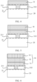
- As shown in
FIG. 4 , afirst material layer 31 is directly prepared, through high-density plasma chemical vapor deposition, on a surface that is of adie 20 and that has an integratedcircuit layout layer 21. When thefirst material layer 31 covers thedie 20, thefirst material layer 31 covers the integratedcircuit layout layer 21 of the die 20, and is filled in a gap between metal protrusions of the integratedcircuit layout layer 21, to electrically isolate the adjacent metal protrusions. - Two metal protrusions in
FIG. 4 are used as an example. The two metal protrusions are afirst cable 211 and asecond cable 212. Thefirst material layer 31 isprepared on the die 20 through high-density plasma chemical vapor deposition. During specific preparation, first, a first layer of structure is prepared on the integratedcircuit layout layer 21 by using undoped silicate glass, and then a second layer of structure is prepared on the first layer of structure by using tetraethyl orthosilicate. Thefirst material layer 31 further has a protrusion filled in a gap between thefirst cable 211 and thesecond cable 212, and the protrusion physically isolates thefirst cable 211 and thesecond cable 212. In addition, the undoped silicate glass and the tetraethyl orthosilicate of thefirst material layer 31 are mixed as an insulating material, so that the formed protrusion can electrically isolate thefirst cable 211 and thesecond cable 212. - To improve a protection effect of the
packaging layer 30 for the die 20, thefirst material layer 31 is formed as a mixed layer by using a mixture that is of the undoped silicate glass (Undoped Silicate Glass) and the tetraethyl orthosilicate and that is prepared by using a high-density plasma chemical vapor deposition method. According to the invention, a ratio of the undoped silicate glass to the tetraethyl orthosilicate is greater than or equal to 5:9 and less than or equal to 10:3. The undoped silicate glass has good hole filling density and is relatively hard. The tetraethyl orthosilicate has good coverage and is relatively soft. When the undoped silicate glass is mixed with the tetraethyl orthosilicate, the undoped silicate glass can tolerate a relatively large pressure like concrete, and the tetraethyl orthosilicate can absorb a part of a stress like a sponge, so that thefirst material layer 31 has both good hardness and good flexibility. When a temperature difference sharply changes or a temperature difference period changes, thefirst material layer 31 can tolerate a temperature change between minus 40 degrees Celsius and 100 degrees Celsius, and can relatively rapidly absorb heat generated by thedie 20, to avoid deformation of thefirst material layer 31 due to the heat generated by thedie 20, thereby reducing a cracking risk of thefirst material layer 31. - When the
first material layer 31 is specifically disposed, a thickness of thefirst material layer 31 may be greater than or equal to 3000 angstroms (300 nm) and less than or equal to 9000 angstroms (900 nm), to ensure that thefirst material layer 31 has an enough thickness to improve a thermal stress effect of the packaging layer. For example, the thickness of thefirst material layer 31 may be any thickness greater than or equal to 3000 angstroms (300 nm) and less than or equal to 9000 angstroms (900 nm), such as 3000 angstroms (300 nm), 3500 angstroms (350 nm), 4000 angstroms (400 nm), 4500 angstroms (450 nm), 5000 angstroms (500 nm), 5600 angstroms (560 nm), 6000 angstroms (600 nm), 6400 angstroms (640 nm), 7000 angstroms (700 nm), 7500 angstroms (750 nm), 8000 angstroms (800 nm), 8500 angstroms (850 nm), or 9000 angstroms (900 nm). - Step 002: Form a second material layer on the first material layer.
- As shown in
FIG. 5 , for some reference signs inFIG. 5 , refer to the same reference signs inFIG. 4 . A surface of thefirst material layer 31 is covered with asecond material layer 32, and a material of thesecond material layer 32 may be silicon oxynitride or tetraethyl orthosilicate. During disposition, thesecond material layer 32 is stacked with thefirst material layer 31, and is located on a surface that is of thefirst material layer 31 and that faces away from the die. During preparation, thesecond material layer 32 may be formed on thefirst material layer 31 in a manner of chemical vapor deposition and coating and curing, so that thesecond material layer 32 can be securely connected to thefirst material layer 31. - Both the silicon oxynitride and the tetraethyl orthosilicate have advantages such as thermal shock resistance, oxidation resistance, high density, an excellent mechanical property, and an excellent chemical stability, and are excellent high-temperature structural materials. The
second material layer 32 prepared by using the silicon oxynitride or the tetraethyl orthosilicate can absorb a stress and the heat generated by thedie 20, to effectively protect thefirst material layer 31. In addition, thesecond material layer 32 has a good thermal shock resistance property, so that thepackaging layer 30 can well protect the die 20 when the temperature difference of the die 20 sharply changes or the temperature difference period of the die 20 changes. - In an optional solution, a thickness of the
second material layer 32 is greater than or equal to 1000 angstroms (100 nm), and less than or equal to 3000 angstroms (300 nm), to ensure that thesecond material layer 32 has an enough thickness to improve a thermal stress effect of the packaging layer. For example, the thickness of thesecond material layer 32 may be any thickness greater than or equal to 1000 angstroms (100 nm), and less than or equal to 3000 angstroms (300 nm), such as 1000 angstroms (100 nm), 1300 angstroms (130 nm), 1700 angstroms (170 nm), 2000 angstroms (200 nm), 2100 angstroms (210 nm), 2300 angstroms (230 nm), 2500 angstroms (250 nm), 2700 angstroms (270 nm), or 3000 angstroms (300 nm). - Step 003: Form a third material layer on the second material layer.
- As shown in
FIG. 6 , for some reference signs inFIG. 6 , refer to the same reference signs inFIG. 5 . Thesecond material layer 32 is covered with athird material layer 33, and a material of thethird material layer 33 may be ultraviolet silicon nitride (UVSIN). When thethird material layer 33 is prepared, thethird material layer 33 covers a surface that is of thesecond material layer 32 and that faces away from the first material layer. Thethird material layer 33 may be directly formed on thesecond material layer 32 in a sputtering manner, so that thethird material layer 33 can be securely connected to the first material layer. The third material layer has good thermal shock resistance and good chemical stability because of being made of the ultraviolet silicon nitride. - In an optional solution, a thickness of the
third material layer 33 is greater than or equal to 2000 angstroms (200 nm) and less than or equal to 6000 angstroms (600 nm), to ensure that thethird material layer 33 has an enough thickness to improve a thermal stress effect of the packaging layer. For example, the thickness of thethird material layer 33 may be any thickness greater than or equal to 2000 angstroms (200 nm) and less than or equal to 6000 angstroms (600 nm), such as 2000 angstroms (200 nm), 2500 angstroms (250 nm), 3000 angstroms (300 nm), 3700 angstroms (370 nm), 4000 angstroms (400 nm), 4300 angstroms (430 nm), 5200 angstroms (520 nm), 5700 angstroms (570 nm), or 6000 angstroms (600 nm). - Step 004: Embed the die in a substrate.
- As shown in
FIG. 7 , for some reference signs inFIG. 7 , refer to the same reference signs inFIG. 6 . The die 20 with thepackaging layer 30 is embedded in asubstrate 10. Specifically, thesubstrate 10 may be prepared in layers, and thedie 20 and thepackaging layer 30 are embedded in thesubstrate 10 during the preparation in layers. Alternatively, a hole may be disposed on thesubstrate 10 after thesubstrate 10 is prepared, and thedie 20 and thepackaging layer 30 are embedded in the hole. - In addition, when the
die 20 is embedded in thesubstrate 10, the integratedcircuit layout layer 21 of the die 20 is connected to a circuit layer of thesubstrate 10. Specifically, the circuit layer on a surface of thesubstrate 10 may be connected to the integratedcircuit layout layer 21 of the die 20 by disposing a via. For example, a via 11 is disposed on thesubstrate 10. The via 11 is electrically connected to thefirst cable 211 after passing through the packaging layer 30 (sequentially passing through thethird material layer 33, thesecond material layer 32, and the first material layer 31), so that thefirst cable 211 is electrically connected to the circuit layer (not shown in the figure) on the surface of thesubstrate 10. It should be understood that inFIG. 7 , only one via 11 is used as an example. A quantity ofvias 11 is not limited in this embodiment of this application, and different quantities ofvias 11 may be set based on connection requirements of thedie 20 and thesubstrate 10. In addition, a specific preparation manner of the via may be an existing preparation manner, and details are not described herein. - In the switching power module prepared by using the preparation method, the
packaging layer 30 can have a good thermal stress effect through cooperation between thefirst material layer 31, thesecond material layer 32, and thethird material layer 33. Therefore, under the premise of ensuring reliably of the die 20 during working, a quantity of layers of thepackaging layer 30 is reduced, and a thickness of thepackaging layer 30 is also reduced, thereby facilitating miniaturization development of the switching power module. - An embodiment of this application further provides a communications device. The communications device includes the switching
power module 200 according to any one of the foregoing embodiments, and acontrol component 100 connected to the switchingpower module 200.FIG. 8 is a block diagram of a communications device. The communications device includes acontrol component 100 and a switchingpower module 200. Thecontrol component 100 may send an instruction to control the switchingpower module 200 to be turned on or turned off, to control a working status of the communications device. It should be understood that a principle and a structure for controlling the switchingpower module 200 by thecontrol component 100 are an existing common control manner, and details are not described herein. - In the switching power module, a mixed layer being the
first material layer 31 disclosed in the present claimedindependent claim 1, and formed by using undoped silicate glass and tetraethyl orthosilicate is filled in a gap between metal protrusions of an integrated circuit layout layer, thereby improving an isolation effect between the metal protrusions. In addition, the mixed layer of the undoped silicate glass and the tetraethyl orthosilicate has a good thermal stress effect. Therefore, when a relatively large temperature difference cycle change occurs during working of a die, a first material layer does not crack, thereby improving a protection effect for the die and also improving reliability of the die. - Certainly, a person skilled in the art can make various modifications and variations to this application without departing from the protection scope of this application. This application is intended to cover these modifications and variations of this application provided that they fall within the scope of protection defined by the following claims and their equivalent technologies.
Claims (4)
- A switching power module (200), comprising a substrate (10), a die (20), and a packaging layer (30), wherein the die (20) is embedded in the substrate (10), and the die (20) has an integrated circuit layout layer; whereinthe packaging layer (30) is configured to package the integrated circuit layout layer of the die (20), the packaging layer (30) comprising a composite material layer comprising at least a first material layer (31) and a second material layer (32) that have different functions, wherein the first material layer (31) is formed, through high-density plasma deposition, on a surface of the die that faces away from the substrate (10) and covers the integrated circuit layout layer, wherein the first material layer (31) is a mixed layer of undoped silicate glass and tetraethyl orthosilicate, and the first material layer (31) is filled in a gap between metal protrusions (211, 212) of the integrated circuit layout layer; andcharacterized in thata mixing ratio of the mixed layer of the undoped silicate glass and the tetraethyl orthosilicate is greater than or equal to 5:9 and less than or equal to 10:3.
- The switching power module (200) according to claim 1, wherein a thickness of the first material layer (31) is greater than or equal to 300 nm and less than or equal to 900 nm.
- The switching power module (200) according to claim 1 or 2, wherein a total thickness of the packaging layer (30) is greater than or equal to 600 nm and less than or equal to 1800 nm.
- A communication device, comprising the switching power module (200) according to any one of claims 1 to 3, and a control component connected (100) to the switching power module (200), wherein the control component (100) is configured to control the switching power module (200).
Applications Claiming Priority (1)
| Application Number | Priority Date | Filing Date | Title |
|---|---|---|---|
| PCT/CN2020/112652 WO2022041228A1 (en) | 2020-08-31 | 2020-08-31 | Switch power supply module and communication device |
Publications (3)
| Publication Number | Publication Date |
|---|---|
| EP4068341A1 EP4068341A1 (en) | 2022-10-05 |
| EP4068341A4 EP4068341A4 (en) | 2023-06-14 |
| EP4068341B1 true EP4068341B1 (en) | 2024-10-16 |
Family
ID=80354378
Family Applications (1)
| Application Number | Title | Priority Date | Filing Date |
|---|---|---|---|
| EP20950897.7A Active EP4068341B1 (en) | 2020-08-31 | 2020-08-31 | Switch power supply module and communication device |
Country Status (4)
| Country | Link |
|---|---|
| US (1) | US12610852B2 (en) |
| EP (1) | EP4068341B1 (en) |
| CN (1) | CN114450777B (en) |
| WO (1) | WO2022041228A1 (en) |
Citations (1)
| Publication number | Priority date | Publication date | Assignee | Title |
|---|---|---|---|---|
| JP2000286261A (en) * | 1999-01-27 | 2000-10-13 | Sony Corp | Method for forming insulating film and method for manufacturing semiconductor device |
Family Cites Families (15)
| Publication number | Priority date | Publication date | Assignee | Title |
|---|---|---|---|---|
| US6420777B2 (en) * | 1998-02-26 | 2002-07-16 | International Business Machines Corporation | Dual layer etch stop barrier |
| US6803327B1 (en) * | 1999-04-05 | 2004-10-12 | Taiwan Semiconductor Manufacturing Company | Cost effective polymide process to solve passivation extrusion or damage and SOG delminates |
| US6521975B1 (en) * | 1999-05-20 | 2003-02-18 | Texas Instruments Incorporated | Scribe street seals in semiconductor devices and method of fabrication |
| US7582556B2 (en) * | 2005-06-24 | 2009-09-01 | Megica Corporation | Circuitry component and method for forming the same |
| US7651891B1 (en) * | 2007-08-09 | 2010-01-26 | National Semiconductor Corporation | Integrated circuit package with stress reduction |
| US8058677B2 (en) * | 2008-06-26 | 2011-11-15 | Texas Instruments Incorporated | Stress buffer layer for ferroelectric random access memory |
| JP5335931B2 (en) * | 2008-12-26 | 2013-11-06 | メギカ・コーポレイション | Chip package with power management integrated circuit and related technology |
| US9728529B2 (en) * | 2014-04-14 | 2017-08-08 | Infineon Technologies Dresden Gmbh | Semiconductor device with electrostatic discharge protection structure |
| US9691637B2 (en) * | 2015-10-07 | 2017-06-27 | Nxp Usa, Inc. | Method for packaging an integrated circuit device with stress buffer |
| US10062630B2 (en) * | 2015-12-31 | 2018-08-28 | Infineon Technologies Austria Ag | Water and ion barrier for the periphery of III-V semiconductor dies |
| US10312193B2 (en) * | 2016-08-12 | 2019-06-04 | Qualcomm Incorporated | Package comprising switches and filters |
| US10103696B1 (en) * | 2017-04-13 | 2018-10-16 | Tagore Technology, Inc. | Integrated gallium nitride power amplifier and switch |
| CN107256833B (en) | 2017-07-07 | 2019-06-28 | 上海华虹宏力半导体制造有限公司 | Passivation layer of chip and method of forming passivation layer of chip |
| KR102599050B1 (en) * | 2018-08-20 | 2023-11-06 | 삼성전자주식회사 | Method of manufacturing semiconductor chip |
| DE102019131238B4 (en) * | 2018-12-06 | 2025-09-18 | Infineon Technologies Ag | Semiconductor device containing passivation structure and manufacturing method |
-
2020
- 2020-08-31 WO PCT/CN2020/112652 patent/WO2022041228A1/en not_active Ceased
- 2020-08-31 EP EP20950897.7A patent/EP4068341B1/en active Active
- 2020-08-31 CN CN202080030179.9A patent/CN114450777B/en active Active
-
2022
- 2022-12-12 US US18/064,355 patent/US12610852B2/en active Active
Patent Citations (1)
| Publication number | Priority date | Publication date | Assignee | Title |
|---|---|---|---|---|
| JP2000286261A (en) * | 1999-01-27 | 2000-10-13 | Sony Corp | Method for forming insulating film and method for manufacturing semiconductor device |
Also Published As
| Publication number | Publication date |
|---|---|
| US12610852B2 (en) | 2026-04-21 |
| EP4068341A1 (en) | 2022-10-05 |
| CN114450777B (en) | 2024-01-30 |
| WO2022041228A1 (en) | 2022-03-03 |
| US20230112034A1 (en) | 2023-04-13 |
| CN114450777A (en) | 2022-05-06 |
| EP4068341A4 (en) | 2023-06-14 |
Similar Documents
| Publication | Publication Date | Title |
|---|---|---|
| TWI549222B (en) | Insulating structure, method of forming insulating structure, and wafer level isolator including the same | |
| CN1976014B (en) | Semiconductor device and its production method | |
| CN102132406B (en) | Semiconductor device including stress relaxation gaps for enhancing chip package interaction stability | |
| CN106611741B (en) | Dielectric stacking, isolating devices and method of forming isolated devices | |
| TWI311790B (en) | Semiconductor device having bonding pad above low-k kielectric film and manufacturing method therefor | |
| CN103875063B (en) | Semiconductor device, method for manufacturing same, and electronic component | |
| EP2720236B1 (en) | High-voltage integrated metal capacitor and fabrication method | |
| US20110089551A1 (en) | Semiconductor device with double-sided electrode structure and its manufacturing method | |
| KR101674057B1 (en) | Semiconductor chip structure having a complex reinforced insulator and method of fabricating the same | |
| CN101179057B (en) | bonding pad structure and manufacturing method thereof | |
| TW571415B (en) | Double side connected type semiconductor apparatus | |
| US8203198B2 (en) | Thin film capacitor device used for a decoupling capacitor and having a resistor inside | |
| US20250266366A1 (en) | Packaging structure, method for preparing packaging structure, and electronic device | |
| CN100530582C (en) | Semiconductor device and method of forming the same | |
| CN217361590U (en) | Terminal structure, power semiconductor device and electronic equipment | |
| US12610852B2 (en) | Switching power module and communications device | |
| CN109920772B (en) | Package structure and method for forming the same | |
| RU2002133754A (en) | METHOD FOR PRODUCING HYBRID ELECTRONIC MODULE | |
| JP2006080149A (en) | Stack structure of semiconductor device | |
| CN114758991A (en) | Chip packaging structure | |
| KR101038530B1 (en) | Semiconductor device comprising barrier metal and coating film and method for manufacturing same | |
| CN104347581B (en) | Semiconductor interconnection structure, semiconductor device comprising same, and preparation methods thereof | |
| CN103187384B (en) | A kind of metal dielectric layer and preparation method thereof and a kind of circuit board | |
| JP2007281289A (en) | Electronic component and manufacturing method thereof | |
| US20260033323A1 (en) | High voltage isolation with controlled discharge path |
Legal Events
| Date | Code | Title | Description |
|---|---|---|---|
| STAA | Information on the status of an ep patent application or granted ep patent |
Free format text: STATUS: THE INTERNATIONAL PUBLICATION HAS BEEN MADE |
|
| PUAI | Public reference made under article 153(3) epc to a published international application that has entered the european phase |
Free format text: ORIGINAL CODE: 0009012 |
|
| STAA | Information on the status of an ep patent application or granted ep patent |
Free format text: STATUS: REQUEST FOR EXAMINATION WAS MADE |
|
| 17P | Request for examination filed |
Effective date: 20220627 |
|
| AK | Designated contracting states |
Kind code of ref document: A1 Designated state(s): AL AT BE BG CH CY CZ DE DK EE ES FI FR GB GR HR HU IE IS IT LI LT LU LV MC MK MT NL NO PL PT RO RS SE SI SK SM TR |
|
| REG | Reference to a national code |
Ref country code: DE Ipc: H01L0023310000 Ref country code: DE Ref legal event code: R079 Ref document number: 602020039746 Country of ref document: DE Free format text: PREVIOUS MAIN CLASS: H01L0021560000 Ipc: H01L0023310000 |
|
| RIC1 | Information provided on ipc code assigned before grant |
Ipc: H01L 21/56 20060101ALN20230209BHEP Ipc: H01L 23/538 20060101ALI20230209BHEP Ipc: H01L 23/00 20060101ALI20230209BHEP Ipc: H01L 23/31 20060101AFI20230209BHEP |
|
| A4 | Supplementary search report drawn up and despatched |
Effective date: 20230516 |
|
| RIC1 | Information provided on ipc code assigned before grant |
Ipc: H01L 21/56 20060101ALN20230510BHEP Ipc: H01L 23/538 20060101ALI20230510BHEP Ipc: H01L 23/00 20060101ALI20230510BHEP Ipc: H01L 23/31 20060101AFI20230510BHEP |
|
| DAV | Request for validation of the european patent (deleted) | ||
| DAX | Request for extension of the european patent (deleted) | ||
| STAA | Information on the status of an ep patent application or granted ep patent |
Free format text: STATUS: EXAMINATION IS IN PROGRESS |
|
| 17Q | First examination report despatched |
Effective date: 20240223 |
|
| GRAP | Despatch of communication of intention to grant a patent |
Free format text: ORIGINAL CODE: EPIDOSNIGR1 |
|
| STAA | Information on the status of an ep patent application or granted ep patent |
Free format text: STATUS: GRANT OF PATENT IS INTENDED |
|
| RIC1 | Information provided on ipc code assigned before grant |
Ipc: H01L 21/60 20060101ALN20240503BHEP Ipc: H01L 23/538 20060101ALN20240503BHEP Ipc: H01L 21/56 20060101ALN20240503BHEP Ipc: H01L 23/31 20060101AFI20240503BHEP |
|
| INTG | Intention to grant announced |
Effective date: 20240527 |
|
| P01 | Opt-out of the competence of the unified patent court (upc) registered |
Free format text: CASE NUMBER: APP_36993/2024 Effective date: 20240620 |
|
| GRAS | Grant fee paid |
Free format text: ORIGINAL CODE: EPIDOSNIGR3 |
|
| GRAA | (expected) grant |
Free format text: ORIGINAL CODE: 0009210 |
|
| STAA | Information on the status of an ep patent application or granted ep patent |
Free format text: STATUS: THE PATENT HAS BEEN GRANTED |
|
| AK | Designated contracting states |
Kind code of ref document: B1 Designated state(s): AL AT BE BG CH CY CZ DE DK EE ES FI FR GB GR HR HU IE IS IT LI LT LU LV MC MK MT NL NO PL PT RO RS SE SI SK SM TR |
|
| REG | Reference to a national code |
Ref country code: GB Ref legal event code: FG4D |
|
| REG | Reference to a national code |
Ref country code: CH Ref legal event code: EP |
|
| REG | Reference to a national code |
Ref country code: IE Ref legal event code: FG4D |
|
| REG | Reference to a national code |
Ref country code: DE Ref legal event code: R096 Ref document number: 602020039746 Country of ref document: DE |
|
| REG | Reference to a national code |
Ref country code: LT Ref legal event code: MG9D |
|
| REG | Reference to a national code |
Ref country code: NL Ref legal event code: MP Effective date: 20241016 |
|
| REG | Reference to a national code |
Ref country code: AT Ref legal event code: MK05 Ref document number: 1733666 Country of ref document: AT Kind code of ref document: T Effective date: 20241016 |
|
| PG25 | Lapsed in a contracting state [announced via postgrant information from national office to epo] |
Ref country code: NL Free format text: LAPSE BECAUSE OF FAILURE TO SUBMIT A TRANSLATION OF THE DESCRIPTION OR TO PAY THE FEE WITHIN THE PRESCRIBED TIME-LIMIT Effective date: 20241016 |
|
| PG25 | Lapsed in a contracting state [announced via postgrant information from national office to epo] |
Ref country code: NL Free format text: LAPSE BECAUSE OF FAILURE TO SUBMIT A TRANSLATION OF THE DESCRIPTION OR TO PAY THE FEE WITHIN THE PRESCRIBED TIME-LIMIT Effective date: 20241016 |
|
| PG25 | Lapsed in a contracting state [announced via postgrant information from national office to epo] |
Ref country code: HR Free format text: LAPSE BECAUSE OF FAILURE TO SUBMIT A TRANSLATION OF THE DESCRIPTION OR TO PAY THE FEE WITHIN THE PRESCRIBED TIME-LIMIT Effective date: 20241016 Ref country code: PT Free format text: LAPSE BECAUSE OF FAILURE TO SUBMIT A TRANSLATION OF THE DESCRIPTION OR TO PAY THE FEE WITHIN THE PRESCRIBED TIME-LIMIT Effective date: 20250217 Ref country code: IS Free format text: LAPSE BECAUSE OF FAILURE TO SUBMIT A TRANSLATION OF THE DESCRIPTION OR TO PAY THE FEE WITHIN THE PRESCRIBED TIME-LIMIT Effective date: 20250216 |
|
| PG25 | Lapsed in a contracting state [announced via postgrant information from national office to epo] |
Ref country code: FI Free format text: LAPSE BECAUSE OF FAILURE TO SUBMIT A TRANSLATION OF THE DESCRIPTION OR TO PAY THE FEE WITHIN THE PRESCRIBED TIME-LIMIT Effective date: 20241016 |
|
| PG25 | Lapsed in a contracting state [announced via postgrant information from national office to epo] |
Ref country code: BG Free format text: LAPSE BECAUSE OF FAILURE TO SUBMIT A TRANSLATION OF THE DESCRIPTION OR TO PAY THE FEE WITHIN THE PRESCRIBED TIME-LIMIT Effective date: 20241016 |
|
| PG25 | Lapsed in a contracting state [announced via postgrant information from national office to epo] |
Ref country code: ES Free format text: LAPSE BECAUSE OF FAILURE TO SUBMIT A TRANSLATION OF THE DESCRIPTION OR TO PAY THE FEE WITHIN THE PRESCRIBED TIME-LIMIT Effective date: 20241016 |
|
| PG25 | Lapsed in a contracting state [announced via postgrant information from national office to epo] |
Ref country code: NO Free format text: LAPSE BECAUSE OF FAILURE TO SUBMIT A TRANSLATION OF THE DESCRIPTION OR TO PAY THE FEE WITHIN THE PRESCRIBED TIME-LIMIT Effective date: 20250116 |
|
| PG25 | Lapsed in a contracting state [announced via postgrant information from national office to epo] |
Ref country code: LV Free format text: LAPSE BECAUSE OF FAILURE TO SUBMIT A TRANSLATION OF THE DESCRIPTION OR TO PAY THE FEE WITHIN THE PRESCRIBED TIME-LIMIT Effective date: 20241016 Ref country code: AT Free format text: LAPSE BECAUSE OF FAILURE TO SUBMIT A TRANSLATION OF THE DESCRIPTION OR TO PAY THE FEE WITHIN THE PRESCRIBED TIME-LIMIT Effective date: 20241016 Ref country code: GR Free format text: LAPSE BECAUSE OF FAILURE TO SUBMIT A TRANSLATION OF THE DESCRIPTION OR TO PAY THE FEE WITHIN THE PRESCRIBED TIME-LIMIT Effective date: 20250117 |
|
| PG25 | Lapsed in a contracting state [announced via postgrant information from national office to epo] |
Ref country code: PL Free format text: LAPSE BECAUSE OF FAILURE TO SUBMIT A TRANSLATION OF THE DESCRIPTION OR TO PAY THE FEE WITHIN THE PRESCRIBED TIME-LIMIT Effective date: 20241016 |
|
| PG25 | Lapsed in a contracting state [announced via postgrant information from national office to epo] |
Ref country code: RS Free format text: LAPSE BECAUSE OF FAILURE TO SUBMIT A TRANSLATION OF THE DESCRIPTION OR TO PAY THE FEE WITHIN THE PRESCRIBED TIME-LIMIT Effective date: 20250116 |
|
| PG25 | Lapsed in a contracting state [announced via postgrant information from national office to epo] |
Ref country code: SM Free format text: LAPSE BECAUSE OF FAILURE TO SUBMIT A TRANSLATION OF THE DESCRIPTION OR TO PAY THE FEE WITHIN THE PRESCRIBED TIME-LIMIT Effective date: 20241016 |
|
| PG25 | Lapsed in a contracting state [announced via postgrant information from national office to epo] |
Ref country code: DK Free format text: LAPSE BECAUSE OF FAILURE TO SUBMIT A TRANSLATION OF THE DESCRIPTION OR TO PAY THE FEE WITHIN THE PRESCRIBED TIME-LIMIT Effective date: 20241016 |
|
| REG | Reference to a national code |
Ref country code: DE Ref legal event code: R097 Ref document number: 602020039746 Country of ref document: DE |
|
| PG25 | Lapsed in a contracting state [announced via postgrant information from national office to epo] |
Ref country code: EE Free format text: LAPSE BECAUSE OF FAILURE TO SUBMIT A TRANSLATION OF THE DESCRIPTION OR TO PAY THE FEE WITHIN THE PRESCRIBED TIME-LIMIT Effective date: 20241016 |
|
| PG25 | Lapsed in a contracting state [announced via postgrant information from national office to epo] |
Ref country code: RO Free format text: LAPSE BECAUSE OF FAILURE TO SUBMIT A TRANSLATION OF THE DESCRIPTION OR TO PAY THE FEE WITHIN THE PRESCRIBED TIME-LIMIT Effective date: 20241016 |
|
| PG25 | Lapsed in a contracting state [announced via postgrant information from national office to epo] |
Ref country code: SK Free format text: LAPSE BECAUSE OF FAILURE TO SUBMIT A TRANSLATION OF THE DESCRIPTION OR TO PAY THE FEE WITHIN THE PRESCRIBED TIME-LIMIT Effective date: 20241016 |
|
| PG25 | Lapsed in a contracting state [announced via postgrant information from national office to epo] |
Ref country code: CZ Free format text: LAPSE BECAUSE OF FAILURE TO SUBMIT A TRANSLATION OF THE DESCRIPTION OR TO PAY THE FEE WITHIN THE PRESCRIBED TIME-LIMIT Effective date: 20241016 |
|
| PG25 | Lapsed in a contracting state [announced via postgrant information from national office to epo] |
Ref country code: IT Free format text: LAPSE BECAUSE OF FAILURE TO SUBMIT A TRANSLATION OF THE DESCRIPTION OR TO PAY THE FEE WITHIN THE PRESCRIBED TIME-LIMIT Effective date: 20241016 |
|
| PLBE | No opposition filed within time limit |
Free format text: ORIGINAL CODE: 0009261 |
|
| STAA | Information on the status of an ep patent application or granted ep patent |
Free format text: STATUS: NO OPPOSITION FILED WITHIN TIME LIMIT |
|
| PG25 | Lapsed in a contracting state [announced via postgrant information from national office to epo] |
Ref country code: SE Free format text: LAPSE BECAUSE OF FAILURE TO SUBMIT A TRANSLATION OF THE DESCRIPTION OR TO PAY THE FEE WITHIN THE PRESCRIBED TIME-LIMIT Effective date: 20241016 |
|
| 26N | No opposition filed |
Effective date: 20250717 |
|
| PGFP | Annual fee paid to national office [announced via postgrant information from national office to epo] |
Ref country code: DE Payment date: 20250702 Year of fee payment: 6 |
|
| REG | Reference to a national code |
Ref country code: DE Ref legal event code: R079 Ref document number: 602020039746 Country of ref document: DE Free format text: PREVIOUS MAIN CLASS: H01L0023310000 Ipc: H10W0074100000 |
|
| REG | Reference to a national code |
Ref country code: CH Ref legal event code: H13 Free format text: ST27 STATUS EVENT CODE: U-0-0-H10-H13 (AS PROVIDED BY THE NATIONAL OFFICE) Effective date: 20260324 |
|
| PG25 | Lapsed in a contracting state [announced via postgrant information from national office to epo] |
Ref country code: MC Free format text: LAPSE BECAUSE OF FAILURE TO SUBMIT A TRANSLATION OF THE DESCRIPTION OR TO PAY THE FEE WITHIN THE PRESCRIBED TIME-LIMIT Effective date: 20241016 |
|
| PG25 | Lapsed in a contracting state [announced via postgrant information from national office to epo] |
Ref country code: LU Free format text: LAPSE BECAUSE OF NON-PAYMENT OF DUE FEES Effective date: 20250831 |
|
| PG25 | Lapsed in a contracting state [announced via postgrant information from national office to epo] |
Ref country code: CH Free format text: LAPSE BECAUSE OF NON-PAYMENT OF DUE FEES Effective date: 20250831 |
|
| GBPC | Gb: european patent ceased through non-payment of renewal fee |
Effective date: 20250831 |
|
| REG | Reference to a national code |
Ref country code: BE Ref legal event code: MM Effective date: 20250831 |
|
| PG25 | Lapsed in a contracting state [announced via postgrant information from national office to epo] |
Ref country code: LT Free format text: LAPSE BECAUSE OF FAILURE TO SUBMIT A TRANSLATION OF THE DESCRIPTION OR TO PAY THE FEE WITHIN THE PRESCRIBED TIME-LIMIT Effective date: 20241016 |
|
| PG25 | Lapsed in a contracting state [announced via postgrant information from national office to epo] |
Ref country code: GB Free format text: LAPSE BECAUSE OF NON-PAYMENT OF DUE FEES Effective date: 20250831 |
|
| PG25 | Lapsed in a contracting state [announced via postgrant information from national office to epo] |
Ref country code: IE Free format text: LAPSE BECAUSE OF NON-PAYMENT OF DUE FEES Effective date: 20250831 Ref country code: BE Free format text: LAPSE BECAUSE OF NON-PAYMENT OF DUE FEES Effective date: 20250831 |
|
| PG25 | Lapsed in a contracting state [announced via postgrant information from national office to epo] |
Ref country code: FR Free format text: LAPSE BECAUSE OF NON-PAYMENT OF DUE FEES Effective date: 20250831 |