EP4066047B1 - Lightguide optical element for polarization scrambling - Google Patents
Lightguide optical element for polarization scrambling Download PDFInfo
- Publication number
- EP4066047B1 EP4066047B1 EP20894867.9A EP20894867A EP4066047B1 EP 4066047 B1 EP4066047 B1 EP 4066047B1 EP 20894867 A EP20894867 A EP 20894867A EP 4066047 B1 EP4066047 B1 EP 4066047B1
- Authority
- EP
- European Patent Office
- Prior art keywords
- coating
- loe
- light
- substrate
- refractive index
- Prior art date
- Legal status (The legal status is an assumption and is not a legal conclusion. Google has not performed a legal analysis and makes no representation as to the accuracy of the status listed.)
- Active
Links
Images






Classifications
-
- G—PHYSICS
- G02—OPTICS
- G02B—OPTICAL ELEMENTS, SYSTEMS OR APPARATUS
- G02B6/00—Light guides; Structural details of arrangements comprising light guides and other optical elements, e.g. couplings
- G02B6/10—Light guides; Structural details of arrangements comprising light guides and other optical elements, e.g. couplings of the optical waveguide type
- G02B6/105—Light guides; Structural details of arrangements comprising light guides and other optical elements, e.g. couplings of the optical waveguide type having optical polarisation effects
-
- G—PHYSICS
- G02—OPTICS
- G02B—OPTICAL ELEMENTS, SYSTEMS OR APPARATUS
- G02B1/00—Optical elements characterised by the material of which they are made; Optical coatings for optical elements
- G02B1/10—Optical coatings produced by application to, or surface treatment of, optical elements
- G02B1/11—Anti-reflection coatings
-
- G—PHYSICS
- G02—OPTICS
- G02B—OPTICAL ELEMENTS, SYSTEMS OR APPARATUS
- G02B1/00—Optical elements characterised by the material of which they are made; Optical coatings for optical elements
- G02B1/10—Optical coatings produced by application to, or surface treatment of, optical elements
- G02B1/11—Anti-reflection coatings
- G02B1/113—Anti-reflection coatings using inorganic layer materials only
- G02B1/115—Multilayers
-
- G—PHYSICS
- G02—OPTICS
- G02B—OPTICAL ELEMENTS, SYSTEMS OR APPARATUS
- G02B27/00—Optical systems or apparatus not provided for by any of the groups G02B1/00 - G02B26/00, G02B30/00
- G02B27/0081—Optical systems or apparatus not provided for by any of the groups G02B1/00 - G02B26/00, G02B30/00 with means for altering, e.g. enlarging, the entrance or exit pupil
-
- G—PHYSICS
- G02—OPTICS
- G02B—OPTICAL ELEMENTS, SYSTEMS OR APPARATUS
- G02B27/00—Optical systems or apparatus not provided for by any of the groups G02B1/00 - G02B26/00, G02B30/00
- G02B27/01—Head-up displays
-
- G—PHYSICS
- G02—OPTICS
- G02B—OPTICAL ELEMENTS, SYSTEMS OR APPARATUS
- G02B6/00—Light guides; Structural details of arrangements comprising light guides and other optical elements, e.g. couplings
-
- G—PHYSICS
- G02—OPTICS
- G02B—OPTICAL ELEMENTS, SYSTEMS OR APPARATUS
- G02B6/00—Light guides; Structural details of arrangements comprising light guides and other optical elements, e.g. couplings
- G02B6/24—Coupling light guides
- G02B6/26—Optical coupling means
- G02B6/27—Optical coupling means with polarisation selective and adjusting means
- G02B6/2726—Optical coupling means with polarisation selective and adjusting means in or on light guides, e.g. polarisation means assembled in a light guide
- G02B6/2733—Light guides evanescently coupled to polarisation sensitive elements
-
- G—PHYSICS
- G02—OPTICS
- G02B—OPTICAL ELEMENTS, SYSTEMS OR APPARATUS
- G02B6/00—Light guides; Structural details of arrangements comprising light guides and other optical elements, e.g. couplings
- G02B6/24—Coupling light guides
- G02B6/26—Optical coupling means
- G02B6/27—Optical coupling means with polarisation selective and adjusting means
- G02B6/2753—Optical coupling means with polarisation selective and adjusting means characterised by their function or use, i.e. of the complete device
- G02B6/2766—Manipulating the plane of polarisation from one input polarisation to another output polarisation, e.g. polarisation rotators, linear to circular polarisation converters
-
- G—PHYSICS
- G02—OPTICS
- G02F—OPTICAL DEVICES OR ARRANGEMENTS FOR THE CONTROL OF LIGHT BY MODIFICATION OF THE OPTICAL PROPERTIES OF THE MEDIA OF THE ELEMENTS INVOLVED THEREIN; NON-LINEAR OPTICS; FREQUENCY-CHANGING OF LIGHT; OPTICAL LOGIC ELEMENTS; OPTICAL ANALOGUE/DIGITAL CONVERTERS
- G02F1/00—Devices or arrangements for the control of the intensity, colour, phase, polarisation or direction of light arriving from an independent light source, e.g. switching, gating or modulating; Non-linear optics
- G02F1/01—Devices or arrangements for the control of the intensity, colour, phase, polarisation or direction of light arriving from an independent light source, e.g. switching, gating or modulating; Non-linear optics for the control of the intensity, phase, polarisation or colour
- G02F1/0136—Devices or arrangements for the control of the intensity, colour, phase, polarisation or direction of light arriving from an independent light source, e.g. switching, gating or modulating; Non-linear optics for the control of the intensity, phase, polarisation or colour for the control of polarisation, e.g. state of polarisation [SOP] control, polarisation scrambling, TE-TM mode conversion or separation
-
- G—PHYSICS
- G02—OPTICS
- G02F—OPTICAL DEVICES OR ARRANGEMENTS FOR THE CONTROL OF LIGHT BY MODIFICATION OF THE OPTICAL PROPERTIES OF THE MEDIA OF THE ELEMENTS INVOLVED THEREIN; NON-LINEAR OPTICS; FREQUENCY-CHANGING OF LIGHT; OPTICAL LOGIC ELEMENTS; OPTICAL ANALOGUE/DIGITAL CONVERTERS
- G02F1/00—Devices or arrangements for the control of the intensity, colour, phase, polarisation or direction of light arriving from an independent light source, e.g. switching, gating or modulating; Non-linear optics
- G02F1/01—Devices or arrangements for the control of the intensity, colour, phase, polarisation or direction of light arriving from an independent light source, e.g. switching, gating or modulating; Non-linear optics for the control of the intensity, phase, polarisation or colour
- G02F1/0136—Devices or arrangements for the control of the intensity, colour, phase, polarisation or direction of light arriving from an independent light source, e.g. switching, gating or modulating; Non-linear optics for the control of the intensity, phase, polarisation or colour for the control of polarisation, e.g. state of polarisation [SOP] control, polarisation scrambling, TE-TM mode conversion or separation
- G02F1/0139—Polarisation scrambling devices; Depolarisers
Definitions
- the presently disclosed subject matter relates to a lightguide optical element, and, more particularly, to a lightguide optical element configured for polarization scrambling.
- the present invention relates to light-guide compact collimating optical devices (LCCDs) and to optical systems which include one or more of these devices.
- the term "light-guide” refers to any light-transmitting body, preferably light-transmitting, solid bodies, also known as optical substrates.
- One of the important applications for compact optical devices is in the field of Head Mounted Displays (HMD), wherein an optical module serves both as a reflecting optical element and a combiner, in which a two-dimensional image is imaged to infinity and reflected into the eye of an observer.
- HMD Head Mounted Displays
- the image can be obtained directly from a spatial light modulator (SLM), such as a cathode ray tube (CRT), a liquid crystal display (LCD), liquid crystal on silicone (LCOS) module, an organic light emitting diode array (OLED), micro-LED a scanning source or similar devices, or indirectly, by means of a relay lens or an optical fiber bundle.
- SLM spatial light modulator
- CTR cathode ray tube
- LCD liquid crystal display
- LCOS liquid crystal on silicone
- OLED organic light emitting diode array
- micro-LED micro-LED a scanning source or similar devices
- the image comprises an array of elements (pixels) imaged to infinity by a collimating lens and transmitted into the eye of the viewer by means of a reflecting or partially reflecting surface acting as a combiner for non-see-through and see-through applications, respectively.
- a conventional, free-space optical module is used for these purposes. This optical module will be referred to herein as a Lightguide Optical Element ("LO
- the LOE is positioned in front of the viewer's eye.
- a collimated beam of light rays entering the LOE is reflected between the parallel surfaces by total internal reflection ("TIR").
- TIR total internal reflection
- Coated facets partially reflect the rays towards the viewer's eye.
- the light entering the LOE is either S-polarized or P-polarized.
- the coatings on the facets reflect light having the same polarization state. Since there is only one polarization state involved, the TIR reflection will maintain this polarization state. However, in applications where the light entering the LOE is unpolarized, every TIR reflection causes a phase shift which will change the polarization state of some of the rays. This in turn can lead to a corresponding change in the amount of light reflected by the facets, which is undesirable.
- US2007159673 discloses an image-guiding substrate comprising an image output portion including a plurality of mirrors configured to receive propagated rays and launch the propagated rays toward a viewing region, each mirror having a partial reflectivity.
- WO2016075689 discloses an optical system including a light-transmitting substrate, an optical element for coupling light waves into the substrate, at least one partially reflecting surface located in the substrate, at least one transparent air gap film attached to one of the major surfaces of the substrate.
- WO2016103251 discloses an optical system that includes a light-transmitting substrate and an optical element for coupling light waves into the substrate, at least one partially reflecting surface located in the substrate for coupling light waves out of the substrate, and at least one transparent layer, having a refractive index substantially lower than the refractive index of the light transmitting substrate optically attached to at least one of the major surfaces of the substrate.
- WO0187634 discloses a thermally imageable layer comprising an aqueous dispersion containing an immiscible compound, typically a near infrared absorber, and a dispersant, typically an acrylic polymer, which layer is useful in laser induced colorant transfer processes.
- an immiscible compound typically a near infrared absorber
- a dispersant typically an acrylic polymer
- US3829197 discloses an antireflection multilayer coating deposited on a substrate having a refractive index higher than 1.60 and comprising at least five partial layers.
- a lightguide optical element configured for polarization scrambling including: a transparent substrate having a first refractive index, the substrate including a pair of parallel external surfaces configured to propagate light within the LOE through total internal reflection (TIR), and a plurality of mutually parallel partially reflective internal surfaces, the plurality of mutually parallel partially reflective internal surfaces being non-parallel to the pair of parallel external surfaces and configured to couple out the light to a viewer; a first coating having a thickness between 100nm and 10 microns on at least one external surface of the substrate, the first coating including a coating material having a second refractive index higher than the first refractive index; and an antireflective (AR) coating on at least one external surface of the substrate over the first coating.
- the first coating is configured to increase a phase shift between s-polarized and p-polarized components of light incident at angles above a TIR cutoff angle for the substrate, the light having a wavelength between 400nm and 1300n
- the AR coating is configured to reduce or eliminate reflections of light entering the LOE at angles of incidence between 0° and 50°.
- the AR coating is configured to reduce reflections of light entering the LOE at predetermined angles to between 0.3% and 10% reflected light.
- the first coating includes a high index dielectric material.
- the first coating includes a material selected from the group consisting of TiO 2 , Si 3 N 4 and ZnS.
- the AR coating includes one or more layers of at least one coating material selected from the group consisting of SiO 2 , HfO 2 , TiO 2 , MgF 2 and Al 2 O 3 .
- the AR coating includes one or more layers of at least one material having a refractive index in the range of 1.35 to 2.5.
- phase shift' refers to the difference between the phase of the S-polarized rays and P-polarized rays.
- Fig. 1 illustrating a generalized schematic diagram of a LOE according to the prior art.
- the LOE comprises a substrate 34 that has a pair of parallel external surfaces 26, 27, and a non-parallel set of mutually parallel partially reflective internal surfaces ("facets") 22.
- the partially reflective property of facets 22 is achieved via a coating applied to the facets.
- Light rays 18 representing an image is coupled into the LOE and propagates within the LOE via TIR between surfaces 26, 27, and are eventually reflected out by facets 22 towards the eye 24 of a viewer.
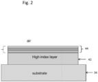
- Fig. 2 illustrates a generalized schematic diagram of an LOE according to certain embodiments of the presently disclosed subject matter.
- the LOE is intended to receive and couple out unpolarized light.
- the LOE of the present invention is comprised of a transparent substrate 34 having a refractive index (denoted herein as " n ") higher than air.
- the substrate comprises a pair of parallel external surfaces 26, 27 configured to propagate light within the LOE through TIR.
- Substrate 34 further comprises a plurality of mutually parallel partially reflective internal surfaces (“facets") 22 configured to couple out the light to a viewer.
- the facets are non-parallel to the external surfaces 26, 27. For example, they may be inclined relative to the pair of external surfaces.
- the LOE further includes a polarization scrambling coating 42 applied to at least one of surfaces 26, 27.
- Coating 42 is comprised of a coating material having a refractive index, which is higher than the first refractive index of substrate 34.
- the polarization scrambling coating 42 is applied to at least one of the external surfaces 26, 27, or a portion thereof, in a thickness greater than 100nm and up to about 10 microns. In some cases, the polarization scrambling coating 42 can be applied to both parallel external surfaces.
- the polarization scrambling coating 42 applied to the external surfaces of the substrate increases the phase difference slope between the S-polarized and P-polarized light rays entering the substrate and reflecting off the inside of the external coated surface. This is for angles of incidence above the Total Internal Reflection (TIR) angle.
- TIR Total Internal Reflection
- Polarization scrambling coating 42 can be selected according to predetermined design requirements based on the expected range of wavelengths of light entering the LOE and the expected range of angles at which the light will enter, for instance angles in the TIR region above 42° for BK7 glass. After a few reflections, the S-polarized light and P-polarized light propagating within the LOE will become greatly phase shifted with respect to one another, essentially maintaining the light rays' unpolarized state.
- the facets 22 within the LOE are also coated with a partially reflective coating designed for unpolarized light. These coated facets reflect the unpolarized light towards the viewer as designed.
- polarization scrambling coating 42 is applied in a thickness of between 300nm - 10000nm, and more preferably between 300nm - 5000nm, and even more preferably between 300nm - 1000nm.
- polarization scrambling coating 42 is comprised of a high index dielectric material such as TiO 2 ( n ⁇ 2.2-2.45), Si 3 N 4 , ( n ⁇ 2.0), ZnS ( n ⁇ 2.2-2.4) or suitable equivalents.
- high index it is meant a refractive index higher than of the substrate and preferably at least 2.
- coating 42 is configured to increase the phase shift slope of light having a wavelength between 400nm and 1300nm, and more preferably between 400nm and 750nm, upon reflection off of an external surface of the substrate.
- the AR coating 44 is required to reduce the reflection and also to maintain the depolarization properties induced by the polarization scrambling coating 42. These requirements increase the design complexity of the AR coating 44.
- AR coating 44 is comprised of layers of coating materials having a refractive index in the range of 1.35 to 2.5.
- the coating includes one or more high refractive index materials, one or more low refractive index materials, and one or more medium (i.e. between the high and the low) refractive index materials.
- AR coating 44 can be comprised of layers of one or more of SiO 2 ( n ⁇ 1.45-1.47), HfO 2 ( n ⁇ 2.0-2.1), TiO 2 ( n ⁇ 2.2-2.45), MgF 2 ( n ⁇ 1.35-1.37) and/or Al 2 O 3 ( n ⁇ 1.63-1.68).
- Fig. 2 is not drawn to scale, and in reality the thickness of substrate 34 is typically several orders of magnitude greater than that of coatings 42, 44.
- Fig. 3 illustrates a graph showing the phase shift performance of an LOE without the polarization scrambling coating.
- the LOE is made from of S-TIM8 glass ( n ⁇ 1.596) without coating 42 applied to the external surfaces.
- the phase shift is nearly constant for all wavelengths in the visible spectrum. This is undesirable, as will be described below.
- Fig. 5 illustrates a graph showing an example of the phase shift caused by polarization scrambling coating 42 applied to a substrate in reference to the spectral peaks of a RGB LED light.
- the coating 42 is comprised of TiO 2 , and was applied to a substrate 34 made of S-TIM8 glass.
- Fig. 5 shows the results of two different thicknesses of coating 42, i.e. 300nm and 1000nm, respectively. As shown in Fig. 5 , as the thickness of the layer is increased, the slope of the phase change in the visible wavelengths becomes larger.
- the spectral areas where the highest depolarization and slope should take place are indicated by dashed squares, and correspond to the spectral peaks of RGB LED.
- a small change in the wavelength of the light entering the LOE produces a large change in the phase shift. This is compared to the spectral range of the LED emission that illuminates the system.
- the polarization scrambling coating 42 causes different degrees of phase shift to parts of the narrow spectral peaks (at ⁇ 480nm, ⁇ 580nm and ⁇ 640nm for the RGB LED, and ⁇ 443nm for the white LED). Since the human eye integrates the intensity of the light of close wavelengths, this effect is comparable to viewing unpolarized light.
- the depolarization after the reflection is partial. Since the light is reflected by the external surfaces multiple times before being reflected by the facets 22, the accumulated depolarization of the light rays is relatively high.
- Fig. 6 illustrates a graph showing reflective properties of an exemplary polarization scrambling coating 42 without an AR coating 44.
- coating 42 was applied at two different layer thicknesses, 300nm and 1000nm, respectively. As shown, coating 42 tends to be highly reflective (average of about 20% per side in the visible wavelengths), causing undesirable attenuation of the view of the outside world through the LOE.
- Fig. 7a illustrates a graph showing an example of a differential phase shift on reflection of light entering a LOE of the present invention.
- the substrate is coated with a polarization scrambling coating 42 comprised of a thick TiO 2 layer, and an AR coating 44 on top of the polarization scrambling coating.
- the graph shows differential phase shift on reflection of light entering the LOE at angles of incidence of 55 degrees, in the visible wavelengths, for two different thicknesses of coating 42, i.e. 300nm and 1000nm, respectively.
- Fig. 7b illustrates a graph showing the phase shift on reflection using the same coatings as in Fig. 7a , with coating 42 applied in a thickness of 1000nm, for a variety of different angles in the TIR region.
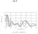
- Fig. 8 illustrates reflections at normal incidence of a coating of consisting of layers of coating 42 (300nm and 1000nm TiO2 layer thicknesses) and coating 44 as in Fig. 7a at different wavelengths in the visible spectrum. As shown in Fig. 8 , this coating performs as an AR coating at small angles, where it is apparent that the reflection is greatly reduced compared to Fig. 6 (from about 18% average in the visible spectrum to about 4%). Using different designs and layer material this reflection can be reduced even lower.
- the polarization scrambling coating 42 can be applied to only a portion of one or both external surfaces, instead of the entire surface.
- the LOE may be coated on one external surface, or a portion thereof, with a metallic coating.
- the polarization scrambling coating 42 can be added between the substrate and the metallic layer, which will increase the phase shift change over the spectral region.
- the rays entering the LOE may not be in the same plane of the drawing, i.e. entering the LOE at another three dimensional angle. In this case even if the beam is polarized, it will not be polarized in reference to the TIR planes. Therefore, it will change the polarization state of the reflected beam and can be treated as unpolarized light.
- Fig. 11 illustrates another embodiment of an LOE according to the present invention.
- the LOE is designed for light beams to enter at the center of the waveguide and propagate towards each opposite end.
- the incoming beam travels through a converging lens 6.
- Rays 641, and 64R pass through the LOE.
- the beams to the eye will either be transmitted through the center facets, or will be reflected by the central facets and travel to the side and reflected towards the eye by the other facets. Traveling from the central facets to the side facets, the rays encounter TIR from surfaces 1 and 2.
- surfaces 1 and 2 should also be coated with the polarization scrambling coating 42 (and optionally one or more layers of AR coating 44) for depolarizing the beams, since the next reflecting facets are designed for unpolarized light.
- the addition of AR layers will increase the transmittance of surfaces 1 and 2.
- embodiments of the presently described LOE can be implemented in a large number of imaging applications, such as head-mounted displays (HMDs) and head-up displays (HUDs), cellular phones, compact displays, 3-D displays, compact beam expanders, as well as non-imaging applications, such as flat-panel indicators, compact illuminators and scanners.
- imaging applications such as head-mounted displays (HMDs) and head-up displays (HUDs), cellular phones, compact displays, 3-D displays, compact beam expanders, as well as non-imaging applications, such as flat-panel indicators, compact illuminators and scanners.
Landscapes
- Physics & Mathematics (AREA)
- General Physics & Mathematics (AREA)
- Optics & Photonics (AREA)
- Nonlinear Science (AREA)
- Chemical & Material Sciences (AREA)
- Inorganic Chemistry (AREA)
- Polarising Elements (AREA)
- Surface Treatment Of Optical Elements (AREA)
- Surface Treatment Of Glass (AREA)
Description
- The presently disclosed subject matter relates to a lightguide optical element, and, more particularly, to a lightguide optical element configured for polarization scrambling.
- The present invention relates to light-guide compact collimating optical devices (LCCDs) and to optical systems which include one or more of these devices. The term "light-guide" refers to any light-transmitting body, preferably light-transmitting, solid bodies, also known as optical substrates. One of the important applications for compact optical devices is in the field of Head Mounted Displays (HMD), wherein an optical module serves both as a reflecting optical element and a combiner, in which a two-dimensional image is imaged to infinity and reflected into the eye of an observer. The image can be obtained directly from a spatial light modulator (SLM), such as a cathode ray tube (CRT), a liquid crystal display (LCD), liquid crystal on silicone (LCOS) module, an organic light emitting diode array (OLED), micro-LED a scanning source or similar devices, or indirectly, by means of a relay lens or an optical fiber bundle. The image comprises an array of elements (pixels) imaged to infinity by a collimating lens and transmitted into the eye of the viewer by means of a reflecting or partially reflecting surface acting as a combiner for non-see-through and see-through applications, respectively. Typically, a conventional, free-space optical module is used for these purposes. This optical module will be referred to herein as a Lightguide Optical Element ("LOE").
- Typically, the LOE is positioned in front of the viewer's eye. A collimated beam of light rays entering the LOE is reflected between the parallel surfaces by total internal reflection ("TIR"). Coated facets partially reflect the rays towards the viewer's eye.
- Typically, the light entering the LOE is either S-polarized or P-polarized. The coatings on the facets reflect light having the same polarization state. Since there is only one polarization state involved, the TIR reflection will maintain this polarization state. However, in applications where the light entering the LOE is unpolarized, every TIR reflection causes a phase shift which will change the polarization state of some of the rays. This in turn can lead to a corresponding change in the amount of light reflected by the facets, which is undesirable.
-
US2007159673 discloses an image-guiding substrate comprising an image output portion including a plurality of mirrors configured to receive propagated rays and launch the propagated rays toward a viewing region, each mirror having a partial reflectivity. -
WO2016075689 discloses an optical system including a light-transmitting substrate, an optical element for coupling light waves into the substrate, at least one partially reflecting surface located in the substrate, at least one transparent air gap film attached to one of the major surfaces of the substrate. -
WO2016103251 discloses an optical system that includes a light-transmitting substrate and an optical element for coupling light waves into the substrate, at least one partially reflecting surface located in the substrate for coupling light waves out of the substrate, and at least one transparent layer, having a refractive index substantially lower than the refractive index of the light transmitting substrate optically attached to at least one of the major surfaces of the substrate. -
WO0187634 -
US3829197 discloses an antireflection multilayer coating deposited on a substrate having a refractive index higher than 1.60 and comprising at least five partial layers. - According to one aspect of the presently disclosed subject matter there is provided a lightguide optical element (LOE) configured for polarization scrambling including: a transparent substrate having a first refractive index, the substrate including a pair of parallel external surfaces configured to propagate light within the LOE through total internal reflection (TIR), and a plurality of mutually parallel partially reflective internal surfaces, the plurality of mutually parallel partially reflective internal surfaces being non-parallel to the pair of parallel external surfaces and configured to couple out the light to a viewer; a first coating having a thickness between 100nm and 10 microns on at least one external surface of the substrate, the first coating including a coating material having a second refractive index higher than the first refractive index; and an antireflective (AR) coating on at least one external surface of the substrate over the first coating. The first coating is configured to increase a phase shift between s-polarized and p-polarized components of light incident at angles above a TIR cutoff angle for the substrate, the light having a wavelength between 400nm and 1300nm.
- In some embodiments the AR coating is configured to reduce or eliminate reflections of light entering the LOE at angles of incidence between 0° and 50°.
- In some embodiments the AR coating is configured to reduce reflections of light entering the LOE at predetermined angles to between 0.3% and 10% reflected light.
- In some embodiments the first coating includes a high index dielectric material.
- In some embodiments the first coating includes a material selected from the group consisting of TiO2, Si3N4 and ZnS.
- In some embodiments the AR coating includes one or more layers of at least one coating material selected from the group consisting of SiO2, HfO2, TiO2, MgF2 and Al2O3.
- In some embodiments the AR coating includes one or more layers of at least one material having a refractive index in the range of 1.35 to 2.5.
- In order to understand the invention and to see how it can be carried out in practice, embodiments will be described, by way of non-limiting examples, with reference to the accompanying drawings, in which:
-
Fig. 1 illustrates a generalized schematic diagram of a LOE according to the prior art; -
Fig. 2 illustrates a generalized schematic diagram of an LOE according to certain embodiments of the presently disclosed subject matter; -
Fig. 3 illustrates a graph showing an example of a phase shifting performance of one surface of the LOE without the polarization scrambling coating; -
Fig. 4a illustrates a graph showing the high spectral peaks of RGB light; -
Fig. 4b illustrates a graph showing the high spectral peaks of white light; -
Fig. 5 illustrates a graph showing an example of a spectral differential phase shift performance of a polarization scrambling coating applied to a substrate; -
Fig. 6 illustrates a graph showing reflective properties of an exemplary polarization scrambling coating without an AR coating at normal incidence; -
Fig. 7a illustrates a graph showing an example of a differential phase shift on reflection of light reflected by an LOE surface for rays in TIR; -
Fig. 7b illustrates a graph showing examples of differential phase shift on reflection for a variety of different angles in the TIR region; -
Fig. 8 illustrates a graph showing an example of reflections at normal incidence with the polarization scrambling coating and AR coating; -
Fig. 3 illustrates a graph showing an example of reflections of the polarization scrambling coating applied between the substrate and a metallic coating; -
Fig. 10 illustrates an embodiment of display system with two waveguides; and -
Fig. 11 illustrates another embodiment of an LOE according to the present invention. - In the following detailed description, numerous specific details are set forth in order to provide a thorough understanding of the invention. However, it will be understood by those skilled in the art that the presently disclosed subject matter may be practiced without these specific details. In other instances, well-known methods, procedures, and components have not been described in detail so as not to obscure the presently disclosed subject matter.
- As used herein, the term 'phase shift' refers to the difference between the phase of the S-polarized rays and P-polarized rays.
- Bearing this in mind, attention is drawn to
Fig. 1 illustrating a generalized schematic diagram of a LOE according to the prior art. The LOE comprises asubstrate 34 that has a pair of parallel external surfaces 26, 27, and a non-parallel set of mutually parallel partially reflective internal surfaces ("facets") 22. The partially reflective property of facets 22 is achieved via a coating applied to the facets. Light rays 18 representing an image is coupled into the LOE and propagates within the LOE via TIR between surfaces 26, 27, and are eventually reflected out by facets 22 towards the eye 24 of a viewer. -
Fig. 2 illustrates a generalized schematic diagram of an LOE according to certain embodiments of the presently disclosed subject matter. In this case, the LOE is intended to receive and couple out unpolarized light. As in the prior art LOE's, the LOE of the present invention is comprised of atransparent substrate 34 having a refractive index (denoted herein as "n") higher than air. The substrate comprises a pair of parallel external surfaces 26, 27 configured to propagate light within the LOE through TIR.Substrate 34 further comprises a plurality of mutually parallel partially reflective internal surfaces ("facets") 22 configured to couple out the light to a viewer. The facets are non-parallel to the external surfaces 26, 27. For example, they may be inclined relative to the pair of external surfaces. - The LOE further includes a
polarization scrambling coating 42 applied to at least one of surfaces 26, 27.Coating 42 is comprised of a coating material having a refractive index, which is higher than the first refractive index ofsubstrate 34. Thepolarization scrambling coating 42 is applied to at least one of the external surfaces 26, 27, or a portion thereof, in a thickness greater than 100nm and up to about 10 microns. In some cases, thepolarization scrambling coating 42 can be applied to both parallel external surfaces. Thepolarization scrambling coating 42 applied to the external surfaces of the substrate increases the phase difference slope between the S-polarized and P-polarized light rays entering the substrate and reflecting off the inside of the external coated surface. This is for angles of incidence above the Total Internal Reflection (TIR) angle. The phase difference slope is the amount of change of the phase shift difference for a small change of the wavelength. -
Polarization scrambling coating 42 can be selected according to predetermined design requirements based on the expected range of wavelengths of light entering the LOE and the expected range of angles at which the light will enter, for instance angles in the TIR region above 42° for BK7 glass. After a few reflections, the S-polarized light and P-polarized light propagating within the LOE will become greatly phase shifted with respect to one another, essentially maintaining the light rays' unpolarized state. According to this invention, the facets 22 within the LOE are also coated with a partially reflective coating designed for unpolarized light. These coated facets reflect the unpolarized light towards the viewer as designed. - In exemplary embodiments,
polarization scrambling coating 42 is applied in a thickness of between 300nm - 10000nm, and more preferably between 300nm - 5000nm, and even more preferably between 300nm - 1000nm. - Preferably,
polarization scrambling coating 42 is comprised of a high index dielectric material such as TiO2 (n ≈ 2.2-2.45), Si3N4, (n ≈ 2.0), ZnS (n ≈ 2.2-2.4) or suitable equivalents. By "high index" it is meant a refractive index higher than of the substrate and preferably at least 2. Preferably, coating 42 is configured to increase the phase shift slope of light having a wavelength between 400nm and 1300nm, and more preferably between 400nm and 750nm, upon reflection off of an external surface of the substrate. - The LOE further includes an anti-reflective (AR) coating 44 applied to at least one external surface of the substrate on top of
coating 42. TheAR coating 44 applied on top of thepolarization scrambling coating 42 reduces or eliminates reflections of light entering the LOE at given angles, thus providing for high transmittance of these light rays and allowing the viewer to see the outside world through the LOE. In an exemplary embodiment, the AR coating is configured to reduce or eliminate reflections of light rays hitting the surface at substantially "normal" incidence angles, e.g. angles in the range of 0°- 50°. Preferably the AR coating reduces reflections of light entering the LOE at predetermined angles to between 0.3% and 10% reflected light. - It should be noted that the
polarization scrambling coating 42 increases the reflections of the substrate at normal incidence from about 5% (for a substrate with n = 1.6) to about 18% average in the visible spectrum (430nm-660nm). Thus, theAR coating 44 is required to reduce the reflection and also to maintain the depolarization properties induced by thepolarization scrambling coating 42. These requirements increase the design complexity of theAR coating 44. - Preferably,
AR coating 44 is comprised of layers of coating materials having a refractive index in the range of 1.35 to 2.5. Preferably, the coating includes one or more high refractive index materials, one or more low refractive index materials, and one or more medium (i.e. between the high and the low) refractive index materials. In exemplary embodiments, AR coating 44 can be comprised of layers of one or more of SiO2 (n ≈ 1.45-1.47), HfO2 (n ≈ 2.0-2.1), TiO2 (n ≈ 2.2-2.45), MgF2 (n ≈ 1.35-1.37) and/or Al2O3 (n ≈ 1.63-1.68). - It should be noted that
Fig. 2 is not drawn to scale, and in reality the thickness ofsubstrate 34 is typically several orders of magnitude greater than that ofcoatings -
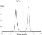
Fig. 3 illustrates a graph showing the phase shift performance of an LOE without the polarization scrambling coating. In this case, the LOE is made from of S-TIM8 glass (n ≈ 1.596) without coating 42 applied to the external surfaces. As shown, the phase shift is nearly constant for all wavelengths in the visible spectrum. This is undesirable, as will be described below. - Typically, the light entering the LOE is either from a RGB LED or white LED.
Fig. 4a illustrates a graph showing the high spectral peaks of RGB light, where the phase shift slope enhancements should preferably occur.Fig. 4b illustrates a graph showing the high spectral peaks of white light, where the phase shift slope enhancements should preferably occur. -
Fig. 5 illustrates a graph showing an example of the phase shift caused bypolarization scrambling coating 42 applied to a substrate in reference to the spectral peaks of a RGB LED light. In this case, thecoating 42 is comprised of TiO2, and was applied to asubstrate 34 made of S-TIM8 glass.Fig. 5 shows the results of two different thicknesses ofcoating 42, i.e. 300nm and 1000nm, respectively. As shown inFig. 5 , as the thickness of the layer is increased, the slope of the phase change in the visible wavelengths becomes larger. The spectral areas where the highest depolarization and slope should take place are indicated by dashed squares, and correspond to the spectral peaks of RGB LED. - As shown in
Fig. 5 , a small change in the wavelength of the light entering the LOE produces a large change in the phase shift. This is compared to the spectral range of the LED emission that illuminates the system. Thepolarization scrambling coating 42 causes different degrees of phase shift to parts of the narrow spectral peaks (at ≈480nm, ≈580nm and ≈640nm for the RGB LED, and ≈443nm for the white LED). Since the human eye integrates the intensity of the light of close wavelengths, this effect is comparable to viewing unpolarized light. The depolarization after the reflection is partial. Since the light is reflected by the external surfaces multiple times before being reflected by the facets 22, the accumulated depolarization of the light rays is relatively high. -
Fig. 6 illustrates a graph showing reflective properties of an exemplarypolarization scrambling coating 42 without anAR coating 44. In this case, coating 42 was applied at two different layer thicknesses, 300nm and 1000nm, respectively. As shown, coating 42 tends to be highly reflective (average of about 20% per side in the visible wavelengths), causing undesirable attenuation of the view of the outside world through the LOE. -
Fig. 7a illustrates a graph showing an example of a differential phase shift on reflection of light entering a LOE of the present invention. In this case, the substrate is coated with apolarization scrambling coating 42 comprised of a thick TiO2 layer, and anAR coating 44 on top of the polarization scrambling coating. The graph shows differential phase shift on reflection of light entering the LOE at angles of incidence of 55 degrees, in the visible wavelengths, for two different thicknesses ofcoating 42, i.e. 300nm and 1000nm, respectively. -
Fig. 7b illustrates a graph showing the phase shift on reflection using the same coatings as inFig. 7a , withcoating 42 applied in a thickness of 1000nm, for a variety of different angles in the TIR region. -
Fig. 8 illustrates reflections at normal incidence of a coating of consisting of layers of coating 42 (300nm and 1000nm TiO2 layer thicknesses) andcoating 44 as inFig. 7a at different wavelengths in the visible spectrum. As shown inFig. 8 , this coating performs as an AR coating at small angles, where it is apparent that the reflection is greatly reduced compared toFig. 6 (from about 18% average in the visible spectrum to about 4%). Using different designs and layer material this reflection can be reduced even lower. - It should be noted that the thickness of
coating 42 need not be identical for both external surfaces. Rather, different thicknesses ofcoating 42 could be applied to the different surfaces in in order to give each side of the LOE different slopes of phase change for any spectral region. For example if on one side the LOE has a small slope of phase change for a certain wavelength, the coating on the other side may randomly fall on a large slope of phase change, where the accumulated phase shift will be large. - Needless to say, if an incoming beam of light is polarized parallel or perpendicular to the facets 22, the
coating 42 will have no effect on the phase of the beam. - As stated above, the
polarization scrambling coating 42 can be applied to only a portion of one or both external surfaces, instead of the entire surface. - In some cases, it may be desirable for the LOE to be coated on one external surface, or a portion thereof, with a metallic coating. In that case, the
polarization scrambling coating 42 can be added between the substrate and the metallic layer, which will increase the phase shift change over the spectral region. -
Fig. 3 illustrates a graph showing an example of reflections of thepolarization scrambling coating 42 applied between the substrate and a metallic coating. The graph shows reflections of light at a 55° angle of incidence, at different wavelengths in the visible spectrum. The graph demonstrates the phase shift slopes without thepolarization scrambling coating 42, as well as withlayer 42 at different thicknesses, 300nm and 1000nm. - It should be noted that in some cases, the rays entering the LOE may not be in the same plane of the drawing, i.e. entering the LOE at another three dimensional angle. In this case even if the beam is polarized, it will not be polarized in reference to the TIR planes. Therefore, it will change the polarization state of the reflected beam and can be treated as unpolarized light.
-
Fig. 10 illustrates a display system having two LOEs, in which the beam is reflected from one LOE at an arbitrary angle to the second LOE. This reflection introduces a phase shift that will therefore change the polarization state of the beam so it will not be polarized upon reflection from the facets. Here again, thecoating 42 applied to the LOE surface will make sure that the reflection from the facets will not be dependent on the polarization state of the beam. -
Fig. 11 illustrates another embodiment of an LOE according to the present invention. In this embodiment, the LOE is designed for light beams to enter at the center of the waveguide and propagate towards each opposite end. In this case, the incoming beam travels through a converging lens 6. Rays 641, and 64R pass through the LOE. The beams to the eye will either be transmitted through the center facets, or will be reflected by the central facets and travel to the side and reflected towards the eye by the other facets. Traveling from the central facets to the side facets, the rays encounter TIR fromsurfaces surfaces - It should be appreciated that embodiments of the presently described LOE can be implemented in a large number of imaging applications, such as head-mounted displays (HMDs) and head-up displays (HUDs), cellular phones, compact displays, 3-D displays, compact beam expanders, as well as non-imaging applications, such as flat-panel indicators, compact illuminators and scanners.
- It is to be understood that the invention is not limited in its application to the details set forth in the description contained herein or illustrated in the drawings. The invention is capable of other embodiments and of being practiced and carried out in various ways. Hence, it is to be understood that the phraseology and terminology employed herein are for the purpose of description and should not be regarded as limiting. As such, those skilled in the art will appreciate that the conception upon which this disclosure is based may readily be utilized as a basis for designing other structures, methods, and systems for carrying out the several purposes of the presently disclosed subject matter.
Claims (7)
- A lightguide optical element (LOE) configured for polarization scrambling comprising:a transparent substrate (34) having a first refractive index, the substrate (34) comprising a pair of parallel external surfaces (26, 27) configured to propagate light within said LOE through total internal reflection (TIR), and a plurality of mutually parallel partially reflective internal surfaces (22), said plurality of mutually parallel partially reflective internal surfaces (22) being non-parallel to the pair of parallel external surfaces (26, 27) and configured to couple out said light to a viewer;a first coating (42) having a thickness between 100nm and 10 microns on at least one external surface (26, 27) of the substrate (34), the first coating (42) comprising a coating material having a second refractive index higher than said first refractive index; andan antireflective (AR) coating (44) on at least one external surface (26, 27) of the substrate (34) over said first coating (42);characterized in that the first coating (42) is configured to increase a phase shift between s-polarized and p-polarized components of light incident at angles of above TIR having a wavelength between 400nm and 1300nm.
- The LOE of claim 1, wherein said AR coating (44) is configured to reduce or eliminate reflections of light entering the LOE at angles of incidence between 0° and 50°.
- The LOE of claim 1, wherein said AR coating (44) is configured to reduce reflections of light entering the LOE at predetermined angles to between 0.3% and 10% reflected light.
- The LOE of claim 1, wherein said first coating (42) comprises a high index dielectric material.
- The LOE of claim 4, wherein said first coating (42) comprises a material selected from the group consisting of TiO2, Si3N4 and ZnS.
- The LOE of claim 1, wherein said AR coating (44) comprises one or more layers of at least one coating material selected from the group consisting of SiO2, HfO2, TiO2, MgF2 and Al2O3.
- The LOE of claim 1, wherein said AR coating (44) comprises one or more layers of at least one material having a refractive index in the range of 1.35 to 2.5.
Applications Claiming Priority (2)
| Application Number | Priority Date | Filing Date | Title |
|---|---|---|---|
| IL270991A IL270991B (en) | 2019-11-27 | 2019-11-27 | Lightguide optical element for polarization scrambling |
| PCT/IL2020/051166 WO2021105978A1 (en) | 2019-11-27 | 2020-11-10 | Lightguide optical element for polarization scrambling |
Publications (3)
| Publication Number | Publication Date |
|---|---|
| EP4066047A1 EP4066047A1 (en) | 2022-10-05 |
| EP4066047A4 EP4066047A4 (en) | 2023-01-04 |
| EP4066047B1 true EP4066047B1 (en) | 2025-01-08 |
Family
ID=72848747
Family Applications (1)
| Application Number | Title | Priority Date | Filing Date |
|---|---|---|---|
| EP20894867.9A Active EP4066047B1 (en) | 2019-11-27 | 2020-11-10 | Lightguide optical element for polarization scrambling |
Country Status (10)
| Country | Link |
|---|---|
| US (1) | US11573371B2 (en) |
| EP (1) | EP4066047B1 (en) |
| JP (1) | JP7511274B2 (en) |
| KR (1) | KR102772647B1 (en) |
| CN (1) | CN114467050B (en) |
| BR (1) | BR112022009871A2 (en) |
| CA (1) | CA3154682C (en) |
| IL (1) | IL270991B (en) |
| TW (1) | TWI836161B (en) |
| WO (1) | WO2021105978A1 (en) |
Families Citing this family (12)
| Publication number | Priority date | Publication date | Assignee | Title |
|---|---|---|---|---|
| IL237337B (en) | 2015-02-19 | 2020-03-31 | Amitai Yaakov | Compact head-mounted display system having uniform image |
| IL309806B2 (en) | 2018-09-09 | 2025-11-01 | Lumus Ltd | Optical systems that include light-guiding optical elements with two-dimensional expansion |
| TWM642752U (en) | 2018-11-08 | 2023-06-21 | 以色列商魯姆斯有限公司 | Light-guide display with reflector |
| WO2020095245A1 (en) | 2018-11-08 | 2020-05-14 | Lumus Ltd. | Optical Devices and Systems with Dichroic Beamsplitter Color Combiner |
| WO2020174433A1 (en) | 2019-02-28 | 2020-09-03 | Lumus Ltd. | Compact collimated image projector |
| JP7398131B2 (en) | 2019-03-12 | 2023-12-14 | ルムス エルティーディー. | image projector |
| WO2021105982A1 (en) | 2019-11-25 | 2021-06-03 | Lumus Ltd. | Method of polishing a surface of a waveguide |
| IL270991B (en) | 2019-11-27 | 2020-07-30 | Lumus Ltd | Lightguide optical element for polarization scrambling |
| EP4022380A4 (en) | 2019-12-05 | 2022-10-26 | Lumus Ltd. | Light-guide optical element employing complementary coated partial reflectors, and light-guide optical element having reduced light scattering |
| CN115004000A (en) | 2020-04-30 | 2022-09-02 | 鲁姆斯有限公司 | Optical sample characterization |
| CN218848473U (en) | 2020-05-12 | 2023-04-11 | 鲁姆斯有限公司 | Apparatus comprising projection optics and light guide |
| KR20230148324A (en) | 2021-03-01 | 2023-10-24 | 루머스 리미티드 | Optical system with compact coupling from projector to waveguide |
Family Cites Families (105)
| Publication number | Priority date | Publication date | Assignee | Title |
|---|---|---|---|---|
| CH563945A5 (en) | 1971-10-20 | 1975-07-15 | Balzers Patent Beteilig Ag | |
| US5270748A (en) | 1992-01-30 | 1993-12-14 | Mak Technologies, Inc. | High-speed eye tracking device and method |
| JP3219943B2 (en) | 1994-09-16 | 2001-10-15 | 株式会社東芝 | Planar direct-view display device |
| JPH08313843A (en) | 1995-05-16 | 1996-11-29 | Agency Of Ind Science & Technol | Wide-field-of-view high-resolution video presentation device using eye-tracking method |
| US6404550B1 (en) | 1996-07-25 | 2002-06-11 | Seiko Epson Corporation | Optical element suitable for projection display apparatus |
| GB2329901A (en) | 1997-09-30 | 1999-04-07 | Reckitt & Colman Inc | Acidic hard surface cleaning and disinfecting compositions |
| US6154321A (en) | 1998-01-20 | 2000-11-28 | University Of Washington | Virtual retinal display with eye tracking |
| US6231992B1 (en) | 1998-09-04 | 2001-05-15 | Yazaki Corporation | Partial reflector |
| US20050024849A1 (en) | 1999-02-23 | 2005-02-03 | Parker Jeffery R. | Methods of cutting or forming cavities in a substrate for use in making optical films, components or wave guides |
| US6671100B1 (en) | 1999-10-14 | 2003-12-30 | Stratos Product Development Llc | Virtual imaging system |
| AU6147201A (en) * | 2000-05-16 | 2001-11-26 | Du Pont | Aqueous dispersions for color imaging |
| ES2348532T3 (en) | 2000-06-05 | 2010-12-09 | Lumus Ltd | OPTICAL BEAM DILATOR GUIDED BY A SUBSTRATE. |
| IL136849A (en) | 2000-06-18 | 2004-09-27 | Beamus Ltd | Optical dynamic devices particularly for beam steering and optical communication |
| IL138895A (en) | 2000-10-05 | 2005-08-31 | Elop Electrooptics Ind Ltd | Optical switching devices |
| US6542307B2 (en) | 2000-10-20 | 2003-04-01 | Three-Five Systems, Inc. | Compact near-eye illumination system |
| EP1432948B1 (en) | 2001-09-26 | 2009-11-11 | Koninklijke Philips Electronics N.V. | Micro-structured illumination system for providing polarized light |
| IL148804A (en) | 2002-03-21 | 2007-02-11 | Yaacov Amitai | Optical device |
| EP1465047A1 (en) | 2003-04-03 | 2004-10-06 | Deutsche Thomson-Brandt Gmbh | Method for presenting menu buttons |
| IL157836A (en) | 2003-09-10 | 2009-08-03 | Yaakov Amitai | Optical devices particularly for remote viewing applications |
| IL157838A (en) | 2003-09-10 | 2013-05-30 | Yaakov Amitai | High brightness optical device |
| IL157837A (en) | 2003-09-10 | 2012-12-31 | Yaakov Amitai | Substrate-guided optical device particularly for three-dimensional displays |
| IL162573A (en) | 2004-06-17 | 2013-05-30 | Lumus Ltd | Substrate-guided optical device with very wide aperture |
| IL163361A (en) | 2004-08-05 | 2011-06-30 | Lumus Ltd | Optical device for light coupling into a guiding substrate |
| US7778508B2 (en) * | 2004-12-06 | 2010-08-17 | Nikon Corporation | Image display optical system, image display unit, illuminating optical system, and liquid crystal display unit |
| IL166799A (en) | 2005-02-10 | 2014-09-30 | Lumus Ltd | Substrate-guided optical device utilizing beam splitters |
| US10073264B2 (en) | 2007-08-03 | 2018-09-11 | Lumus Ltd. | Substrate-guide optical device |
| EP1849033B1 (en) | 2005-02-10 | 2019-06-19 | Lumus Ltd | Substrate-guided optical device utilizing thin transparent layer |
| US7751122B2 (en) | 2005-02-10 | 2010-07-06 | Lumus Ltd. | Substrate-guided optical device particularly for vision enhanced optical systems |
| EP1848966A1 (en) | 2005-02-17 | 2007-10-31 | Lumus Ltd | Personal navigation system |
| US8187481B1 (en) | 2005-05-05 | 2012-05-29 | Coho Holdings, Llc | Random texture anti-reflection optical surface treatment |
| US20070155277A1 (en) | 2005-07-25 | 2007-07-05 | Avi Amitai | Mobile/portable and personal pre-recorded sound effects electronic amplifier device/gadget |
| IL171820A (en) | 2005-11-08 | 2014-04-30 | Lumus Ltd | Polarizing optical device for light coupling |
| US10261321B2 (en) | 2005-11-08 | 2019-04-16 | Lumus Ltd. | Polarizing optical system |
| US7736006B2 (en) * | 2005-11-21 | 2010-06-15 | Microvision, Inc. | Substrate-guided display with improved image quality |
| US8360578B2 (en) | 2006-01-26 | 2013-01-29 | Nokia Corporation | Eye tracker device |
| IL173715A0 (en) | 2006-02-14 | 2007-03-08 | Lumus Ltd | Substrate-guided imaging lens |
| IL174170A (en) | 2006-03-08 | 2015-02-26 | Abraham Aharoni | Device and method for binocular alignment |
| IL177618A (en) | 2006-08-22 | 2015-02-26 | Lumus Ltd | Substrate- guided optical device |
| US20080151375A1 (en) | 2006-12-26 | 2008-06-26 | Ching-Bin Lin | Light guide means as dually effected by light concentrating and light diffusing |
| US8643948B2 (en) | 2007-04-22 | 2014-02-04 | Lumus Ltd. | Collimating optical device and system |
| IL183637A (en) | 2007-06-04 | 2013-06-27 | Zvi Lapidot | Distributed head-mounted display |
| JP2009128565A (en) | 2007-11-22 | 2009-06-11 | Toshiba Corp | Display device, display method, and head-up display |
| TW201115231A (en) | 2009-10-28 | 2011-05-01 | Coretronic Corp | Backlight module |
| US20120249797A1 (en) | 2010-02-28 | 2012-10-04 | Osterhout Group, Inc. | Head-worn adaptive display |
| KR101210163B1 (en) * | 2011-04-05 | 2012-12-07 | 엘지이노텍 주식회사 | Optical sheet and method of fabricating the same |
| JP5879973B2 (en) | 2011-11-30 | 2016-03-08 | ソニー株式会社 | Light reflecting member, light beam extending device, image display device, and optical device |
| US9297996B2 (en) | 2012-02-15 | 2016-03-29 | Microsoft Technology Licensing, Llc | Laser illumination scanning |
| US8665178B1 (en) | 2012-03-01 | 2014-03-04 | Google, Inc. | Partially-reflective waveguide stack and heads-up display using same |
| US9274338B2 (en) * | 2012-03-21 | 2016-03-01 | Microsoft Technology Licensing, Llc | Increasing field of view of reflective waveguide |
| WO2013167864A1 (en) | 2012-05-11 | 2013-11-14 | Milan Momcilo Popovich | Apparatus for eye tracking |
| IL219907A (en) | 2012-05-21 | 2017-08-31 | Lumus Ltd | Head-mounted display eyeball tracker integrated system |
| EP2854715A1 (en) | 2012-05-29 | 2015-04-08 | NLT Spine Ltd. | Laterally deflectable implant |
| US8909985B2 (en) | 2012-07-12 | 2014-12-09 | International Business Machines Corporation | Multiple hyperswap replication sessions |
| US10222535B2 (en) | 2013-07-02 | 2019-03-05 | 3M Innovative Properties Company | Flat light guide |
| WO2015012280A1 (en) | 2013-07-24 | 2015-01-29 | コニカミノルタ株式会社 | Sight line detection device |
| IL232197B (en) | 2014-04-23 | 2018-04-30 | Lumus Ltd | Compact head-mounted display system |
| IL235642B (en) | 2014-11-11 | 2021-08-31 | Lumus Ltd | Compact head-mounted display system protected by a hyperfine structure |
| IL236491B (en) | 2014-12-25 | 2020-11-30 | Lumus Ltd | A method for fabricating substrate-guided optical device |
| IL236490B (en) | 2014-12-25 | 2021-10-31 | Lumus Ltd | Optical component on a conductive substrate |
| IL237337B (en) | 2015-02-19 | 2020-03-31 | Amitai Yaakov | Compact head-mounted display system having uniform image |
| CN109073819A (en) * | 2016-04-07 | 2018-12-21 | 奇跃公司 | System and method for augmented reality |
| EP3458898B1 (en) | 2016-05-18 | 2023-02-15 | Lumus Ltd. | Head-mounted imaging device |
| US20170353714A1 (en) | 2016-06-06 | 2017-12-07 | Navid Poulad | Self-calibrating display system |
| CN108235739B (en) | 2016-10-09 | 2021-03-16 | 鲁姆斯有限公司 | Aperture Multiplier Using Rectangular Waveguide |
| MX386283B (en) | 2016-11-08 | 2025-03-18 | Lumus Ltd | Light-guide device with optical cutoff edge and corresponding production methods |
| EP3371642A4 (en) | 2016-12-02 | 2018-11-07 | Lumus Ltd. | Optical system with compact collimating image projector |
| CN108882845B (en) | 2016-12-31 | 2022-05-03 | 鲁姆斯有限公司 | Eye tracker based on retinal imaging via light-guide optical elements |
| EP3566092B1 (en) | 2017-01-04 | 2022-10-05 | Lumus Ltd. | Optical system for near-eye displays |
| KR102655450B1 (en) | 2017-02-22 | 2024-04-05 | 루머스 리미티드 | Light guide optical assembly |
| JP7300996B2 (en) | 2017-03-21 | 2023-06-30 | マジック リープ, インコーポレイテッド | Ocular imaging device using diffractive optical elements |
| KR20250070126A (en) | 2017-03-22 | 2025-05-20 | 루머스 리미티드 | Overlapping facets |
| IL251645B (en) * | 2017-04-06 | 2018-08-30 | Lumus Ltd | Light-guide optical element and method of its manufacture |
| WO2019016813A1 (en) | 2017-07-19 | 2019-01-24 | Lumus Ltd. | Lcos illumination via loe |
| CN111183393B (en) | 2017-09-29 | 2024-03-19 | 鲁姆斯有限公司 | Augmented reality display |
| WO2019077614A1 (en) | 2017-10-22 | 2019-04-25 | Lumus Ltd. | ENHANCED REALITY DEVICE MOUNTED ON THE HEAD AND USING AN OPTICAL BENCH |
| BR112020010057A2 (en) | 2017-11-21 | 2020-11-03 | Lumus Ltd. | optical device |
| WO2019106636A1 (en) | 2017-12-03 | 2019-06-06 | Lumus Ltd. | Optical device testing method and apparatus |
| IL274894B2 (en) | 2017-12-03 | 2024-04-01 | Lumus Ltd | Optical instrument alignment methods |
| US20190170327A1 (en) | 2017-12-03 | 2019-06-06 | Lumus Ltd. | Optical illuminator device |
| KR20200097289A (en) | 2017-12-10 | 2020-08-18 | 루머스 리미티드 | Image projector |
| KR20250138816A (en) * | 2017-12-10 | 2025-09-22 | 매직 립, 인코포레이티드 | Anti-reflective coatings on optical waveguides |
| CN113777783B (en) | 2018-01-02 | 2024-04-12 | 鲁姆斯有限公司 | Binocular augmented reality system with alignment correction and alignment correction method |
| US10551544B2 (en) | 2018-01-21 | 2020-02-04 | Lumus Ltd. | Light-guide optical element with multiple-axis internal aperture expansion |
| KR20250114148A (en) | 2018-04-08 | 2025-07-28 | 루머스 리미티드 | Optical sample characterization |
| US10830938B2 (en) | 2018-05-14 | 2020-11-10 | Lumus Ltd. | Projector configuration with subdivided optical aperture for near-eye displays, and corresponding optical systems |
| KR102750567B1 (en) | 2018-05-17 | 2025-01-06 | 루머스 리미티드 | Near-Eye Display with Overlapping Projector Assembly |
| IL259518B2 (en) | 2018-05-22 | 2023-04-01 | Lumus Ltd | Optical system and method for improvement of light field uniformity |
| EP3791224B1 (en) | 2018-05-23 | 2022-08-31 | Lumus Ltd. | Optical system including light-guide optical element with partially-reflective internal surfaces |
| CN210323582U (en) | 2018-05-27 | 2020-04-14 | 鲁姆斯有限公司 | Substrate-guided optical system with field curvature effect mitigation |
| IL279500B (en) | 2018-06-21 | 2022-09-01 | Lumus Ltd | Measurement technique for refractive index inhomogeneity between plates of a lightguide optical element (loe) |
| US11415812B2 (en) | 2018-06-26 | 2022-08-16 | Lumus Ltd. | Compact collimating optical device and system |
| JP7411255B2 (en) | 2018-07-16 | 2024-01-11 | ルムス エルティーディー. | Light-guiding optics employing polarized internal reflectors |
| TWI871876B (en) | 2018-08-26 | 2025-02-01 | 以色列商魯姆斯有限公司 | Near-eye displays |
| TWI827663B (en) | 2018-09-06 | 2024-01-01 | 以色列商魯姆斯有限公司 | Near-eye display with laser diode illumination |
| IL309806B2 (en) | 2018-09-09 | 2025-11-01 | Lumus Ltd | Optical systems that include light-guiding optical elements with two-dimensional expansion |
| TWM642752U (en) | 2018-11-08 | 2023-06-21 | 以色列商魯姆斯有限公司 | Light-guide display with reflector |
| WO2020095245A1 (en) | 2018-11-08 | 2020-05-14 | Lumus Ltd. | Optical Devices and Systems with Dichroic Beamsplitter Color Combiner |
| TWM598414U (en) | 2018-11-11 | 2020-07-11 | 以色列商魯姆斯有限公司 | Near eye display with intermediate window |
| EP3911983B1 (en) | 2019-01-15 | 2024-02-14 | Lumus Ltd. | Method of fabricating a symmetric light guide optical element |
| CN116300087B (en) | 2019-01-24 | 2026-07-28 | 鲁姆斯有限公司 | Optical system including LOE with three-stage expansion |
| JP7398131B2 (en) | 2019-03-12 | 2023-12-14 | ルムス エルティーディー. | image projector |
| CN118131484A (en) | 2019-05-06 | 2024-06-04 | 鲁姆斯有限公司 | Photoconductive optical element |
| KR20260023079A (en) | 2019-09-16 | 2026-02-20 | 루머스 리미티드 | Image display system with beam multiplication |
| IL270991B (en) | 2019-11-27 | 2020-07-30 | Lumus Ltd | Lightguide optical element for polarization scrambling |
| WO2021137228A1 (en) | 2019-12-30 | 2021-07-08 | Lumus Ltd. | Optical systems including light-guide optical elements with two-dimensional expansion |
-
2019
- 2019-11-27 IL IL270991A patent/IL270991B/en active IP Right Grant
-
2020
- 2020-11-10 US US17/312,443 patent/US11573371B2/en active Active
- 2020-11-10 KR KR1020227009210A patent/KR102772647B1/en active Active
- 2020-11-10 CA CA3154682A patent/CA3154682C/en active Active
- 2020-11-10 WO PCT/IL2020/051166 patent/WO2021105978A1/en not_active Ceased
- 2020-11-10 BR BR112022009871A patent/BR112022009871A2/en not_active Application Discontinuation
- 2020-11-10 EP EP20894867.9A patent/EP4066047B1/en active Active
- 2020-11-10 CN CN202080066045.2A patent/CN114467050B/en active Active
- 2020-11-10 JP JP2022526243A patent/JP7511274B2/en active Active
- 2020-11-25 TW TW109141410A patent/TWI836161B/en active
Also Published As
| Publication number | Publication date |
|---|---|
| WO2021105978A1 (en) | 2021-06-03 |
| JP2023503556A (en) | 2023-01-31 |
| CA3154682A1 (en) | 2021-06-03 |
| BR112022009871A2 (en) | 2022-08-09 |
| CA3154682C (en) | 2023-05-02 |
| CN114467050A (en) | 2022-05-10 |
| TWI836161B (en) | 2024-03-21 |
| IL270991B (en) | 2020-07-30 |
| TW202136853A (en) | 2021-10-01 |
| KR102772647B1 (en) | 2025-02-24 |
| EP4066047A1 (en) | 2022-10-05 |
| US11573371B2 (en) | 2023-02-07 |
| JP7511274B2 (en) | 2024-07-05 |
| KR20220050950A (en) | 2022-04-25 |
| EP4066047A4 (en) | 2023-01-04 |
| US20220019018A1 (en) | 2022-01-20 |
| CN114467050B (en) | 2025-03-14 |
Similar Documents
| Publication | Publication Date | Title |
|---|---|---|
| CA3154682C (en) | Lightguide optical element for polarization scrambling | |
| US20240219736A1 (en) | Highly efficient compact head-mounted display system having small input aperture | |
| CN108431640B (en) | Waveguide-based display with anti-reflective and highly reflective coating | |
| AU2004271392B2 (en) | Substrate-guided optical devices | |
| US12601919B2 (en) | Compact display system having uniform image | |
| KR102278463B1 (en) | Compact head mounted display system with uniform image | |
| JP6630678B2 (en) | Compact head-mounted display system | |
| CA2628871C (en) | Polarizing optical system | |
| CN116348707B (en) | Compact head-mounted display system with small input port and large output port | |
| CN114859560B (en) | Optical module and head-mounted display device | |
| CN114326123B (en) | Near-to-eye display device | |
| HK1232960A1 (en) | Compact head-mounted display system |
Legal Events
| Date | Code | Title | Description |
|---|---|---|---|
| STAA | Information on the status of an ep patent application or granted ep patent |
Free format text: STATUS: THE INTERNATIONAL PUBLICATION HAS BEEN MADE |
|
| PUAI | Public reference made under article 153(3) epc to a published international application that has entered the european phase |
Free format text: ORIGINAL CODE: 0009012 |
|
| STAA | Information on the status of an ep patent application or granted ep patent |
Free format text: STATUS: REQUEST FOR EXAMINATION WAS MADE |
|
| 17P | Request for examination filed |
Effective date: 20220329 |
|
| AK | Designated contracting states |
Kind code of ref document: A1 Designated state(s): AL AT BE BG CH CY CZ DE DK EE ES FI FR GB GR HR HU IE IS IT LI LT LU LV MC MK MT NL NO PL PT RO RS SE SI SK SM TR |
|
| A4 | Supplementary search report drawn up and despatched |
Effective date: 20221206 |
|
| RIC1 | Information provided on ipc code assigned before grant |
Ipc: G02B 27/01 20060101ALI20221130BHEP Ipc: G02B 27/00 20060101ALI20221130BHEP Ipc: G02B 6/10 20060101ALI20221130BHEP Ipc: G02F 1/01 20060101AFI20221130BHEP |
|
| DAV | Request for validation of the european patent (deleted) | ||
| DAX | Request for extension of the european patent (deleted) | ||
| P01 | Opt-out of the competence of the unified patent court (upc) registered |
Effective date: 20230527 |
|
| GRAP | Despatch of communication of intention to grant a patent |
Free format text: ORIGINAL CODE: EPIDOSNIGR1 |
|
| STAA | Information on the status of an ep patent application or granted ep patent |
Free format text: STATUS: GRANT OF PATENT IS INTENDED |
|
| INTG | Intention to grant announced |
Effective date: 20240809 |
|
| GRAS | Grant fee paid |
Free format text: ORIGINAL CODE: EPIDOSNIGR3 |
|
| GRAA | (expected) grant |
Free format text: ORIGINAL CODE: 0009210 |
|
| STAA | Information on the status of an ep patent application or granted ep patent |
Free format text: STATUS: THE PATENT HAS BEEN GRANTED |
|
| AK | Designated contracting states |
Kind code of ref document: B1 Designated state(s): AL AT BE BG CH CY CZ DE DK EE ES FI FR GB GR HR HU IE IS IT LI LT LU LV MC MK MT NL NO PL PT RO RS SE SI SK SM TR |
|
| REG | Reference to a national code |
Ref country code: GB Ref legal event code: FG4D |
|
| REG | Reference to a national code |
Ref country code: CH Ref legal event code: EP |
|
| REG | Reference to a national code |
Ref country code: DE Ref legal event code: R096 Ref document number: 602020044660 Country of ref document: DE |
|
| REG | Reference to a national code |
Ref country code: IE Ref legal event code: FG4D |
|
| REG | Reference to a national code |
Ref country code: LT Ref legal event code: MG9D |
|
| REG | Reference to a national code |
Ref country code: NL Ref legal event code: MP Effective date: 20250108 |
|
| REG | Reference to a national code |
Ref country code: AT Ref legal event code: MK05 Ref document number: 1758712 Country of ref document: AT Kind code of ref document: T Effective date: 20250108 |
|
| PG25 | Lapsed in a contracting state [announced via postgrant information from national office to epo] |
Ref country code: NL Free format text: LAPSE BECAUSE OF FAILURE TO SUBMIT A TRANSLATION OF THE DESCRIPTION OR TO PAY THE FEE WITHIN THE PRESCRIBED TIME-LIMIT Effective date: 20250108 |
|
| PG25 | Lapsed in a contracting state [announced via postgrant information from national office to epo] |
Ref country code: RS Free format text: LAPSE BECAUSE OF FAILURE TO SUBMIT A TRANSLATION OF THE DESCRIPTION OR TO PAY THE FEE WITHIN THE PRESCRIBED TIME-LIMIT Effective date: 20250408 |
|
| PG25 | Lapsed in a contracting state [announced via postgrant information from national office to epo] |
Ref country code: FI Free format text: LAPSE BECAUSE OF FAILURE TO SUBMIT A TRANSLATION OF THE DESCRIPTION OR TO PAY THE FEE WITHIN THE PRESCRIBED TIME-LIMIT Effective date: 20250108 |
|
| PG25 | Lapsed in a contracting state [announced via postgrant information from national office to epo] |
Ref country code: PL Free format text: LAPSE BECAUSE OF FAILURE TO SUBMIT A TRANSLATION OF THE DESCRIPTION OR TO PAY THE FEE WITHIN THE PRESCRIBED TIME-LIMIT Effective date: 20250108 |
|
| PG25 | Lapsed in a contracting state [announced via postgrant information from national office to epo] |
Ref country code: ES Free format text: LAPSE BECAUSE OF FAILURE TO SUBMIT A TRANSLATION OF THE DESCRIPTION OR TO PAY THE FEE WITHIN THE PRESCRIBED TIME-LIMIT Effective date: 20250108 |
|
| PG25 | Lapsed in a contracting state [announced via postgrant information from national office to epo] |
Ref country code: NO Free format text: LAPSE BECAUSE OF FAILURE TO SUBMIT A TRANSLATION OF THE DESCRIPTION OR TO PAY THE FEE WITHIN THE PRESCRIBED TIME-LIMIT Effective date: 20250408 Ref country code: IS Free format text: LAPSE BECAUSE OF FAILURE TO SUBMIT A TRANSLATION OF THE DESCRIPTION OR TO PAY THE FEE WITHIN THE PRESCRIBED TIME-LIMIT Effective date: 20250508 |
|
| PG25 | Lapsed in a contracting state [announced via postgrant information from national office to epo] |
Ref country code: HR Free format text: LAPSE BECAUSE OF FAILURE TO SUBMIT A TRANSLATION OF THE DESCRIPTION OR TO PAY THE FEE WITHIN THE PRESCRIBED TIME-LIMIT Effective date: 20250108 |
|
| PG25 | Lapsed in a contracting state [announced via postgrant information from national office to epo] |
Ref country code: PT Free format text: LAPSE BECAUSE OF FAILURE TO SUBMIT A TRANSLATION OF THE DESCRIPTION OR TO PAY THE FEE WITHIN THE PRESCRIBED TIME-LIMIT Effective date: 20250508 Ref country code: LV Free format text: LAPSE BECAUSE OF FAILURE TO SUBMIT A TRANSLATION OF THE DESCRIPTION OR TO PAY THE FEE WITHIN THE PRESCRIBED TIME-LIMIT Effective date: 20250108 |
|
| PG25 | Lapsed in a contracting state [announced via postgrant information from national office to epo] |
Ref country code: GR Free format text: LAPSE BECAUSE OF FAILURE TO SUBMIT A TRANSLATION OF THE DESCRIPTION OR TO PAY THE FEE WITHIN THE PRESCRIBED TIME-LIMIT Effective date: 20250409 Ref country code: BG Free format text: LAPSE BECAUSE OF FAILURE TO SUBMIT A TRANSLATION OF THE DESCRIPTION OR TO PAY THE FEE WITHIN THE PRESCRIBED TIME-LIMIT Effective date: 20250108 |
|
| PG25 | Lapsed in a contracting state [announced via postgrant information from national office to epo] |
Ref country code: AT Free format text: LAPSE BECAUSE OF FAILURE TO SUBMIT A TRANSLATION OF THE DESCRIPTION OR TO PAY THE FEE WITHIN THE PRESCRIBED TIME-LIMIT Effective date: 20250108 |
|
| PG25 | Lapsed in a contracting state [announced via postgrant information from national office to epo] |
Ref country code: SE Free format text: LAPSE BECAUSE OF FAILURE TO SUBMIT A TRANSLATION OF THE DESCRIPTION OR TO PAY THE FEE WITHIN THE PRESCRIBED TIME-LIMIT Effective date: 20250108 |
|
| PG25 | Lapsed in a contracting state [announced via postgrant information from national office to epo] |
Ref country code: SM Free format text: LAPSE BECAUSE OF FAILURE TO SUBMIT A TRANSLATION OF THE DESCRIPTION OR TO PAY THE FEE WITHIN THE PRESCRIBED TIME-LIMIT Effective date: 20250108 |
|
| REG | Reference to a national code |
Ref country code: DE Ref legal event code: R097 Ref document number: 602020044660 Country of ref document: DE |
|
| PG25 | Lapsed in a contracting state [announced via postgrant information from national office to epo] |
Ref country code: DK Free format text: LAPSE BECAUSE OF FAILURE TO SUBMIT A TRANSLATION OF THE DESCRIPTION OR TO PAY THE FEE WITHIN THE PRESCRIBED TIME-LIMIT Effective date: 20250108 |
|
| PG25 | Lapsed in a contracting state [announced via postgrant information from national office to epo] |
Ref country code: EE Free format text: LAPSE BECAUSE OF FAILURE TO SUBMIT A TRANSLATION OF THE DESCRIPTION OR TO PAY THE FEE WITHIN THE PRESCRIBED TIME-LIMIT Effective date: 20250108 Ref country code: CZ Free format text: LAPSE BECAUSE OF FAILURE TO SUBMIT A TRANSLATION OF THE DESCRIPTION OR TO PAY THE FEE WITHIN THE PRESCRIBED TIME-LIMIT Effective date: 20250108 |
|
| PG25 | Lapsed in a contracting state [announced via postgrant information from national office to epo] |
Ref country code: RO Free format text: LAPSE BECAUSE OF FAILURE TO SUBMIT A TRANSLATION OF THE DESCRIPTION OR TO PAY THE FEE WITHIN THE PRESCRIBED TIME-LIMIT Effective date: 20250108 |
|
| PG25 | Lapsed in a contracting state [announced via postgrant information from national office to epo] |
Ref country code: SK Free format text: LAPSE BECAUSE OF FAILURE TO SUBMIT A TRANSLATION OF THE DESCRIPTION OR TO PAY THE FEE WITHIN THE PRESCRIBED TIME-LIMIT Effective date: 20250108 |
|
| PLBE | No opposition filed within time limit |
Free format text: ORIGINAL CODE: 0009261 |
|
| STAA | Information on the status of an ep patent application or granted ep patent |
Free format text: STATUS: NO OPPOSITION FILED WITHIN TIME LIMIT |
|
| REG | Reference to a national code |
Ref country code: CH Ref legal event code: L10 Free format text: ST27 STATUS EVENT CODE: U-0-0-L10-L00 (AS PROVIDED BY THE NATIONAL OFFICE) Effective date: 20251119 |
|
| REG | Reference to a national code |
Ref country code: CH Ref legal event code: U11 Free format text: ST27 STATUS EVENT CODE: U-0-0-U10-U11 (AS PROVIDED BY THE NATIONAL OFFICE) Effective date: 20251201 |
|
| 26N | No opposition filed |
Effective date: 20251009 |
|
| PGFP | Annual fee paid to national office [announced via postgrant information from national office to epo] |
Ref country code: DE Payment date: 20251126 Year of fee payment: 6 |
|
| PGFP | Annual fee paid to national office [announced via postgrant information from national office to epo] |
Ref country code: GB Payment date: 20251125 Year of fee payment: 6 |
|
| PGFP | Annual fee paid to national office [announced via postgrant information from national office to epo] |
Ref country code: FR Payment date: 20251125 Year of fee payment: 6 |
|
| PGFP | Annual fee paid to national office [announced via postgrant information from national office to epo] |
Ref country code: CH Payment date: 20251201 Year of fee payment: 6 |
|
| PG25 | Lapsed in a contracting state [announced via postgrant information from national office to epo] |
Ref country code: IT Free format text: LAPSE BECAUSE OF FAILURE TO SUBMIT A TRANSLATION OF THE DESCRIPTION OR TO PAY THE FEE WITHIN THE PRESCRIBED TIME-LIMIT Effective date: 20250108 |
|
| PG25 | Lapsed in a contracting state [announced via postgrant information from national office to epo] |
Ref country code: LT Free format text: LAPSE BECAUSE OF FAILURE TO SUBMIT A TRANSLATION OF THE DESCRIPTION OR TO PAY THE FEE WITHIN THE PRESCRIBED TIME-LIMIT Effective date: 20250108 |
|
| PG25 | Lapsed in a contracting state [announced via postgrant information from national office to epo] |
Ref country code: MC Free format text: LAPSE BECAUSE OF FAILURE TO SUBMIT A TRANSLATION OF THE DESCRIPTION OR TO PAY THE FEE WITHIN THE PRESCRIBED TIME-LIMIT Effective date: 20250108 |
|
| PG25 | Lapsed in a contracting state [announced via postgrant information from national office to epo] |
Ref country code: LU Free format text: LAPSE BECAUSE OF NON-PAYMENT OF DUE FEES Effective date: 20251110 |