EP4064565A1 - Improved switch with hysteresis - Google Patents
Improved switch with hysteresis Download PDFInfo
- Publication number
- EP4064565A1 EP4064565A1 EP22163338.1A EP22163338A EP4064565A1 EP 4064565 A1 EP4064565 A1 EP 4064565A1 EP 22163338 A EP22163338 A EP 22163338A EP 4064565 A1 EP4064565 A1 EP 4064565A1
- Authority
- EP
- European Patent Office
- Prior art keywords
- transistor
- resistor
- base
- terminal
- emitter
- Prior art date
- Legal status (The legal status is an assumption and is not a legal conclusion. Google has not performed a legal analysis and makes no representation as to the accuracy of the status listed.)
- Withdrawn
Links
Images

Classifications
-
- H—ELECTRICITY
- H03—ELECTRONIC CIRCUITRY
- H03K—PULSE TECHNIQUE
- H03K17/00—Electronic switching or gating, i.e. not by contact-making and –breaking
- H03K17/51—Electronic switching or gating, i.e. not by contact-making and –breaking characterised by the components used
- H03K17/56—Electronic switching or gating, i.e. not by contact-making and –breaking characterised by the components used by the use, as active elements, of semiconductor devices
- H03K17/687—Electronic switching or gating, i.e. not by contact-making and –breaking characterised by the components used by the use, as active elements, of semiconductor devices the devices being field-effect transistors
- H03K17/693—Switching arrangements with several input- or output-terminals, e.g. multiplexers, distributors
-
- H—ELECTRICITY
- H03—ELECTRONIC CIRCUITRY
- H03K—PULSE TECHNIQUE
- H03K3/00—Circuits for generating electric pulses; Monostable, bistable or multistable circuits
- H03K3/02—Generators characterised by the type of circuit or by the means used for producing pulses
- H03K3/26—Generators characterised by the type of circuit or by the means used for producing pulses by the use, as active elements, of bipolar transistors with internal or external positive feedback
- H03K3/28—Generators characterised by the type of circuit or by the means used for producing pulses by the use, as active elements, of bipolar transistors with internal or external positive feedback using means other than a transformer for feedback
- H03K3/281—Generators characterised by the type of circuit or by the means used for producing pulses by the use, as active elements, of bipolar transistors with internal or external positive feedback using means other than a transformer for feedback using at least two transistors so coupled that the input of one is derived from the output of another, e.g. multivibrator
- H03K3/286—Generators characterised by the type of circuit or by the means used for producing pulses by the use, as active elements, of bipolar transistors with internal or external positive feedback using means other than a transformer for feedback using at least two transistors so coupled that the input of one is derived from the output of another, e.g. multivibrator bistable
- H03K3/2893—Bistables with hysteresis, e.g. Schmitt trigger
-
- H—ELECTRICITY
- H03—ELECTRONIC CIRCUITRY
- H03K—PULSE TECHNIQUE
- H03K17/00—Electronic switching or gating, i.e. not by contact-making and –breaking
- H03K17/16—Modifications for eliminating interference voltages or currents
-
- H—ELECTRICITY
- H03—ELECTRONIC CIRCUITRY
- H03K—PULSE TECHNIQUE
- H03K17/00—Electronic switching or gating, i.e. not by contact-making and –breaking
- H03K17/30—Modifications for providing a predetermined threshold before switching
-
- H—ELECTRICITY
- H03—ELECTRONIC CIRCUITRY
- H03K—PULSE TECHNIQUE
- H03K17/00—Electronic switching or gating, i.e. not by contact-making and –breaking
- H03K17/51—Electronic switching or gating, i.e. not by contact-making and –breaking characterised by the components used
- H03K17/56—Electronic switching or gating, i.e. not by contact-making and –breaking characterised by the components used by the use, as active elements, of semiconductor devices
- H03K17/60—Electronic switching or gating, i.e. not by contact-making and –breaking characterised by the components used by the use, as active elements, of semiconductor devices the devices being bipolar transistors
-
- H—ELECTRICITY
- H03—ELECTRONIC CIRCUITRY
- H03K—PULSE TECHNIQUE
- H03K19/00—Logic circuits, i.e. having at least two inputs acting on one output; Inverting circuits
- H03K19/003—Modifications for increasing the reliability for protection
- H03K19/00369—Modifications for compensating variations of temperature, supply voltage or other physical parameters
- H03K19/00376—Modifications for compensating variations of temperature, supply voltage or other physical parameters in bipolar transistor circuits
-
- H—ELECTRICITY
- H10—SEMICONDUCTOR DEVICES; ELECTRIC SOLID-STATE DEVICES NOT OTHERWISE PROVIDED FOR
- H10D—INORGANIC ELECTRIC SEMICONDUCTOR DEVICES
- H10D84/00—Integrated devices formed in or on semiconductor substrates that comprise only semiconducting layers, e.g. on Si wafers or on GaAs-on-Si wafers
- H10D84/60—Integrated devices formed in or on semiconductor substrates that comprise only semiconducting layers, e.g. on Si wafers or on GaAs-on-Si wafers characterised by the integration of at least one component covered by groups H10D10/00 or H10D18/00, e.g. integration of BJTs
- H10D84/645—Combinations of only lateral BJTs
-
- H—ELECTRICITY
- H03—ELECTRONIC CIRCUITRY
- H03K—PULSE TECHNIQUE
- H03K2217/00—Indexing scheme related to electronic switching or gating, i.e. not by contact-making or -breaking covered by H03K17/00
- H03K2217/0072—Low side switches, i.e. the lower potential [DC] or neutral wire [AC] being directly connected to the switch and not via the load
Definitions
- This relates to solid state switches and switch circuits and simple switches/switch circuits which include Bipolar Junction Transistors (BJTs).
- BJTs Bipolar Junction Transistors
- a single BJT switch has no hysteresis.
- An unstable input voltage e.g. with noise
- the switch may turn on and off repeatedly.
- Switch circuitry comprising an input terminal, said input terminal connected to the base of of a first transistor (Q1) via a first resistor R3, said first transistor being an NPN Bipolar Gate Transistor (Q1), further comprising a second resistor (R5) connected between the base of said first transistor Q1 and ground, and including an output line or terminal connected to the collector of said first transistor (Q1), and wherein the emitter of said first transistor (Q1) is connected to ground (earth), said circuitry further including a second transistor (Q2) , said second transistor being a PNP Bipolar Gate Transistor, wherein the collector of said second transistor (Q2) is connected via a third resistor (R8) to the base of said first transistor (Q1), and the emitter of said second transistor Q2 is connected to said input terminal, and wherein the emitter of said second transistor ( Q2) is additionally connected to the base of said second transistor Q2 via a fourth resistor R11; and the base of said second transistor (Q2) being additionally connected to the output terminal (3) via a fifth resist
- Said diode D1 may be electrically connected between said fourth resistor (R10) and output line/terminal (3).
- Fig 1 shows a known simple switch arrangement with input line 1 or terminal (e.g. from a switching source 2) connected via resistor R3 to the base of BJT (NPN) designated Q1. There is included resistor R5 between the base and ground. The output line/terminal 3 is shown, effectively connected to the collector of Q1.
- NPN BJT
- R3 is used to limit the current to base and R5 to ensure Q1 is off when there is no voltage at the input.
- this circuit has no hysteresis so in a typical open collector NPN switch below there is no Schmitt trigger or hysteresis. Noise on the input can toggle the switch on and off means it can be unstable.
- a known solution is to use add a comparator for to add hysteresis.
- Fig 2 shows such an arrangement.
- the comparator 4 needs another power supply as the comparator needs regulated voltage.
- the circuitry provides a switch with hysteresis which is efficient and reliable.
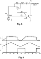
- Figure 3 shows an example. As with figure 1 there is an input line or terminal 1 (e.g. electrically connected or connectable to a switching source 2) which is connected via resistor R3 to the base of a BJT (NPN) designated Q1. There is included in the circuitry resistor R5, connected between the base of Q1 and ground. The output line or terminal 3 is shown, effectively connected to the collector of Q1, and can be considered an open collector output. The emitter of Q1 is directly connected to ground (earth).
- the circuit includes a further BJT designated Q2 which is a PNP transistor.
- the collector of Q2 is connected via a resistor R8 to the base of Q1, and the emitter of Q2 is connected to the input line/terminal 1.
- the emitter of Q2 is also connected to the base of Q2 via resistor R11; the base of Q2 also being connected to the output terminal via a resistor R10 and a diode D1; diode D1 being located between resistor R10 and output line/terminal 3.
- the positions of the resistor R10 and diode may be interchanged ie.
- the resistor R10 may be located (i.e. electrically connected between the diode and terminal 3.
- the circuitry effectively provides a Schmitt trigger switch by adding a second BJT Q2 which is a PNP BJT, as well as resistors R8, R11, R10 and a diode.
- Input voltage rises to threshold voltage just enough to turn on Q1 through R3.
- Q1 turns on, it will also turn on Q2 through R10 and diode.
- Q2 turns on, more current is provided to the base of Q1 through R8. This forces the Q1 to "turn on” state. This enhances the turn on current to base of Q1.
- Figure 4 shows an example of operation of the circuitry of figure 3 .
- the set-up is as follows; i) Input toggling on/off with a slow ramp up and down ii) a DC voltage source though a resistor is connected to the Open Collector Output 3.
- Plots A, B, C show the voltage at points A, B, C respectively in figure 3 .
- the Q1 NPN base voltage shoots up from 0.5V to 0.7V. This is a result of Q2 providing more current to the base.
- the turn on voltage low to high
- the turn off voltage high to low
- Threshold voltage and hysteresis range can be adjusted by adjusting the resistance values (of which resistors).
Landscapes
- Engineering & Computer Science (AREA)
- Power Engineering (AREA)
- Physics & Mathematics (AREA)
- Computer Hardware Design (AREA)
- Computing Systems (AREA)
- General Engineering & Computer Science (AREA)
- Mathematical Physics (AREA)
- Manipulation Of Pulses (AREA)
- Electronic Switches (AREA)
- Measurement Of Current Or Voltage (AREA)
- Switches That Are Operated By Magnetic Or Electric Fields (AREA)
Abstract
Description
- This relates to solid state switches and switch circuits and simple switches/switch circuits which include Bipolar Junction Transistors (BJTs).
- A single BJT switch has no hysteresis. An unstable input voltage (e.g. with noise) at or close to the threshold level to the base may cause the switch to turn on and off repeatedly.
- More complex designs available with multiple BJTs (three or more BJT's) or with comparator solution are used to overcome this problem and to create hysteresis.
- It is an object of the invention to overcome this problem and to create a simpler and cheaper switch circuit which includes hysteresis.
- The problem of a single BJT NPN open collector switch without hysteresis is vulnerable to unstable input voltage at threshold level to the base of the BJT is solved by adding another BJT (PNP) switch to enhance the turn on current to the base of the NPN.
- In one aspect is provided Switch circuitry comprising an input terminal, said input terminal connected to the base of of a first transistor (Q1) via a first resistor R3, said first transistor being an NPN Bipolar Gate Transistor (Q1), further comprising a second resistor (R5) connected between the base of said first transistor Q1 and ground, and including an output line or terminal connected to the collector of said first transistor (Q1), and wherein the emitter of said first transistor (Q1) is connected to ground (earth), said circuitry further including a second transistor (Q2) , said second transistor being a PNP Bipolar Gate Transistor, wherein the collector of said second transistor (Q2) is connected via a third resistor (R8) to the base of said first transistor (Q1), and the emitter of said second transistor Q2 is connected to said input terminal, and wherein the emitter of said second transistor ( Q2) is additionally connected to the base of said second transistor Q2 via a fourth resistor R11; and the base of said second transistor (Q2) being additionally connected to the output terminal (3) via a fifth resistor (R10) and a diode (D1.
- Said diode D1 may be electrically connected between said fourth resistor (R10) and output line/terminal (3).
- The present invention is now described by way of example with reference to the accompanying drawings in which:
-
Figure 1 shows a known simple switch arrangement; -
Figure 2 shows a known switch arrangement with a comparator; -
Figure 3 shows an example of the invention; -
Figure 4 shows operation of the circuitry offigure 3 ; -
Fig 1 shows a known simple switch arrangement withinput line 1 or terminal (e.g. from a switching source 2) connected via resistor R3 to the base of BJT
(NPN) designated Q1. There is included resistor R5 between the base and ground. The output line/terminal 3 is shown, effectively connected to the collector of Q1. Thus, this describes a conventional open collector NPN BJT switch with BJT Q1. R3 is used to limit the current to base and R5 to ensure Q1 is off when there is no voltage at the input. - As mentioned, this circuit has no hysteresis so in a typical open collector NPN switch below there is no Schmitt trigger or hysteresis. Noise on the input can toggle the switch on and off means it can be unstable.
- A known solution is to use add a comparator for to add hysteresis.
Fig 2 shows such an arrangement. In addition, thecomparator 4 needs another power supply as the comparator needs regulated voltage. These additional requirements/components mean the circuitry is more complicated and expensive. - In one example, the circuitry provides a switch with hysteresis which is efficient and reliable.
Figure 3 shows an example. As withfigure 1 there is an input line or terminal 1 (e.g. electrically connected or connectable to a switching source 2) which is connected via resistor R3 to the base of a BJT (NPN) designated Q1. There is included in the circuitry resistor R5, connected between the base of Q1 and ground. The output line orterminal 3 is shown, effectively connected to the collector of Q1, and can be considered an open collector output. The emitter of Q1 is directly connected to ground (earth). - In addition, the circuit includes a further BJT designated Q2 which is a PNP transistor. The collector of Q2 is connected via a resistor R8 to the base of Q1, and the emitter of Q2 is connected to the input line/
terminal 1. The emitter of Q2 is also connected to the base of Q2 via resistor R11; the base of Q2 also being connected to the output terminal via a resistor R10 and a diode D1; diode D1 being located between resistor R10 and output line/terminal 3. Optionally the positions of the resistor R10 and diode may be interchanged ie. The resistor R10 may be located (i.e. electrically connected between the diode andterminal 3. - So, the circuitry effectively provides a Schmitt trigger switch by adding a second BJT Q2 which is a PNP BJT, as well as resistors R8, R11, R10 and a diode.
- Input voltage rises to threshold voltage just enough to turn on Q1 through R3. When Q1 turns on, it will also turn on Q2 through R10 and diode. When Q2 turns on, more current is provided to the base of Q1 through R8. This forces the Q1 to "turn on" state. This enhances the turn on current to base of Q1.
-
Figure 4 shows an example of operation of the circuitry offigure 3 . The set-up is as follows; i) Input toggling on/off with a slow ramp up and down ii) a DC voltage source though a resistor is connected to theOpen Collector Output 3. Plots A, B, C show the voltage at points A, B, C respectively infigure 3 . - As Q1 NPN turns on (output voltage go to zero), the Q1 NPN base voltage shoots up from 0.5V to 0.7V. This is a result of Q2 providing more current to the base. In this example, the turn on voltage (low to high) is 6.2V and the turn off voltage (high to low) is 2.8V. Threshold voltage and hysteresis range can be adjusted by adjusting the resistance values (of which resistors).
Claims (2)
- Switch circuitry comprising an input terminal (1), said input terminal connected to the base of of a first transistor (Q1) via a first resistor R3, said first transistor being an NPN Bipolar Gate Transistor (Q1), further comprising a second resistor (R5) connected between the base of said first transistor Q1 and ground, and including an output line or terminal (3) connected to the collector of said first transistor (Q1), and wherein the emitter of said first transistor (Q1) is connected to ground (earth), said circuitry further including a second transistor (Q2) , said second transistor being a PNP Bipolar Gate Transistor, wherein the collector of said second transistor (Q2) is connected via a third resistor (R8) to the base of said first transistor (Q1), and the emitter of said second transistor Q2 is connected to said input terminal (1), and wherein the emitter of said second transistor ( Q2) is additionally connected to the base of said second transistor Q2 via a fourth resistor R11; and the base of said second transistor (Q2) being additionally connected to the output terminal (3) via a fifth resistor (R10) and a diode (D1.
- Circuitry as claimed in claim 1 wherein said diode D1 is electrically connected between said fourth resistor (R10) and output line/terminal (3).
Applications Claiming Priority (1)
| Application Number | Priority Date | Filing Date | Title |
|---|---|---|---|
| SG10202102992W | 2021-03-23 |
Publications (1)
| Publication Number | Publication Date |
|---|---|
| EP4064565A1 true EP4064565A1 (en) | 2022-09-28 |
Family
ID=80928942
Family Applications (1)
| Application Number | Title | Priority Date | Filing Date |
|---|---|---|---|
| EP22163338.1A Withdrawn EP4064565A1 (en) | 2021-03-23 | 2022-03-21 | Improved switch with hysteresis |
Country Status (4)
| Country | Link |
|---|---|
| US (1) | US11575379B2 (en) |
| EP (1) | EP4064565A1 (en) |
| KR (1) | KR102640530B1 (en) |
| CN (1) | CN115118260B (en) |
Citations (3)
| Publication number | Priority date | Publication date | Assignee | Title |
|---|---|---|---|---|
| US5287014A (en) * | 1990-05-25 | 1994-02-15 | Kabushiki Kaisha Toshiba | Hysteresis circuit |
| US20030193339A1 (en) * | 2002-04-11 | 2003-10-16 | Philippart Timothy P. | Circuit for monitoring an open collector output circuit with a significant offset |
| DE102018217496A1 (en) * | 2018-02-20 | 2019-08-22 | Mitsubishi Electric Corporation | START CIRCUIT |
Family Cites Families (7)
| Publication number | Priority date | Publication date | Assignee | Title |
|---|---|---|---|---|
| JPS62171216A (en) | 1986-01-22 | 1987-07-28 | Nec Corp | Semiconductor logic circuit |
| GB2221088B (en) | 1988-07-22 | 1992-02-26 | Texas Instruments Ltd | A semiconductor switching device |
| KR0154775B1 (en) * | 1995-12-20 | 1998-12-15 | 김광호 | Output Protection Circuit with Hysteresis |
| KR101103750B1 (en) | 2010-03-31 | 2012-01-06 | 국민대학교산학협력단 | Electronic switch with hysteresis characteristics |
| JP6083429B2 (en) * | 2014-12-24 | 2017-02-22 | オンキヨー株式会社 | Mute control circuit |
| US20160241231A1 (en) * | 2015-02-17 | 2016-08-18 | Infineon Technologies Ag | RF Switch |
| CN109936349B (en) * | 2019-03-29 | 2024-06-28 | 吕建华 | A method for improving the switching speed of power electronic switch chip and its application |
-
2022
- 2022-01-20 US US17/648,492 patent/US11575379B2/en active Active
- 2022-02-18 KR KR1020220021618A patent/KR102640530B1/en active Active
- 2022-02-18 CN CN202210150675.9A patent/CN115118260B/en active Active
- 2022-03-21 EP EP22163338.1A patent/EP4064565A1/en not_active Withdrawn
Patent Citations (3)
| Publication number | Priority date | Publication date | Assignee | Title |
|---|---|---|---|---|
| US5287014A (en) * | 1990-05-25 | 1994-02-15 | Kabushiki Kaisha Toshiba | Hysteresis circuit |
| US20030193339A1 (en) * | 2002-04-11 | 2003-10-16 | Philippart Timothy P. | Circuit for monitoring an open collector output circuit with a significant offset |
| DE102018217496A1 (en) * | 2018-02-20 | 2019-08-22 | Mitsubishi Electric Corporation | START CIRCUIT |
Also Published As
| Publication number | Publication date |
|---|---|
| KR20220132422A (en) | 2022-09-30 |
| CN115118260B (en) | 2026-05-12 |
| KR102640530B1 (en) | 2024-02-27 |
| US20220311438A1 (en) | 2022-09-29 |
| US11575379B2 (en) | 2023-02-07 |
| CN115118260A (en) | 2022-09-27 |
Similar Documents
| Publication | Publication Date | Title |
|---|---|---|
| US20010017537A1 (en) | Voltage regulator provided with a current limiter | |
| JPH02220114A (en) | voltage stabilizer | |
| US4539492A (en) | Darlington transistor circuit | |
| US6570437B2 (en) | Bandgap reference voltage circuit | |
| US11575379B2 (en) | Switch with hysteresis | |
| JPH0121703B2 (en) | ||
| US20030048008A1 (en) | Current-limiting logic interface circuit | |
| US7288857B2 (en) | Self-latching power supply apparatus | |
| EP0168419A1 (en) | Zener referenced threshold detector with hysteresis | |
| US5764088A (en) | Control circuit for an electronic switch, and a switch constituting an application thereof | |
| CN219247818U (en) | A PWM signal output protection circuit and intelligent ignition coil drive | |
| US5914628A (en) | Circuit for controlling a triac at the voltage zero | |
| CN112327985B (en) | Low dropout linear voltage stabilizing circuit, low dropout linear voltage stabilizer and electronic chip | |
| KR940002861B1 (en) | Hysteresis circuit | |
| US4467226A (en) | Darlington complementary circuit for preventing zero crossover distortion | |
| US6154063A (en) | Class AB emitter follower buffers | |
| CN212435354U (en) | Small current output current limiting protection circuit | |
| US9946280B2 (en) | Current output stage having automatic active-passive switching | |
| US4810962A (en) | Voltage regulator capable of sinking current | |
| JP2622142B2 (en) | Current comparison circuit | |
| JPS5928936B2 (en) | Photoelectric switch | |
| SU1619241A2 (en) | D.c. voltage stabilizer | |
| JP2905671B2 (en) | Stabilized power supply circuit | |
| SU1274149A1 (en) | Versions of transistor-transistor logic element | |
| KR940007703Y1 (en) | TV vertical deflection bias circuit |
Legal Events
| Date | Code | Title | Description |
|---|---|---|---|
| PUAI | Public reference made under article 153(3) epc to a published international application that has entered the european phase |
Free format text: ORIGINAL CODE: 0009012 |
|
| STAA | Information on the status of an ep patent application or granted ep patent |
Free format text: STATUS: THE APPLICATION HAS BEEN PUBLISHED |
|
| AK | Designated contracting states |
Kind code of ref document: A1 Designated state(s): AL AT BE BG CH CY CZ DE DK EE ES FI FR GB GR HR HU IE IS IT LI LT LU LV MC MK MT NL NO PL PT RO RS SE SI SK SM TR |
|
| STAA | Information on the status of an ep patent application or granted ep patent |
Free format text: STATUS: REQUEST FOR EXAMINATION WAS MADE |
|
| 17P | Request for examination filed |
Effective date: 20230309 |
|
| RBV | Designated contracting states (corrected) |
Designated state(s): AL AT BE BG CH CY CZ DE DK EE ES FI FR GB GR HR HU IE IS IT LI LT LU LV MC MK MT NL NO PL PT RO RS SE SI SK SM TR |
|
| P01 | Opt-out of the competence of the unified patent court (upc) registered |
Effective date: 20230327 |
|
| RAP1 | Party data changed (applicant data changed or rights of an application transferred) |
Owner name: BORGWARNER US TECHNOLOGIES LLC |
|
| STAA | Information on the status of an ep patent application or granted ep patent |
Free format text: STATUS: THE APPLICATION HAS BEEN WITHDRAWN |
|
| 18W | Application withdrawn |
Effective date: 20250409 |