EP4064557A1 - Doherty amplifier and communication device - Google Patents
Doherty amplifier and communication device Download PDFInfo
- Publication number
- EP4064557A1 EP4064557A1 EP19955647.3A EP19955647A EP4064557A1 EP 4064557 A1 EP4064557 A1 EP 4064557A1 EP 19955647 A EP19955647 A EP 19955647A EP 4064557 A1 EP4064557 A1 EP 4064557A1
- Authority
- EP
- European Patent Office
- Prior art keywords
- amplifier
- signal
- input
- peak amplifier
- transmission line
- Prior art date
- Legal status (The legal status is an assumption and is not a legal conclusion. Google has not performed a legal analysis and makes no representation as to the accuracy of the status listed.)
- Granted
Links
Images




Classifications
-
- H—ELECTRICITY
- H03—ELECTRONIC CIRCUITRY
- H03F—AMPLIFIERS
- H03F1/00—Details of amplifiers with only discharge tubes, only semiconductor devices or only unspecified devices as amplifying elements
- H03F1/02—Modifications of amplifiers to raise the efficiency, e.g. gliding Class A stages, use of an auxiliary oscillation
- H03F1/0205—Modifications of amplifiers to raise the efficiency, e.g. gliding Class A stages, use of an auxiliary oscillation in transistor amplifiers
- H03F1/0288—Modifications of amplifiers to raise the efficiency, e.g. gliding Class A stages, use of an auxiliary oscillation in transistor amplifiers using a main and one or several auxiliary peaking amplifiers whereby the load is connected to the main amplifier using an impedance inverter, e.g. Doherty amplifiers
-
- H—ELECTRICITY
- H03—ELECTRONIC CIRCUITRY
- H03F—AMPLIFIERS
- H03F1/00—Details of amplifiers with only discharge tubes, only semiconductor devices or only unspecified devices as amplifying elements
- H03F1/56—Modifications of input or output impedances, not otherwise provided for
-
- H—ELECTRICITY
- H03—ELECTRONIC CIRCUITRY
- H03F—AMPLIFIERS
- H03F3/00—Amplifiers with only discharge tubes or only semiconductor devices as amplifying elements
- H03F3/20—Power amplifiers, e.g. Class B amplifiers, Class C amplifiers
- H03F3/21—Power amplifiers, e.g. Class B amplifiers, Class C amplifiers with semiconductor devices only
- H03F3/211—Power amplifiers, e.g. Class B amplifiers, Class C amplifiers with semiconductor devices only using a combination of several amplifiers
-
- H—ELECTRICITY
- H03—ELECTRONIC CIRCUITRY
- H03F—AMPLIFIERS
- H03F3/00—Amplifiers with only discharge tubes or only semiconductor devices as amplifying elements
- H03F3/60—Amplifiers in which coupling networks have distributed constants, e.g. with waveguide resonators
- H03F3/602—Combinations of several amplifiers
-
- H—ELECTRICITY
- H01—ELECTRIC ELEMENTS
- H01P—WAVEGUIDES; RESONATORS, LINES, OR OTHER DEVICES OF THE WAVEGUIDE TYPE
- H01P5/00—Coupling devices of the waveguide type
- H01P5/12—Coupling devices having more than two ports
- H01P5/16—Conjugate devices, i.e. devices having at least one port decoupled from one other port
-
- H—ELECTRICITY
- H03—ELECTRONIC CIRCUITRY
- H03F—AMPLIFIERS
- H03F2200/00—Indexing scheme relating to amplifiers
- H03F2200/423—Amplifier output adaptation especially for transmission line coupling purposes, e.g. impedance adaptation
-
- H—ELECTRICITY
- H03—ELECTRONIC CIRCUITRY
- H03F—AMPLIFIERS
- H03F2200/00—Indexing scheme relating to amplifiers
- H03F2200/451—Indexing scheme relating to amplifiers the amplifier being a radio frequency amplifier
Definitions
- the present disclosure relates to a Doherty amplifier and a communication device.
- Patent Literature 1 discloses a Doherty amplifier including an isolation resistance variable divider that divides an input signal into two and outputs the two divided signals, a carrier amplifier circuit that amplifies one of the two signals output from the isolation resistance variable divider, and a peak amplifier circuit that amplifies the other of the two signals.
- the Doherty amplifier also includes a detection circuit that converts power of an input signal into a voltage and outputs the voltage as an input power level, and a control circuit that varies a division ratio of an input signal in the isolation resistance variable divider by controlling a resistance value of a variable resistor included in the isolation resistance variable divider according to the input power level output from the detection circuit.
- the Doherty amplifier can prevent a decrease in gain of the amplified signal due to a division loss in the isolation resistance variable divider. That is, the Doherty amplifier can prevent a decrease in gain of a combined signal of the signal output from the carrier amplifier circuit and the signal output from the peak amplifier circuit during a period from a backoff to a saturation operation.
- the Doherty amplifier includes a delay circuit that delays the input signal by a time required from when the input signal is input to the detection circuit to when the control circuit finishes varying the division ratio.
- Patent Literature 1 JP 2008-125044 A
- the Doherty amplifier disclosed in Patent Literature 1 includes a delay circuit that delays an input signal. Therefore, this Doherty amplifier has a problem that the Doherty amplifier cannot output the amplified signal until the delay time of the delay circuit elapses after the input signal is input to the delay circuit.
- the present disclosure has been accomplished to solve the above problems, and an object of the present disclosure is to obtain a Doherty amplifier capable of preventing a decrease in gain of a combined signal of a signal output from a carrier amplifier and a signal output from a peak amplifier during a period from a backoff to a saturation operation without having a delay circuit that delays a signal to be amplified.
- the Doherty amplifier includes: a first transmission line having a first end connected to an input terminal to which a signal to be amplified is input; a second transmission line having a first end connected to the input terminal; a resistor connected between a second end of the first transmission line and a second end of the second transmission line; a carrier amplifier to amplify a signal output from the second end of the first transmission line and output the amplified signal to an output combining point; and a peak amplifier to amplify a signal output from the second end of the second transmission line and output the amplified signal to the output combining point, wherein a ratio of a characteristic impedance of the second transmission line to a characteristic impedance of the first transmission line is a power division ratio of the signal to be amplified between the carrier amplifier and the peak amplifier when both of the carrier amplifier and the peak amplifier are saturated, and a resistance value of the resistor is a value obtained by multiplying, by a proportionality coefficient that is equal to or greater than 0 but less
- the Doherty amplifier is configured in such a manner that: the ratio of the characteristic impedance of the second transmission line to the characteristic impedance of the first transmission line is a power division ratio of the signal to be amplified between the carrier amplifier and the peak amplifier when both of the carrier amplifier and the peak amplifier are saturated; and a resistance value of the resistor is a value obtained by multiplying, by a proportionality coefficient that is equal to or greater than 0 but less than 1, a sum of the input impedance of the carrier amplifier when the carrier amplifier reaches saturation and the input impedance of the peak amplifier when the peak amplifier reaches saturation.
- the Doherty amplifier according to the present disclosure can prevent a decrease in gain of a combined signal of a signal output from the carrier amplifier and a signal output from the peak amplifier during a period from a backoff to a saturation operation without having a delay circuit that delays the signal to be amplified.
- FIG. 1 is a configuration diagram illustrating a Doherty amplifier 10 according to a first embodiment.
- an input terminal 1 is a terminal for receiving a signal to be amplified from the outside of the Doherty amplifier 10.
- a load 2 is an external load of the Doherty amplifier 10.
- a first end of the load 2 is connected to a second end of an output matching circuit 22 to be described later of the Doherty amplifier 10, and a second end of the load 2 is grounded.
- the Doherty amplifier 10 amplifies the signal input from the input terminal 1 and outputs the amplified signal to the load 2.
- the power of the signal input from the input terminal 1 is Pi.
- a Wilkinson divider 11 includes a first transmission line 12, a second transmission line 13, and a resistor 14.
- the Wilkinson divider 11 divides the power Pi of the signal input from the input terminal 1 into two.
- the Wilkinson divider 11 outputs a first signal from an output terminal 11a to a phase adjustment line 15 to be described later as one of the divided signals and outputs a second signal from an output terminal 11b to a coefficient adjustment line 16 to be described later as the other signal of the divided signals.
- a first end of the first transmission line 12 is connected to the input terminal 1, and a second end of the first transmission line 12 is connected to each of a first end of the resistor 14 and the output terminal 11a.
- the first transmission line 12 has an electrical length of one-quarter wavelength (hereinafter referred to as " ⁇ /4") at the frequency of the signal input from the input terminal 1.
- the electrical length of ⁇ /4 is an electrical length of 90 degrees.
- the characteristic impedance of the first transmission line 12 is Z 2 .
- a first end of the second transmission line 13 is connected to the input terminal 1, and a second end of the second transmission line 13 is connected to each of a second end of the resistor 14 and the output terminal 11b.
- the second transmission line 13 has an electrical length of ⁇ /4 at the frequency of the signal input from the input terminal 1.
- the characteristic impedance of the second transmission line 13 is Z 3 .
- a ratio Z 3 /Z 2 of the characteristic impedance Z 3 of the second transmission line 13 to the characteristic impedance Z 2 of the first transmission line 12 is a power division ratio P 2 /P 3 of a signal to be amplified between the carrier amplifier 18 and the peak amplifier 19 when both of the carrier amplifier 18 and the peak amplifier 19 are saturated.
- P 2 is power of a signal output from the output terminal 11a when the carrier amplifier 18 is saturated.
- P 3 is power of a signal output from the output terminal 11b when the peak amplifier 19 is saturated.
- the resistor 14 is connected between the second end of the first transmission line 12 and the second end of the second transmission line 13.
- the resistance value Riso of the resistor 14 is a value obtained by multiplying, by a proportionality coefficient w which is equal to or greater than 0 but less than 1, the sum of an input impedance Zcino of the carrier amplifier 18 when the carrier amplifier 18 reaches saturation and an input impedance Z pin0 of the peak amplifier 19 when the peak amplifier 19 reaches saturation.
- the input impedance Zcino of the carrier amplifier 18 when the carrier amplifier 18 reaches saturation may be referred to as an input impedance at a saturation operation period of the carrier amplifier 18.
- the input impedance Z pin0 of the peak amplifier 19 when the peak amplifier 19 reaches saturation may be referred to as an input impedance at a saturation operation period of the peak amplifier 19.
- the saturation operation period of the carrier amplifier 18 means a period at which the amplification operation of the carrier amplifier 18 on the first signal reaches saturation
- the saturation operation period of the peak amplifier 19 means a period at which the amplification operation of the peak amplifier 19 on the second signal reaches saturation.
- a first end of the phase adjustment line 15 is connected to the second end of the first transmission line 12 and the first end of the resistor 14 via the output terminal 11a, and a second end of the phase adjustment line 15 is connected to an input side of the carrier amplifier 18.
- the phase adjustment line 15 has the same electrical length as the electrical length of the coefficient adjustment line 16.
- the concept of "the same electrical length” is not limited to a case where the electrical lengths are exactly the same, but includes a case where the electrical lengths are different from each other as long as there is no practical problem.
- the characteristic impedance of the phase adjustment line 15 is the same as the input impedance Z cin0 of the carrier amplifier 18.
- the concept of "the same electrical length" here is not limited to a case where the characteristic impedance of the phase adjustment line 15 and the input impedance Z cin0 of the carrier amplifier 18 are exactly the same, but includes a case where they are different from each other as long as there is no practical problem.
- a first end of the coefficient adjustment line 16 is connected to each of the second end of the second transmission line 13 and the second end of the resistor 14 via the output terminal 11b, and a second end of the coefficient adjustment line 16 is connected to a first end of a phase adjustment line 17 to be described later.
- the coefficient adjustment line 16 is a line for adjusting a reflection coefficient ⁇ pin of the second signal at the peak amplifier 19, which is obtained when the peak amplifier 19 is viewed from the second end of the second transmission line 13.
- the first end of the phase adjustment line 17 is connected to the second end of the coefficient adjustment line 16, and a second end of the phase adjustment line 17 is connected to an input side of the peak amplifier 19.
- the phase adjustment line 17 has an electrical length of ⁇ /4 at the frequency of the signal input from the input terminal 1.
- Each of the characteristic impedance of the coefficient adjustment line 16 and the characteristic impedance of the phase adjustment line 17 is the same as the input impedance Z pin0 at the saturation operation period of the peak amplifier 19.
- the concept of "the same” here is not limited to a case where the impedances are exactly the same, but includes a case where the impedances are different from each other as long as there is no practical problem.
- phase adjustment line 17 is inserted between the coefficient adjustment line 16 and the peak amplifier 19, a phase difference between a path from the carrier amplifier 18 to an output combining point 21 to be described later and a path from the peak amplifier 19 to the output combining point 21 is compensated for.
- the input side of the carrier amplifier 18 is connected to the second end of the phase adjustment line 15, and an output side of the carrier amplifier 18 is connected to a first end of a quarter wavelength line 20 described later.
- the carrier amplifier 18 amplifies the first signal that is output from the second end of the first transmission line 12 and then passes through the phase adjustment line 15, and outputs the amplified first signal to the output combining point 21 via the quarter wavelength line 20.
- the linear operation period means a period at which the carrier amplifier 18 starts an amplification operation on the first signal, and at the linear operation period, the peak amplifier 19 has not started an amplification operation on the second signal.
- the saturation operation period of the carrier amplifier 18 and the period the saturation operation of the peak amplifier 19 occur simultaneously.
- the concept of "simultaneously" here is not limited to a case where the periods of the saturation operation are exactly the same, but includes a case where the periods of the saturation operation are different from each other as long as there is no practical problem.
- the backoff means a period during which the amplification operation of the peak amplifier 19 for the second signal is rapidly started.
- FIG. 2 is a configuration diagram illustrating the inside of the carrier amplifier 18.
- the carrier amplifier 18 includes, in addition to a transistor 18a that amplifies the first signal, an input matching circuit 18b connected to an input side of the transistor 18a and an output matching circuit 18c connected to an output side of the transistor 18a.
- the carrier amplifier 18 includes a stabilization circuit 18d that blocks passage of frequency components other than a desired frequency component included in the first signal and allows passage of the desired frequency component.
- the stabilization circuit 18d is connected between the phase adjustment line 15 and the input matching circuit 18b, and is implemented by, for example, a low-pass filter, a band-pass filter, or a high-pass filter.
- the stabilization circuit 18d is connected between the phase adjustment line 15 and the input matching circuit 18b.
- the stabilization circuit 18d may be connected between the input matching circuit 18b and the transistor 18a, between the transistor 18a and the output matching circuit 18c, or between the output matching circuit 18c and the quarter wavelength line 20.
- the input side of the peak amplifier 19 is connected to the second end of the phase adjustment line 17, and the output side of the peak amplifier 19 is connected to the output combining point 21.
- the peak amplifier 19 amplifies the second signal that is output from the second end of the second transmission line 13 and then passes through the coefficient adjustment line 16 and the phase adjustment line 17, and outputs the amplified second signal to the output combining point 21.
- the input impedance Z pin0 of the peak amplifier 19 greatly changes during the period from the linear operation to the saturation operation.
- FIG. 3 is a configuration diagram illustrating the inside of the peak amplifier 19.
- the peak amplifier 19 includes, in addition to a transistor 19a that amplifies the second signal, an input matching circuit 19b connected to an input side of the transistor 19a, and an output matching circuit 19c connected to an output side of the transistor 19a.
- the peak amplifier 19 includes a stabilization circuit 19d that blocks passage of frequency components other than a desired frequency component included in the second signal and allows passage of the desired frequency component.
- the stabilization circuit 19d is connected between the phase adjustment line 17 and the input matching circuit 19b, and is implemented by, for example, a low-pass filter, a band-pass filter, or a high-pass filter.
- the stabilization circuit 19d is connected between the phase adjustment line 17 and the input matching circuit 19b.
- the stabilization circuit 19d may be connected between the input matching circuit 19b and the transistor 19a, between the transistor 19a and the output matching circuit 19c, or between the output matching circuit 19c and the output combining point 21.
- the first end of the quarter wavelength line 20 is connected to the output side of the carrier amplifier 18, and a second end of the quarter wavelength line 20 is connected to the output combining point 21.
- the quarter wavelength line 20 has an electrical length of ⁇ /4 at the frequency of the signal input from the input terminal 1.
- the quarter wavelength line 20 is connected between the carrier amplifier 18 and the output combining point 21 in order to modulate the impedance at the backoff period.
- the output side of the peak amplifier 19 and the second end of the quarter wavelength line 20 are connected to the output combining point 21.
- the amplified first signal output from the carrier amplifier 18 and then passing through the quarter wavelength line 20 and the amplified second signal output from the peak amplifier 19 are combined in phase at the output combining point 21.
- a first end of the output matching circuit 22 is connected to the output combining point 21, and the second end of the output matching circuit 22 is connected to the load 2.
- the output matching circuit 22 is provided to match the impedance on the output side of the Doherty amplifier 10 with the impedance of the load 2.
- the input impedance Z cin0 of the carrier amplifier 18 does not change during the period from the linear operation to the saturation operation.
- the characteristic impedance of the phase adjustment line 15 is the same as the input impedance Z cin0 of the carrier amplifier 18 during the period from the linear operation to the saturation operation of the carrier amplifier 18.
- the absolute value of the input reflection when the carrier amplifier 18 is viewed from the output terminal 1 1a of the Wilkinson divider 11 is 0 during the period from the linear operation to the saturation operation of the carrier amplifier 18.
- Each of the characteristic impedance of the coefficient adjustment line 16 and the characteristic impedance of the phase adjustment line 17 is the same as the input impedance Z pin0 at the saturation operation period of the peak amplifier 19.
- the peak amplifier 19 is biased to class C, so that the input impedance Z pin0 of the peak amplifier 19 greatly changes during the period from the linear operation to the saturation operation.
- the characteristic impedance of the coefficient adjustment line 16 and the characteristic impedance of the phase adjustment line 17 are different from the input impedance Z pin0 of the peak amplifier 19 at a period other than the saturation operation period of the peak amplifier 19.
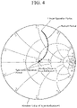
- FIG. 4 is a Smith chart illustrating input reflection of the peak amplifier 19 during the period from the linear operation to the saturation operation of the Doherty amplifier 10 illustrated in FIG. 1 .
- FIG. 4 illustrates input reflection of the peak amplifier 19 when the peak amplifier 19 is viewed from the input side of the coefficient adjustment line 16.
- the impedance at the center of the Smith chart illustrated in FIG. 4 is the input impedance Z pin0 at the saturation operation period of the peak amplifier 19.
- the impedance at the center of the Smith chart illustrated in FIG. 4 is normalized by the input impedance Z pin0 at the saturation operation period of the peak amplifier 19, and thus expressed as 1.0.
- the absolute value of the input reflection of the peak amplifier 19 is 0 as illustrated in FIG. 4 .
- the absolute value of the input reflection of the peak amplifier 19 is not 0 but nearly 1 as illustrated in FIG. 4 .
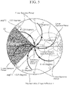
- FIG. 5 is a Smith chart illustrating input reflection of the peak amplifier 19 during the period from the linear operation to the saturation operation of the Doherty amplifier 10 illustrated in FIG. 1 .
- FIG. 5 illustrates input reflection of the peak amplifier 19 when the electrical length of the coefficient adjustment line 16 is 0 degrees, 30 degrees, 60 degrees, 90 degrees, 120 degrees, and 150 degrees.
- the input reflection of the peak amplifier 19 when the electrical length of the coefficient adjustment line 16 is 0 degrees is the same as the input reflection of the peak amplifier 19 illustrated in FIG. 4 .
- Each of the characteristic impedance of the coefficient adjustment line 16 and the characteristic impedance of the phase adjustment line 17 is the same as the input impedance Z pin0 at the saturation operation period of the peak amplifier 19 even if the electrical length of the coefficient adjustment line 16 varies. Therefore, when the electrical length of the coefficient adjustment line 16 varies, the phase of the input reflection at the linear operation period of the peak amplifier 19 changes.
- the input reflection of the peak amplifier 19 when the peak amplifier 19 is viewed from the input side of the coefficient adjustment line 16 rotates on the Smith chart depending on the electrical length of the coefficient adjustment line 16 as illustrated in FIG. 5 .
- phase of the input reflection of the peak amplifier 19 changes depending on the type of the transistor 19a included in the peak amplifier 19 or the type of each of the input matching circuit 19b and the output matching circuit 19c.
- the ideal operation means an operation satisfying the following two conditions.
- the peak amplifier 19 After the carrier amplifier 18 starts the signal amplification operation before the peak amplifier 19, the peak amplifier 19 rapidly starts the signal amplification operation from the backoff period between the linear operation and the saturation operation.
- the saturation operation period of the carrier amplifier 18 and the saturation operation period of the peak amplifier 19 occur simultaneously.
- a range 30 of the input reflection phase illustrated in FIG. 5 indicates a range of the input reflection phase necessary for achieving the ideal operation of the Doherty amplifier 10 illustrated in FIG. 1 when the peak amplifier 19 is viewed from the output terminal 11b of the Wilkinson divider 11.
- the range 30 is known when the Doherty amplifier 10 illustrated in FIG. 1 is designed.
- the range 30 of the input reflection phase when the peak amplifier 19 is viewed from the output terminal 11b illustrated in FIG. 1 is from 135 degrees to 220 degrees.
- the phase of the input reflection of the peak amplifier 19 is 120 degrees, the phase of the input reflection of the peak amplifier 19 is included in the range 30 of the input reflection phase of the Doherty amplifier 10.
- the electrical length of the coefficient adjustment line 16 is set so that the phase of the input reflection of the peak amplifier 19 is included in the range 30 of the input reflection phase upon designing the Doherty amplifier 10.
- the resistance value Riso of the resistor 14 is a value obtained by multiplying, by the proportionality coefficient w which is equal to or greater than 0 but less than 1, the sum of the input impedance Z cin0 at the saturation operation period of the carrier amplifier 18 and the input impedance Z pin0 at the saturation operation period of the peak amplifier 19.
- the Wilkinson divider 11 divides power Pi of the input signal into two.
- the Wilkinson divider 11 outputs the first signal as one of the divided signals from the output terminal 11a to the carrier amplifier 18 via the phase adjustment line 15.
- the Wilkinson divider 11 outputs the second signal as the other of the divided signals from the output terminal 11b to the peak amplifier 19 via the coefficient adjustment line 16 and the phase adjustment line 17.
- the carrier amplifier 18 amplifies the first signal output from the output terminal 1 1a of the Wilkinson divider 11 and then passing through the phase adjustment line 15.
- the carrier amplifier 18 outputs the amplified first signal to the output combining point 21 via the quarter wavelength line 20.
- the peak amplifier 19 amplifies the second signal output from the output terminal 11b of the Wilkinson divider 11 and then passing through each of the coefficient adjustment line 16 and the phase adjustment line 17.
- the peak amplifier 19 amplifies the second signal and outputs the amplified second signal to the output combining point 21.
- the amplified first signal output from the carrier amplifier 18 and then passing through the quarter wavelength line 20 and the amplified second signal output from the peak amplifier 19 are combined in phase at the output combining point 21.
- the combined signal (hereinafter, referred to as a "composite signal”) at the output combining point 21 is output to the load 2 via the output matching circuit 22.
- FIG. 6 is a configuration diagram illustrating the detail of the Wilkinson divider 11.
- Ii is a current of the signal input from the input terminal 1
- Vi is a voltage of the signal input from the input terminal 1.
- Zin is an input impedance of the Doherty amplifier 10 illustrated in FIG. 1
- ⁇ in is a reflection coefficient of the input signal at the Doherty amplifier 10 when the inside of the Doherty amplifier 10 is viewed from the input terminal 1.
- I 2 (- ⁇ /4) is a current of the signal input to the first transmission line 12
- V 2 (- ⁇ /4) is a voltage of the signal input to the first transmission line 12.
- I 2 (0) is a current of the signal output from the first transmission line 12
- V 2 (0) is a voltage of the signal output from the first transmission line 12.
- I 3 (- ⁇ /4) is a current of the signal input to the second transmission line 13
- V 3 (- ⁇ /4) is a voltage of the signal input to the second transmission line 13.
- I 3 (0) is a current of the signal output from the second transmission line 13
- V 3 (0) is a voltage of the signal output from the second transmission line 13.
- Iiso is a current flowing through the resistor 14
- I 2 (0)-I iso is a current of a signal output from the output terminal 11a to the phase adjustment line
- I 3 (0)+I iso is a current of a signal output from the output terminal 11b to the coefficient adjustment line 16.
- Zcin is an impedance when the carrier amplifier 18 is viewed from the output terminal 11a
- ⁇ cin is a reflection coefficient of the first signal in the carrier amplifier 18 when the carrier amplifier 18 is viewed from the output terminal 11a.
- Z pin is an impedance when the peak amplifier 19 is viewed from the output terminal 11b
- ⁇ pin is a reflection coefficient of the second signal at the peak amplifier 19 when the peak amplifier 19 is viewed from the output terminal 11b.
- Equation (1) The relationship among the impedance Zcin when the carrier amplifier 18 is viewed from the output terminal 11a, the input impedance Z cin0 at the saturation operation period of the carrier amplifier 18, and the reflection coefficient ⁇ cin of the first signal is expressed by Equation (1) below.
- Z cin Z cin 0 1 + ⁇ cin 1 ⁇ ⁇ cin
- Equation (2) The relationship among the impedance Z pin when the peak amplifier 19 is viewed from the output terminal 11b, the input impedance Z pin0 at the saturation operation period of the peak amplifier 19, and the reflection coefficient ⁇ pin of the second signal is expressed by Equation (2) below.
- Z pin Z pin 0 1 + ⁇ pin 1 ⁇ ⁇ pin
- the reflection coefficient ⁇ pin of the second signal at the peak amplifier 19 changes depending on the electrical length of the coefficient adjustment line 16 as illustrated in FIG. 5 .
- the power division ratio P 2 /P 3 of the signal in the Wilkinson divider 11 matches a desired power division ratio 1/K 2 .
- the power division ratio P 2 /P 3 is a power division ratio P 2 /P 3 with respect to the power P 2 of the first signal output from the output terminal 1 1a toward the carrier amplifier 18 and the power P 3 of the second signal output from the output terminal 11b toward the peak amplifier 19.
- the input impedance Zin of the Doherty amplifier 10 and the input impedance Z cin0 at the saturation operation period of the carrier amplifier 18 are known.
- the characteristic impedance Z 2 of the first transmission line 12 can be obtained by substituting the input impedance Zin and the input impedance Z cin0 into Equation (4) below.
- Z 2 Z in Z cin 0 1 + K 2
- the characteristic impedance Z 3 of the second transmission line 13 can be obtained by substituting the characteristic impedance Z 2 of the first transmission line 12 into Equation (5) below.
- Z 3 Z 2 K 2
- the power division ratio P 2 /P 3 during a period from the linear operation to the saturation operation of the Doherty amplifier 10 varies depending on the proportionality coefficient w as indicated by Equation (8).
- Fig. 7 is an explanatory diagram illustrating normalized power division ratios of a case where the proportionality coefficient w is changed from 0.2 to 1.8 in 0.2 steps with the phase of the reflection coefficient ⁇ pin when the peak amplifier 19 is viewed from the output terminal 11b of the Wilkinson divider 11 being 180 degrees.
- the horizontal axis represents an absolute value of the input reflection of the peak amplifier 19, and the peak amplifier 19 is saturated when the absolute value of the input reflection is 0. At the linear operation period of the peak amplifier 19, the absolute value of the input reflection is nearly 1.
- the vertical axis represents a normalized power division ratio in a range from the linear operation to the saturation operation of the Doherty amplifier 10.
- the normalized power division ratio is obtained by normalizing the power division ratio P 2 /P 3 by 1/K 2 . Therefore, when the normalized power division ratio is 1, the power division ratio P 2 /P 3 is 1/K 2 .
- the normalized power division ratio is 1, and the power division ratio P 2 /P 3 is 1/K 2 , despite the change of the proportionality coefficient w within the range from 0.2 to 1.8.
- the normalized power division ratio changes depending on the proportionality coefficient w as illustrated in FIG. 7 .
- the proportionality coefficient w is equal to or larger than 1
- the normalized power division ratio is always equal to or larger than 1, regardless of the absolute value of the input reflection of the peak amplifier 19, as illustrated in FIG. 7 .
- power to be distributed to the carrier amplifier 18 is more than power to be distributed to the peak amplifier 19 during the period from the linear operation to the saturation operation of the Doherty amplifier 10.
- the proportionality coefficient w is equal to or larger than 1, it is difficult to rapidly start the operation of the peak amplifier 19 at the backoff period. For this reason, the carrier amplifier 18 may reach saturation before the peak amplifier 19 reaches saturation, and thus, it is difficult to achieve an ideal operation of simultaneously saturating the carrier amplifier 18 and the peak amplifier 19.
- the normalized power division ratio is smaller than 1 within a range in which the absolute value of the input reflection of the peak amplifier 19 is larger than 0 and smaller than about 0.72, as illustrated in FIG. 7 .
- power to be distributed to the carrier amplifier 18 is more than power to be distributed to the peak amplifier 19 when the absolute value of the input reflection of the peak amplifier 19 is within a range of less than 1 and equal to or greater than about 0.72. That is, power to be distributed to the carrier amplifier 18 is more than power to be distributed to the peak amplifier 19 during the period from the linear operation to the backoff of the Doherty amplifier 10.
- power to be distributed to the peak amplifier 19 is more than power to be distributed to the carrier amplifier 18 when the absolute value of the input reflection of the peak amplifier 19 is within a range smaller than about 0.72 and larger than 0. That is, power to be distributed to the peak amplifier 19 is more than power to be distributed to the carrier amplifier 18 during the period from the backoff to the saturation operation of the Doherty amplifier 10.
- the carrier amplifier 18 it is possible to allow the carrier amplifier 18 to start the signal amplification operation before the peak amplifier 19, and then allow the peak amplifier 19 to rapidly start the signal amplification operation.
- the power division ratio P 2 /P 3 is the desired power division ratio 1/K 2 . That is, when the absolute value of the input reflection of the peak amplifier 19 is 0, both the carrier amplifier 18 and the peak amplifier 19 are saturated.
- FIG. 8 is an explanatory diagram illustrating a normalized power division ratio when the phase of the reflection coefficient T pin of the second signal is changed from 0 degrees to 180 degrees in steps of 22.5 degrees, in a case where the proportionality coefficient w is 0.4.
- the horizontal axis represents an absolute value of the input reflection of the peak amplifier 19, and the vertical axis represents a normalized power division ratio during the period from the linear operation to the saturation operation of the Doherty amplifier 10.
- the normalized power division ratio is obtained by normalizing the power division ratio P 2 /P 3 by 1/K 2 .
- Equation (8) indicating the power division ratio P 2 /P 3 during the period from the linear operation to the backoff represents an even function with respect to the phase of the reflection coefficient ⁇ pin of the second signal
- Equation (8) indicating the power division ratio P 2 /P 3 during the period from the linear operation to the backoff represents an even function with respect to the phase of the reflection coefficient ⁇ pin of the second signal
- phase of the reflection coefficient ⁇ pin of the second signal is within a range from 270 degrees to 360 degrees, there is no absolute value of the input reflection of the peak amplifier 19 at which the normalized power division ratio is smaller than 1.
- FIG. 9 is an explanatory diagram illustrating a gain with respect to the output power of the Doherty amplifier 10 that satisfies the phase condition of the reflection coefficient ⁇ pin by which the ideal operation can be achieved and that has the proportionality coefficient w smaller than 1 and equal to or greater than 0.
- the peak amplifier cannot rapidly start the signal amplification operation at the backoff, so that the gain rapidly decreases during the period from the backoff to the saturation operation.
- gain characteristics are nonlinear.
- the peak amplifier 19 can rapidly start signal amplification operation at the backoff, so that flatness of gain can be maintained during the period from the backoff to the saturation operation.
- the carrier amplifier 18 and the peak amplifier 19 can be saturated at the same time, and thus, the saturation output power increases as compared with the Doherty amplifier described in Patent Literature 1.
- the Doherty amplifier described in Patent Literature 1 includes a delay circuit in order to address a problem that the gain of the combined signal is reduced because the two divided signals are output from the isolation resistance variable divider before the control circuit completes varying the division ratio.
- the Doherty amplifier 10 illustrated in FIG. 1 prevents a decrease in gain of a combined signal without a control circuit as described in Patent Literature 1, so that the Doherty amplifier 10 illustrated in FIG. 1 does not need to have a delay circuit as described in Patent Literature 1. Therefore, this Doherty amplifier 10 illustrated in FIG. 1 does not have a problem that the Doherty amplifier cannot output an amplified signal until the delay time of the delay circuit elapses after the input signal is input to the delay circuit.
- the Doherty amplifier 10 illustrated in FIG. 1 does not include a detection circuit, a control circuit, and a delay circuit as described in Patent Literature 1, it is possible to achieve miniaturization and simplification and to reduce power consumption as compared with the Doherty amplifier described in Patent Literature 1.
- the Doherty amplifier 10 is configured in such a manner that: the ratio Z 3 /Z 2 of the characteristic impedance Z 3 of the second transmission line 13 to the characteristic impedance Z 2 of the first transmission line 12 is the power division ratio P 2 /P 3 of a signal to be amplified between the carrier amplifier 18 and the peak amplifier 19 when both of the carrier amplifier 18 and the peak amplifier 19 are saturated; and the resistance value Riso of the resistor 14 is a value obtained by multiplying, by the proportionality coefficient w which is equal to or greater than 0 but less than 1, the sum of the input impedance Z cin0 of the carrier amplifier 18 when the carrier amplifier 18 reaches saturation and the input impedance Z pin0 of the peak amplifier 19 when the peak amplifier 19 reaches saturation.
- the Doherty amplifier 10 can prevent a decrease in gain of the combined signal of the signal output from the carrier amplifier 18 and the signal output from the peak amplifier 19 during the period from the backoff to the saturation operation without having a delay circuit that delays the signal to be amplified.
- a second embodiment will describe a Doherty amplifier 10 in which a Wilkinson divider 11 includes capacitors 41 and 42 connected in series with a resistor 40.
- FIG. 10 is a configuration diagram illustrating the Wilkinson divider 11 of the Doherty amplifier 10 according to the second embodiment.
- elements that are the same as or correspond to the elements in FIG. 1 are identified by the same reference numerals, and thus, the description thereof will be omitted.
- the resistor 40 has a parasitic inductance 40b in addition to a resistor 40a having a resistance value of Riso.
- a first end of the capacitor 41 is connected to each of the second end of the first transmission line 12 and the output terminal 11a, and a second end of the capacitor 41 is connected to a first end of the resistor 40.
- a first end of the capacitor 42 is connected to the second end of the second transmission line 13 and the output terminal 11b, and a second end of the capacitor 42 is connected to a second end of the resistor 40.
- Each of the capacitor 41 and the capacitor 42 is provided to compensate for phase rotation of the first signal and the second signal which is caused by the resistor 40 having the parasitic inductance 40b.
- the Wilkinson divider 11 includes the capacitors 41 and 42 connected in series with the resistor 40, a decrease in gain of the combined signal can be prevented, as in the Doherty amplifier 10 illustrated in FIG. 1 , despite the resistor 40 having the parasitic inductance 40b.
- a communication device including the Doherty amplifier illustrated in FIG. 1 may be configured as an amplifier that amplifies the communication signal.
- FIG. 11 is a configuration diagram illustrating a communication device including the Doherty amplifier 10 illustrated in FIG. 1 .
- the Doherty amplifier illustrated in FIG. 1 does not include a delay circuit as described in Patent Literature 1. Therefore, the communication device illustrated in FIG. 11 can amplify the communication signal without a delay of the communication signal corresponding to the delay time of the delay circuit.
- the communication device illustrated in FIG. 11 includes the Doherty amplifier 10 illustrated in FIG. 1 , but may include the Doherty amplifier 10 including the Wilkinson divider 11 illustrated in FIG. 10 .
- the present disclosure is suitable for a Doherty amplifier and a communication device.
Landscapes
- Engineering & Computer Science (AREA)
- Power Engineering (AREA)
- Amplifiers (AREA)
- Microwave Amplifiers (AREA)
Abstract
Description
- The present disclosure relates to a Doherty amplifier and a communication device.
-
Patent Literature 1 below discloses a Doherty amplifier including an isolation resistance variable divider that divides an input signal into two and outputs the two divided signals, a carrier amplifier circuit that amplifies one of the two signals output from the isolation resistance variable divider, and a peak amplifier circuit that amplifies the other of the two signals. The Doherty amplifier also includes a detection circuit that converts power of an input signal into a voltage and outputs the voltage as an input power level, and a control circuit that varies a division ratio of an input signal in the isolation resistance variable divider by controlling a resistance value of a variable resistor included in the isolation resistance variable divider according to the input power level output from the detection circuit. Since the Doherty amplifier includes the detection circuit and the control circuit, the Doherty amplifier can prevent a decrease in gain of the amplified signal due to a division loss in the isolation resistance variable divider. That is, the Doherty amplifier can prevent a decrease in gain of a combined signal of the signal output from the carrier amplifier circuit and the signal output from the peak amplifier circuit during a period from a backoff to a saturation operation. - In addition, the Doherty amplifier includes a delay circuit that delays the input signal by a time required from when the input signal is input to the detection circuit to when the control circuit finishes varying the division ratio.
- Patent Literature 1:
JP 2008-125044 A - The Doherty amplifier disclosed in
Patent Literature 1 includes a delay circuit that delays an input signal. Therefore, this Doherty amplifier has a problem that the Doherty amplifier cannot output the amplified signal until the delay time of the delay circuit elapses after the input signal is input to the delay circuit. - The present disclosure has been accomplished to solve the above problems, and an object of the present disclosure is to obtain a Doherty amplifier capable of preventing a decrease in gain of a combined signal of a signal output from a carrier amplifier and a signal output from a peak amplifier during a period from a backoff to a saturation operation without having a delay circuit that delays a signal to be amplified.
- The Doherty amplifier according to the present disclosure includes: a first transmission line having a first end connected to an input terminal to which a signal to be amplified is input; a second transmission line having a first end connected to the input terminal; a resistor connected between a second end of the first transmission line and a second end of the second transmission line; a carrier amplifier to amplify a signal output from the second end of the first transmission line and output the amplified signal to an output combining point; and a peak amplifier to amplify a signal output from the second end of the second transmission line and output the amplified signal to the output combining point, wherein a ratio of a characteristic impedance of the second transmission line to a characteristic impedance of the first transmission line is a power division ratio of the signal to be amplified between the carrier amplifier and the peak amplifier when both of the carrier amplifier and the peak amplifier are saturated, and a resistance value of the resistor is a value obtained by multiplying, by a proportionality coefficient that is equal to or greater than 0 but less than 1, a sum of the input impedance of the carrier amplifier when the carrier amplifier reaches saturation and the input impedance of the peak amplifier when the peak amplifier reaches saturation.
- According to the present disclosure, the Doherty amplifier is configured in such a manner that: the ratio of the characteristic impedance of the second transmission line to the characteristic impedance of the first transmission line is a power division ratio of the signal to be amplified between the carrier amplifier and the peak amplifier when both of the carrier amplifier and the peak amplifier are saturated; and a resistance value of the resistor is a value obtained by multiplying, by a proportionality coefficient that is equal to or greater than 0 but less than 1, a sum of the input impedance of the carrier amplifier when the carrier amplifier reaches saturation and the input impedance of the peak amplifier when the peak amplifier reaches saturation. Therefore, the Doherty amplifier according to the present disclosure can prevent a decrease in gain of a combined signal of a signal output from the carrier amplifier and a signal output from the peak amplifier during a period from a backoff to a saturation operation without having a delay circuit that delays the signal to be amplified.
-
-
FIG. 1 is a configuration diagram illustrating a Dohertyamplifier 10 according to a first embodiment. -
FIG. 2 is a configuration diagram illustrating the inside of acarrier amplifier 18. -
FIG. 3 is a configuration diagram illustrating the inside of apeak amplifier 19. -
FIG. 4 is a Smith chart illustrating input reflection of thepeak amplifier 19 during a period from a linear operation to a saturation operation of the Doherty amplifier illustrated inFIG. 1 . -
FIG. 5 is a Smith chart illustrating input reflection of thepeak amplifier 19 during a period from a linear operation to a saturation operation of the Doherty amplifier illustrated inFIG. 1 . -
FIG. 6 is a configuration diagram illustrating details of a Wilkinsondivider 11. -
FIG. 7 is an explanatory diagram illustrating normalized power division ratios of a case where a proportionality coefficient w is changed from 0.2 to 1.8 in 0.2 steps with the phase of a reflection coefficient Γpin when thepeak amplifier 19 is viewed from anoutput terminal 11b of the Wilkinsondivider 11 being 180 degrees. -
FIG. 8 is an explanatory diagram illustrating a normalized power division ratio when the phase of the reflection coefficient Γpin of a second signal is changed from 0 degrees to 180 degrees in steps of 22.5 degrees, in a case where the proportionality coefficient w is 0.4. -
FIG. 9 is an explanatory diagram illustrating a gain with respect to output power of the Dohertyamplifier 10 that satisfies a phase condition of the reflection coefficient Γpin by which an ideal operation can be achieved and that has a proportionality coefficient w equal to or greater than 0 but less than 1. -
FIG. 10 is a configuration diagram illustrating a Wilkinsondivider 11 of a Dohertyamplifier 10 according to a second embodiment. -
FIG. 11 is a configuration diagram illustrating a communication device including the Dohertyamplifier 10 illustrated inFIG. 1 . - In order to describe the present disclosure in more detail, a mode for carrying out the present disclosure will now be described with reference to the accompanying drawings.
-
FIG. 1 is a configuration diagram illustrating a Dohertyamplifier 10 according to a first embodiment. - In
FIG. 1 , aninput terminal 1 is a terminal for receiving a signal to be amplified from the outside of the Dohertyamplifier 10. - A
load 2 is an external load of the Dohertyamplifier 10. A first end of theload 2 is connected to a second end of an output matchingcircuit 22 to be described later of the Dohertyamplifier 10, and a second end of theload 2 is grounded. - The Doherty
amplifier 10 amplifies the signal input from theinput terminal 1 and outputs the amplified signal to theload 2. The power of the signal input from theinput terminal 1 is Pi. - A Wilkinson
divider 11 includes afirst transmission line 12, asecond transmission line 13, and aresistor 14. - The Wilkinson
divider 11 divides the power Pi of the signal input from theinput terminal 1 into two. The Wilkinson divider 11 outputs a first signal from anoutput terminal 11a to aphase adjustment line 15 to be described later as one of the divided signals and outputs a second signal from anoutput terminal 11b to acoefficient adjustment line 16 to be described later as the other signal of the divided signals. - A first end of the
first transmission line 12 is connected to theinput terminal 1, and a second end of thefirst transmission line 12 is connected to each of a first end of theresistor 14 and theoutput terminal 11a. - The
first transmission line 12 has an electrical length of one-quarter wavelength (hereinafter referred to as "λ/4") at the frequency of the signal input from theinput terminal 1. The electrical length of λ/4 is an electrical length of 90 degrees. The characteristic impedance of thefirst transmission line 12 is Z2. - A first end of the
second transmission line 13 is connected to theinput terminal 1, and a second end of thesecond transmission line 13 is connected to each of a second end of theresistor 14 and theoutput terminal 11b. - The
second transmission line 13 has an electrical length of λ/4 at the frequency of the signal input from theinput terminal 1. The characteristic impedance of thesecond transmission line 13 is Z3. - A ratio Z3/Z2 of the characteristic impedance Z3 of the
second transmission line 13 to the characteristic impedance Z2 of thefirst transmission line 12 is a power division ratio P2/P3 of a signal to be amplified between thecarrier amplifier 18 and thepeak amplifier 19 when both of thecarrier amplifier 18 and thepeak amplifier 19 are saturated. P2 is power of a signal output from theoutput terminal 11a when thecarrier amplifier 18 is saturated. P3 is power of a signal output from theoutput terminal 11b when thepeak amplifier 19 is saturated. - The
resistor 14 is connected between the second end of thefirst transmission line 12 and the second end of thesecond transmission line 13. - The resistance value Riso of the
resistor 14 is a value obtained by multiplying, by a proportionality coefficient w which is equal to or greater than 0 but less than 1, the sum of an input impedance Zcino of thecarrier amplifier 18 when thecarrier amplifier 18 reaches saturation and an input impedance Zpin0 of thepeak amplifier 19 when thepeak amplifier 19 reaches saturation. - Hereinafter, the input impedance Zcino of the carrier amplifier 18 when the
carrier amplifier 18 reaches saturation may be referred to as an input impedance at a saturation operation period of thecarrier amplifier 18. In addition, the input impedance Zpin0 of thepeak amplifier 19 when thepeak amplifier 19 reaches saturation may be referred to as an input impedance at a saturation operation period of thepeak amplifier 19. - The saturation operation period of the
carrier amplifier 18 means a period at which the amplification operation of the carrier amplifier 18 on the first signal reaches saturation, and the saturation operation period of thepeak amplifier 19 means a period at which the amplification operation of thepeak amplifier 19 on the second signal reaches saturation. - A first end of the
phase adjustment line 15 is connected to the second end of thefirst transmission line 12 and the first end of theresistor 14 via theoutput terminal 11a, and a second end of thephase adjustment line 15 is connected to an input side of thecarrier amplifier 18. Thephase adjustment line 15 has the same electrical length as the electrical length of thecoefficient adjustment line 16. Here, the concept of "the same electrical length" is not limited to a case where the electrical lengths are exactly the same, but includes a case where the electrical lengths are different from each other as long as there is no practical problem. - The characteristic impedance of the
phase adjustment line 15 is the same as the input impedance Zcin0 of thecarrier amplifier 18. The concept of "the same electrical length" here is not limited to a case where the characteristic impedance of thephase adjustment line 15 and the input impedance Zcin0 of thecarrier amplifier 18 are exactly the same, but includes a case where they are different from each other as long as there is no practical problem. - A first end of the
coefficient adjustment line 16 is connected to each of the second end of thesecond transmission line 13 and the second end of theresistor 14 via theoutput terminal 11b, and a second end of thecoefficient adjustment line 16 is connected to a first end of aphase adjustment line 17 to be described later. Thecoefficient adjustment line 16 is a line for adjusting a reflection coefficient Γpin of the second signal at thepeak amplifier 19, which is obtained when thepeak amplifier 19 is viewed from the second end of thesecond transmission line 13. - The first end of the
phase adjustment line 17 is connected to the second end of thecoefficient adjustment line 16, and a second end of thephase adjustment line 17 is connected to an input side of thepeak amplifier 19. Thephase adjustment line 17 has an electrical length of λ/4 at the frequency of the signal input from theinput terminal 1. - Each of the characteristic impedance of the
coefficient adjustment line 16 and the characteristic impedance of thephase adjustment line 17 is the same as the input impedance Zpin0 at the saturation operation period of thepeak amplifier 19. The concept of "the same" here is not limited to a case where the impedances are exactly the same, but includes a case where the impedances are different from each other as long as there is no practical problem. - Since the
phase adjustment line 17 is inserted between thecoefficient adjustment line 16 and thepeak amplifier 19, a phase difference between a path from thecarrier amplifier 18 to anoutput combining point 21 to be described later and a path from thepeak amplifier 19 to theoutput combining point 21 is compensated for. - The input side of the
carrier amplifier 18 is connected to the second end of thephase adjustment line 15, and an output side of thecarrier amplifier 18 is connected to a first end of aquarter wavelength line 20 described later. Thecarrier amplifier 18 amplifies the first signal that is output from the second end of thefirst transmission line 12 and then passes through thephase adjustment line 15, and outputs the amplified first signal to theoutput combining point 21 via thequarter wavelength line 20. - Since the
carrier amplifier 18 is biased to class AB, the input impedance Zcin0 of thecarrier amplifier 18 does not change during the period from a linear operation to the saturation operation. The linear operation period means a period at which thecarrier amplifier 18 starts an amplification operation on the first signal, and at the linear operation period, thepeak amplifier 19 has not started an amplification operation on the second signal. - In the
Doherty amplifier 10 illustrated inFIG. 1 , the saturation operation period of thecarrier amplifier 18 and the period the saturation operation of thepeak amplifier 19 occur simultaneously. The concept of "simultaneously" here is not limited to a case where the periods of the saturation operation are exactly the same, but includes a case where the periods of the saturation operation are different from each other as long as there is no practical problem. - There is a backoff period between the linear operation and the saturation operation, and the backoff means a period during which the amplification operation of the
peak amplifier 19 for the second signal is rapidly started. -
FIG. 2 is a configuration diagram illustrating the inside of thecarrier amplifier 18. - As illustrated in
FIG. 2 , thecarrier amplifier 18 includes, in addition to atransistor 18a that amplifies the first signal, aninput matching circuit 18b connected to an input side of thetransistor 18a and anoutput matching circuit 18c connected to an output side of thetransistor 18a. - In addition, as illustrated in
FIG. 2 , thecarrier amplifier 18 includes astabilization circuit 18d that blocks passage of frequency components other than a desired frequency component included in the first signal and allows passage of the desired frequency component. - The
stabilization circuit 18d is connected between thephase adjustment line 15 and theinput matching circuit 18b, and is implemented by, for example, a low-pass filter, a band-pass filter, or a high-pass filter. - In
FIG. 2 , thestabilization circuit 18d is connected between thephase adjustment line 15 and theinput matching circuit 18b. However, this is merely an example, and thestabilization circuit 18d may be connected between theinput matching circuit 18b and thetransistor 18a, between thetransistor 18a and theoutput matching circuit 18c, or between theoutput matching circuit 18c and thequarter wavelength line 20. - The input side of the
peak amplifier 19 is connected to the second end of thephase adjustment line 17, and the output side of thepeak amplifier 19 is connected to theoutput combining point 21. Thepeak amplifier 19 amplifies the second signal that is output from the second end of thesecond transmission line 13 and then passes through thecoefficient adjustment line 16 and thephase adjustment line 17, and outputs the amplified second signal to theoutput combining point 21. - Since the
peak amplifier 19 is biased to class C, the input impedance Zpin0 of thepeak amplifier 19 greatly changes during the period from the linear operation to the saturation operation. -
FIG. 3 is a configuration diagram illustrating the inside of thepeak amplifier 19. - As illustrated in
FIG. 3 , thepeak amplifier 19 includes, in addition to atransistor 19a that amplifies the second signal, aninput matching circuit 19b connected to an input side of thetransistor 19a, and anoutput matching circuit 19c connected to an output side of thetransistor 19a. - Furthermore, as illustrated in
FIG. 3 , thepeak amplifier 19 includes astabilization circuit 19d that blocks passage of frequency components other than a desired frequency component included in the second signal and allows passage of the desired frequency component. - The
stabilization circuit 19d is connected between thephase adjustment line 17 and theinput matching circuit 19b, and is implemented by, for example, a low-pass filter, a band-pass filter, or a high-pass filter. - In
FIG. 2 , thestabilization circuit 19d is connected between thephase adjustment line 17 and theinput matching circuit 19b. However, this is merely an example, and thestabilization circuit 19d may be connected between theinput matching circuit 19b and thetransistor 19a, between thetransistor 19a and theoutput matching circuit 19c, or between theoutput matching circuit 19c and theoutput combining point 21. - The first end of the
quarter wavelength line 20 is connected to the output side of thecarrier amplifier 18, and a second end of thequarter wavelength line 20 is connected to theoutput combining point 21. Thequarter wavelength line 20 has an electrical length of λ/4 at the frequency of the signal input from theinput terminal 1. Thequarter wavelength line 20 is connected between thecarrier amplifier 18 and theoutput combining point 21 in order to modulate the impedance at the backoff period. - The output side of the
peak amplifier 19 and the second end of thequarter wavelength line 20 are connected to theoutput combining point 21. The amplified first signal output from thecarrier amplifier 18 and then passing through thequarter wavelength line 20 and the amplified second signal output from thepeak amplifier 19 are combined in phase at theoutput combining point 21. - A first end of the
output matching circuit 22 is connected to theoutput combining point 21, and the second end of theoutput matching circuit 22 is connected to theload 2. Theoutput matching circuit 22 is provided to match the impedance on the output side of theDoherty amplifier 10 with the impedance of theload 2. - Since the
carrier amplifier 18 is biased to class AB, the input impedance Zcin0 of thecarrier amplifier 18 does not change during the period from the linear operation to the saturation operation. The characteristic impedance of thephase adjustment line 15 is the same as the input impedance Zcin0 of thecarrier amplifier 18 during the period from the linear operation to the saturation operation of thecarrier amplifier 18. - Therefore, the absolute value of the input reflection when the
carrier amplifier 18 is viewed from theoutput terminal 1 1a of theWilkinson divider 11 is 0 during the period from the linear operation to the saturation operation of thecarrier amplifier 18. - Each of the characteristic impedance of the
coefficient adjustment line 16 and the characteristic impedance of thephase adjustment line 17 is the same as the input impedance Zpin0 at the saturation operation period of thepeak amplifier 19. - Unlike the
carrier amplifier 18, thepeak amplifier 19 is biased to class C, so that the input impedance Zpin0 of thepeak amplifier 19 greatly changes during the period from the linear operation to the saturation operation. - Therefore, the characteristic impedance of the
coefficient adjustment line 16 and the characteristic impedance of thephase adjustment line 17 are different from the input impedance Zpin0 of thepeak amplifier 19 at a period other than the saturation operation period of thepeak amplifier 19. -
FIG. 4 is a Smith chart illustrating input reflection of thepeak amplifier 19 during the period from the linear operation to the saturation operation of theDoherty amplifier 10 illustrated inFIG. 1 .FIG. 4 illustrates input reflection of thepeak amplifier 19 when thepeak amplifier 19 is viewed from the input side of thecoefficient adjustment line 16. - The impedance at the center of the Smith chart illustrated in
FIG. 4 is the input impedance Zpin0 at the saturation operation period of thepeak amplifier 19. The impedance at the center of the Smith chart illustrated inFIG. 4 is normalized by the input impedance Zpin0 at the saturation operation period of thepeak amplifier 19, and thus expressed as 1.0. - At the saturation operation period of the
peak amplifier 19, the absolute value of the input reflection of thepeak amplifier 19 is 0 as illustrated inFIG. 4 . - At the linear operation period of the
peak amplifier 19, the absolute value of the input reflection of thepeak amplifier 19 is not 0 but nearly 1 as illustrated inFIG. 4 . -
FIG. 5 is a Smith chart illustrating input reflection of thepeak amplifier 19 during the period from the linear operation to the saturation operation of theDoherty amplifier 10 illustrated inFIG. 1 . -
FIG. 5 illustrates input reflection of thepeak amplifier 19 when the electrical length of thecoefficient adjustment line 16 is 0 degrees, 30 degrees, 60 degrees, 90 degrees, 120 degrees, and 150 degrees. The input reflection of thepeak amplifier 19 when the electrical length of thecoefficient adjustment line 16 is 0 degrees is the same as the input reflection of thepeak amplifier 19 illustrated inFIG. 4 . - Each of the characteristic impedance of the
coefficient adjustment line 16 and the characteristic impedance of thephase adjustment line 17 is the same as the input impedance Zpin0 at the saturation operation period of thepeak amplifier 19 even if the electrical length of thecoefficient adjustment line 16 varies. Therefore, when the electrical length of thecoefficient adjustment line 16 varies, the phase of the input reflection at the linear operation period of thepeak amplifier 19 changes. - Therefore, the input reflection of the
peak amplifier 19 when thepeak amplifier 19 is viewed from the input side of thecoefficient adjustment line 16 rotates on the Smith chart depending on the electrical length of thecoefficient adjustment line 16 as illustrated inFIG. 5 . - Note that the phase of the input reflection of the
peak amplifier 19 changes depending on the type of thetransistor 19a included in thepeak amplifier 19 or the type of each of theinput matching circuit 19b and theoutput matching circuit 19c. - There is a range of the input reflection phase for achieving an ideal operation of the
Doherty amplifier 10 illustrated inFIG. 1 . - The ideal operation means an operation satisfying the following two conditions.
- After the
carrier amplifier 18 starts the signal amplification operation before thepeak amplifier 19, thepeak amplifier 19 rapidly starts the signal amplification operation from the backoff period between the linear operation and the saturation operation. - The saturation operation period of the
carrier amplifier 18 and the saturation operation period of thepeak amplifier 19 occur simultaneously. - A
range 30 of the input reflection phase illustrated inFIG. 5 indicates a range of the input reflection phase necessary for achieving the ideal operation of theDoherty amplifier 10 illustrated inFIG. 1 when thepeak amplifier 19 is viewed from theoutput terminal 11b of theWilkinson divider 11. Therange 30 is known when theDoherty amplifier 10 illustrated inFIG. 1 is designed. - In the example of
FIG. 5 , therange 30 of the input reflection phase when thepeak amplifier 19 is viewed from theoutput terminal 11b illustrated inFIG. 1 is from 135 degrees to 220 degrees. - In the example of
FIG. 5 , when the phase of the input reflection of thepeak amplifier 19 is 120 degrees, the phase of the input reflection of thepeak amplifier 19 is included in therange 30 of the input reflection phase of theDoherty amplifier 10. - In the
Doherty amplifier 10 illustrated inFIG. 1 , in order to satisfy the condition (1), the electrical length of thecoefficient adjustment line 16 is set so that the phase of the input reflection of thepeak amplifier 19 is included in therange 30 of the input reflection phase upon designing theDoherty amplifier 10. - In addition, in the
Doherty amplifier 10 illustrated inFIG. 1 , in order to satisfy both the condition (1) and the condition (2), the resistance value Riso of theresistor 14 is a value obtained by multiplying, by the proportionality coefficient w which is equal to or greater than 0 but less than 1, the sum of the input impedance Zcin0 at the saturation operation period of thecarrier amplifier 18 and the input impedance Zpin0 at the saturation operation period of thepeak amplifier 19. - Next, the operation of the
Doherty amplifier 10 illustrated inFIG. 1 will be described. - When a signal to be amplified is input from the
input terminal 1, theWilkinson divider 11 divides power Pi of the input signal into two. - The
Wilkinson divider 11 outputs the first signal as one of the divided signals from theoutput terminal 11a to thecarrier amplifier 18 via thephase adjustment line 15. - In addition, the
Wilkinson divider 11 outputs the second signal as the other of the divided signals from theoutput terminal 11b to thepeak amplifier 19 via thecoefficient adjustment line 16 and thephase adjustment line 17. - The details of the operation of the
Wilkinson divider 11 will be described later. - The
carrier amplifier 18 amplifies the first signal output from theoutput terminal 1 1a of theWilkinson divider 11 and then passing through thephase adjustment line 15. - The
carrier amplifier 18 outputs the amplified first signal to theoutput combining point 21 via thequarter wavelength line 20. - The
peak amplifier 19 amplifies the second signal output from theoutput terminal 11b of theWilkinson divider 11 and then passing through each of thecoefficient adjustment line 16 and thephase adjustment line 17. - The
peak amplifier 19 amplifies the second signal and outputs the amplified second signal to theoutput combining point 21. - The amplified first signal output from the
carrier amplifier 18 and then passing through thequarter wavelength line 20 and the amplified second signal output from thepeak amplifier 19 are combined in phase at theoutput combining point 21. - The combined signal (hereinafter, referred to as a "composite signal") at the
output combining point 21 is output to theload 2 via theoutput matching circuit 22. - Next, the operation of the
Wilkinson divider 11 will be described in detail. -
FIG. 6 is a configuration diagram illustrating the detail of theWilkinson divider 11. - In
FIG. 6 , Ii is a current of the signal input from theinput terminal 1, and Vi is a voltage of the signal input from theinput terminal 1. - Zin is an input impedance of the
Doherty amplifier 10 illustrated inFIG. 1 , and Γin is a reflection coefficient of the input signal at theDoherty amplifier 10 when the inside of theDoherty amplifier 10 is viewed from theinput terminal 1. - I2(-λ/4) is a current of the signal input to the
first transmission line 12, and V2(-λ/4) is a voltage of the signal input to thefirst transmission line 12. - I2(0) is a current of the signal output from the
first transmission line 12, and V2(0) is a voltage of the signal output from thefirst transmission line 12. - I3(-λ/4) is a current of the signal input to the
second transmission line 13, and V3(-λ/4) is a voltage of the signal input to thesecond transmission line 13. - I3(0) is a current of the signal output from the
second transmission line 13, and V3(0) is a voltage of the signal output from thesecond transmission line 13. - Iiso is a current flowing through the
resistor 14, I2(0)-Iiso is a current of a signal output from theoutput terminal 11a to thephase adjustment line 15, and I3(0)+Iiso is a current of a signal output from theoutput terminal 11b to thecoefficient adjustment line 16. - Zcin is an impedance when the
carrier amplifier 18 is viewed from theoutput terminal 11a, and Γcin is a reflection coefficient of the first signal in thecarrier amplifier 18 when thecarrier amplifier 18 is viewed from theoutput terminal 11a. - Zpin is an impedance when the
peak amplifier 19 is viewed from theoutput terminal 11b, and Γpin is a reflection coefficient of the second signal at thepeak amplifier 19 when thepeak amplifier 19 is viewed from theoutput terminal 11b. - The relationship among the impedance Zcin when the
carrier amplifier 18 is viewed from theoutput terminal 11a, the input impedance Zcin0 at the saturation operation period of thecarrier amplifier 18, and the reflection coefficient Γcin of the first signal is expressed by Equation (1) below.
- The relationship among the impedance Zpin when the
peak amplifier 19 is viewed from theoutput terminal 11b, the input impedance Zpin0 at the saturation operation period of thepeak amplifier 19, and the reflection coefficient Γpin of the second signal is expressed by Equation (2) below.
- Since the input impedance Zcin0 of the
carrier amplifier 18 does not change during the period from the linear operation to the saturation operation, the input reflection coefficient of thecarrier amplifier 18 is constantly Γcin = 0. - Since the input impedance Zpin0 of the
peak amplifier 19 changes during the period from the linear operation to the saturation operation, the reflection coefficient Γpin of the second signal at thepeak amplifier 19 changes depending on the electrical length of thecoefficient adjustment line 16 as illustrated inFIG. 5 . - Hereinafter, the operation of the
Wilkinson divider 11 when both thecarrier amplifier 18 and thepeak amplifier 19 are saturated and the operation of theWilkinson divider 11 during the period from the linear operation to the saturation operation will be described. - [Operation of
Wilkinson divider 11 when bothcarrier amplifier 18 andpeak amplifier 19 are saturated] - When both the
carrier amplifier 18 and thepeak amplifier 19 are saturated, the power division ratio P2/P3 of the signal in theWilkinson divider 11 matches a desiredpower division ratio 1/K2. The power division ratio P2/P3 is a power division ratio P2/P3 with respect to the power P2 of the first signal output from theoutput terminal 1 1a toward thecarrier amplifier 18 and the power P3 of the second signal output from theoutput terminal 11b toward thepeak amplifier 19. - When both the
carrier amplifier 18 and thepeak amplifier 19 are saturated, the relationship among the ratio Z3/Z2 of the characteristic impedance Z3 of thesecond transmission line 13 to the characteristic impedance Z2 of thefirst transmission line 12, the ratio Zpin0/Zcin0 of the input impedance Zpin0 of thepeak amplifier 19 to the input impedance Zcin0 of thecarrier amplifier 18, and the power division ratio P2/P3 is expressed by Equation (3) below.
- When the
Doherty amplifier 10 illustrated inFIG. 1 is designed, the input impedance Zin of theDoherty amplifier 10 and the input impedance Zcin0 at the saturation operation period of thecarrier amplifier 18 are known. - Therefore, the characteristic impedance Z2 of the
first transmission line 12 can be obtained by substituting the input impedance Zin and the input impedance Zcin0 into Equation (4) below.
- The characteristic impedance Z3 of the
second transmission line 13 can be obtained by substituting the characteristic impedance Z2 of thefirst transmission line 12 into Equation (5) below.
- When the resistance value Riso of the
resistor 14 matches the sum of the input impedance Zcin0 and the input impedance Zpin0 as indicated in Equation (6) below, no current flows through theresistor 14, and thus theoutput terminal 11a and theoutput terminal 11b are isolated.
- When the resistance value Riso of the
resistor 14 is a value obtained by multiplying the resistance value Riso indicated in Equation (6) by a proportionality coefficient w which is equal to or greater than 0 but less than 1 as indicated in Equation (7) below, a current flows through theresistor 14. The current flowing through theresistor 14 changes the power division ratio P2/P3 at a period other than the saturation operation period of theDoherty amplifier 10 illustrated inFIG. 1 . However, when both thecarrier amplifier 18 and thepeak amplifier 19 are saturated, the power division ratio P2/P3 does not change and matches the desiredpower division ratio 1/K2 even if the current flows through theresistor 14.
- [Operation of
Wilkinson divider 11 during a period from linear operation to saturation operation] - The power division ratio P2/P3 during a period from the linear operation to the saturation operation of the
Doherty amplifier 10 is expressed by Equation (8) below.

- The power division ratio P2/P3 during a period from the linear operation to the saturation operation of the
Doherty amplifier 10 varies depending on the proportionality coefficient w as indicated by Equation (8). -
Fig. 7 is an explanatory diagram illustrating normalized power division ratios of a case where the proportionality coefficient w is changed from 0.2 to 1.8 in 0.2 steps with the phase of the reflection coefficient Γpin when thepeak amplifier 19 is viewed from theoutput terminal 11b of theWilkinson divider 11 being 180 degrees. - In
FIG. 7 , the horizontal axis represents an absolute value of the input reflection of thepeak amplifier 19, and thepeak amplifier 19 is saturated when the absolute value of the input reflection is 0. At the linear operation period of thepeak amplifier 19, the absolute value of the input reflection is nearly 1. - The vertical axis represents a normalized power division ratio in a range from the linear operation to the saturation operation of the
Doherty amplifier 10. The normalized power division ratio is obtained by normalizing the power division ratio P2/P3 by 1/K2. Therefore, when the normalized power division ratio is 1, the power division ratio P2/P3 is 1/K2. - As illustrated in
FIG. 7 , when thepeak amplifier 19 is saturated, the normalized power division ratio is 1, and the power division ratio P2/P3 is 1/K2, despite the change of the proportionality coefficient w within the range from 0.2 to 1.8. - When the absolute value of the input reflection of the
peak amplifier 19 is larger than 0 and thepeak amplifier 19 is not at the saturation operation period, the normalized power division ratio changes depending on the proportionality coefficient w as illustrated inFIG. 7 . - In a case where the proportionality coefficient w is equal to or larger than 1, the normalized power division ratio is always equal to or larger than 1, regardless of the absolute value of the input reflection of the
peak amplifier 19, as illustrated inFIG. 7 . Thus, power to be distributed to thecarrier amplifier 18 is more than power to be distributed to thepeak amplifier 19 during the period from the linear operation to the saturation operation of theDoherty amplifier 10. - Therefore, when the proportionality coefficient w is equal to or larger than 1, it is difficult to rapidly start the operation of the
peak amplifier 19 at the backoff period. For this reason, thecarrier amplifier 18 may reach saturation before thepeak amplifier 19 reaches saturation, and thus, it is difficult to achieve an ideal operation of simultaneously saturating thecarrier amplifier 18 and thepeak amplifier 19. - When the proportionality coefficient w is less than 1, there is an absolute value of the input reflection of the
peak amplifier 19 at which the normalized power division ratio is less than 1, as illustrated inFIG. 7 . - For example, when the proportionality coefficient w is 0.4, the normalized power division ratio is smaller than 1 within a range in which the absolute value of the input reflection of the
peak amplifier 19 is larger than 0 and smaller than about 0.72, as illustrated inFIG. 7 . - In a case where the proportionality coefficient w is 0.4, power to be distributed to the
carrier amplifier 18 is more than power to be distributed to thepeak amplifier 19 when the absolute value of the input reflection of thepeak amplifier 19 is within a range of less than 1 and equal to or greater than about 0.72. That is, power to be distributed to thecarrier amplifier 18 is more than power to be distributed to thepeak amplifier 19 during the period from the linear operation to the backoff of theDoherty amplifier 10. - In addition, power to be distributed to the
peak amplifier 19 is more than power to be distributed to thecarrier amplifier 18 when the absolute value of the input reflection of thepeak amplifier 19 is within a range smaller than about 0.72 and larger than 0. That is, power to be distributed to thepeak amplifier 19 is more than power to be distributed to thecarrier amplifier 18 during the period from the backoff to the saturation operation of theDoherty amplifier 10. - Therefore, it is possible to allow the
carrier amplifier 18 to start the signal amplification operation before thepeak amplifier 19, and then allow thepeak amplifier 19 to rapidly start the signal amplification operation. In addition, when the absolute value of the input reflection of thepeak amplifier 19 is 0 and thepeak amplifier 19 reaches saturation, the power division ratio P2/P3 is the desiredpower division ratio 1/K2. That is, when the absolute value of the input reflection of thepeak amplifier 19 is 0, both thecarrier amplifier 18 and thepeak amplifier 19 are saturated. -
FIG. 8 is an explanatory diagram illustrating a normalized power division ratio when the phase of the reflection coefficient Tpin of the second signal is changed from 0 degrees to 180 degrees in steps of 22.5 degrees, in a case where the proportionality coefficient w is 0.4. - In
FIG. 8 , the horizontal axis represents an absolute value of the input reflection of thepeak amplifier 19, and the vertical axis represents a normalized power division ratio during the period from the linear operation to the saturation operation of theDoherty amplifier 10. The normalized power division ratio is obtained by normalizing the power division ratio P2/P3 by 1/K2. - In the example of
FIG. 8 , when the phase of the reflection coefficient Γpin of the second signal is within a range from 135 degrees to 180 degrees, there is an absolute value of the input reflection of thepeak amplifier 19 at which the normalized power division ratio is smaller than 1. - However, in the example of
FIG. 8 , when the phase of the reflection coefficient Γpin of the second signal is within a range from 0 degrees to 90 degrees, there is no absolute value of the input reflection of thepeak amplifier 19 at which the normalized power division ratio is smaller than 1. - In addition, since Equation (8) indicating the power division ratio P2/P3 during the period from the linear operation to the backoff represents an even function with respect to the phase of the reflection coefficient Γpin of the second signal, there is also an absolute value of the input reflection of the
peak amplifier 19 in which the normalized power division ratio is smaller than 1 when the phase of the reflection coefficient Γpin is within a range from 180 degrees to 225 degrees. - However, when the phase of the reflection coefficient Γpin of the second signal is within a range from 270 degrees to 360 degrees, there is no absolute value of the input reflection of the
peak amplifier 19 at which the normalized power division ratio is smaller than 1. - From the above, there is a phase condition of the reflection coefficient Γpin that can achieve the ideal operation of the
Doherty amplifier 10. -
FIG. 9 is an explanatory diagram illustrating a gain with respect to the output power of theDoherty amplifier 10 that satisfies the phase condition of the reflection coefficient Γpin by which the ideal operation can be achieved and that has the proportionality coefficient w smaller than 1 and equal to or greater than 0. - In the Doherty amplifier described in
Patent Literature 1, the peak amplifier cannot rapidly start the signal amplification operation at the backoff, so that the gain rapidly decreases during the period from the backoff to the saturation operation. Thus, gain characteristics are nonlinear. - In the
Doherty amplifier 10 illustrated inFIG. 1 , thepeak amplifier 19 can rapidly start signal amplification operation at the backoff, so that flatness of gain can be maintained during the period from the backoff to the saturation operation. In addition, in theDoherty amplifier 10 illustrated inFIG. 1 , thecarrier amplifier 18 and thepeak amplifier 19 can be saturated at the same time, and thus, the saturation output power increases as compared with the Doherty amplifier described inPatent Literature 1. - The Doherty amplifier described in
Patent Literature 1 includes a delay circuit in order to address a problem that the gain of the combined signal is reduced because the two divided signals are output from the isolation resistance variable divider before the control circuit completes varying the division ratio. - The
Doherty amplifier 10 illustrated inFIG. 1 prevents a decrease in gain of a combined signal without a control circuit as described inPatent Literature 1, so that theDoherty amplifier 10 illustrated inFIG. 1 does not need to have a delay circuit as described inPatent Literature 1. Therefore, thisDoherty amplifier 10 illustrated inFIG. 1 does not have a problem that the Doherty amplifier cannot output an amplified signal until the delay time of the delay circuit elapses after the input signal is input to the delay circuit. - Note that, since the
Doherty amplifier 10 illustrated inFIG. 1 does not include a detection circuit, a control circuit, and a delay circuit as described inPatent Literature 1, it is possible to achieve miniaturization and simplification and to reduce power consumption as compared with the Doherty amplifier described inPatent Literature 1. - In the first embodiment described above, the
Doherty amplifier 10 is configured in such a manner that: the ratio Z3/Z2 of the characteristic impedance Z3 of thesecond transmission line 13 to the characteristic impedance Z2 of thefirst transmission line 12 is the power division ratio P2/P3 of a signal to be amplified between thecarrier amplifier 18 and thepeak amplifier 19 when both of thecarrier amplifier 18 and thepeak amplifier 19 are saturated; and the resistance value Riso of theresistor 14 is a value obtained by multiplying, by the proportionality coefficient w which is equal to or greater than 0 but less than 1, the sum of the input impedance Zcin0 of thecarrier amplifier 18 when thecarrier amplifier 18 reaches saturation and the input impedance Zpin0 of thepeak amplifier 19 when thepeak amplifier 19 reaches saturation. Therefore, theDoherty amplifier 10 can prevent a decrease in gain of the combined signal of the signal output from thecarrier amplifier 18 and the signal output from thepeak amplifier 19 during the period from the backoff to the saturation operation without having a delay circuit that delays the signal to be amplified. - A second embodiment will describe a
Doherty amplifier 10 in which aWilkinson divider 11 includescapacitors resistor 40. -
FIG. 10 is a configuration diagram illustrating theWilkinson divider 11 of theDoherty amplifier 10 according to the second embodiment. InFIG. 10 , elements that are the same as or correspond to the elements inFIG. 1 are identified by the same reference numerals, and thus, the description thereof will be omitted. - The
resistor 40 has aparasitic inductance 40b in addition to aresistor 40a having a resistance value of Riso. - A first end of the
capacitor 41 is connected to each of the second end of thefirst transmission line 12 and theoutput terminal 11a, and a second end of thecapacitor 41 is connected to a first end of theresistor 40. - A first end of the
capacitor 42 is connected to the second end of thesecond transmission line 13 and theoutput terminal 11b, and a second end of thecapacitor 42 is connected to a second end of theresistor 40. - Each of the
capacitor 41 and thecapacitor 42 is provided to compensate for phase rotation of the first signal and the second signal which is caused by theresistor 40 having theparasitic inductance 40b. - Since the
Wilkinson divider 11 includes thecapacitors resistor 40, a decrease in gain of the combined signal can be prevented, as in theDoherty amplifier 10 illustrated inFIG. 1 , despite theresistor 40 having theparasitic inductance 40b. - In a case where a signal to be amplified is a communication signal, a communication device including the Doherty amplifier illustrated in
FIG. 1 may be configured as an amplifier that amplifies the communication signal. -
FIG. 11 is a configuration diagram illustrating a communication device including theDoherty amplifier 10 illustrated inFIG. 1 . - The Doherty amplifier illustrated in
FIG. 1 does not include a delay circuit as described inPatent Literature 1. Therefore, the communication device illustrated inFIG. 11 can amplify the communication signal without a delay of the communication signal corresponding to the delay time of the delay circuit. - The communication device illustrated in
FIG. 11 includes theDoherty amplifier 10 illustrated inFIG. 1 , but may include theDoherty amplifier 10 including theWilkinson divider 11 illustrated inFIG. 10 . - It is to be noted that, in the present disclosure, two of the above embodiments can be freely combined, or any component in the embodiments can be modified or omitted.
- The present disclosure is suitable for a Doherty amplifier and a communication device.
- 1: Input terminal, 2: load, 10: Doherty amplifier, 11: Wilkinson divider, 11a and 11b: Output terminal, 12: First transmission line, 13: Second transmission line, 14: Resistor, 15: Phase adjustment line, 16: Coefficient adjustment line, 17: Phase adjustment line, 18: Carrier amplifier, 18a: Transistor, 18b: Input matching circuit, 18c: Output matching circuit, 18d: Stabilization circuit, 19: Peak amplifier, 19a: Transistor, 19b: Input matching circuit, 19c: Output matching circuit, 19d: Stabilization circuit, 20: Quarter wavelength line, 21: Output combining point, 22: Output matching circuit, 30: Range of input reflection phase, 40: Resistor, 40a: Resistor, 40b: Parasitic inductance, 41 and 42: Capacitor
Claims (4)
- A Doherty amplifier comprising:a first transmission line having a first end connected to an input terminal to which a signal to be amplified is input;a second transmission line having a first end connected to the input terminal;a resistor connected between a second end of the first transmission line and a second end of the second transmission line;a carrier amplifier to amplify a signal output from the second end of the first transmission line and output the amplified signal to an output combining point; anda peak amplifier to amplify a signal output from the second end of the second transmission line and output the amplified signal to the output combining point, whereina ratio of a characteristic impedance of the second transmission line to a characteristic impedance of the first transmission line is a power division ratio of the signal to be amplified between the carrier amplifier and the peak amplifier when both of the carrier amplifier and the peak amplifier are saturated, anda resistance value of the resistor is a value obtained by multiplying, by a proportionality coefficient that is equal to or greater than 0 but less than 1, a sum of an input impedance of the carrier amplifier when the carrier amplifier reaches saturation and an input impedance of the peak amplifier when the peak amplifier reaches saturation.
- The Doherty amplifier according to claim 1, further comprising:a coefficient adjustment line that is connected between the second end of the second transmission line and the peak amplifier and adjusts a reflection coefficient of a signal at the peak amplifier, which is obtained when the peak amplifier is viewed from the second end of the second transmission line; anda phase adjustment line that is connected between the second end of the first transmission line and the carrier amplifier and has an electrical length same as an electrical length of the coefficient adjustment line.
- The Doherty amplifier according to claim 1, further comprising a capacitor connected in series with the resistor.
- A communication device, wherein the signal to be amplified is a communication signal, the communication device comprising the Doherty amplifier according to any one of claims 1 to 3 as an amplifier to amplify the communication signal.
Applications Claiming Priority (1)
| Application Number | Priority Date | Filing Date | Title |
|---|---|---|---|
| PCT/JP2019/048944 WO2021117222A1 (en) | 2019-12-13 | 2019-12-13 | Doherty amplifier and communication device |
Publications (3)
| Publication Number | Publication Date |
|---|---|
| EP4064557A1 true EP4064557A1 (en) | 2022-09-28 |
| EP4064557A4 EP4064557A4 (en) | 2022-11-09 |
| EP4064557B1 EP4064557B1 (en) | 2024-05-08 |
Family
ID=76330098
Family Applications (1)
| Application Number | Title | Priority Date | Filing Date |
|---|---|---|---|
| EP19955647.3A Active EP4064557B1 (en) | 2019-12-13 | 2019-12-13 | Doherty amplifier and communication device |
Country Status (5)
| Country | Link |
|---|---|
| US (1) | US12328100B2 (en) |
| EP (1) | EP4064557B1 (en) |
| JP (1) | JP7019882B2 (en) |
| CN (1) | CN114747136B (en) |
| WO (1) | WO2021117222A1 (en) |
Families Citing this family (3)
| Publication number | Priority date | Publication date | Assignee | Title |
|---|---|---|---|---|
| US12587140B2 (en) | 2022-02-01 | 2026-03-24 | Qorvo Us, Inc. | Barely Doherty et using et VCC modulation for bias control |
| US12587138B2 (en) * | 2022-05-12 | 2026-03-24 | Qorvo Us, Inc. | Asymmetrical power amplifier circuit |
| WO2025177977A1 (en) * | 2024-02-19 | 2025-08-28 | ヌヴォトンテクノロジージャパン株式会社 | Doherty amplifier |
Family Cites Families (14)
| Publication number | Priority date | Publication date | Assignee | Title |
|---|---|---|---|---|
| JPS55132104A (en) * | 1979-03-30 | 1980-10-14 | Nec Corp | Wilkinson type 90-degree hybrid |
| JP3290533B2 (en) * | 1994-03-17 | 2002-06-10 | 富士通株式会社 | Power amplifier |
| JPH09321509A (en) * | 1996-03-26 | 1997-12-12 | Matsushita Electric Ind Co Ltd | Distributor / combiner |
| JP2006339981A (en) * | 2005-06-01 | 2006-12-14 | Toshiba Corp | Doherty amplifier |
| JP2008125044A (en) | 2006-10-17 | 2008-05-29 | Hitachi Kokusai Electric Inc | amplifier |
| JP5217182B2 (en) * | 2007-02-22 | 2013-06-19 | 富士通株式会社 | High frequency amplifier circuit |
| CN101836357A (en) * | 2007-11-21 | 2010-09-15 | 富士通株式会社 | Power amplifier |
| JP2009182635A (en) * | 2008-01-30 | 2009-08-13 | Toshiba Corp | Doherty amplifier |
| WO2009151973A2 (en) * | 2008-05-28 | 2009-12-17 | Rayspan Corporation | Power amplifier architectures |
| JP2011211679A (en) * | 2010-03-10 | 2011-10-20 | Toyama Univ | Method of designing signal distribution circuit, method of designing signal distributor, design program of signal distribution circuit, and design program of signal distributor |
| US9831837B2 (en) * | 2014-11-05 | 2017-11-28 | Qualcomm Incorporated | Dynamic power divider circuits and methods |
| CN111313841B (en) * | 2014-12-18 | 2023-09-12 | 株式会社东芝 | Doherty type amplifier |
| JP2018186370A (en) * | 2017-04-25 | 2018-11-22 | 日本アンテナ株式会社 | Wilkinson circuit |
| JP2020184749A (en) * | 2019-04-05 | 2020-11-12 | 住友電工デバイス・イノベーション株式会社 | Integrated Doherty Amplifier |
-
2019
- 2019-12-13 JP JP2021560365A patent/JP7019882B2/en active Active
- 2019-12-13 CN CN201980102771.2A patent/CN114747136B/en active Active
- 2019-12-13 EP EP19955647.3A patent/EP4064557B1/en active Active
- 2019-12-13 WO PCT/JP2019/048944 patent/WO2021117222A1/en not_active Ceased
-
2022
- 2022-04-18 US US17/722,839 patent/US12328100B2/en active Active
Also Published As
| Publication number | Publication date |
|---|---|
| EP4064557B1 (en) | 2024-05-08 |
| CN114747136A (en) | 2022-07-12 |
| JP7019882B2 (en) | 2022-02-15 |
| WO2021117222A1 (en) | 2021-06-17 |
| CN114747136B (en) | 2025-04-15 |
| US20220239259A1 (en) | 2022-07-28 |
| JPWO2021117222A1 (en) | 2021-06-17 |
| US12328100B2 (en) | 2025-06-10 |
| EP4064557A4 (en) | 2022-11-09 |
Similar Documents
| Publication | Publication Date | Title |
|---|---|---|
| US20220239259A1 (en) | Doherty amplifier and communication device | |
| US6326845B1 (en) | Feedforward amplifier | |
| EP3461000B1 (en) | Doherty amplifier | |
| EP2451074B1 (en) | Amplifier | |
| US20040113698A1 (en) | Signal amplifier using a doherty amplifier | |
| US10340855B2 (en) | Doherty amplifier | |
| US10116266B2 (en) | Doherty amplifier | |
| KR20130123305A (en) | Doherty amplifier | |
| US20210367568A1 (en) | Broadband diplexed or multiplexed power amplifier | |
| US8416018B2 (en) | Variable frequency amplifier | |
| US6646504B2 (en) | Broadband amplifier system having improved linearity and minimum loss | |
| EP3771096B1 (en) | Amplifier | |
| EP3043469A1 (en) | Doherty amplifier | |
| EP1485993B1 (en) | R.f. output power control | |
| EP3399646B1 (en) | Amplifier arrangement and method | |
| US7221220B2 (en) | Method and apparatus for low-frequency bypass in broadband RF circuitry | |
| US20070035341A1 (en) | Amplifier circuit having a compensating amplifier unit for improving loop gain and linearity | |
| EP4142150B1 (en) | Doherty amplifier | |
| EP4156508B1 (en) | Doherty amplifier | |
| CN112953417A (en) | Power amplifier | |
| CN116260472B (en) | Broadband transmitting module based on 180-degree bridge | |
| US20250202446A1 (en) | Differential amplifier | |
| JP5251285B2 (en) | Semiconductor integrated circuit device and offset cancel setting system | |
| JP2018142766A (en) | Amplifier circuit | |
| US6989711B2 (en) | Sectional power/voltage/current limiter for a multi-phase amplifier |
Legal Events
| Date | Code | Title | Description |
|---|---|---|---|
| STAA | Information on the status of an ep patent application or granted ep patent |
Free format text: STATUS: THE INTERNATIONAL PUBLICATION HAS BEEN MADE |
|
| PUAI | Public reference made under article 153(3) epc to a published international application that has entered the european phase |
Free format text: ORIGINAL CODE: 0009012 |
|
| STAA | Information on the status of an ep patent application or granted ep patent |
Free format text: STATUS: REQUEST FOR EXAMINATION WAS MADE |
|
| 17P | Request for examination filed |
Effective date: 20220607 |
|
| AK | Designated contracting states |
Kind code of ref document: A1 Designated state(s): AL AT BE BG CH CY CZ DE DK EE ES FI FR GB GR HR HU IE IS IT LI LT LU LV MC MK MT NL NO PL PT RO RS SE SI SK SM TR |
|
| REG | Reference to a national code |
Ref country code: DE Ref legal event code: R079 Free format text: PREVIOUS MAIN CLASS: H03F0001020000 Ipc: H03F0003600000 Ref country code: DE Ref legal event code: R079 Ref document number: 602019052137 Country of ref document: DE Free format text: PREVIOUS MAIN CLASS: H03F0001020000 Ipc: H03F0003600000 |
|
| A4 | Supplementary search report drawn up and despatched |
Effective date: 20221011 |
|
| RIC1 | Information provided on ipc code assigned before grant |
Ipc: H03F 1/56 20060101ALI20221005BHEP Ipc: H01P 5/16 20060101ALI20221005BHEP Ipc: H03F 3/68 20060101ALI20221005BHEP Ipc: H03F 1/02 20060101ALI20221005BHEP Ipc: H03F 3/60 20060101AFI20221005BHEP |
|
| DAV | Request for validation of the european patent (deleted) | ||
| DAX | Request for extension of the european patent (deleted) | ||
| STAA | Information on the status of an ep patent application or granted ep patent |
Free format text: STATUS: EXAMINATION IS IN PROGRESS |
|
| 17Q | First examination report despatched |
Effective date: 20230602 |
|
| GRAP | Despatch of communication of intention to grant a patent |
Free format text: ORIGINAL CODE: EPIDOSNIGR1 |
|
| STAA | Information on the status of an ep patent application or granted ep patent |
Free format text: STATUS: GRANT OF PATENT IS INTENDED |
|
| INTG | Intention to grant announced |
Effective date: 20231129 |
|
| GRAS | Grant fee paid |
Free format text: ORIGINAL CODE: EPIDOSNIGR3 |
|
| GRAA | (expected) grant |
Free format text: ORIGINAL CODE: 0009210 |
|
| STAA | Information on the status of an ep patent application or granted ep patent |
Free format text: STATUS: THE PATENT HAS BEEN GRANTED |
|
| AK | Designated contracting states |
Kind code of ref document: B1 Designated state(s): AL AT BE BG CH CY CZ DE DK EE ES FI FR GB GR HR HU IE IS IT LI LT LU LV MC MK MT NL NO PL PT RO RS SE SI SK SM TR |
|
| REG | Reference to a national code |
Ref country code: GB Ref legal event code: FG4D |
|
| REG | Reference to a national code |
Ref country code: CH Ref legal event code: EP |
|
| REG | Reference to a national code |
Ref country code: DE Ref legal event code: R096 Ref document number: 602019052137 Country of ref document: DE |
|
| REG | Reference to a national code |
Ref country code: IE Ref legal event code: FG4D |
|
| REG | Reference to a national code |
Ref country code: LT Ref legal event code: MG9D |
|
| REG | Reference to a national code |
Ref country code: NL Ref legal event code: MP Effective date: 20240508 |
|
| PG25 | Lapsed in a contracting state [announced via postgrant information from national office to epo] |
Ref country code: IS Free format text: LAPSE BECAUSE OF FAILURE TO SUBMIT A TRANSLATION OF THE DESCRIPTION OR TO PAY THE FEE WITHIN THE PRESCRIBED TIME-LIMIT Effective date: 20240908 |
|
| PG25 | Lapsed in a contracting state [announced via postgrant information from national office to epo] |
Ref country code: BG Free format text: LAPSE BECAUSE OF FAILURE TO SUBMIT A TRANSLATION OF THE DESCRIPTION OR TO PAY THE FEE WITHIN THE PRESCRIBED TIME-LIMIT Effective date: 20240508 |
|
| PG25 | Lapsed in a contracting state [announced via postgrant information from national office to epo] |
Ref country code: HR Free format text: LAPSE BECAUSE OF FAILURE TO SUBMIT A TRANSLATION OF THE DESCRIPTION OR TO PAY THE FEE WITHIN THE PRESCRIBED TIME-LIMIT Effective date: 20240508 Ref country code: FI Free format text: LAPSE BECAUSE OF FAILURE TO SUBMIT A TRANSLATION OF THE DESCRIPTION OR TO PAY THE FEE WITHIN THE PRESCRIBED TIME-LIMIT Effective date: 20240508 |
|
| PG25 | Lapsed in a contracting state [announced via postgrant information from national office to epo] |
Ref country code: GR Free format text: LAPSE BECAUSE OF FAILURE TO SUBMIT A TRANSLATION OF THE DESCRIPTION OR TO PAY THE FEE WITHIN THE PRESCRIBED TIME-LIMIT Effective date: 20240809 |
|
| PG25 | Lapsed in a contracting state [announced via postgrant information from national office to epo] |
Ref country code: PT Free format text: LAPSE BECAUSE OF FAILURE TO SUBMIT A TRANSLATION OF THE DESCRIPTION OR TO PAY THE FEE WITHIN THE PRESCRIBED TIME-LIMIT Effective date: 20240909 |
|
| REG | Reference to a national code |
Ref country code: AT Ref legal event code: MK05 Ref document number: 1685850 Country of ref document: AT Kind code of ref document: T Effective date: 20240508 |
|
| PG25 | Lapsed in a contracting state [announced via postgrant information from national office to epo] |
Ref country code: NL Free format text: LAPSE BECAUSE OF FAILURE TO SUBMIT A TRANSLATION OF THE DESCRIPTION OR TO PAY THE FEE WITHIN THE PRESCRIBED TIME-LIMIT Effective date: 20240508 |
|
| PG25 | Lapsed in a contracting state [announced via postgrant information from national office to epo] |
Ref country code: ES Free format text: LAPSE BECAUSE OF FAILURE TO SUBMIT A TRANSLATION OF THE DESCRIPTION OR TO PAY THE FEE WITHIN THE PRESCRIBED TIME-LIMIT Effective date: 20240508 |
|
| PG25 | Lapsed in a contracting state [announced via postgrant information from national office to epo] |
Ref country code: AT Free format text: LAPSE BECAUSE OF FAILURE TO SUBMIT A TRANSLATION OF THE DESCRIPTION OR TO PAY THE FEE WITHIN THE PRESCRIBED TIME-LIMIT Effective date: 20240508 |
|
| PG25 | Lapsed in a contracting state [announced via postgrant information from national office to epo] |
Ref country code: PL Free format text: LAPSE BECAUSE OF FAILURE TO SUBMIT A TRANSLATION OF THE DESCRIPTION OR TO PAY THE FEE WITHIN THE PRESCRIBED TIME-LIMIT Effective date: 20240508 |
|
| PG25 | Lapsed in a contracting state [announced via postgrant information from national office to epo] |
Ref country code: LV Free format text: LAPSE BECAUSE OF FAILURE TO SUBMIT A TRANSLATION OF THE DESCRIPTION OR TO PAY THE FEE WITHIN THE PRESCRIBED TIME-LIMIT Effective date: 20240508 |
|
| PG25 | Lapsed in a contracting state [announced via postgrant information from national office to epo] |
Ref country code: PT Free format text: LAPSE BECAUSE OF FAILURE TO SUBMIT A TRANSLATION OF THE DESCRIPTION OR TO PAY THE FEE WITHIN THE PRESCRIBED TIME-LIMIT Effective date: 20240909 Ref country code: PL Free format text: LAPSE BECAUSE OF FAILURE TO SUBMIT A TRANSLATION OF THE DESCRIPTION OR TO PAY THE FEE WITHIN THE PRESCRIBED TIME-LIMIT Effective date: 20240508 Ref country code: NO Free format text: LAPSE BECAUSE OF FAILURE TO SUBMIT A TRANSLATION OF THE DESCRIPTION OR TO PAY THE FEE WITHIN THE PRESCRIBED TIME-LIMIT Effective date: 20240808 Ref country code: NL Free format text: LAPSE BECAUSE OF FAILURE TO SUBMIT A TRANSLATION OF THE DESCRIPTION OR TO PAY THE FEE WITHIN THE PRESCRIBED TIME-LIMIT Effective date: 20240508 Ref country code: LV Free format text: LAPSE BECAUSE OF FAILURE TO SUBMIT A TRANSLATION OF THE DESCRIPTION OR TO PAY THE FEE WITHIN THE PRESCRIBED TIME-LIMIT Effective date: 20240508 Ref country code: IS Free format text: LAPSE BECAUSE OF FAILURE TO SUBMIT A TRANSLATION OF THE DESCRIPTION OR TO PAY THE FEE WITHIN THE PRESCRIBED TIME-LIMIT Effective date: 20240908 Ref country code: HR Free format text: LAPSE BECAUSE OF FAILURE TO SUBMIT A TRANSLATION OF THE DESCRIPTION OR TO PAY THE FEE WITHIN THE PRESCRIBED TIME-LIMIT Effective date: 20240508 Ref country code: GR Free format text: LAPSE BECAUSE OF FAILURE TO SUBMIT A TRANSLATION OF THE DESCRIPTION OR TO PAY THE FEE WITHIN THE PRESCRIBED TIME-LIMIT Effective date: 20240809 Ref country code: FI Free format text: LAPSE BECAUSE OF FAILURE TO SUBMIT A TRANSLATION OF THE DESCRIPTION OR TO PAY THE FEE WITHIN THE PRESCRIBED TIME-LIMIT Effective date: 20240508 Ref country code: ES Free format text: LAPSE BECAUSE OF FAILURE TO SUBMIT A TRANSLATION OF THE DESCRIPTION OR TO PAY THE FEE WITHIN THE PRESCRIBED TIME-LIMIT Effective date: 20240508 Ref country code: BG Free format text: LAPSE BECAUSE OF FAILURE TO SUBMIT A TRANSLATION OF THE DESCRIPTION OR TO PAY THE FEE WITHIN THE PRESCRIBED TIME-LIMIT Effective date: 20240508 Ref country code: AT Free format text: LAPSE BECAUSE OF FAILURE TO SUBMIT A TRANSLATION OF THE DESCRIPTION OR TO PAY THE FEE WITHIN THE PRESCRIBED TIME-LIMIT Effective date: 20240508 Ref country code: RS Free format text: LAPSE BECAUSE OF FAILURE TO SUBMIT A TRANSLATION OF THE DESCRIPTION OR TO PAY THE FEE WITHIN THE PRESCRIBED TIME-LIMIT Effective date: 20240808 |
|
| PGFP | Annual fee paid to national office [announced via postgrant information from national office to epo] |
Ref country code: DE Payment date: 20241029 Year of fee payment: 6 |
|
| PG25 | Lapsed in a contracting state [announced via postgrant information from national office to epo] |
Ref country code: DK Free format text: LAPSE BECAUSE OF FAILURE TO SUBMIT A TRANSLATION OF THE DESCRIPTION OR TO PAY THE FEE WITHIN THE PRESCRIBED TIME-LIMIT Effective date: 20240508 |
|
| PGFP | Annual fee paid to national office [announced via postgrant information from national office to epo] |
Ref country code: GB Payment date: 20241104 Year of fee payment: 6 |
|
| PGFP | Annual fee paid to national office [announced via postgrant information from national office to epo] |
Ref country code: FR Payment date: 20241111 Year of fee payment: 6 |
|
| PG25 | Lapsed in a contracting state [announced via postgrant information from national office to epo] |
Ref country code: EE Free format text: LAPSE BECAUSE OF FAILURE TO SUBMIT A TRANSLATION OF THE DESCRIPTION OR TO PAY THE FEE WITHIN THE PRESCRIBED TIME-LIMIT Effective date: 20240508 |
|
| PG25 | Lapsed in a contracting state [announced via postgrant information from national office to epo] |
Ref country code: CZ Free format text: LAPSE BECAUSE OF FAILURE TO SUBMIT A TRANSLATION OF THE DESCRIPTION OR TO PAY THE FEE WITHIN THE PRESCRIBED TIME-LIMIT Effective date: 20240508 |
|
| PG25 | Lapsed in a contracting state [announced via postgrant information from national office to epo] |
Ref country code: SK Free format text: LAPSE BECAUSE OF FAILURE TO SUBMIT A TRANSLATION OF THE DESCRIPTION OR TO PAY THE FEE WITHIN THE PRESCRIBED TIME-LIMIT Effective date: 20240508 Ref country code: RO Free format text: LAPSE BECAUSE OF FAILURE TO SUBMIT A TRANSLATION OF THE DESCRIPTION OR TO PAY THE FEE WITHIN THE PRESCRIBED TIME-LIMIT Effective date: 20240508 |
|
| PG25 | Lapsed in a contracting state [announced via postgrant information from national office to epo] |
Ref country code: SM Free format text: LAPSE BECAUSE OF FAILURE TO SUBMIT A TRANSLATION OF THE DESCRIPTION OR TO PAY THE FEE WITHIN THE PRESCRIBED TIME-LIMIT Effective date: 20240508 |
|
| PG25 | Lapsed in a contracting state [announced via postgrant information from national office to epo] |
Ref country code: SM Free format text: LAPSE BECAUSE OF FAILURE TO SUBMIT A TRANSLATION OF THE DESCRIPTION OR TO PAY THE FEE WITHIN THE PRESCRIBED TIME-LIMIT Effective date: 20240508 Ref country code: SK Free format text: LAPSE BECAUSE OF FAILURE TO SUBMIT A TRANSLATION OF THE DESCRIPTION OR TO PAY THE FEE WITHIN THE PRESCRIBED TIME-LIMIT Effective date: 20240508 Ref country code: RO Free format text: LAPSE BECAUSE OF FAILURE TO SUBMIT A TRANSLATION OF THE DESCRIPTION OR TO PAY THE FEE WITHIN THE PRESCRIBED TIME-LIMIT Effective date: 20240508 Ref country code: EE Free format text: LAPSE BECAUSE OF FAILURE TO SUBMIT A TRANSLATION OF THE DESCRIPTION OR TO PAY THE FEE WITHIN THE PRESCRIBED TIME-LIMIT Effective date: 20240508 Ref country code: DK Free format text: LAPSE BECAUSE OF FAILURE TO SUBMIT A TRANSLATION OF THE DESCRIPTION OR TO PAY THE FEE WITHIN THE PRESCRIBED TIME-LIMIT Effective date: 20240508 Ref country code: CZ Free format text: LAPSE BECAUSE OF FAILURE TO SUBMIT A TRANSLATION OF THE DESCRIPTION OR TO PAY THE FEE WITHIN THE PRESCRIBED TIME-LIMIT Effective date: 20240508 |
|
| PG25 | Lapsed in a contracting state [announced via postgrant information from national office to epo] |
Ref country code: IT Free format text: LAPSE BECAUSE OF FAILURE TO SUBMIT A TRANSLATION OF THE DESCRIPTION OR TO PAY THE FEE WITHIN THE PRESCRIBED TIME-LIMIT Effective date: 20240508 |
|
| REG | Reference to a national code |
Ref country code: DE Ref legal event code: R097 Ref document number: 602019052137 Country of ref document: DE |
|
| PLBE | No opposition filed within time limit |
Free format text: ORIGINAL CODE: 0009261 |
|
| STAA | Information on the status of an ep patent application or granted ep patent |
Free format text: STATUS: NO OPPOSITION FILED WITHIN TIME LIMIT |
|
| 26N | No opposition filed |
Effective date: 20250211 |
|
| PG25 | Lapsed in a contracting state [announced via postgrant information from national office to epo] |
Ref country code: SI Free format text: LAPSE BECAUSE OF FAILURE TO SUBMIT A TRANSLATION OF THE DESCRIPTION OR TO PAY THE FEE WITHIN THE PRESCRIBED TIME-LIMIT Effective date: 20240508 |
|
| PG25 | Lapsed in a contracting state [announced via postgrant information from national office to epo] |
Ref country code: MC Free format text: LAPSE BECAUSE OF FAILURE TO SUBMIT A TRANSLATION OF THE DESCRIPTION OR TO PAY THE FEE WITHIN THE PRESCRIBED TIME-LIMIT Effective date: 20240508 |
|
| REG | Reference to a national code |
Ref country code: CH Ref legal event code: PL |
|
| PG25 | Lapsed in a contracting state [announced via postgrant information from national office to epo] |
Ref country code: LU Free format text: LAPSE BECAUSE OF NON-PAYMENT OF DUE FEES Effective date: 20241213 |
|
| PG25 | Lapsed in a contracting state [announced via postgrant information from national office to epo] |
Ref country code: SE Free format text: LAPSE BECAUSE OF FAILURE TO SUBMIT A TRANSLATION OF THE DESCRIPTION OR TO PAY THE FEE WITHIN THE PRESCRIBED TIME-LIMIT Effective date: 20240508 |
|
| REG | Reference to a national code |
Ref country code: BE Ref legal event code: MM Effective date: 20241231 |
|
| PG25 | Lapsed in a contracting state [announced via postgrant information from national office to epo] |
Ref country code: BE Free format text: LAPSE BECAUSE OF NON-PAYMENT OF DUE FEES Effective date: 20241231 |
|
| PG25 | Lapsed in a contracting state [announced via postgrant information from national office to epo] |
Ref country code: CH Free format text: LAPSE BECAUSE OF NON-PAYMENT OF DUE FEES Effective date: 20241231 |
|
| PG25 | Lapsed in a contracting state [announced via postgrant information from national office to epo] |
Ref country code: IE Free format text: LAPSE BECAUSE OF NON-PAYMENT OF DUE FEES Effective date: 20241213 |