EP4064371A1 - Light-emitting device, heat transfer member, and optical measurement device - Google Patents
Light-emitting device, heat transfer member, and optical measurement device Download PDFInfo
- Publication number
- EP4064371A1 EP4064371A1 EP21195227.0A EP21195227A EP4064371A1 EP 4064371 A1 EP4064371 A1 EP 4064371A1 EP 21195227 A EP21195227 A EP 21195227A EP 4064371 A1 EP4064371 A1 EP 4064371A1
- Authority
- EP
- European Patent Office
- Prior art keywords
- light
- heat transfer
- contact
- front surface
- electrode
- Prior art date
- Legal status (The legal status is an assumption and is not a legal conclusion. Google has not performed a legal analysis and makes no representation as to the accuracy of the status listed.)
- Granted
Links
Images


Classifications
-
- H—ELECTRICITY
- H01—ELECTRIC ELEMENTS
- H01S—DEVICES USING THE PROCESS OF LIGHT AMPLIFICATION BY STIMULATED EMISSION OF RADIATION [LASER] TO AMPLIFY OR GENERATE LIGHT; DEVICES USING STIMULATED EMISSION OF ELECTROMAGNETIC RADIATION IN WAVE RANGES OTHER THAN OPTICAL
- H01S5/00—Semiconductor lasers
- H01S5/02—Structural details or components not essential to laser action
- H01S5/024—Arrangements for thermal management
- H01S5/02461—Structure or details of the laser chip to manipulate the heat flow, e.g. passive layers in the chip with a low heat conductivity
-
- H—ELECTRICITY
- H10—SEMICONDUCTOR DEVICES; ELECTRIC SOLID-STATE DEVICES NOT OTHERWISE PROVIDED FOR
- H10H—INORGANIC LIGHT-EMITTING SEMICONDUCTOR DEVICES HAVING POTENTIAL BARRIERS
- H10H20/00—Individual inorganic light-emitting semiconductor devices having potential barriers, e.g. light-emitting diodes [LED]
- H10H20/80—Constructional details
- H10H20/85—Packages
- H10H20/858—Means for heat extraction or cooling
- H10H20/8581—Means for heat extraction or cooling characterised by their material
-
- H—ELECTRICITY
- H01—ELECTRIC ELEMENTS
- H01S—DEVICES USING THE PROCESS OF LIGHT AMPLIFICATION BY STIMULATED EMISSION OF RADIATION [LASER] TO AMPLIFY OR GENERATE LIGHT; DEVICES USING STIMULATED EMISSION OF ELECTROMAGNETIC RADIATION IN WAVE RANGES OTHER THAN OPTICAL
- H01S5/00—Semiconductor lasers
- H01S5/02—Structural details or components not essential to laser action
- H01S5/024—Arrangements for thermal management
- H01S5/02476—Heat spreaders, i.e. improving heat flow between laser chip and heat dissipating elements
-
- G—PHYSICS
- G01—MEASURING; TESTING
- G01S—RADIO DIRECTION-FINDING; RADIO NAVIGATION; DETERMINING DISTANCE OR VELOCITY BY USE OF RADIO WAVES; LOCATING OR PRESENCE-DETECTING BY USE OF THE REFLECTION OR RERADIATION OF RADIO WAVES; ANALOGOUS ARRANGEMENTS USING OTHER WAVES
- G01S7/00—Details of systems according to groups G01S13/00, G01S15/00, G01S17/00
- G01S7/48—Details of systems according to groups G01S13/00, G01S15/00, G01S17/00 of systems according to group G01S17/00
- G01S7/481—Constructional features, e.g. arrangements of optical elements
- G01S7/4814—Constructional features, e.g. arrangements of optical elements of transmitters alone
-
- H—ELECTRICITY
- H01—ELECTRIC ELEMENTS
- H01S—DEVICES USING THE PROCESS OF LIGHT AMPLIFICATION BY STIMULATED EMISSION OF RADIATION [LASER] TO AMPLIFY OR GENERATE LIGHT; DEVICES USING STIMULATED EMISSION OF ELECTROMAGNETIC RADIATION IN WAVE RANGES OTHER THAN OPTICAL
- H01S5/00—Semiconductor lasers
- H01S5/02—Structural details or components not essential to laser action
- H01S5/022—Mountings; Housings
- H01S5/0239—Combinations of electrical or optical elements
-
- H—ELECTRICITY
- H01—ELECTRIC ELEMENTS
- H01S—DEVICES USING THE PROCESS OF LIGHT AMPLIFICATION BY STIMULATED EMISSION OF RADIATION [LASER] TO AMPLIFY OR GENERATE LIGHT; DEVICES USING STIMULATED EMISSION OF ELECTROMAGNETIC RADIATION IN WAVE RANGES OTHER THAN OPTICAL
- H01S5/00—Semiconductor lasers
- H01S5/02—Structural details or components not essential to laser action
- H01S5/024—Arrangements for thermal management
- H01S5/02469—Passive cooling, e.g. where heat is removed by the housing as a whole or by a heat pipe without any active cooling element like a TEC
-
- H—ELECTRICITY
- H01—ELECTRIC ELEMENTS
- H01S—DEVICES USING THE PROCESS OF LIGHT AMPLIFICATION BY STIMULATED EMISSION OF RADIATION [LASER] TO AMPLIFY OR GENERATE LIGHT; DEVICES USING STIMULATED EMISSION OF ELECTROMAGNETIC RADIATION IN WAVE RANGES OTHER THAN OPTICAL
- H01S5/00—Semiconductor lasers
- H01S5/04—Processes or apparatus for excitation, e.g. pumping, e.g. by electron beams
- H01S5/042—Electrical excitation ; Circuits therefor
- H01S5/0425—Electrodes, e.g. characterised by the structure
- H01S5/04256—Electrodes, e.g. characterised by the structure characterised by the configuration
-
- H—ELECTRICITY
- H01—ELECTRIC ELEMENTS
- H01S—DEVICES USING THE PROCESS OF LIGHT AMPLIFICATION BY STIMULATED EMISSION OF RADIATION [LASER] TO AMPLIFY OR GENERATE LIGHT; DEVICES USING STIMULATED EMISSION OF ELECTROMAGNETIC RADIATION IN WAVE RANGES OTHER THAN OPTICAL
- H01S5/00—Semiconductor lasers
- H01S5/40—Arrangement of two or more semiconductor lasers, not provided for in groups H01S5/02 - H01S5/30
- H01S5/42—Arrays of surface emitting lasers
- H01S5/423—Arrays of surface emitting lasers having a vertical cavity
-
- H—ELECTRICITY
- H10—SEMICONDUCTOR DEVICES; ELECTRIC SOLID-STATE DEVICES NOT OTHERWISE PROVIDED FOR
- H10H—INORGANIC LIGHT-EMITTING SEMICONDUCTOR DEVICES HAVING POTENTIAL BARRIERS
- H10H20/00—Individual inorganic light-emitting semiconductor devices having potential barriers, e.g. light-emitting diodes [LED]
- H10H20/80—Constructional details
- H10H20/85—Packages
- H10H20/858—Means for heat extraction or cooling
- H10H20/8583—Means for heat extraction or cooling not being in contact with the bodies
-
- H—ELECTRICITY
- H01—ELECTRIC ELEMENTS
- H01S—DEVICES USING THE PROCESS OF LIGHT AMPLIFICATION BY STIMULATED EMISSION OF RADIATION [LASER] TO AMPLIFY OR GENERATE LIGHT; DEVICES USING STIMULATED EMISSION OF ELECTROMAGNETIC RADIATION IN WAVE RANGES OTHER THAN OPTICAL
- H01S5/00—Semiconductor lasers
- H01S5/02—Structural details or components not essential to laser action
- H01S5/022—Mountings; Housings
- H01S5/0233—Mounting configuration of laser chips
- H01S5/02345—Wire-bonding
-
- H—ELECTRICITY
- H01—ELECTRIC ELEMENTS
- H01S—DEVICES USING THE PROCESS OF LIGHT AMPLIFICATION BY STIMULATED EMISSION OF RADIATION [LASER] TO AMPLIFY OR GENERATE LIGHT; DEVICES USING STIMULATED EMISSION OF ELECTROMAGNETIC RADIATION IN WAVE RANGES OTHER THAN OPTICAL
- H01S5/00—Semiconductor lasers
- H01S5/10—Construction or shape of the optical resonator, e.g. extended or external cavity, coupled cavities, bent-guide, varying width, thickness or composition of the active region
- H01S5/18—Surface-emitting [SE] lasers, e.g. having both horizontal and vertical cavities
- H01S5/183—Surface-emitting [SE] lasers, e.g. having both horizontal and vertical cavities having only vertical cavities, e.g. vertical cavity surface-emitting lasers [VCSEL]
-
- H—ELECTRICITY
- H10—SEMICONDUCTOR DEVICES; ELECTRIC SOLID-STATE DEVICES NOT OTHERWISE PROVIDED FOR
- H10H—INORGANIC LIGHT-EMITTING SEMICONDUCTOR DEVICES HAVING POTENTIAL BARRIERS
- H10H20/00—Individual inorganic light-emitting semiconductor devices having potential barriers, e.g. light-emitting diodes [LED]
- H10H20/80—Constructional details
- H10H20/85—Packages
- H10H20/857—Interconnections, e.g. lead-frames, bond wires or solder balls
-
- H—ELECTRICITY
- H10—SEMICONDUCTOR DEVICES; ELECTRIC SOLID-STATE DEVICES NOT OTHERWISE PROVIDED FOR
- H10W—GENERIC PACKAGES, INTERCONNECTIONS, CONNECTORS OR OTHER CONSTRUCTIONAL DETAILS OF DEVICES COVERED BY CLASS H10
- H10W40/00—Arrangements for thermal protection or thermal control
-
- H—ELECTRICITY
- H10—SEMICONDUCTOR DEVICES; ELECTRIC SOLID-STATE DEVICES NOT OTHERWISE PROVIDED FOR
- H10W—GENERIC PACKAGES, INTERCONNECTIONS, CONNECTORS OR OTHER CONSTRUCTIONAL DETAILS OF DEVICES COVERED BY CLASS H10
- H10W90/00—Package configurations
Definitions
- the present invention relates to a light-emitting device, a heat transfer member, and an optical measurement device.
- Patent Literature 1 discloses a chip shape heat generation component including an electrode for heat dissipation provided to dissipate heat generated by a main body portion in a chip component for surface mounting including the main body portion having a function as a circuit element and an electrode serving as both an electrical connection and a mechanical connection.
- Patent Literature 2 discloses a heat transfer method for heat dissipation of an electrical component, in which in an electrical wiring printed substrate on which the electrical component is mounted, an optional heat conductor for transferring heat generated by the electrical component is continuously disposed on optional wiring on the substrate.
- a light-emitting device that includes a base material such as a printed substrate, an electrode disposed on a front surface of the base material, and a light-emitting element disposed on a front surface of the electrode, and in which the electrode is electrically connected to the light-emitting element, may be considered.
- the heat of the light-emitting element when heat generated by the light-emitting element is transferred only from the electrode to the base material, the heat of the light-emitting element may not be efficiently dissipated.
- An object of the present invention is to efficiently dissipate the heat of the light-emitting element as compared with a configuration in which heat generated by a light-emitting element is transferred only from an electrode to a base material.
- a light-emitting device including: a base material; an electrode that is disposed on a front surface of the base material, that has a light-emitting element on a front surface of the electrode, and that is electrically connected to the light-emitting element; a connection portion disposed at a position separated from the electrode on the front surface of the base material and connected to a conductive portion having a reference potential; and a heat transfer member that includes a contact surface along the front surface of the base material, the contact surface being in contact with a front surface of the electrode and a front surface of the connection portion, the heating transfer member being configured to transfer heat from the electrode to the connection portion.
- the heat transfer member is an insulator.
- a contact portion on the contact surface of the heat transfer member that is in contact with the front surface of the electrode and a contact portion on the contact surface of the heat transfer member that is in contact with the front surface of the connection portion are metalized in an electrically separated state from each other.
- the light-emitting device further includes a drive unit disposed on one direction side along the front surface of the base material with respect to the light-emitting element and configured to drive the light-emitting element, in which the electrode extends from the light-emitting element to a direction side opposite to the drive unit with respect to the light-emitting element, and in which the contact surface is in contact with an extension portion of the electrode.
- a drive unit disposed on one direction side along the front surface of the base material with respect to the light-emitting element and configured to drive the light-emitting element, in which the electrode extends from the light-emitting element to a direction side opposite to the drive unit with respect to the light-emitting element, and in which the contact surface is in contact with an extension portion of the electrode.
- connection portion is disposed on the opposite direction side with respect to the extension portion, and the heat transfer member is disposed from the extension portion toward the opposite direction side, and the contact surface is in contact with the connection portion on the opposite direction side with respect to the extension portion.
- a width of the extension portion in an intersecting direction that intersects the opposite direction is wider than a width in the intersecting direction of the electrode where the light-emitting element is disposed.
- a direction in which the heat transfer member transfers heat from the electrode to the connection portion is different from a direction in which a current flows between the light-emitting element and the electrode.
- a thermal conductivity of the heat transfer member is higher than a thermal conductivity of the base material.
- a ninth aspect provides a light-emitting device including a base material; an electrode that is disposed on a front surface of the base material, that has a light-emitting element on a front surface of the electrode, and that is electrically connected to the light-emitting element; a connection portion disposed at a position separated from the electrode on the front surface of the base material and connected to a conductive portion having a reference potential; and a heat transfer member that is configured with an insulator, that is in contact with a front surface of the electrode and a front surface of the connection portion, and that is configured to transfer heat from the electrode to the connection portion.
- a tenth aspect provides a heat transfer member including: a first contact portion in contact with a heat transfer target from which heat is taken away; and a second contact portion in contact with a heat transfer object to which the heat is transferred, in which the heat transfer member is configured with an insulator having a high thermal conductivity, and in which the first contact portion and the second contact portion are metalized in an electrically separated state from each other.
- An eleventh aspect provides an optical measurement device including: the light-emitting device according to any one of aspects 1 to 9; a light-receiving unit configured to receive reflected light from a target object irradiated with light from the light-emitting device; and a processing unit configured to process information on light received by the light-receiving unit to measure a distance from the light-emitting device to the target object or a shape of the target object.
- heat of the light-emitting element can be efficiently dissipated as compared with a configuration in which heat generated by a light-emitting element is transferred only from an electrode to a base material.
- each of the electrode and the connection portion can be bonded to the heat transfer member by using the bonding material having affinity for metal.
- the heat transfer member and the electrode can be brought into contact with each other by using the space on the direction side opposite to the drive unit with respect to the light-emitting element.
- the heat transfer member and the connection portion can be brought into contact with each other by using the space on the direction side opposite to the extension portion of the electrode.
- a contact width with the heat transfer member can be increased as compared with a configuration in which an extension portion of an electrode has the same width as that of a portion where a light-emitting element is disposed.
- heat can be dissipated at a position that does not influence a current path.
- a heat dissipation effect of dissipating the heat of the light-emitting element to a conductive portion is high.
- the heat of the light-emitting element can be efficiently dissipated as compared with the configuration in which the heat generated by the light-emitting element is transferred only from the electrode to the base material.
- each of the heat transfer target and the heat transfer obj ect can be bonded to the heat transfer member by using the bonding material having affinity for metal while preventing conduction between the heat transfer target and the heat transfer object.
- the configuration of the eleventh aspect as compared with a configuration including a light-emitting device in which heat generated by the light-emitting element is transferred only from an electrode to a base material, heat of the light-emitting element in the light-emitting device can be efficiently dissipated.
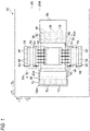
- Fig. 1 is a plan view showing the configuration of the light-emitting device 10 according to the present exemplary embodiment.
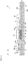
- Fig. 2 is a cross-sectional side view showing the configuration of the light-emitting device 10 according to the present exemplary embodiment.
- a +X direction, a -X direction, a +Y direction, and a -Y direction used in the following description are arrow directions shown in the drawings. Further, the +X direction and the -X direction, and the +Y direction and the -Y direction are directions intersecting with each other (specifically, directions orthogonal to each other).
- the light-emitting device 10 shown in Figs. 1 and 2 is a device that produces light, that is, a device that emits light.
- the light-emitting device 10 includes a substrate 20, a light-emitting element 40, a cathode pattern 30, a drive element 60, a connection pattern 72, and a heat transfer member 80.
- the light-emitting device 10 includes anode patterns 52 and 54, ground patterns 53 and 55, and capacitors 56 and 58.
- the cathode pattern 30, the connection pattern 72, the anode patterns 52 and 54, and the ground patterns 53 and 55 are wiring patterns formed on a front surface 20A of the substrate 20.
- the substrate 20 shown in Figs. 1 and 2 is an example of a "base material". Specifically, the substrate 20 is configured with, for example, a printed substrate having a multilayer structure using an insulator such as a glass epoxy resin. As shown in Fig. 2 , a ground 22 is disposed as an inner layer inside the substrate 20.
- the ground 22 has a reference potential (that is, a reference potential of OV (zero volt)) in a circuit that causes the light-emitting element 40 to operate.
- the ground 22 is an example of a "conductive portion".
- the cathode pattern 30 shown in Figs. 1 and 2 is an example of an "electrode". As shown in Figs. 1 and 2 , the cathode pattern 30 is formed on the front surface 20A of the substrate 20.
- the front surface 20A of the substrate 20 is one surface of the substrate 20. In the present exemplary embodiment, a surface on an upper side in Fig. 2 serves as the front surface 20A.
- the cathode pattern 30 is electrically connected to an electrode of the light-emitting element 40 on a cathode side.
- the cathode pattern 30 is electrically connected to the electrode of the light-emitting element 40 on the cathode side to constitute a part of the electrode of the light-emitting element 40 on the cathode side.
- the light-emitting element 40 is disposed on a front surface 30A of the cathode pattern 30.
- the light-emitting element 40 is a portion that generates light to be emitted to an outside of the light-emitting device 10, and is configured using, for example, a vertical cavity surface emitting laser (VCSEL) in which light-emitting points are arranged in a two-dimensional shape.
- VCSEL vertical cavity surface emitting laser
- the light-emitting element 40 is configured as, for example, a light-emitting unit having a thyristor structure that functions as a switch for selectively turning on and off a light-emitting point.
- the light-emitting element 40 may be configured as a light-emitting unit having no thyristor structure.
- the anode pattern 52 is formed on the front surface 20A of the substrate 20 on a +Y direction side with respect to the light-emitting element 40 and on a +Y direction side with respect to the cathode pattern 30.
- the anode pattern 54 is formed on the front surface 20A of the substrate 20 on a -Y direction side with respect to the light-emitting element 40 and on a -Y direction side with respect to the cathode pattern 30.
- Each of the anode patterns 52 and 54 is electrically connected to the electrode of the light-emitting element 40 on the anode side by wire bonding using plural wires 51.
- the anode patterns 52 and 54 are electrically connected to one terminal of a power supply 50.
- the ground pattern 53 is formed on the front surface 20A of the substrate 20 on the +Y direction side with respect to the anode pattern 52.
- the ground pattern 55 is formed on the front surface 20A of the substrate 20 on the -Y direction side with respect to the anode pattern 54.
- Each of the ground patterns 53 and 55 is electrically connected to the ground 22 by plural vias 57 and 59 penetrating the substrate 20 from the front surface 20A to the ground 22.
- the capacitor 56 is a capacitive element and is provided across the anode pattern 52 and the ground pattern 53.
- the capacitor 56 is electrically connected to each of the anode pattern 52 and the ground pattern 53.
- the capacitor 58 is a capacitive element and is provided across the anode pattern 54 and the ground pattern 55.
- the capacitor 58 is electrically connected to each of the anode pattern 54 and the ground pattern 55. Electric charges are supplied from the power supply 50 to the capacitors 56 and 58 via the anode patterns 52 and 54, and the electric charges are accumulated in the capacitors 56 and 58. Then, the electric charges accumulated in the capacitors 56 and 58 are supplied to the light-emitting element 40.
- the cathode pattern 30 extends to a +X direction side with respect to the light-emitting element 40.
- An end portion of the cathode pattern 30 on a +X direction side serves as a connection portion 36 connected to the drive element 60, as will be described later.
- the drive element 60 is an example of a "drive unit".
- the drive element 60 is an element that drives the light-emitting element 40 to emit light, and is configured with, for example, a semiconductor integrated circuit.
- the drive element 60 is disposed on the +X direction side with respect to the light-emitting element 40, and is electrically connected to the connection portion 36 of the cathode pattern 30 via connection terminals 62.
- the +X direction side is an example of "one direction side along a front surface of the base material".
- a ground pad 18 is formed on the +X direction side with respect to the connection portion 36.
- the ground pad 18 is electrically connected to the ground 22 by plural vias 19 penetrating the substrate 20 from the front surface 20A to the ground 22. Further, the ground pad 18 is connected to a terminal (not shown) for connecting the drive element 60 to the ground 22.
- the cathode pattern 30 extends to the -X direction side with respect to the light-emitting element 40. Therefore, the cathode pattern 30 includes an extension portion 43 extended to the -X direction side with respect to the light-emitting element 40.
- the -X direction side is a direction side opposite to the drive element 60 with respect to the light-emitting element 40.
- the extension portion 43 is disposed on the -X direction side with respect to the anode patterns 52 and 54, and has a width in the -Y direction wider than that of a disposition portion 45 of the cathode pattern 30 where the light-emitting element 40 is disposed.
- the -Y direction is an example of an "intersecting direction intersecting the opposite direction".
- connection structure a structure in which the cathode pattern 30 is thermally connected to the ground 22 (hereinafter, referred to as connection structure) will be described.
- thermally connected refers to connection so as to transfer heat between connection targets.
- connection structure has a function of transferring heat generated in the light-emitting element 40 to the ground 22.
- connection structure includes the connection pattern 72, plural vias 73, and the heat transfer member 80.
- connection pattern 72 is disposed at a position separated from the cathode pattern 30 on the front surface 20A of the substrate 20. Specifically, the connection pattern 72 is disposed on the -X direction side with respect to the extension portion 43 of the cathode pattern 30 with a gap between the connection pattern 72 and the cathode pattern 30.
- the plural vias 73 penetrate from the connection pattern 72 to the ground 22, and electrically and thermally connect the connection pattern 72 and the ground 22. Accordingly, the plural vias 73 transfer heat from the connection pattern 72 to the ground 22.
- the heat transfer member 80 is a member that transfers heat from the cathode pattern 30 to the connection pattern 72.
- the heat transfer member 80 is configured with a high thermal conductivity insulator. Specifically, for example, ceramic such as aluminum nitride is used as the heat transfer member 80. More specifically, the heat transfer member 80 is a member having a thermal conductivity higher than that of the substrate 20. Specifically, the heat transfer member 80 is formed of a material having a thermal conductivity higher than that of the substrate 20.
- the high thermal conductivity refers to a case where the thermal conductivity is 10 [W/mK] or more.
- the insulator refers to a structural body having a volume resistivity of 10 13 [ ⁇ cm] or more.
- the heat transfer member 80 is formed in a block shape (that is, a rectangular parallelepiped shape), and has a contact surface 82 along the front surface 20A of the substrate 20 as shown in Fig. 2 .
- the contact surface 82 is in contact with the front surface 30A of the cathode pattern 30 (specifically, a front surface 43A of the extension portion 43) and a front surface 72A of the connection pattern 72.
- the heat transfer member 80 is disposed from the extension portion 43 toward the -X direction side, and the contact surface 82 is in contact with the connection pattern 72 on the -X direction side with respect to the extension portion 43. Accordingly, the heat transfer member 80 transfers heat from the extension portion 43 of the cathode pattern 30 to the connection pattern 72.
- each of a contact portion 82A with the front surface 30A of the cathode pattern 30 and a contact portion 82B with the front surface 72A of the connection pattern 72 is metalized in an electrically separated state.
- the term "metalized” refers to forming a metal film on a non-metal surface.
- the metal film is formed on a surface of the heat transfer member 80 by, for example, a vapor deposition method such as chemical vapor deposition (CVD) or physical vapor deposition (PVD).
- CVD chemical vapor deposition
- PVD physical vapor deposition
- a metal material such as aluminum or copper is used for the metal film.
- Each of the contact portion 82A and the contact portion 82B is bonded to each of the front surface 30A of the cathode pattern 30 and the front surface 72A of the connection pattern 72 by a bonding material 89 having affinity for metal.
- a bonding material 89 for example, a metal material such as solder or silver paste is used.
- the contact portion 82A In the heat transfer member 80, heat is transferred from the contact portion 82A to the contact portion 82B through the insulator portion, so that the contact portion 82A can be said to be a contact portion in contact with a heat transfer target that takes heat away.
- the contact portion 82B can be said to be a contact portion in contact with a heat transfer object to which heat is transferred.
- the contact portion 82A is an example of a "first contact portion”.
- the contact portion 82B is an example of a "second contact portion”.
- a direction in which the heat transfer member 80 transfers heat from the cathode pattern 30 to the connection pattern 72 is different from a direction in which a current flows between the light-emitting element 40 and the cathode pattern 30.
- the contact surface 82 of the heat transfer member 80 is in contact with the front surface 30A of the cathode pattern 30 and the front surface 72A of the connection pattern 72, and the heat transfer member 80 transfers heat from the cathode pattern 30 to the connection pattern 72 along the contact surface 82. Therefore, in the heat transfer member 80, heat is transferred in the -X direction.
- the light-emitting element 40 is in contact with the front surface 30A of the cathode pattern 30 on a bottom surface 40B, and a current flows in a direction perpendicular to the substrate 20 between the light-emitting element 40 and the cathode pattern 30.
- the heat transfer direction in the heat transfer member 80 is different from the direction in which the current flows between the light-emitting element 40 and the cathode pattern 30.
- the cathode pattern 30 and the connection pattern 72 are thermally connected to each other, but are electrically separated from each other.
- An electrically separated state is a non-conductive state where conduction is not established between separated members and electricity does not flow between the separated members.
- the light-emitting device 10 can be applied to an optical measurement device 100 shown in Fig. 6 .
- the optical measurement device 100 shown in Fig. 6 includes the above-described light-emitting device 10, a light-receiving unit 102, and a processing unit 104.
- a target object 103 is placed so as to face the light-emitting device 10 and the light-receiving unit 102.
- the target object 103 is, for example, a person.
- Fig. 6 is a schematic diagram of the optical measurement device 100 when viewed from above.
- the light-emitting device 10 irradiates the target object 103 with two-dimensionally spread light.
- the light-receiving unit 102 receives reflected light from the target object 103 irradiated with the light from the light-emitting device 10.
- an image-capturing device that receives light from a two-dimensional direction is used.
- the processing unit 104 is configured as, for example, a computer including an input and output unit that inputs and outputs data.
- the processing unit 104 measures a distance from the light-emitting device 10 to the target object 103 or a shape of the target object 103.
- the processing unit 104 operates as follows.
- the processing unit 104 controls the light-emitting device 10 and causes the light-emitting device 10 to emit light in a short period of time. That is, the light-emitting device 10 emits light in a pulsed manner. Then, the processing unit 104 calculates an optical path length from when the light is emitted from the light-emitting device 10 to when the light is reflected by the target object 103 and reaches the light-receiving unit 102, based on a time difference between a point of time when the light-emitting device 10 emits the light and a point of time when the light-receiving unit 102 receives reflected light from the target object 103.
- Positions of the light-emitting device 10 and the light-receiving unit 102 and an interval therebetween are predetermined. Therefore, the processing unit 104 measures a distance from the target object 103 based on a distance from the light-emitting device 10 and the light-receiving unit 102, or a point serving as a reference (hereinafter, referred to as reference point).
- the reference point is a point provided at a predetermined position from the light-emitting device 10 and the light-receiving unit 102.
- the method is a measurement method based on an arrival time of light, and is called a time-of-flight (TOF) method. If the method is performed on plural points on the target object 103, a three-dimensional shape of the target object 103 is measured. As described above, the light from the light-emitting device 10 spreads two-dimensionally and is radiated to the target object 103. Then, reflected light from a portion of the target object 103 having a short distance from the light-emitting device 10 is quickly incident on the light-receiving unit 102. When the above-mentioned image-capturing device that acquires a two-dimensional image is used, a bright spot is recorded in a portion of a frame image where the reflected light reaches.
- TOF time-of-flight
- An optical path length is calculated for each bright spot based on bright spots recorded in a series of frame images. Then, the distance from the light-emitting device 10 and the light-receiving unit 102 or a distance from the reference point is calculated. That is, a three-dimensional shape of the target object 103 is calculated.
- the light-emitting device 10 of the present exemplary embodiment may be used for a light measurement method using a structured light method.
- An optical measurement device to be used is substantially the same as the optical measurement device 100 shown in Fig. 6 using the light-emitting device 10.
- a difference is that a pattern of the light with which the target object 103 is irradiated is an infinite number of light dots (a random pattern), and the light-receiving unit 102 receives the light dots.
- the processing unit 104 processes information on the light.
- the distance to the target object 103 and the three-dimensional shape of the target object 103 are calculated by calculating a positional deviation amount of the infinite number of light dots, instead of obtaining the time difference described above.
- the optical measurement device 100 as described above can be applied to calculation of a distance from an article. Further, the optical measurement device 100 can calculate a shape of the article and can be applied to identification of the article. Then, the optical measurement device 100 can calculate a shape of a face of a person and can be applied to identification (face authentication). Further, the optical measurement device 100 can be applied to detection of an obstacle on a front side, a rear side, a lateral side, or the like by being mounted on a vehicle. As described above, the optical measurement device 100 can be widely used for calculating a distance, a shape, and the like.
- the light-emitting device 10 is not limited to the optical measurement device 100 described above, and can be applied to various devices.
- the light-emitting device 10 may be applied to optical transmission in a combination of the light-emitting device 10, an optical transmission path, and a light-receiving unit, or may be applied to biological detection in which light emitted from the light-emitting device 10 enters an inside of a detection target object, or the like.
- heat generated by the light-emitting element 40 is transferred from the light-emitting element 40 to the cathode pattern 30, the extension portion 43, the heat transfer member 80, the connection pattern 72, the vias 73, and the ground 22 in this order, and is dissipated to the ground 22.
- the heat generated by the light-emitting element 40 is also slightly transferred from the cathode pattern 30 to the substrate 20.
- the heat generated by the light-emitting element 40 is transferred to the ground 22 through the heat transfer member 80, the connection pattern 72, the vias 73, and the like, as compared with a configuration in which heat generated by the light-emitting element 40 is transferred only from the cathode pattern 30 to the substrate 20, the heat from the light-emitting element 40 is efficiently dissipated. Therefore, according to the present exemplary embodiment, a degree of a temperature decreases per unit time in the light-emitting element 40 is increased as compared with the configuration in which the heat generated by the light-emitting element 40 is transferred only from the cathode pattern 30 to the substrate 20. As a result, the light-emitting element 40 can be driven at a high output and a high duty ratio.
- the heat transfer member 80 is configured with an insulator, conduction between the cathode pattern 30 and the connection pattern 72 is prevented as compared with a configuration in which the heat transfer member 80 is a conductor. Accordingly, a state where the cathode pattern 30 and the ground 22 are electrically separated is maintained.
- each of the contact portion 82A with the front surface 30A of the cathode pattern 30 and the contact portion 82B with the front surface 72A of the connection pattern 72 is metalized in the electrically separated state. Therefore, as in the present exemplary embodiment, each of the cathode pattern 30 and the connection pattern 72 can be bonded to the heat transfer member 80 by using the bonding material 89 having affinity for metal.
- the contact surface 82 of the heat transfer member 80 is in contact with the extension portion 43 that extends to the direction side opposite to the drive element 60 with respect to the light-emitting element 40. Therefore, the heat transfer member 80 and the cathode pattern 30 are brought into contact with each other by using a space on the direction side opposite to the drive element 60 with respect to the light-emitting element 40. Therefore, the dead space on the direction side opposite to the drive element 60 with respect to the light-emitting element is effectively used.
- the heat transfer member 80 is disposed from the extension portion 43 toward the -X direction side, and the contact surface 82 is in contact with the connection pattern 72 on the -X direction side with respect to the extension portion 43. Therefore, the heat transfer member 80 and the contact surface 82 are brought into contact with each other by using the space on the -X direction side with respect to the extension portion 43. Therefore, the dead space on the -X direction side with respect to the extension portion 43 is effectively used.
- the extension portion 43 has the width in the -Y direction wider than that of the disposition portion 45 of the cathode pattern 30 where the light-emitting element 40 is disposed. Therefore, as compared with a configuration in which the extension portion 43 has the same width as that of the disposition portion 45, a contact width with the heat transfer member 80 is increased. As a result, the heat from the light-emitting element 40 is efficiently dissipated.
- the contact surface 82 of the heat transfer member 80 is in contact with the front surface 30A of the cathode pattern 30 and the front surface 72A of the connection pattern 72, and the heat transfer member 80 transfers heat from the cathode pattern 30 to the connection pattern 72 along the contact surface 82. Therefore, in the heat transfer member 80, heat is transferred in the -X direction. Therefore, the direction in which the heat transfer member 80 transfers heat from the cathode pattern 30 to the connection pattern 72 is different from the direction in which the current flows between the light-emitting element 40 and the cathode pattern 30.
- the heat transfer member 80 has a thermal conductivity higher than that of the substrate 20. Therefore, as compared with a configuration in which the heat transfer member 80 has the same thermal conductivity as that of the substrate 20, a heat dissipation effect of dissipating the heat of the light-emitting element 40 to the ground 22 is high.
- the heat transfer member 80 in the present exemplary embodiment it is possible to bond each of the heat transfer target and the heat transfer object to the heat transfer member by using the bonding material having affinity for metal while preventing conduction between the cathode pattern 30 that is the heat transfer target and the connection pattern 72 that is the heat transfer object.
- the cathode pattern 30 is used as an example of an electrode, but the present invention is not limited thereto.
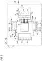
- the electrode as shown in Fig. 3 , for example, the anode pattern 52 may be used.
- a configuration shown in Fig. 3 will be described. Portions having the same functions as those of the configuration shown in Figs. 1 and 2 described above are appropriately denoted by the same reference numerals, and description thereof will be omitted.
- the light-emitting element 40 is disposed on a front surface 52A of the anode pattern 52 formed on the front surface 20A of the substrate 20.
- the anode pattern 52 is electrically connected to an electrode of the light-emitting element 40 on an anode side to constitute a part of the electrode of the light-emitting element 40 on the anode side.
- the ground pattern 53 is formed on the front surface 20A of the substrate 20 on a +Y direction side with respect to the light-emitting element 40 and on the +Y direction side with respect to the anode pattern 52.
- the capacitor 56 is provided across the anode pattern 52 and the ground pattern 53. The capacitor 56 is electrically connected to each of the anode pattern 52 and the ground pattern 53.
- the ground pattern 55 is formed on the front surface 20A of the substrate 20 on the - Y direction side with respect to the light-emitting element 40 and on the -Y direction side with respect to the anode pattern 52.
- the capacitor 58 is provided across the anode pattern 52 and the ground pattern 55.
- the capacitor 58 is electrically connected to each of the anode pattern 52 and the ground pattern 55.
- the cathode pattern 30 is formed on the front surface 20A of the substrate 20 on a +X direction side with respect to the light-emitting element 40 and on the +X direction side with respect to the anode pattern 52.
- the cathode pattern 30 is electrically connected to the electrode of the light-emitting element 40 on the cathode side by wire bonding using the plural wires 51.
- connection portion 36 An end portion of the cathode pattern 30 on the +X direction side serves as the connection portion 36 connected to the drive element 60.
- the drive element 60 is disposed on the +X direction side with respect to the light-emitting element 40, and is electrically connected to the connection portion 36 of the cathode pattern 30 via the connection terminals 62.
- the ground pad 18 is formed on the front surface 20A of the substrate 20 on the +X direction side with respect to the connection portion 36.
- the heat transfer member 80 is in contact with the front surface 52A of the anode pattern 52 and the front surface 72A of the connection pattern 72. Accordingly, the heat transfer member 80 transfers heat from the anode pattern 52 to the connection pattern 72.
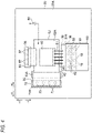
- the anode pattern 52 as shown in Fig. 4 may be used as an example of an electrode.
- a configuration shown in Fig. 4 will be described. Portions having the same functions as those of the configuration shown in Figs. 1 and 2 described above are appropriately denoted by the same reference numerals, and description thereof will be omitted.
- the light-emitting element 40 is disposed on the front surface 52A of the anode pattern 52 formed on the front surface 20A of the substrate 20.
- the anode pattern 52 is electrically connected to an electrode of the light-emitting element 40 on an anode side to constitute a part of the electrode of the light-emitting element 40 on the anode side.
- the ground pattern 53 is formed on the front surface 20A of the substrate 20 on a +Y direction side with respect to the light-emitting element 40 and on the +Y direction side with respect to the anode pattern 52.
- the capacitor 56 is provided across the anode pattern 52 and the ground pattern 53. The capacitor 56 is electrically connected to each of the anode pattern 52 and the ground pattern 53.
- the cathode pattern 30 is formed on the front surface 20A of the substrate 20 on a - Y direction side with respect to the light-emitting element 40 and on the -Y direction side with respect to the anode pattern 52.
- the cathode pattern 30 is electrically connected to the electrode of the light-emitting element 40 on the cathode side by wire bonding using the plural wires 51.
- An end portion of the cathode pattern 30 on the -Y direction side serves as the connection portion 36 connected to the drive element 60.
- the drive element 60 is disposed on the -Y direction side with respect to the light-emitting element 40, and is electrically connected to the connection portion 36 of the cathode pattern 30 via the connection terminals 62.
- the ground pad 18 is formed on the front surface 20A of the substrate 20 on the -Y direction side with respect to the connection portion 36.
- the anode pattern 52 extends to a -X direction side with respect to the light-emitting element 40. Therefore, the anode pattern 52 includes the extension portion 43 extended to the -X direction side with respect to the light-emitting element 40. Specifically, the extension portion 43 is disposed on the -X direction side with respect to the cathode pattern 30, and has a width in the -Y direction wider than that of the disposition portion 45 of the anode pattern 52 where the light-emitting element 40 is disposed. Then, the heat transfer member 80 is in contact with the front surface 43A of the extension portion 43 of the anode pattern 52 and the front surface 72A of the connection pattern 72. Accordingly, the heat transfer member 80 transfers heat from the extension portion 43 of the anode pattern 52 to the connection pattern 72.
- the heat transfer member 80 may be disposed between the cathode pattern 30 and the ground 22.
- the heat transfer member 80 is referred to as a heat transfer member 80 (X) in order to distinguish the heat transfer member 80 from the above-described heat transfer member 80. Further, description of the same portions as those of the above-described heat transfer member 80 will be appropriately omitted.
- the heat transfer member 80 (X) is disposed between the cathode pattern 30 and the ground 22 at a position on a lower side with respect to the light-emitting element 40.
- the heat transfer member 80 (X) includes contact surfaces 82 and 84 along the front surface 20A of the substrate 20. Specifically, one surface (specifically, an upper surface in Fig. 5 ) of the heat transfer member 80 (X) serves as the contact surface 82, and the other surface (specifically, a lower surface in Fig. 5 ) of the heat transfer member 80 (X) serves as the contact surface 84.
- Each of the contact surface 82 and the contact surface 84 is in contact with a back surface 30B of the cathode pattern 30 and a front surface 22A of the ground 22. Accordingly, the heat transfer member 80 (X) transfers heat from the cathode pattern 30 to the ground 22. In this case, heat is transferred from the cathode pattern 30 to the ground 22 without passing through the connection pattern 72 and the vias 73. Further, in this case, the heat transfer member 80 (X) transfers heat in a direction perpendicular to the substrate 20. Therefore, both the heat transfer direction in the heat transfer member 80 and a direction in which a current flows between the light-emitting element 40 and the cathode pattern 30 are perpendicular to the substrate 20.
- each of the contact surface 82 and the contact surface 84 is metalized in an electrically separated state.
- the heat is transferred from the contact surface 82 to the contact surface 84 through an insulator portion, so that the contact surface 82 can be said to be a contact portion in contact with a heat transfer target that takes the heat away.
- the contact surface 84B can be said to be a contact portion in contact with a heat transfer object that transfers the heat.
- the contact surface 82 is an example of a "first contact portion”.
- the contact surface 84 is an example of a "second contact portion”.
- the substrate 20 is used as an example of a base material, but the present invention is not limited thereto.
- a heat dissipation member that is provided on the front surface 20A of the substrate 20 and has a thermal conductivity higher than that of the substrate 20 may be used, or a member other than the substrate 20 may be used.
- the heat transfer member 80 is configured with the insulator, but the present invention is not limited thereto.
- the heat transfer member 80 may be a conductor.
- an insulator is used in at least one of the connection pattern 72 and the vias 73, and a state where the cathode pattern 30 and the ground 22 are electrically separated is maintained.
- each of the contact portion 82A with the front surface 30A of the cathode pattern 30 and the contact portion 82B with the front surface 72A of the connection pattern 72 is metalized in an electrically separated state.
- the present invention is not limited thereto, the heat transfer member 80 including the not processed contact surface 82 may be used.
- the heat transfer member 80 is in contact with the connection pattern 72 formed on the front surface 20A of the substrate 20, but the present invention is not limited thereto.
- the connection pattern 72 may not be formed on the front surface 20A of the substrate 20, and the heat transfer member 80 may be in direct contact with the vias 73, or may be in contact with a member that transfers heat to the ground 22.
- the via 73 functions as an example of a "connection portion".
- the extension portion 43 extends to the direction side opposite to the drive element 60 with respect to the light-emitting element 40, but the present invention is not limited thereto.
- the extension portion 43 may be configured to, for example, be extended in the +Y direction or the -Y direction.
- the extension portion 43 has the width in the -Y direction wider than that of the disposition portion 45 of the cathode pattern 30 where the light-emitting element 40 is disposed, but the present invention is not limited thereto.
- the extension portion 43 may have the same width as that of the disposition portion 45.
- the direction in which the heat transfer member 80 transfers heat from the cathode pattern 30 to the connection pattern 72 is different from the direction in which the current flows between the light-emitting element 40 and the cathode pattern 30, but the present invention is not limited thereto.
- the direction in which the heat transfer member 80 transfers heat from the cathode pattern 30 to the connection pattern 72 may be the same as the direction in which the current flows between the light-emitting element 40 and the cathode pattern 30 (see Fig. 5 ).
- the ground 22 is disposed inside the substrate 20 as the inner layer, but the present invention is not limited thereto.
- the ground 22 may be disposed on a back surface 20B of the substrate 20 (that is, a surface on a side opposite to the front surface 20A).
Landscapes
- Physics & Mathematics (AREA)
- General Physics & Mathematics (AREA)
- Condensed Matter Physics & Semiconductors (AREA)
- Electromagnetism (AREA)
- Optics & Photonics (AREA)
- Engineering & Computer Science (AREA)
- Computer Networks & Wireless Communication (AREA)
- Radar, Positioning & Navigation (AREA)
- Remote Sensing (AREA)
- Led Device Packages (AREA)
- Length Measuring Devices By Optical Means (AREA)
- Semiconductor Lasers (AREA)
Abstract
Description
- The present invention relates to a light-emitting device, a heat transfer member, and an optical measurement device.
- Patent Literature 1 discloses a chip shape heat generation component including an electrode for heat dissipation provided to dissipate heat generated by a main body portion in a chip component for surface mounting including the main body portion having a function as a circuit element and an electrode serving as both an electrical connection and a mechanical connection.
- Patent Literature 2 discloses a heat transfer method for heat dissipation of an electrical component, in which in an electrical wiring printed substrate on which the electrical component is mounted, an optional heat conductor for transferring heat generated by the electrical component is continuously disposed on optional wiring on the substrate.
-
- [Patent Literature 1]:
JP-A-H6-169189 - [Patent Literature 2]:
JP-A-H10-84175 - As a light-emitting device, a light-emitting device that includes a base material such as a printed substrate, an electrode disposed on a front surface of the base material, and a light-emitting element disposed on a front surface of the electrode, and in which the electrode is electrically connected to the light-emitting element, may be considered. In the light-emitting device, when heat generated by the light-emitting element is transferred only from the electrode to the base material, the heat of the light-emitting element may not be efficiently dissipated.
- An object of the present invention is to efficiently dissipate the heat of the light-emitting element as compared with a configuration in which heat generated by a light-emitting element is transferred only from an electrode to a base material.
- According to a first aspect of the present disclosure, there is provided a light-emitting device including: a base material; an electrode that is disposed on a front surface of the base material, that has a light-emitting element on a front surface of the electrode, and that is electrically connected to the light-emitting element; a connection portion disposed at a position separated from the electrode on the front surface of the base material and connected to a conductive portion having a reference potential; and a heat transfer member that includes a contact surface along the front surface of the base material, the contact surface being in contact with a front surface of the electrode and a front surface of the connection portion, the heating transfer member being configured to transfer heat from the electrode to the connection portion.
- In a second aspect, the heat transfer member is an insulator.
- In a third aspect, a contact portion on the contact surface of the heat transfer member that is in contact with the front surface of the electrode and a contact portion on the contact surface of the heat transfer member that is in contact with the front surface of the connection portion are metalized in an electrically separated state from each other.
- In a fourth aspect, the light-emitting device further includes a drive unit disposed on one direction side along the front surface of the base material with respect to the light-emitting element and configured to drive the light-emitting element, in which the electrode extends from the light-emitting element to a direction side opposite to the drive unit with respect to the light-emitting element, and in which the contact surface is in contact with an extension portion of the electrode.
- In a fifth aspect, the connection portion is disposed on the opposite direction side with respect to the extension portion, and the heat transfer member is disposed from the extension portion toward the opposite direction side, and the contact surface is in contact with the connection portion on the opposite direction side with respect to the extension portion.
- In a sixth aspect, a width of the extension portion in an intersecting direction that intersects the opposite direction is wider than a width in the intersecting direction of the electrode where the light-emitting element is disposed.
- In a seventh aspect, a direction in which the heat transfer member transfers heat from the electrode to the connection portion is different from a direction in which a current flows between the light-emitting element and the electrode.
- In an eighth aspect, a thermal conductivity of the heat transfer member is higher than a thermal conductivity of the base material.
- A ninth aspect provides a light-emitting device including a base material; an electrode that is disposed on a front surface of the base material, that has a light-emitting element on a front surface of the electrode, and that is electrically connected to the light-emitting element; a connection portion disposed at a position separated from the electrode on the front surface of the base material and connected to a conductive portion having a reference potential; and a heat transfer member that is configured with an insulator, that is in contact with a front surface of the electrode and a front surface of the connection portion, and that is configured to transfer heat from the electrode to the connection portion.
- A tenth aspect provides a heat transfer member including: a first contact portion in contact with a heat transfer target from which heat is taken away; and a second contact portion in contact with a heat transfer object to which the heat is transferred, in which the heat transfer member is configured with an insulator having a high thermal conductivity, and in which the first contact portion and the second contact portion are metalized in an electrically separated state from each other.
- An eleventh aspect provides an optical measurement device including: the light-emitting device according to any one of aspects 1 to 9; a light-receiving unit configured to receive reflected light from a target object irradiated with light from the light-emitting device; and a processing unit configured to process information on light received by the light-receiving unit to measure a distance from the light-emitting device to the target object or a shape of the target object.
- According to the configuration of the first aspect, heat of the light-emitting element can be efficiently dissipated as compared with a configuration in which heat generated by a light-emitting element is transferred only from an electrode to a base material.
- According to the configuration of the second aspect, conduction between the electrode and the connection portion is prevented as compared with a configuration in which a heat transfer member is a conductor.
- According to the configuration of the third aspect, each of the electrode and the connection portion can be bonded to the heat transfer member by using the bonding material having affinity for metal.
- According to the configuration of the fourth aspect, the heat transfer member and the electrode can be brought into contact with each other by using the space on the direction side opposite to the drive unit with respect to the light-emitting element.
- According to the configuration of the fifth aspect, the heat transfer member and the connection portion can be brought into contact with each other by using the space on the direction side opposite to the extension portion of the electrode.
- According to the configuration of the sixth aspect, a contact width with the heat transfer member can be increased as compared with a configuration in which an extension portion of an electrode has the same width as that of a portion where a light-emitting element is disposed.
- According to the configuration of the seventh aspect, as compared with a configuration in which a direction in which a heat transfer member transfers heat from an electrode to a connection portion is the same as a direction in which a current flows between a light-emitting element and the electrode, heat can be dissipated at a position that does not influence a current path.
- According to the configuration of the eighth aspect, as compared with a configuration in which a heat transfer member has the same thermal conductivity as that of a base material, a heat dissipation effect of dissipating the heat of the light-emitting element to a conductive portion is high.
- According to the configuration of the ninth aspect, the heat of the light-emitting element can be efficiently dissipated as compared with the configuration in which the heat generated by the light-emitting element is transferred only from the electrode to the base material.
- According to the configuration of the tenth aspect, each of the heat transfer target and the heat transfer obj ect can be bonded to the heat transfer member by using the bonding material having affinity for metal while preventing conduction between the heat transfer target and the heat transfer object.
- According to the configuration of the eleventh aspect, as compared with a configuration including a light-emitting device in which heat generated by the light-emitting element is transferred only from an electrode to a base material, heat of the light-emitting element in the light-emitting device can be efficiently dissipated.
- Exemplary embodiment(s) of the present invention will be described in detail based on the following figures, wherein:
-
Fig. 1 is a plan view showing a configuration of a light-emitting device according to the present exemplary embodiment; -
Fig. 2 is a cross-sectional side view showing the configuration of the light-emitting device according to the present exemplary embodiment; -
Fig. 3 is a plan view showing a configuration of a light-emitting device according to a first modified example; -
Fig. 4 is a plan view showing a configuration of a light-emitting device according to a second modified example; -
Fig. 5 is a cross-sectional side view showing another application example of a heat transfer member; and -
Fig. 6 is a schematic diagram showing a configuration of an optical measurement device to which the light-emitting device according to the present exemplary embodiment is applied. - Hereinafter, an example of an exemplary embodiment according to the present invention will be described with reference to the drawings.
- First, a configuration of a light-emitting
device 10 according to the present exemplary embodiment will be described.Fig. 1 is a plan view showing the configuration of the light-emitting device 10 according to the present exemplary embodiment.Fig. 2 is a cross-sectional side view showing the configuration of the light-emitting device 10 according to the present exemplary embodiment. - A +X direction, a -X direction, a +Y direction, and a -Y direction used in the following description are arrow directions shown in the drawings. Further, the +X direction and the -X direction, and the +Y direction and the -Y direction are directions intersecting with each other (specifically, directions orthogonal to each other).
- The light-
emitting device 10 shown inFigs. 1 and2 is a device that produces light, that is, a device that emits light. Specifically, as shown inFigs. 1 and2 , the light-emitting device 10 includes asubstrate 20, a light-emitting element 40, acathode pattern 30, adrive element 60, aconnection pattern 72, and aheat transfer member 80. Further, as shown inFig. 1 , the light-emitting device 10 includesanode patterns ground patterns capacitors cathode pattern 30, theconnection pattern 72, theanode patterns ground patterns front surface 20A of thesubstrate 20. - The
substrate 20 shown inFigs. 1 and2 is an example of a "base material". Specifically, thesubstrate 20 is configured with, for example, a printed substrate having a multilayer structure using an insulator such as a glass epoxy resin. As shown inFig. 2 , aground 22 is disposed as an inner layer inside thesubstrate 20. Theground 22 has a reference potential (that is, a reference potential of OV (zero volt)) in a circuit that causes the light-emittingelement 40 to operate. Theground 22 is an example of a "conductive portion". - The
cathode pattern 30 shown inFigs. 1 and2 is an example of an "electrode". As shown inFigs. 1 and2 , thecathode pattern 30 is formed on thefront surface 20A of thesubstrate 20. Thefront surface 20A of thesubstrate 20 is one surface of thesubstrate 20. In the present exemplary embodiment, a surface on an upper side inFig. 2 serves as thefront surface 20A. - Further, the
cathode pattern 30 is electrically connected to an electrode of the light-emittingelement 40 on a cathode side. Thecathode pattern 30 is electrically connected to the electrode of the light-emittingelement 40 on the cathode side to constitute a part of the electrode of the light-emittingelement 40 on the cathode side. - As shown in
Figs. 1 and2 , the light-emittingelement 40 is disposed on afront surface 30A of thecathode pattern 30. The light-emittingelement 40 is a portion that generates light to be emitted to an outside of the light-emittingdevice 10, and is configured using, for example, a vertical cavity surface emitting laser (VCSEL) in which light-emitting points are arranged in a two-dimensional shape. Further, the light-emittingelement 40 is configured as, for example, a light-emitting unit having a thyristor structure that functions as a switch for selectively turning on and off a light-emitting point. The light-emittingelement 40 may be configured as a light-emitting unit having no thyristor structure. - As shown in
Fig. 1 , theanode pattern 52 is formed on thefront surface 20A of thesubstrate 20 on a +Y direction side with respect to the light-emittingelement 40 and on a +Y direction side with respect to thecathode pattern 30. Theanode pattern 54 is formed on thefront surface 20A of thesubstrate 20 on a -Y direction side with respect to the light-emittingelement 40 and on a -Y direction side with respect to thecathode pattern 30. Each of theanode patterns element 40 on the anode side by wire bonding usingplural wires 51. Theanode patterns power supply 50. - The
ground pattern 53 is formed on thefront surface 20A of thesubstrate 20 on the +Y direction side with respect to theanode pattern 52. Theground pattern 55 is formed on thefront surface 20A of thesubstrate 20 on the -Y direction side with respect to theanode pattern 54. Each of theground patterns ground 22 byplural vias substrate 20 from thefront surface 20A to theground 22. - The
capacitor 56 is a capacitive element and is provided across theanode pattern 52 and theground pattern 53. Thecapacitor 56 is electrically connected to each of theanode pattern 52 and theground pattern 53. - The
capacitor 58 is a capacitive element and is provided across theanode pattern 54 and theground pattern 55. Thecapacitor 58 is electrically connected to each of theanode pattern 54 and theground pattern 55. Electric charges are supplied from thepower supply 50 to thecapacitors anode patterns capacitors capacitors element 40. - The
cathode pattern 30 extends to a +X direction side with respect to the light-emittingelement 40. An end portion of thecathode pattern 30 on a +X direction side serves as aconnection portion 36 connected to thedrive element 60, as will be described later. - The
drive element 60 is an example of a "drive unit". Thedrive element 60 is an element that drives the light-emittingelement 40 to emit light, and is configured with, for example, a semiconductor integrated circuit. In the present exemplary embodiment, thedrive element 60 is disposed on the +X direction side with respect to the light-emittingelement 40, and is electrically connected to theconnection portion 36 of thecathode pattern 30 viaconnection terminals 62. The +X direction side is an example of "one direction side along a front surface of the base material". - On the
front surface 20A of thesubstrate 20, aground pad 18 is formed on the +X direction side with respect to theconnection portion 36. Theground pad 18 is electrically connected to theground 22 byplural vias 19 penetrating thesubstrate 20 from thefront surface 20A to theground 22. Further, theground pad 18 is connected to a terminal (not shown) for connecting thedrive element 60 to theground 22. - The
cathode pattern 30 extends to the -X direction side with respect to the light-emittingelement 40. Therefore, thecathode pattern 30 includes anextension portion 43 extended to the -X direction side with respect to the light-emittingelement 40. The -X direction side is a direction side opposite to thedrive element 60 with respect to the light-emittingelement 40. - Specifically, the
extension portion 43 is disposed on the -X direction side with respect to theanode patterns disposition portion 45 of thecathode pattern 30 where the light-emittingelement 40 is disposed. The -Y direction is an example of an "intersecting direction intersecting the opposite direction". - Here, a structure in which the
cathode pattern 30 is thermally connected to the ground 22 (hereinafter, referred to as connection structure) will be described. The term "thermally connected" refers to connection so as to transfer heat between connection targets. - The connection structure has a function of transferring heat generated in the light-emitting
element 40 to theground 22. Specifically, in the present exemplary embodiment, the connection structure includes theconnection pattern 72,plural vias 73, and theheat transfer member 80. - As shown in
Figs. 1 and2 , theconnection pattern 72 is disposed at a position separated from thecathode pattern 30 on thefront surface 20A of thesubstrate 20. Specifically, theconnection pattern 72 is disposed on the -X direction side with respect to theextension portion 43 of thecathode pattern 30 with a gap between theconnection pattern 72 and thecathode pattern 30. Theplural vias 73 penetrate from theconnection pattern 72 to theground 22, and electrically and thermally connect theconnection pattern 72 and theground 22. Accordingly, theplural vias 73 transfer heat from theconnection pattern 72 to theground 22. - The
heat transfer member 80 is a member that transfers heat from thecathode pattern 30 to theconnection pattern 72. Theheat transfer member 80 is configured with a high thermal conductivity insulator. Specifically, for example, ceramic such as aluminum nitride is used as theheat transfer member 80. More specifically, theheat transfer member 80 is a member having a thermal conductivity higher than that of thesubstrate 20. Specifically, theheat transfer member 80 is formed of a material having a thermal conductivity higher than that of thesubstrate 20. In the present exemplary embodiment, the high thermal conductivity refers to a case where the thermal conductivity is 10 [W/mK] or more. Further, in the present exemplary embodiment, the insulator refers to a structural body having a volume resistivity of 1013 [Ω·cm] or more. - Further, the
heat transfer member 80 is formed in a block shape (that is, a rectangular parallelepiped shape), and has acontact surface 82 along thefront surface 20A of thesubstrate 20 as shown inFig. 2 . Thecontact surface 82 is in contact with thefront surface 30A of the cathode pattern 30 (specifically, afront surface 43A of the extension portion 43) and afront surface 72A of theconnection pattern 72. Specifically, theheat transfer member 80 is disposed from theextension portion 43 toward the -X direction side, and thecontact surface 82 is in contact with theconnection pattern 72 on the -X direction side with respect to theextension portion 43. Accordingly, theheat transfer member 80 transfers heat from theextension portion 43 of thecathode pattern 30 to theconnection pattern 72. - In the
contact surface 82 of theheat transfer member 80, each of acontact portion 82A with thefront surface 30A of thecathode pattern 30 and acontact portion 82B with thefront surface 72A of theconnection pattern 72 is metalized in an electrically separated state. Here, the term "metalized" refers to forming a metal film on a non-metal surface. Specifically, the metal film is formed on a surface of theheat transfer member 80 by, for example, a vapor deposition method such as chemical vapor deposition (CVD) or physical vapor deposition (PVD). As an example, a metal material such as aluminum or copper is used for the metal film. Each of thecontact portion 82A and thecontact portion 82B is bonded to each of thefront surface 30A of thecathode pattern 30 and thefront surface 72A of theconnection pattern 72 by abonding material 89 having affinity for metal. As thebonding material 89, for example, a metal material such as solder or silver paste is used. - In the
heat transfer member 80, heat is transferred from thecontact portion 82A to thecontact portion 82B through the insulator portion, so that thecontact portion 82A can be said to be a contact portion in contact with a heat transfer target that takes heat away. On the other hand, thecontact portion 82B can be said to be a contact portion in contact with a heat transfer object to which heat is transferred. Thecontact portion 82A is an example of a "first contact portion". Thecontact portion 82B is an example of a "second contact portion". - In the present exemplary embodiment, a direction in which the
heat transfer member 80 transfers heat from thecathode pattern 30 to theconnection pattern 72 is different from a direction in which a current flows between the light-emittingelement 40 and thecathode pattern 30. Specifically, thecontact surface 82 of theheat transfer member 80 is in contact with thefront surface 30A of thecathode pattern 30 and thefront surface 72A of theconnection pattern 72, and theheat transfer member 80 transfers heat from thecathode pattern 30 to theconnection pattern 72 along thecontact surface 82. Therefore, in theheat transfer member 80, heat is transferred in the -X direction. The light-emittingelement 40 is in contact with thefront surface 30A of thecathode pattern 30 on abottom surface 40B, and a current flows in a direction perpendicular to thesubstrate 20 between the light-emittingelement 40 and thecathode pattern 30. As described above, in the present exemplary embodiment, the heat transfer direction in theheat transfer member 80 is different from the direction in which the current flows between the light-emittingelement 40 and thecathode pattern 30. - As described above, since the
heat transfer member 80 is configured with the high thermal conductivity insulator, thecathode pattern 30 and theconnection pattern 72 are thermally connected to each other, but are electrically separated from each other. An electrically separated state is a non-conductive state where conduction is not established between separated members and electricity does not flow between the separated members. - As an example, the light-emitting
device 10 can be applied to anoptical measurement device 100 shown inFig. 6 . Theoptical measurement device 100 shown inFig. 6 includes the above-described light-emittingdevice 10, a light-receivingunit 102, and aprocessing unit 104. In theoptical measurement device 100, atarget object 103 is placed so as to face the light-emittingdevice 10 and the light-receivingunit 102. InFig. 6 , thetarget object 103 is, for example, a person. Further,Fig. 6 is a schematic diagram of theoptical measurement device 100 when viewed from above. - As an example, as indicated by a solid line in
Fig. 6 , the light-emittingdevice 10 irradiates thetarget object 103 with two-dimensionally spread light. As indicated by a broken line inFig. 6 , the light-receivingunit 102 receives reflected light from thetarget object 103 irradiated with the light from the light-emittingdevice 10. As the light-receivingunit 102, for example, an image-capturing device that receives light from a two-dimensional direction is used. - The
processing unit 104 is configured as, for example, a computer including an input and output unit that inputs and outputs data. Theprocessing unit 104 measures a distance from the light-emittingdevice 10 to thetarget object 103 or a shape of thetarget object 103. Specifically, theprocessing unit 104 operates as follows. - The
processing unit 104 controls the light-emittingdevice 10 and causes the light-emittingdevice 10 to emit light in a short period of time. That is, the light-emittingdevice 10 emits light in a pulsed manner. Then, theprocessing unit 104 calculates an optical path length from when the light is emitted from the light-emittingdevice 10 to when the light is reflected by thetarget object 103 and reaches the light-receivingunit 102, based on a time difference between a point of time when the light-emittingdevice 10 emits the light and a point of time when the light-receivingunit 102 receives reflected light from thetarget object 103. Positions of the light-emittingdevice 10 and the light-receivingunit 102 and an interval therebetween are predetermined. Therefore, theprocessing unit 104 measures a distance from thetarget object 103 based on a distance from the light-emittingdevice 10 and the light-receivingunit 102, or a point serving as a reference (hereinafter, referred to as reference point). The reference point is a point provided at a predetermined position from the light-emittingdevice 10 and the light-receivingunit 102. - The method is a measurement method based on an arrival time of light, and is called a time-of-flight (TOF) method. If the method is performed on plural points on the
target object 103, a three-dimensional shape of thetarget object 103 is measured. As described above, the light from the light-emittingdevice 10 spreads two-dimensionally and is radiated to thetarget object 103. Then, reflected light from a portion of thetarget object 103 having a short distance from the light-emittingdevice 10 is quickly incident on the light-receivingunit 102. When the above-mentioned image-capturing device that acquires a two-dimensional image is used, a bright spot is recorded in a portion of a frame image where the reflected light reaches. An optical path length is calculated for each bright spot based on bright spots recorded in a series of frame images. Then, the distance from the light-emittingdevice 10 and the light-receivingunit 102 or a distance from the reference point is calculated. That is, a three-dimensional shape of thetarget object 103 is calculated. - As another method, the light-emitting
device 10 of the present exemplary embodiment may be used for a light measurement method using a structured light method. An optical measurement device to be used is substantially the same as theoptical measurement device 100 shown inFig. 6 using the light-emittingdevice 10. A difference is that a pattern of the light with which thetarget object 103 is irradiated is an infinite number of light dots (a random pattern), and the light-receivingunit 102 receives the light dots. Then, theprocessing unit 104 processes information on the light. Here, as a method of processing, the distance to thetarget object 103 and the three-dimensional shape of thetarget object 103 are calculated by calculating a positional deviation amount of the infinite number of light dots, instead of obtaining the time difference described above. - The
optical measurement device 100 as described above can be applied to calculation of a distance from an article. Further, theoptical measurement device 100 can calculate a shape of the article and can be applied to identification of the article. Then, theoptical measurement device 100 can calculate a shape of a face of a person and can be applied to identification (face authentication). Further, theoptical measurement device 100 can be applied to detection of an obstacle on a front side, a rear side, a lateral side, or the like by being mounted on a vehicle. As described above, theoptical measurement device 100 can be widely used for calculating a distance, a shape, and the like. - The light-emitting
device 10 is not limited to theoptical measurement device 100 described above, and can be applied to various devices. For example, the light-emittingdevice 10 may be applied to optical transmission in a combination of the light-emittingdevice 10, an optical transmission path, and a light-receiving unit, or may be applied to biological detection in which light emitted from the light-emittingdevice 10 enters an inside of a detection target object, or the like. - In the present exemplary embodiment, heat generated by the light-emitting
element 40 is transferred from the light-emittingelement 40 to thecathode pattern 30, theextension portion 43, theheat transfer member 80, theconnection pattern 72, thevias 73, and theground 22 in this order, and is dissipated to theground 22. The heat generated by the light-emittingelement 40 is also slightly transferred from thecathode pattern 30 to thesubstrate 20. - As described above, in the present exemplary embodiment, since the heat generated by the light-emitting
element 40 is transferred to theground 22 through theheat transfer member 80, theconnection pattern 72, thevias 73, and the like, as compared with a configuration in which heat generated by the light-emittingelement 40 is transferred only from thecathode pattern 30 to thesubstrate 20, the heat from the light-emittingelement 40 is efficiently dissipated. Therefore, according to the present exemplary embodiment, a degree of a temperature decreases per unit time in the light-emittingelement 40 is increased as compared with the configuration in which the heat generated by the light-emittingelement 40 is transferred only from thecathode pattern 30 to thesubstrate 20. As a result, the light-emittingelement 40 can be driven at a high output and a high duty ratio. - In the present exemplary embodiment, since the
heat transfer member 80 is configured with an insulator, conduction between thecathode pattern 30 and theconnection pattern 72 is prevented as compared with a configuration in which theheat transfer member 80 is a conductor. Accordingly, a state where thecathode pattern 30 and theground 22 are electrically separated is maintained. - In the present exemplary embodiment, in the
contact surface 82 of theheat transfer member 80, each of thecontact portion 82A with thefront surface 30A of thecathode pattern 30 and thecontact portion 82B with thefront surface 72A of theconnection pattern 72 is metalized in the electrically separated state. Therefore, as in the present exemplary embodiment, each of thecathode pattern 30 and theconnection pattern 72 can be bonded to theheat transfer member 80 by using thebonding material 89 having affinity for metal. - In the present exemplary embodiment, the
contact surface 82 of theheat transfer member 80 is in contact with theextension portion 43 that extends to the direction side opposite to thedrive element 60 with respect to the light-emittingelement 40. Therefore, theheat transfer member 80 and thecathode pattern 30 are brought into contact with each other by using a space on the direction side opposite to thedrive element 60 with respect to the light-emittingelement 40. Therefore, the dead space on the direction side opposite to thedrive element 60 with respect to the light-emitting element is effectively used. - In the present exemplary embodiment, the
heat transfer member 80 is disposed from theextension portion 43 toward the -X direction side, and thecontact surface 82 is in contact with theconnection pattern 72 on the -X direction side with respect to theextension portion 43. Therefore, theheat transfer member 80 and thecontact surface 82 are brought into contact with each other by using the space on the -X direction side with respect to theextension portion 43. Therefore, the dead space on the -X direction side with respect to theextension portion 43 is effectively used. - In the present exemplary embodiment, the
extension portion 43 has the width in the -Y direction wider than that of thedisposition portion 45 of thecathode pattern 30 where the light-emittingelement 40 is disposed. Therefore, as compared with a configuration in which theextension portion 43 has the same width as that of thedisposition portion 45, a contact width with theheat transfer member 80 is increased. As a result, the heat from the light-emittingelement 40 is efficiently dissipated. - In the present exemplary embodiment, the
contact surface 82 of theheat transfer member 80 is in contact with thefront surface 30A of thecathode pattern 30 and thefront surface 72A of theconnection pattern 72, and theheat transfer member 80 transfers heat from thecathode pattern 30 to theconnection pattern 72 along thecontact surface 82. Therefore, in theheat transfer member 80, heat is transferred in the -X direction. Therefore, the direction in which theheat transfer member 80 transfers heat from thecathode pattern 30 to theconnection pattern 72 is different from the direction in which the current flows between the light-emittingelement 40 and thecathode pattern 30. Therefore, as compared with a configuration in which a direction in which theheat transfer member 80 transfers heat from thecathode pattern 30 to theconnection pattern 72 is the same as a direction in which a current flows between the light-emittingelement 40 and thecathode pattern 30, it is possible to dissipate heat at a position that does not influence a current path. - In the present exemplary embodiment, the
heat transfer member 80 has a thermal conductivity higher than that of thesubstrate 20. Therefore, as compared with a configuration in which theheat transfer member 80 has the same thermal conductivity as that of thesubstrate 20, a heat dissipation effect of dissipating the heat of the light-emittingelement 40 to theground 22 is high. - According to the
heat transfer member 80 in the present exemplary embodiment, it is possible to bond each of the heat transfer target and the heat transfer object to the heat transfer member by using the bonding material having affinity for metal while preventing conduction between thecathode pattern 30 that is the heat transfer target and theconnection pattern 72 that is the heat transfer object. - In the present exemplary embodiment, the
cathode pattern 30 is used as an example of an electrode, but the present invention is not limited thereto. As an example of the electrode, as shown inFig. 3 , for example, theanode pattern 52 may be used. Hereinafter, a configuration shown inFig. 3 will be described. Portions having the same functions as those of the configuration shown inFigs. 1 and2 described above are appropriately denoted by the same reference numerals, and description thereof will be omitted. - In the configuration shown in
Fig. 3 , the light-emittingelement 40 is disposed on afront surface 52A of theanode pattern 52 formed on thefront surface 20A of thesubstrate 20. Theanode pattern 52 is electrically connected to an electrode of the light-emittingelement 40 on an anode side to constitute a part of the electrode of the light-emittingelement 40 on the anode side. - The
ground pattern 53 is formed on thefront surface 20A of thesubstrate 20 on a +Y direction side with respect to the light-emittingelement 40 and on the +Y direction side with respect to theanode pattern 52. Thecapacitor 56 is provided across theanode pattern 52 and theground pattern 53. Thecapacitor 56 is electrically connected to each of theanode pattern 52 and theground pattern 53. - The
ground pattern 55 is formed on thefront surface 20A of thesubstrate 20 on the - Y direction side with respect to the light-emittingelement 40 and on the -Y direction side with respect to theanode pattern 52. Thecapacitor 58 is provided across theanode pattern 52 and theground pattern 55. Thecapacitor 58 is electrically connected to each of theanode pattern 52 and theground pattern 55. - The
cathode pattern 30 is formed on thefront surface 20A of thesubstrate 20 on a +X direction side with respect to the light-emittingelement 40 and on the +X direction side with respect to theanode pattern 52. Thecathode pattern 30 is electrically connected to the electrode of the light-emittingelement 40 on the cathode side by wire bonding using theplural wires 51. - An end portion of the
cathode pattern 30 on the +X direction side serves as theconnection portion 36 connected to thedrive element 60. Thedrive element 60 is disposed on the +X direction side with respect to the light-emittingelement 40, and is electrically connected to theconnection portion 36 of thecathode pattern 30 via theconnection terminals 62. Theground pad 18 is formed on thefront surface 20A of thesubstrate 20 on the +X direction side with respect to theconnection portion 36. - In the configuration shown in
Fig. 3 , theheat transfer member 80 is in contact with thefront surface 52A of theanode pattern 52 and thefront surface 72A of theconnection pattern 72. Accordingly, theheat transfer member 80 transfers heat from theanode pattern 52 to theconnection pattern 72. - As an example of an electrode, the
anode pattern 52 as shown inFig. 4 may be used. Hereinafter, a configuration shown inFig. 4 will be described. Portions having the same functions as those of the configuration shown inFigs. 1 and2 described above are appropriately denoted by the same reference numerals, and description thereof will be omitted. - In the configuration shown in
Fig. 4 , the light-emittingelement 40 is disposed on thefront surface 52A of theanode pattern 52 formed on thefront surface 20A of thesubstrate 20. Theanode pattern 52 is electrically connected to an electrode of the light-emittingelement 40 on an anode side to constitute a part of the electrode of the light-emittingelement 40 on the anode side. - The
ground pattern 53 is formed on thefront surface 20A of thesubstrate 20 on a +Y direction side with respect to the light-emittingelement 40 and on the +Y direction side with respect to theanode pattern 52. Thecapacitor 56 is provided across theanode pattern 52 and theground pattern 53. Thecapacitor 56 is electrically connected to each of theanode pattern 52 and theground pattern 53. - The
cathode pattern 30 is formed on thefront surface 20A of thesubstrate 20 on a - Y direction side with respect to the light-emittingelement 40 and on the -Y direction side with respect to theanode pattern 52. Thecathode pattern 30 is electrically connected to the electrode of the light-emittingelement 40 on the cathode side by wire bonding using theplural wires 51. - An end portion of the
cathode pattern 30 on the -Y direction side serves as theconnection portion 36 connected to thedrive element 60. Thedrive element 60 is disposed on the -Y direction side with respect to the light-emittingelement 40, and is electrically connected to theconnection portion 36 of thecathode pattern 30 via theconnection terminals 62. Theground pad 18 is formed on thefront surface 20A of thesubstrate 20 on the -Y direction side with respect to theconnection portion 36. - In the configuration shown in
Fig. 4 , theanode pattern 52 extends to a -X direction side with respect to the light-emittingelement 40. Therefore, theanode pattern 52 includes theextension portion 43 extended to the -X direction side with respect to the light-emittingelement 40. Specifically, theextension portion 43 is disposed on the -X direction side with respect to thecathode pattern 30, and has a width in the -Y direction wider than that of thedisposition portion 45 of theanode pattern 52 where the light-emittingelement 40 is disposed. Then, theheat transfer member 80 is in contact with thefront surface 43A of theextension portion 43 of theanode pattern 52 and thefront surface 72A of theconnection pattern 72. Accordingly, theheat transfer member 80 transfers heat from theextension portion 43 of theanode pattern 52 to theconnection pattern 72. - As shown in
Fig. 5 , theheat transfer member 80 may be disposed between thecathode pattern 30 and theground 22. Hereinafter, a specific configuration of theheat transfer member 80 will be described. Theheat transfer member 80 is referred to as a heat transfer member 80 (X) in order to distinguish theheat transfer member 80 from the above-describedheat transfer member 80. Further, description of the same portions as those of the above-describedheat transfer member 80 will be appropriately omitted. - As shown in
Fig. 5 , specifically, the heat transfer member 80 (X) is disposed between thecathode pattern 30 and theground 22 at a position on a lower side with respect to the light-emittingelement 40. The heat transfer member 80 (X) includes contact surfaces 82 and 84 along thefront surface 20A of thesubstrate 20. Specifically, one surface (specifically, an upper surface inFig. 5 ) of the heat transfer member 80 (X) serves as thecontact surface 82, and the other surface (specifically, a lower surface inFig. 5 ) of the heat transfer member 80 (X) serves as thecontact surface 84. - Each of the
contact surface 82 and thecontact surface 84 is in contact with aback surface 30B of thecathode pattern 30 and afront surface 22A of theground 22. Accordingly, the heat transfer member 80 (X) transfers heat from thecathode pattern 30 to theground 22. In this case, heat is transferred from thecathode pattern 30 to theground 22 without passing through theconnection pattern 72 and thevias 73. Further, in this case, the heat transfer member 80 (X) transfers heat in a direction perpendicular to thesubstrate 20. Therefore, both the heat transfer direction in theheat transfer member 80 and a direction in which a current flows between the light-emittingelement 40 and thecathode pattern 30 are perpendicular to thesubstrate 20. - In the heat transfer member 80 (X), each of the
contact surface 82 and thecontact surface 84 is metalized in an electrically separated state. In the heat transfer member 80 (X), the heat is transferred from thecontact surface 82 to thecontact surface 84 through an insulator portion, so that thecontact surface 82 can be said to be a contact portion in contact with a heat transfer target that takes the heat away. On the other hand, the contact surface 84B can be said to be a contact portion in contact with a heat transfer object that transfers the heat. Thecontact surface 82 is an example of a "first contact portion". Thecontact surface 84 is an example of a "second contact portion". - In the present exemplary embodiment, the
substrate 20 is used as an example of a base material, but the present invention is not limited thereto. As an example of the base material, for example, a heat dissipation member that is provided on thefront surface 20A of thesubstrate 20 and has a thermal conductivity higher than that of thesubstrate 20 may be used, or a member other than thesubstrate 20 may be used. - In the present exemplary embodiment, the
heat transfer member 80 is configured with the insulator, but the present invention is not limited thereto. For example, theheat transfer member 80 may be a conductor. In this case, for example, an insulator is used in at least one of theconnection pattern 72 and thevias 73, and a state where thecathode pattern 30 and theground 22 are electrically separated is maintained. - In the present exemplary embodiment, in the
contact surface 82 of theheat transfer member 80, each of thecontact portion 82A with thefront surface 30A of thecathode pattern 30 and thecontact portion 82B with thefront surface 72A of theconnection pattern 72 is metalized in an electrically separated state. However, the present invention is not limited thereto, theheat transfer member 80 including the not processedcontact surface 82 may be used. - In the present exemplary embodiment, the
heat transfer member 80 is in contact with theconnection pattern 72 formed on thefront surface 20A of thesubstrate 20, but the present invention is not limited thereto. For example, theconnection pattern 72 may not be formed on thefront surface 20A of thesubstrate 20, and theheat transfer member 80 may be in direct contact with thevias 73, or may be in contact with a member that transfers heat to theground 22. In a configuration in which theheat transfer member 80 is in contact with thevias 73, the via 73 functions as an example of a "connection portion". - In the present exemplary embodiment, the
extension portion 43 extends to the direction side opposite to thedrive element 60 with respect to the light-emittingelement 40, but the present invention is not limited thereto. Theextension portion 43 may be configured to, for example, be extended in the +Y direction or the -Y direction. - In the present exemplary embodiment, the
extension portion 43 has the width in the -Y direction wider than that of thedisposition portion 45 of thecathode pattern 30 where the light-emittingelement 40 is disposed, but the present invention is not limited thereto. For example, theextension portion 43 may have the same width as that of thedisposition portion 45. - In the present exemplary embodiment, the direction in which the
heat transfer member 80 transfers heat from thecathode pattern 30 to theconnection pattern 72 is different from the direction in which the current flows between the light-emittingelement 40 and thecathode pattern 30, but the present invention is not limited thereto. For example, the direction in which theheat transfer member 80 transfers heat from thecathode pattern 30 to theconnection pattern 72 may be the same as the direction in which the current flows between the light-emittingelement 40 and the cathode pattern 30 (seeFig. 5 ). - In the present exemplary embodiment, as shown in
Fig. 2 , theground 22 is disposed inside thesubstrate 20 as the inner layer, but the present invention is not limited thereto. For example, theground 22 may be disposed on aback surface 20B of the substrate 20 (that is, a surface on a side opposite to thefront surface 20A). - The present invention is not limited to the above-described exemplary embodiment, and various modifications, changes, and improvements are possible without departing from the gist of the present invention. For example, plural modified examples described above may be combined as appropriate.
- The foregoing description of the exemplary embodiments of the present invention has been provided for the purposes of illustration and description. It is not intended to be exhaustive or to limit the invention to the precise forms disclosed. Obviously, many modifications and variations will be apparent to practitioners skilled in the art. The embodiments were chosen and described in order to best explain the principles of the invention and its practical applications, thereby enabling others skilled in the art to understand the invention for various embodiments and with the various modifications as are suited to the particular use contemplated. It is intended that the scope of the invention be defined by the following claims and their equivalents.
Claims (11)
- A light-emitting device comprising:a base material;an electrode that is disposed on a front surface of the base material, that has a light-emitting element on a front surface of the electrode, and that is electrically connected to the light-emitting element;a connection portion disposed at a position separated from the electrode on the front surface of the base material and connected to a conductive portion having a reference potential; anda heat transfer member comprising a contact surface along the front surface of the base material, the contact surface being in contact with a front surface of the electrode and a front surface of the connection portion, the heat transfer member being configured to transfer heat from the electrode to the connection portion.
- The light-emitting device according to claim 1,
wherein the heat transfer member is an insulator. - The light-emitting device according to claim 2,
wherein a contact portion on the contact surface of the heat transfer member that is in contact with the front surface of the electrode and a contact portion on the contact surface of the heat transfer member that is in contact with the front surface of the connection portion are metalized in an electrically separated state from each other. - The light-emitting device according to any one of claims 1 to 3, further comprising:a drive unit disposed on one direction side along the front surface of the base material with respect to the light-emitting element and configured to drive the light-emitting element,wherein the electrode extends from the light-emitting element to a direction side opposite to the drive unit with respect to the light-emitting element, andwherein the contact surface is in contact with an extension portion of the electrode.
- The light-emitting device according to claim 4,wherein the connection portion is disposed on the opposite direction side with respect to the extension portion, andwherein the heat transfer member is disposed from the extension portion toward the opposite direction side, and the contact surface is in contact with the connection portion on the opposite direction side with respect to the extension portion.
- The light-emitting device according to claim 4 or 5,
wherein a width of the extension portion in an intersecting direction that intersects the opposite direction is wider than a width in the intersecting direction of the electrode where the light-emitting element is disposed. - The light-emitting device according to any one of claims 1 to 6,
wherein a direction in which the heat transfer member transfers heat from the electrode to the connection portion is different from a direction in which a current flows between the light-emitting element and the electrode. - The light-emitting device according to any one of claims 1 to 7,
wherein a thermal conductivity of the heat transfer member is higher than a thermal conductivity of the base material. - A light-emitting device comprising:a base material;an electrode that is disposed on a front surface of the base material, that has a light-emitting element on a front surface of the electrode, and that is electrically connected to the light-emitting element;a connection portion disposed at a position separated from the electrode on the front surface of the base material and connected to a conductive portion having a reference potential; anda heat transfer member that is configured with an insulator, that is in contact with a front surface of the electrode and a front surface of the connection portion, and that is configured to transfer heat from the electrode to the connection portion.
- A heat transfer member comprising:a first contact portion in contact with a heat transfer target from which heat is taken away; anda second contact portion in contact with a heat transfer object to which the heat is transferred,wherein the heat transfer member is configured with an insulator having a high thermal conductivity, andwherein the first contact portion and the second contact portion are metalized in an electrically separated state from each other.
- An optical measurement device comprising:the light-emitting device according to any one of claims 1 to 9;a light-receiving unit configured to receive reflected light from a target object irradiated with light from the light-emitting device; anda processing unit configured to process information on light received by the light-receiving unit to measure a distance from the light-emitting device to the target object or a shape of the target object.
Applications Claiming Priority (1)
| Application Number | Priority Date | Filing Date | Title |
|---|---|---|---|
| JP2021050362A JP7631961B2 (en) | 2021-03-24 | 2021-03-24 | Optical Measuring Device |
Publications (2)
| Publication Number | Publication Date |
|---|---|
| EP4064371A1 true EP4064371A1 (en) | 2022-09-28 |
| EP4064371B1 EP4064371B1 (en) | 2023-12-13 |
Family
ID=77666196
Family Applications (1)
| Application Number | Title | Priority Date | Filing Date |
|---|---|---|---|
| EP21195227.0A Active EP4064371B1 (en) | 2021-03-24 | 2021-09-07 | Light-emitting device and optical measurement device |
Country Status (4)
| Country | Link |
|---|---|
| US (1) | US12431685B2 (en) |
| EP (1) | EP4064371B1 (en) |
| JP (1) | JP7631961B2 (en) |
| CN (1) | CN115133393A (en) |
Citations (6)
| Publication number | Priority date | Publication date | Assignee | Title |
|---|---|---|---|---|
| JPH06169189A (en) | 1992-11-30 | 1994-06-14 | Hitachi Ltd | Chip type heat generating component and packaging thereof |
| JPH1084175A (en) | 1996-09-06 | 1998-03-31 | Canon Inc | Heat conduction means for heat dissipation of electrical components |
| EP1806789A2 (en) * | 2004-10-04 | 2007-07-11 | Kabushiki Kaisha Toshiba | Light emitting device, lighting equipment or liquid crystal display device using such light emitting device |
| US20120025215A1 (en) * | 2010-07-29 | 2012-02-02 | Advanced Optoelectronic Technology, Inc. | Semiconductor package with heat dissipating structure |
| US20200285723A1 (en) * | 2019-03-05 | 2020-09-10 | Fuji Xerox Co., Ltd. | Light-emitting device, optical device, and information processing apparatus |
| WO2020188838A1 (en) * | 2019-03-20 | 2020-09-24 | 富士ゼロックス株式会社 | Light-emitting device, optical device, and information processing device |
Family Cites Families (10)
| Publication number | Priority date | Publication date | Assignee | Title |
|---|---|---|---|---|
| JPH0582715A (en) * | 1991-09-24 | 1993-04-02 | Hitachi Denshi Ltd | Chip-shaped electronic parts |
| CN100417312C (en) * | 2005-09-06 | 2008-09-03 | 威盛电子股份有限公司 | Printed circuit board with improved heat dissipation structure and electronic device |
| JP5038355B2 (en) * | 2009-05-15 | 2012-10-03 | スタンレー電気株式会社 | Optical semiconductor device module |
| JP5488881B2 (en) * | 2009-09-30 | 2014-05-14 | ソニー株式会社 | Light emitting device and manufacturing method thereof |
| JP2013171999A (en) * | 2012-02-21 | 2013-09-02 | Mitsubishi Chemicals Corp | Light-emitting device, lighting fixture and method for manufacturing light-emitting device |
| US9105829B2 (en) * | 2013-03-15 | 2015-08-11 | Cooledge Lighting Inc. | Thermal management in electronic devices with yielding substrates |
| JP6737634B2 (en) * | 2016-05-12 | 2020-08-12 | イリソ電子工業株式会社 | Heat dissipation chip and heat dissipation structure |
| JP6953209B2 (en) * | 2017-07-10 | 2021-10-27 | 株式会社日立エルジーデータストレージ | Distance measuring device and its angle adjustment method |
| JP7016709B2 (en) * | 2018-01-30 | 2022-02-07 | ソニーセミコンダクタソリューションズ株式会社 | Distance measurement module, distance measurement method, and electronic equipment |
| JP2020145274A (en) * | 2019-03-05 | 2020-09-10 | 富士ゼロックス株式会社 | Light emitting device, optical device and information processing device |
-
2021
- 2021-03-24 JP JP2021050362A patent/JP7631961B2/en active Active
- 2021-08-13 US US17/402,189 patent/US12431685B2/en active Active
- 2021-09-07 EP EP21195227.0A patent/EP4064371B1/en active Active
- 2021-09-07 CN CN202111042998.8A patent/CN115133393A/en active Pending
Patent Citations (7)
| Publication number | Priority date | Publication date | Assignee | Title |
|---|---|---|---|---|
| JPH06169189A (en) | 1992-11-30 | 1994-06-14 | Hitachi Ltd | Chip type heat generating component and packaging thereof |
| JPH1084175A (en) | 1996-09-06 | 1998-03-31 | Canon Inc | Heat conduction means for heat dissipation of electrical components |
| EP1806789A2 (en) * | 2004-10-04 | 2007-07-11 | Kabushiki Kaisha Toshiba | Light emitting device, lighting equipment or liquid crystal display device using such light emitting device |
| US20120025215A1 (en) * | 2010-07-29 | 2012-02-02 | Advanced Optoelectronic Technology, Inc. | Semiconductor package with heat dissipating structure |
| US20200285723A1 (en) * | 2019-03-05 | 2020-09-10 | Fuji Xerox Co., Ltd. | Light-emitting device, optical device, and information processing apparatus |
| WO2020188838A1 (en) * | 2019-03-20 | 2020-09-24 | 富士ゼロックス株式会社 | Light-emitting device, optical device, and information processing device |
| EP3943975A1 (en) * | 2019-03-20 | 2022-01-26 | Fujifilm Business Innovation Corp. | Light-emitting device, optical device, and information processing device |
Also Published As
| Publication number | Publication date |
|---|---|
| CN115133393A (en) | 2022-09-30 |
| JP7631961B2 (en) | 2025-02-19 |
| EP4064371B1 (en) | 2023-12-13 |
| JP2022148613A (en) | 2022-10-06 |
| US20220311208A1 (en) | 2022-09-29 |
| US12431685B2 (en) | 2025-09-30 |
Similar Documents
| Publication | Publication Date | Title |
|---|---|---|
| US9945526B2 (en) | Optoelectronic lighting module, optoelectronic lighting apparatus and vehicle headlamp | |
| US10965014B2 (en) | Radar unit with thermal transfer via radome | |
| EP3602626B1 (en) | Lighting device with led elements on a mounting element on a flat carrier and method of manufacturing the same | |
| KR20060134969A (en) | Surface mount light emitting chip package | |
| KR101110326B1 (en) | Optical element substrate, optical element device and manufacturing method thereof | |
| CN208300111U (en) | Circuit board assemblies, photoelectricity mould group, depth camera and electronic device | |
| US20130215584A1 (en) | Laminate with integrated electronic component | |
| US20090109631A1 (en) | Electronic-component-mounting board | |
| US11069589B2 (en) | Circuit board and circuit module | |
| US10236429B2 (en) | Mounting assembly and lighting device | |
| CN103999556B (en) | Connect carrier, arrangement of optoelectronic components and lighting apparatus | |
| JP7029449B2 (en) | How to operate the optical pulse generator and the optical pulse generator | |
| EP4064371B1 (en) | Light-emitting device and optical measurement device | |
| US9614128B2 (en) | Surface mountable semiconductor device | |
| JP6686467B2 (en) | Electronic component heat dissipation structure | |
| CN114520460A (en) | Optical device including substrate having conductor-filled trench on conductive core | |
| US20240153973A1 (en) | Packaging module | |
| CN107924892A (en) | Circuit carriers, power electronic arrangements including circuit carriers | |
| US12127329B2 (en) | Flexible circuit board with thermally conductive connection to a heat sink | |
| JP2017204589A (en) | Heat dissipation chip and heat dissipation structure | |
| CN208300114U (en) | Circuit board assemblies, photoelectricity mould group, depth camera and electronic device | |
| US20240113495A1 (en) | Laser module | |
| CN222337329U (en) | Depth camera and electronic equipment | |
| EP3091570A1 (en) | A semiconductor power device and a method of assembling a semiconductor power device | |
| CN117008079A (en) | Laser emitting device and laser radar |
Legal Events
| Date | Code | Title | Description |
|---|---|---|---|
| PUAI | Public reference made under article 153(3) epc to a published international application that has entered the european phase |
Free format text: ORIGINAL CODE: 0009012 |
|
| STAA | Information on the status of an ep patent application or granted ep patent |
Free format text: STATUS: REQUEST FOR EXAMINATION WAS MADE |
|
| 17P | Request for examination filed |
Effective date: 20211005 |
|
| AK | Designated contracting states |
Kind code of ref document: A1 Designated state(s): AL AT BE BG CH CY CZ DE DK EE ES FI FR GB GR HR HU IE IS IT LI LT LU LV MC MK MT NL NO PL PT RO RS SE SI SK SM TR |
|
| GRAP | Despatch of communication of intention to grant a patent |
Free format text: ORIGINAL CODE: EPIDOSNIGR1 |
|
| STAA | Information on the status of an ep patent application or granted ep patent |
Free format text: STATUS: GRANT OF PATENT IS INTENDED |
|
| RIC1 | Information provided on ipc code assigned before grant |
Ipc: H01S 5/183 20060101ALN20230704BHEP Ipc: H01L 25/16 20060101ALN20230704BHEP Ipc: H01L 23/34 20060101ALN20230704BHEP Ipc: H01L 33/62 20100101ALN20230704BHEP Ipc: G01S 7/481 20060101ALI20230704BHEP Ipc: H01S 5/024 20060101ALI20230704BHEP Ipc: H01S 5/0239 20210101ALI20230704BHEP Ipc: H01L 33/64 20100101AFI20230704BHEP |
|
| RIC1 | Information provided on ipc code assigned before grant |
Ipc: H01S 5/183 20060101ALN20230711BHEP Ipc: H01L 25/16 20060101ALN20230711BHEP Ipc: H01L 23/34 20060101ALN20230711BHEP Ipc: H01L 33/62 20100101ALN20230711BHEP Ipc: G01S 7/481 20060101ALI20230711BHEP Ipc: H01S 5/024 20060101ALI20230711BHEP Ipc: H01S 5/0239 20210101ALI20230711BHEP Ipc: H01L 33/64 20100101AFI20230711BHEP |
|
| INTG | Intention to grant announced |
Effective date: 20230727 |
|
| GRAS | Grant fee paid |
Free format text: ORIGINAL CODE: EPIDOSNIGR3 |
|
| GRAA | (expected) grant |
Free format text: ORIGINAL CODE: 0009210 |
|
| STAA | Information on the status of an ep patent application or granted ep patent |
Free format text: STATUS: THE PATENT HAS BEEN GRANTED |
|
| AK | Designated contracting states |
Kind code of ref document: B1 Designated state(s): AL AT BE BG CH CY CZ DE DK EE ES FI FR GB GR HR HU IE IS IT LI LT LU LV MC MK MT NL NO PL PT RO RS SE SI SK SM TR |
|
| REG | Reference to a national code |
Ref country code: GB Ref legal event code: FG4D |
|
| REG | Reference to a national code |
Ref country code: CH Ref legal event code: EP |
|
| REG | Reference to a national code |
Ref country code: DE Ref legal event code: R096 Ref document number: 602021007637 Country of ref document: DE |
|
| REG | Reference to a national code |
Ref country code: IE Ref legal event code: FG4D |
|
| PG25 | Lapsed in a contracting state [announced via postgrant information from national office to epo] |
Ref country code: GR Free format text: LAPSE BECAUSE OF FAILURE TO SUBMIT A TRANSLATION OF THE DESCRIPTION OR TO PAY THE FEE WITHIN THE PRESCRIBED TIME-LIMIT Effective date: 20240314 |
|
| REG | Reference to a national code |
Ref country code: LT Ref legal event code: MG9D |
|
| PG25 | Lapsed in a contracting state [announced via postgrant information from national office to epo] |
Ref country code: LT Free format text: LAPSE BECAUSE OF FAILURE TO SUBMIT A TRANSLATION OF THE DESCRIPTION OR TO PAY THE FEE WITHIN THE PRESCRIBED TIME-LIMIT Effective date: 20231213 |
|
| REG | Reference to a national code |
Ref country code: NL Ref legal event code: MP Effective date: 20231213 |
|
| PG25 | Lapsed in a contracting state [announced via postgrant information from national office to epo] |
Ref country code: ES Free format text: LAPSE BECAUSE OF FAILURE TO SUBMIT A TRANSLATION OF THE DESCRIPTION OR TO PAY THE FEE WITHIN THE PRESCRIBED TIME-LIMIT Effective date: 20231213 |
|
| PG25 | Lapsed in a contracting state [announced via postgrant information from national office to epo] |
Ref country code: LT Free format text: LAPSE BECAUSE OF FAILURE TO SUBMIT A TRANSLATION OF THE DESCRIPTION OR TO PAY THE FEE WITHIN THE PRESCRIBED TIME-LIMIT Effective date: 20231213 Ref country code: GR Free format text: LAPSE BECAUSE OF FAILURE TO SUBMIT A TRANSLATION OF THE DESCRIPTION OR TO PAY THE FEE WITHIN THE PRESCRIBED TIME-LIMIT Effective date: 20240314 Ref country code: ES Free format text: LAPSE BECAUSE OF FAILURE TO SUBMIT A TRANSLATION OF THE DESCRIPTION OR TO PAY THE FEE WITHIN THE PRESCRIBED TIME-LIMIT Effective date: 20231213 Ref country code: BG Free format text: LAPSE BECAUSE OF FAILURE TO SUBMIT A TRANSLATION OF THE DESCRIPTION OR TO PAY THE FEE WITHIN THE PRESCRIBED TIME-LIMIT Effective date: 20240313 |
|
| REG | Reference to a national code |
Ref country code: AT Ref legal event code: MK05 Ref document number: 1641227 Country of ref document: AT Kind code of ref document: T Effective date: 20231213 |
|
| PG25 | Lapsed in a contracting state [announced via postgrant information from national office to epo] |
Ref country code: NL Free format text: LAPSE BECAUSE OF FAILURE TO SUBMIT A TRANSLATION OF THE DESCRIPTION OR TO PAY THE FEE WITHIN THE PRESCRIBED TIME-LIMIT Effective date: 20231213 |
|
| PG25 | Lapsed in a contracting state [announced via postgrant information from national office to epo] |
Ref country code: SE Free format text: LAPSE BECAUSE OF FAILURE TO SUBMIT A TRANSLATION OF THE DESCRIPTION OR TO PAY THE FEE WITHIN THE PRESCRIBED TIME-LIMIT Effective date: 20231213 Ref country code: RS Free format text: LAPSE BECAUSE OF FAILURE TO SUBMIT A TRANSLATION OF THE DESCRIPTION OR TO PAY THE FEE WITHIN THE PRESCRIBED TIME-LIMIT Effective date: 20231213 Ref country code: NO Free format text: LAPSE BECAUSE OF FAILURE TO SUBMIT A TRANSLATION OF THE DESCRIPTION OR TO PAY THE FEE WITHIN THE PRESCRIBED TIME-LIMIT Effective date: 20240313 Ref country code: NL Free format text: LAPSE BECAUSE OF FAILURE TO SUBMIT A TRANSLATION OF THE DESCRIPTION OR TO PAY THE FEE WITHIN THE PRESCRIBED TIME-LIMIT Effective date: 20231213 Ref country code: LV Free format text: LAPSE BECAUSE OF FAILURE TO SUBMIT A TRANSLATION OF THE DESCRIPTION OR TO PAY THE FEE WITHIN THE PRESCRIBED TIME-LIMIT Effective date: 20231213 Ref country code: HR Free format text: LAPSE BECAUSE OF FAILURE TO SUBMIT A TRANSLATION OF THE DESCRIPTION OR TO PAY THE FEE WITHIN THE PRESCRIBED TIME-LIMIT Effective date: 20231213 |
|
| PG25 | Lapsed in a contracting state [announced via postgrant information from national office to epo] |
Ref country code: IS Free format text: LAPSE BECAUSE OF FAILURE TO SUBMIT A TRANSLATION OF THE DESCRIPTION OR TO PAY THE FEE WITHIN THE PRESCRIBED TIME-LIMIT Effective date: 20240413 |
|
| PG25 | Lapsed in a contracting state [announced via postgrant information from national office to epo] |
Ref country code: AT Free format text: LAPSE BECAUSE OF FAILURE TO SUBMIT A TRANSLATION OF THE DESCRIPTION OR TO PAY THE FEE WITHIN THE PRESCRIBED TIME-LIMIT Effective date: 20231213 Ref country code: CZ Free format text: LAPSE BECAUSE OF FAILURE TO SUBMIT A TRANSLATION OF THE DESCRIPTION OR TO PAY THE FEE WITHIN THE PRESCRIBED TIME-LIMIT Effective date: 20231213 |
|
| PG25 | Lapsed in a contracting state [announced via postgrant information from national office to epo] |
Ref country code: SK Free format text: LAPSE BECAUSE OF FAILURE TO SUBMIT A TRANSLATION OF THE DESCRIPTION OR TO PAY THE FEE WITHIN THE PRESCRIBED TIME-LIMIT Effective date: 20231213 |
|
| PG25 | Lapsed in a contracting state [announced via postgrant information from national office to epo] |
Ref country code: SM Free format text: LAPSE BECAUSE OF FAILURE TO SUBMIT A TRANSLATION OF THE DESCRIPTION OR TO PAY THE FEE WITHIN THE PRESCRIBED TIME-LIMIT Effective date: 20231213 Ref country code: SK Free format text: LAPSE BECAUSE OF FAILURE TO SUBMIT A TRANSLATION OF THE DESCRIPTION OR TO PAY THE FEE WITHIN THE PRESCRIBED TIME-LIMIT Effective date: 20231213 Ref country code: RO Free format text: LAPSE BECAUSE OF FAILURE TO SUBMIT A TRANSLATION OF THE DESCRIPTION OR TO PAY THE FEE WITHIN THE PRESCRIBED TIME-LIMIT Effective date: 20231213 Ref country code: IT Free format text: LAPSE BECAUSE OF FAILURE TO SUBMIT A TRANSLATION OF THE DESCRIPTION OR TO PAY THE FEE WITHIN THE PRESCRIBED TIME-LIMIT Effective date: 20231213 Ref country code: IS Free format text: LAPSE BECAUSE OF FAILURE TO SUBMIT A TRANSLATION OF THE DESCRIPTION OR TO PAY THE FEE WITHIN THE PRESCRIBED TIME-LIMIT Effective date: 20240413 Ref country code: EE Free format text: LAPSE BECAUSE OF FAILURE TO SUBMIT A TRANSLATION OF THE DESCRIPTION OR TO PAY THE FEE WITHIN THE PRESCRIBED TIME-LIMIT Effective date: 20231213 Ref country code: CZ Free format text: LAPSE BECAUSE OF FAILURE TO SUBMIT A TRANSLATION OF THE DESCRIPTION OR TO PAY THE FEE WITHIN THE PRESCRIBED TIME-LIMIT Effective date: 20231213 Ref country code: AT Free format text: LAPSE BECAUSE OF FAILURE TO SUBMIT A TRANSLATION OF THE DESCRIPTION OR TO PAY THE FEE WITHIN THE PRESCRIBED TIME-LIMIT Effective date: 20231213 |
|
| PG25 | Lapsed in a contracting state [announced via postgrant information from national office to epo] |
Ref country code: PL Free format text: LAPSE BECAUSE OF FAILURE TO SUBMIT A TRANSLATION OF THE DESCRIPTION OR TO PAY THE FEE WITHIN THE PRESCRIBED TIME-LIMIT Effective date: 20231213 Ref country code: PT Free format text: LAPSE BECAUSE OF FAILURE TO SUBMIT A TRANSLATION OF THE DESCRIPTION OR TO PAY THE FEE WITHIN THE PRESCRIBED TIME-LIMIT Effective date: 20240415 |
|
| P01 | Opt-out of the competence of the unified patent court (upc) registered |
Free format text: CASE NUMBER: APP_39505/2024 Effective date: 20240703 |
|
| PG25 | Lapsed in a contracting state [announced via postgrant information from national office to epo] |
Ref country code: PT Free format text: LAPSE BECAUSE OF FAILURE TO SUBMIT A TRANSLATION OF THE DESCRIPTION OR TO PAY THE FEE WITHIN THE PRESCRIBED TIME-LIMIT Effective date: 20240415 Ref country code: PL Free format text: LAPSE BECAUSE OF FAILURE TO SUBMIT A TRANSLATION OF THE DESCRIPTION OR TO PAY THE FEE WITHIN THE PRESCRIBED TIME-LIMIT Effective date: 20231213 |
|
| REG | Reference to a national code |
Ref country code: DE Ref legal event code: R097 Ref document number: 602021007637 Country of ref document: DE |
|
| PG25 | Lapsed in a contracting state [announced via postgrant information from national office to epo] |
Ref country code: DK Free format text: LAPSE BECAUSE OF FAILURE TO SUBMIT A TRANSLATION OF THE DESCRIPTION OR TO PAY THE FEE WITHIN THE PRESCRIBED TIME-LIMIT Effective date: 20231213 |
|
| PLBE | No opposition filed within time limit |
Free format text: ORIGINAL CODE: 0009261 |
|
| STAA | Information on the status of an ep patent application or granted ep patent |
Free format text: STATUS: NO OPPOSITION FILED WITHIN TIME LIMIT |
|
| PG25 | Lapsed in a contracting state [announced via postgrant information from national office to epo] |
Ref country code: SI Free format text: LAPSE BECAUSE OF FAILURE TO SUBMIT A TRANSLATION OF THE DESCRIPTION OR TO PAY THE FEE WITHIN THE PRESCRIBED TIME-LIMIT Effective date: 20231213 |
|
| PG25 | Lapsed in a contracting state [announced via postgrant information from national office to epo] |
Ref country code: SI Free format text: LAPSE BECAUSE OF FAILURE TO SUBMIT A TRANSLATION OF THE DESCRIPTION OR TO PAY THE FEE WITHIN THE PRESCRIBED TIME-LIMIT Effective date: 20231213 Ref country code: DK Free format text: LAPSE BECAUSE OF FAILURE TO SUBMIT A TRANSLATION OF THE DESCRIPTION OR TO PAY THE FEE WITHIN THE PRESCRIBED TIME-LIMIT Effective date: 20231213 |
|
| 26N | No opposition filed |
Effective date: 20240916 |
|
| REG | Reference to a national code |
Ref country code: DE Ref legal event code: R079 Ref document number: 602021007637 Country of ref document: DE Free format text: PREVIOUS MAIN CLASS: H01L0033640000 Ipc: H10H0020858000 |
|
| PG25 | Lapsed in a contracting state [announced via postgrant information from national office to epo] |
Ref country code: MC Free format text: LAPSE BECAUSE OF FAILURE TO SUBMIT A TRANSLATION OF THE DESCRIPTION OR TO PAY THE FEE WITHIN THE PRESCRIBED TIME-LIMIT Effective date: 20231213 |
|
| REG | Reference to a national code |
Ref country code: CH Ref legal event code: PL |
|
| PG25 | Lapsed in a contracting state [announced via postgrant information from national office to epo] |
Ref country code: LU Free format text: LAPSE BECAUSE OF NON-PAYMENT OF DUE FEES Effective date: 20240907 |
|
| REG | Reference to a national code |
Ref country code: BE Ref legal event code: MM Effective date: 20240930 |
|
| PG25 | Lapsed in a contracting state [announced via postgrant information from national office to epo] |
Ref country code: BE Free format text: LAPSE BECAUSE OF NON-PAYMENT OF DUE FEES Effective date: 20240930 |
|
| PG25 | Lapsed in a contracting state [announced via postgrant information from national office to epo] |
Ref country code: FR Free format text: LAPSE BECAUSE OF NON-PAYMENT OF DUE FEES Effective date: 20240930 |
|
| PG25 | Lapsed in a contracting state [announced via postgrant information from national office to epo] |
Ref country code: CH Free format text: LAPSE BECAUSE OF NON-PAYMENT OF DUE FEES Effective date: 20240930 |
|
| PG25 | Lapsed in a contracting state [announced via postgrant information from national office to epo] |
Ref country code: IE Free format text: LAPSE BECAUSE OF NON-PAYMENT OF DUE FEES Effective date: 20240907 |
|
| PG25 | Lapsed in a contracting state [announced via postgrant information from national office to epo] |
Ref country code: FI Free format text: LAPSE BECAUSE OF FAILURE TO SUBMIT A TRANSLATION OF THE DESCRIPTION OR TO PAY THE FEE WITHIN THE PRESCRIBED TIME-LIMIT Effective date: 20231213 |
|
| PGFP | Annual fee paid to national office [announced via postgrant information from national office to epo] |
Ref country code: DE Payment date: 20250730 Year of fee payment: 5 |
|
| PG25 | Lapsed in a contracting state [announced via postgrant information from national office to epo] |
Ref country code: CY Free format text: LAPSE BECAUSE OF FAILURE TO SUBMIT A TRANSLATION OF THE DESCRIPTION OR TO PAY THE FEE WITHIN THE PRESCRIBED TIME-LIMIT; INVALID AB INITIO Effective date: 20210907 |
|
| PG25 | Lapsed in a contracting state [announced via postgrant information from national office to epo] |
Ref country code: HU Free format text: LAPSE BECAUSE OF FAILURE TO SUBMIT A TRANSLATION OF THE DESCRIPTION OR TO PAY THE FEE WITHIN THE PRESCRIBED TIME-LIMIT; INVALID AB INITIO Effective date: 20210907 |