EP4057361A1 - Semiconductor device and semiconductor circuit - Google Patents
Semiconductor device and semiconductor circuit Download PDFInfo
- Publication number
- EP4057361A1 EP4057361A1 EP22158414.7A EP22158414A EP4057361A1 EP 4057361 A1 EP4057361 A1 EP 4057361A1 EP 22158414 A EP22158414 A EP 22158414A EP 4057361 A1 EP4057361 A1 EP 4057361A1
- Authority
- EP
- European Patent Office
- Prior art keywords
- region
- electrode
- trench
- semiconductor
- semiconductor region
- Prior art date
- Legal status (The legal status is an assumption and is not a legal conclusion. Google has not performed a legal analysis and makes no representation as to the accuracy of the status listed.)
- Pending
Links
Images







Classifications
-
- H—ELECTRICITY
- H10—SEMICONDUCTOR DEVICES; ELECTRIC SOLID-STATE DEVICES NOT OTHERWISE PROVIDED FOR
- H10D—INORGANIC ELECTRIC SEMICONDUCTOR DEVICES
- H10D84/00—Integrated devices formed in or on semiconductor substrates that comprise only semiconducting layers, e.g. on Si wafers or on GaAs-on-Si wafers
- H10D84/80—Integrated devices formed in or on semiconductor substrates that comprise only semiconducting layers, e.g. on Si wafers or on GaAs-on-Si wafers characterised by the integration of at least one component covered by groups H10D12/00 or H10D30/00, e.g. integration of IGFETs
- H10D84/811—Combinations of field-effect devices and one or more diodes, capacitors or resistors
-
- H—ELECTRICITY
- H10—SEMICONDUCTOR DEVICES; ELECTRIC SOLID-STATE DEVICES NOT OTHERWISE PROVIDED FOR
- H10D—INORGANIC ELECTRIC SEMICONDUCTOR DEVICES
- H10D8/00—Diodes
- H10D8/60—Schottky-barrier diodes
-
- H—ELECTRICITY
- H10—SEMICONDUCTOR DEVICES; ELECTRIC SOLID-STATE DEVICES NOT OTHERWISE PROVIDED FOR
- H10D—INORGANIC ELECTRIC SEMICONDUCTOR DEVICES
- H10D12/00—Bipolar devices controlled by the field effect, e.g. insulated-gate bipolar transistors [IGBT]
- H10D12/411—Insulated-gate bipolar transistors [IGBT]
-
- H—ELECTRICITY
- H03—ELECTRONIC CIRCUITRY
- H03K—PULSE TECHNIQUE
- H03K17/00—Electronic switching or gating, i.e. not by contact-making and –breaking
- H03K17/08—Modifications for protecting switching circuit against overcurrent or overvoltage
- H03K17/081—Modifications for protecting switching circuit against overcurrent or overvoltage without feedback from the output circuit to the control circuit
- H03K17/0812—Modifications for protecting switching circuit against overcurrent or overvoltage without feedback from the output circuit to the control circuit by measures taken in the control circuit
- H03K17/08128—Modifications for protecting switching circuit against overcurrent or overvoltage without feedback from the output circuit to the control circuit by measures taken in the control circuit in composite switches
-
- H—ELECTRICITY
- H10—SEMICONDUCTOR DEVICES; ELECTRIC SOLID-STATE DEVICES NOT OTHERWISE PROVIDED FOR
- H10D—INORGANIC ELECTRIC SEMICONDUCTOR DEVICES
- H10D12/00—Bipolar devices controlled by the field effect, e.g. insulated-gate bipolar transistors [IGBT]
- H10D12/01—Manufacture or treatment
-
- H—ELECTRICITY
- H10—SEMICONDUCTOR DEVICES; ELECTRIC SOLID-STATE DEVICES NOT OTHERWISE PROVIDED FOR
- H10D—INORGANIC ELECTRIC SEMICONDUCTOR DEVICES
- H10D12/00—Bipolar devices controlled by the field effect, e.g. insulated-gate bipolar transistors [IGBT]
- H10D12/211—Gated diodes
-
- H—ELECTRICITY
- H10—SEMICONDUCTOR DEVICES; ELECTRIC SOLID-STATE DEVICES NOT OTHERWISE PROVIDED FOR
- H10D—INORGANIC ELECTRIC SEMICONDUCTOR DEVICES
- H10D12/00—Bipolar devices controlled by the field effect, e.g. insulated-gate bipolar transistors [IGBT]
- H10D12/411—Insulated-gate bipolar transistors [IGBT]
- H10D12/441—Vertical IGBTs
- H10D12/461—Vertical IGBTs having non-planar surfaces, e.g. having trenches, recesses or pillars in the surfaces of the emitter, base or collector regions
- H10D12/481—Vertical IGBTs having non-planar surfaces, e.g. having trenches, recesses or pillars in the surfaces of the emitter, base or collector regions having gate structures on slanted surfaces, on vertical surfaces, or in grooves, e.g. trench gate IGBTs
-
- H—ELECTRICITY
- H10—SEMICONDUCTOR DEVICES; ELECTRIC SOLID-STATE DEVICES NOT OTHERWISE PROVIDED FOR
- H10D—INORGANIC ELECTRIC SEMICONDUCTOR DEVICES
- H10D62/00—Semiconductor bodies, or regions thereof, of devices having potential barriers
- H10D62/10—Shapes, relative sizes or dispositions of the regions of the semiconductor bodies; Shapes of the semiconductor bodies
-
- H—ELECTRICITY
- H10—SEMICONDUCTOR DEVICES; ELECTRIC SOLID-STATE DEVICES NOT OTHERWISE PROVIDED FOR
- H10D—INORGANIC ELECTRIC SEMICONDUCTOR DEVICES
- H10D62/00—Semiconductor bodies, or regions thereof, of devices having potential barriers
- H10D62/10—Shapes, relative sizes or dispositions of the regions of the semiconductor bodies; Shapes of the semiconductor bodies
- H10D62/102—Constructional design considerations for preventing surface leakage or controlling electric field concentration
- H10D62/103—Constructional design considerations for preventing surface leakage or controlling electric field concentration for increasing or controlling the breakdown voltage of reverse-biased devices
- H10D62/105—Constructional design considerations for preventing surface leakage or controlling electric field concentration for increasing or controlling the breakdown voltage of reverse-biased devices by having particular doping profiles, shapes or arrangements of PN junctions; by having supplementary regions, e.g. junction termination extension [JTE]
- H10D62/109—Reduced surface field [RESURF] PN junction structures
-
- H—ELECTRICITY
- H10—SEMICONDUCTOR DEVICES; ELECTRIC SOLID-STATE DEVICES NOT OTHERWISE PROVIDED FOR
- H10D—INORGANIC ELECTRIC SEMICONDUCTOR DEVICES
- H10D62/00—Semiconductor bodies, or regions thereof, of devices having potential barriers
- H10D62/10—Shapes, relative sizes or dispositions of the regions of the semiconductor bodies; Shapes of the semiconductor bodies
- H10D62/113—Isolations within a component, i.e. internal isolations
- H10D62/115—Dielectric isolations, e.g. air gaps
-
- H—ELECTRICITY
- H10—SEMICONDUCTOR DEVICES; ELECTRIC SOLID-STATE DEVICES NOT OTHERWISE PROVIDED FOR
- H10D—INORGANIC ELECTRIC SEMICONDUCTOR DEVICES
- H10D62/00—Semiconductor bodies, or regions thereof, of devices having potential barriers
- H10D62/10—Shapes, relative sizes or dispositions of the regions of the semiconductor bodies; Shapes of the semiconductor bodies
- H10D62/124—Shapes, relative sizes or dispositions of the regions of semiconductor bodies or of junctions between the regions
-
- H—ELECTRICITY
- H10—SEMICONDUCTOR DEVICES; ELECTRIC SOLID-STATE DEVICES NOT OTHERWISE PROVIDED FOR
- H10D—INORGANIC ELECTRIC SEMICONDUCTOR DEVICES
- H10D62/00—Semiconductor bodies, or regions thereof, of devices having potential barriers
- H10D62/10—Shapes, relative sizes or dispositions of the regions of the semiconductor bodies; Shapes of the semiconductor bodies
- H10D62/124—Shapes, relative sizes or dispositions of the regions of semiconductor bodies or of junctions between the regions
- H10D62/126—Top-view geometrical layouts of the regions or the junctions
-
- H—ELECTRICITY
- H10—SEMICONDUCTOR DEVICES; ELECTRIC SOLID-STATE DEVICES NOT OTHERWISE PROVIDED FOR
- H10D—INORGANIC ELECTRIC SEMICONDUCTOR DEVICES
- H10D62/00—Semiconductor bodies, or regions thereof, of devices having potential barriers
- H10D62/10—Shapes, relative sizes or dispositions of the regions of the semiconductor bodies; Shapes of the semiconductor bodies
- H10D62/128—Anode regions of diodes
-
- H—ELECTRICITY
- H10—SEMICONDUCTOR DEVICES; ELECTRIC SOLID-STATE DEVICES NOT OTHERWISE PROVIDED FOR
- H10D—INORGANIC ELECTRIC SEMICONDUCTOR DEVICES
- H10D62/00—Semiconductor bodies, or regions thereof, of devices having potential barriers
- H10D62/10—Shapes, relative sizes or dispositions of the regions of the semiconductor bodies; Shapes of the semiconductor bodies
- H10D62/129—Cathode regions of diodes
-
- H—ELECTRICITY
- H10—SEMICONDUCTOR DEVICES; ELECTRIC SOLID-STATE DEVICES NOT OTHERWISE PROVIDED FOR
- H10D—INORGANIC ELECTRIC SEMICONDUCTOR DEVICES
- H10D8/00—Diodes
- H10D8/422—PN diodes having the PN junctions in mesas
-
- H—ELECTRICITY
- H10—SEMICONDUCTOR DEVICES; ELECTRIC SOLID-STATE DEVICES NOT OTHERWISE PROVIDED FOR
- H10D—INORGANIC ELECTRIC SEMICONDUCTOR DEVICES
- H10D8/00—Diodes
- H10D8/50—PIN diodes
-
- H—ELECTRICITY
- H10—SEMICONDUCTOR DEVICES; ELECTRIC SOLID-STATE DEVICES NOT OTHERWISE PROVIDED FOR
- H10D—INORGANIC ELECTRIC SEMICONDUCTOR DEVICES
- H10D62/00—Semiconductor bodies, or regions thereof, of devices having potential barriers
- H10D62/10—Shapes, relative sizes or dispositions of the regions of the semiconductor bodies; Shapes of the semiconductor bodies
- H10D62/13—Semiconductor regions connected to electrodes carrying current to be rectified, amplified or switched, e.g. source or drain regions
- H10D62/141—Anode or cathode regions of thyristors; Collector or emitter regions of gated bipolar-mode devices, e.g. of IGBTs
- H10D62/142—Anode regions of thyristors or collector regions of gated bipolar-mode devices
Definitions
- Embodiments described herein relate generally to a semiconductor device and a semiconductor circuit.
- An example of a power semiconductor device is an insulated gate bipolar transistor (IGBT).
- IGBT insulated gate bipolar transistor
- a p-type collector region, an n-type drift region, and a p-type base region are provided on a collector electrode.
- a gate electrode is provided with a gate insulating film interposed therebetween.
- an n-type emitter region connected to an emitter electrode is provided in a region adjacent to the trench on the surface of the p-type base region.
- RC-IGBT reverse-conducting IGBT
- the RC-IGBT is used, for example, as a switching element in an inverter circuit.
- the freewheeling diode has a function of making a current flow in a direction opposite to the on-current of the IGBT.
- the freewheeling diode is formed, for example, by a pin (p-intrinsic-n) diode having a pn junction.
- a recovery loss occurs in a reverse recovery operation at which switching from the forward bias to the reverse bias occurs.
- the reverse recovery operation is a switching operation when the pin diode is turned off.
- a recovery current flows in the reverse direction to discharge the carriers injected into the drift region. This current causes a recovery loss.
- various structures for reducing the carriers injected into the drift region have been proposed.
- the reverse recovery safe operating area is a current-voltage usable area in the reverse recovery operation.
- a semiconductor device of embodiments includes: a semiconductor layer having a first face and a second face opposite to the first face and including: a first trench provided in a first face side; a second trench provided in a first face side; a first semiconductor region of a first conductive type in contact with the first trench and the second trench; a second semiconductor region of a second conductive type provided between the first face and the first semiconductor region, the second semiconductor region provided between the first trench and the second trench, and the second semiconductor region being in contact with the second trench; a third semiconductor region of a first conductive type provided between the first semiconductor region and the first face, the third semiconductor region provided between the first trench and the second semiconductor region, the third semiconductor region being in contact with the first trench, and the third semiconductor region being in contact with the second semiconductor region; a fourth semiconductor region of a second conductive type provided between the third semiconductor region and the first face, the fourth semiconductor region provided between the first trench and the second semiconductor region, the fourth semiconductor region being in contact with the first trench, the fourth semiconductor region being in contact with the second semiconductor region,
- n + type, n type, and n - type when there is a notation of n + type, n type, and n - type, this means that the impurity concentration of n type decreases in the order of n + type, n type, and n - type.
- impurity concentration of p type decreases in the order of p + type, p type, and p - type.
- the distribution and absolute value of the impurity concentration in a semiconductor region can be measured by using, for example, secondary ion mass spectrometry (SIMS).
- SIMS secondary ion mass spectrometry
- the relative magnitude relationship between the impurity concentrations in two semiconductor regions can be determined by using, for example, scanning capacitance microscopy (SCM).
- SCM scanning capacitance microscopy
- the distribution and absolute value of the impurity concentration can be measured by using, for example, spreading resistance analysis (SRA).
- SCM and the SRA the relative magnitude relationship or absolute values of the carrier concentrations in semiconductor regions can be calculated.
- the relative magnitude relationship between the impurity concentrations in two semiconductor regions, the distribution of the impurity concentration, and the absolute value of the impurity concentration can be calculated from the measurement results of the SCM and the SRA.
- the "p-type impurity concentration" in the p-type semiconductor region means the net p-type impurity concentration obtained by subtracting the n-type impurity concentration in the region from the p-type impurity concentration in the region.
- the "n-type impurity concentration" in the n-type semiconductor region means the net n-type impurity concentration obtained by subtracting the p-type impurity concentration in the region from the n-type impurity concentration in the region.
- the impurity concentration in a specific region means the maximum value of the impurity concentration in the region.
- a semiconductor device of a first embodiment includes: a semiconductor layer having a first face and a second face opposite to the first face and including: a first trench provided in a first face side; a second trench provided in a first face side; a first semiconductor region of a first conductive type in contact with the first trench and the second trench; a second semiconductor region of a second conductive type provided between the first face and the first semiconductor region, the second semiconductor region provided between the first trench and the second trench, and the second semiconductor region being in contact with the second trench; a third semiconductor region of a first conductive type provided between the first semiconductor region and the first face, the third semiconductor region provided between the first trench and the second semiconductor region, the third semiconductor region being in contact with the first trench, and the third semiconductor region being in contact with the second semiconductor region; a fourth semiconductor region of a second conductive type provided between the third semiconductor region and the first face, the fourth semiconductor region provided between the first trench and the second semiconductor region, the fourth semiconductor region being in contact with the first trench, the fourth semiconductor region being in contact with the second semiconductor
- the semiconductor device of the first embodiment is a pin diode 100.
- the pin diode 100 is, for example, a fast recovery diode (FRD).
- FPD fast recovery diode
- the pin diode 100 is used, for example, as a freewheeling diode in an inverter circuit or the like.
- the pin diode 100 is used, for example, as a diode for the RC-IGBT.
- the first conductive type is the n type and the second conductive type is the p type will be described as an example.
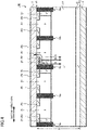
- Fig. 1 is a schematic cross-sectional view of the semiconductor device of the first embodiment.
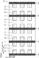
- Fig. 2 is a schematic top view of the semiconductor device of the first embodiment.
- Fig. 1 is a cross-sectional view taken along the line AA' of Fig. 2.
- Fig. 2 is a top view of a first face P1.
- the pin diode 100 of the first embodiment includes a semiconductor layer 10, an anode electrode 12 (first electrode), a cathode electrode 14 (second electrode), and a trench insulating layer 15.
- a trench 20a first trench
- a trench 20b second trench
- a trench 20c trench
- a trench 20d trench
- a trench 20e trench
- a cathode region 22 drift region
- a base region 26 second semiconductor region
- a channel region 28 third semiconductor region
- a first anode region 30a fourth semiconductor region
- a second anode region 30b fifth semiconductor region
- the anode electrode 12 is an example of the first electrode.
- the cathode electrode 14 is an example of the second electrode.
- the trench 20a is an example of the first trench.
- the trench 20b is an example of the second trench.
- the drift region 24 is an example of the first semiconductor region.
- the base region 26 is an example of the second semiconductor region.
- the channel region 28 is an example of the third semiconductor region.
- the first anode region 30a is an example of the fourth semiconductor region.
- the second anode region 30b is an example of the fifth semiconductor region.
- trench 20a the trench 20b, the trench 20c, the trench 20d, and the trench 20e may be collectively referred to as a trench 20.
- the semiconductor layer 10 has a first face P1 and a second face P2 opposite to the first face P1.
- the semiconductor layer 10 is, for example, single crystal silicon.
- the thickness of the semiconductor layer 10 is, for example, equal to or more than 40 ⁇ m and equal to or less than 700 ⁇ m.
- first direction one direction parallel to the first face P1 is referred to as a first direction.
- second direction a direction parallel to the first face P1 and perpendicular to the first direction.
- depth is defined as a distance in a direction toward the second face P2 with the first face P1 as a reference.
- the trench 20 is provided on the first face P1 side of the semiconductor layer 10.
- the trench 20 extends in a first direction on the first face P1.
- the trench 20 is repeatedly arranged in a second direction.
- a plurality of trenches 20 include the trench 20a, the trench 20b, the trench 20c, the trench 20d, and the trench 20e.
- the trench 20 is a groove provided in the semiconductor layer 10.
- the trench 20 is a part of the semiconductor layer 10.
- the trench 20 penetrates the base region 26 and reaches the drift region 24.
- the depth of the trench 20 is larger than the depth of the base region 26.
- the depth of the trench 20 is, for example, equal to or more than 2 ⁇ m and equal to or less than 10 ⁇ m.
- the width of the trench 20 in the second direction is, for example, equal to or more than 0.5 ⁇ m and equal to or less than 2 ⁇ m.
- the distance between the adjacent trenches 20 is larger than, for example, the depth of the trench 20.
- the distance between adjacent trenches 20a and 20b is larger than the depth of the trench 20a.
- the distance between the adjacent trenches 20 is, for example, equal to or more than 5 ⁇ m and equal to or less than 30 ⁇ m.
- the distance between the adjacent trenches 20 is larger than, for example, 10 ⁇ m.
- the trench insulating layer 15 is provided in the trench 20.
- the trench insulating layer 15 is, for example, silicon oxide.
- the cathode region 22 is an n + -type semiconductor region.
- the cathode region 22 is in contact with the second face P2.
- the drift region 24 is an n - -type semiconductor region.
- the drift region 24 is provided between the cathode region 22 and the first face P1.
- the drift region 24 is in contact with the bottom of the trench 20.
- the n-type impurity concentration in the drift region 24 is lower than the n-type impurity concentration in the cathode region 22.
- the n-type impurity concentration in the drift region 24 is, for example, equal to or more than 1 ⁇ 10 12 atoms/cm 3 and equal to or less than 1 ⁇ 10 15 atoms/cm 3 .
- the base region 26 is a p-type semiconductor region.
- the base region 26 is provided between the drift region 24 and the first face P1.
- the base region 26 is in contact with, for example, the drift region 24.
- the base region 26 extends in the first direction on the first face P1.
- the base region 26 is provided between two adjacent trenches 20.
- the base region 26 is provided, for example, between the trench 20a and the trench 20b.
- the base region 26 is provided, for example, between the trench 20a and the trench 20c.
- the base region 26 is in contact with the side surfaces of at least some of the trenches 20.
- the base region 26 is in contact with, for example, the side surface of the trench 20b.
- the base region 26 is in contact with, for example, the side surface of the trench 20c.
- the base region 26 is spaced from at least some of the trenches 20.
- the base region 26 is spaced from, for example, the trench 20a.
- the p-type impurity concentration in the base region 26 is, for example, equal to or more than 1 ⁇ 10 16 atoms/cm 3 and equal to or less than 5 ⁇ 10 17 atoms/cm 3 .
- the depth of the base region 26 is smaller than the depth of the trench 20.
- the depth of the base region 26 is larger than, for example, half the depth of the trench.
- the depth of the base region 26 is, for example, equal to or more than 2 ⁇ m and equal to or less than 8 ⁇ m.
- the channel region 28 is an n - -type semiconductor region.
- the channel region 28 is provided between the drift region 24 and the first face P1.
- the channel region 28 is provided between some of the trenches 20 and the base region 26.
- the channel region 28 is provided, for example, between the trench 20a and the base region 26.
- the channel region 28 is provided, for example, between the trench 20d and the base region 26.
- the channel region 28 is provided, for example, between the trench 20e and the base region 26.
- the channel region 28 is in contact with the side surfaces of some of the trenches 20.
- the channel region 28 is in contact with, for example, the side surface of the trench 20a.
- the channel region 28 is in contact with, for example, the side surface of the trench 20d.
- the channel region 28 is in contact with, for example, the side surface of the trench 20e.
- the channel region 28 is in contact with the base region 26.
- the n-type impurity concentration in the channel region 28 is higher than, for example, the n-type impurity concentration in the drift region 24.
- the n-type impurity concentration in the channel region 28 is, for example, equal to or more than 1 ⁇ 10 12 atoms/cm 3 and equal to or less than 1 ⁇ 10 16 atoms/cm 3 .
- the first anode region 30a is a p-type semiconductor region.
- the first anode region 30a is provided between the channel region 28 and the first face P1.
- the first anode region 30a extends in the first direction on the first face P1.
- the first anode region 30a is in contact with the side surfaces of some of the trenches 20.
- the first anode region 30a is in contact with, for example, the side surface of the trench 20a.
- the first anode region 30a is in contact with, for example, the side surface of the trench 20d.
- the first anode region 30a is in contact with, for example, the side surface of the trench 20e.
- the first anode region 30a is in contact with the base region 26.
- the p-type impurity concentration in the first anode region 30a is higher than the p-type impurity concentration in the base region 26.
- the p-type impurity concentration in the first anode region 30a is, for example, equal to or more than 1 ⁇ 10 17 atoms/cm 3 and equal to or less than 1 ⁇ 10 21 atoms/cm 3 .
- the depth of the first anode region 30a is smaller than the depth of the base region 26.
- the depth of the first anode region 30a is, for example, equal to or more than 0.1 ⁇ m and equal to or less than 2 ⁇ m.
- the width of the first anode region 30a in the second direction is larger than the width of the channel region 28 in the second direction.
- the second anode region 30b is a p-type semiconductor region.
- the second anode region 30b is provided between the base region 26 and the first face P1.
- the second anode region 30b extends in the first direction on the first face P1.
- the base region 26 is provided between the second anode region 30b and the first anode region 30a.
- the second anode region 30b is in contact with the base region 26.
- the second anode region 30b is in contact with the side surfaces of some of the trenches 20.
- the second anode region 30b is in contact with, for example, the side surface of the trench 20b.
- the second anode region 30b is in contact with, for example, the side surface of the trench 20c.
- the p-type impurity concentration in the second anode region 30b is higher than the p-type impurity concentration in the base region 26.
- the p-type impurity concentration in the second anode region 30b is, for example, equal to or more than 1 ⁇ 10 17 atoms/cm 3 and equal to or less than 1 ⁇ 10 21 atoms/cm 3 .
- the depth of the second anode region 30b is smaller than the depth of the base region 26.
- the depth of the second anode region 30b is, for example, equal to or more than 0.1 ⁇ m and equal to or less than 2 ⁇ m.
- the anode electrode 12 is provided on the first face P1 side of the semiconductor layer 10.
- the anode electrode 12 is in contact with the first face P1 of the semiconductor layer 10.
- the anode electrode 12 includes a first portion 12a and a second portion 12b.
- the anode electrode 12 is in contact with the base region 26, for example, at the first portion 12a.
- the anode electrode 12 is in contact with the first anode region 30a and the second anode region 30b, for example, at the second portion 12b.
- the anode electrode 12 makes Schottky contact with the base region 26, for example, at the first portion 12a.
- the anode electrode 12 makes ohmic contact with the first anode region 30a and the second anode region 30b, for example, at the second portion 12b.
- the anode electrode 12 is, for example, a metal.
- the material of the first portion 12a may be different from the material of the second portion 12b.
- the cathode electrode 14 is provided on the second face P2 side of the semiconductor layer 10.
- the cathode electrode 14 is in contact with the second face P2 of the semiconductor layer 10.
- the cathode electrode 14 is in contact with the cathode region 22.
- the cathode electrode 14 makes ohmic contact with the cathode region 22.
- the cathode electrode 14 is, for example, a metal.
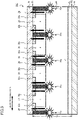
- Figs. 3 and 4 are explanatory diagrams of the function and effect of the semiconductor device of the first embodiment.
- Fig. 3 shows the flow of electrons (electron current) when the pin diode 100 is ON.
- Fig. 4 shows the flow of holes (hole current) when the pin diode 100 is ON.
- a forward bias is applied between the anode electrode 12 and the cathode electrode 14. That is, a voltage is applied between the anode electrode 12 and the cathode electrode 14 so that the electric potential of the anode electrode 12 is higher than the electric potential of the cathode electrode 14. That is, a voltage is applied between the anode electrode 12 and the cathode electrode 14 so that the side of the anode electrode 12 becomes positive.
- the anode electrode 12 serves as a positive electrode
- the cathode electrode 14 serves as a negative electrode.
- the cathode electrode 14 makes ohmic contact with the cathode region 22. Therefore, electrons ("e" in Fig. 3 ) injected from the cathode electrode 14 reach immediately below the p-type base region 26 from the n + -type cathode region 22 through the n - -type drift region 24.
- the pin diode 100 has an n - -type channel region 28 on the side surfaces of some of the trenches 20. Therefore, the electrons that have reached immediately below the base region 26 bypass the energy barrier between the drift region 24 and the base region 26 and flow to the channel region 28 having a low potential. The electrons flow immediately below the first anode region 30a of p + - type.
- the electrons that have reached immediately below the first anode region 30a bypass the energy barrier between the first anode region 30a and the channel region 28 and flow to the base region 26 having a low potential.
- the electrons flow immediately below the anode electrode 12.
- the base region 26 makes Schottky contact with the anode electrode 12. That is, the contact between the base region 26 and the anode electrode 12 is a Schottky contact between the p-type semiconductor and the metal. Therefore, the contact between the base region 26 and the anode electrode 12 serves as an energy barrier for holes but not for electrons. Therefore, electrons flow from the base region 26 to the anode electrode 12.
- the electrons that have reached immediately below the first anode region 30a bypass the energy barrier between the first anode region 30a and the channel region 28 and flow to the base region 26 having a low potential. As shown in Fig. 4 , the electrons move laterally below the first anode region 30a and flow to the base region 26.
- This lateral movement of the electrons causes a voltage drop below the first anode region 30a. Due to the voltage drop that occurs in the first anode region 30a, as shown in Fig. 4 , the first anode region 30a and the channel region 28 immediately below the first anode region 30a are in a forward bias state. In addition, the first anode region 30a and the base region 26 immediately below the first anode region 30a are in a forward bias state.
- the injected holes flow to the cathode electrode 14 through the drift region 24 and the cathode region 22.
- the hole current flows from the anode electrode 12 to the cathode electrode 14.
- the hole current increases as the width or depth of the first anode region 30a in the second direction increases.
- the hole current increases as the contact area between the first anode region 30a and the anode electrode 12 increases.
- the amount of holes injected from the anode electrode 12 can be adjusted by adjusting the width or depth of the first anode region 30a in the second direction or the contact area between the first anode region 30a and the anode electrode 12.
- Some of the electrons are injected from the drift region 24 into the base region 26 without passing through the channel region 28. This electron injection causes hole injection from the base region 26 into the drift region 24.
- a recovery loss occurs in a reverse recovery operation at which switching from the forward bias to the reverse bias occurs.
- a recovery current flows in the reverse direction because the carriers injected into the drift region are discharged. This current causes a recovery loss.
- the recovery loss can be reduced by reducing the carriers injected into the drift region.
- the carriers injected into the drift region 24 can be reduced by providing the channel region 28. Therefore, according to the pin diode 100 of the first embodiment, the recovery loss can be reduced.
- Fig. 5 is an explanatory diagram of the function and effect of the semiconductor device of the first embodiment.
- Fig. 5 is an explanatory diagram of the reverse recovery operation of the pin diode 100.
- the pin diode 100 switches from ON to OFF.
- the voltage applied between the anode electrode 12 and the cathode electrode 14 changes from the forward bias to the reverse bias.
- the pin diode 100 When the pin diode 100 is turned off, the voltage between the anode electrode 12 and the cathode electrode 14 is changed so that the electric potential of the anode electrode 12 is lower than the electric potential of the cathode electrode 14. That is, when the pin diode 100 is turned off, a voltage is applied between the anode electrode 12 and the cathode electrode 14 so that the side of the cathode electrode 14 becomes positive.
- the anode electrode 12 serves as a negative electrode
- the cathode electrode 14 serves as a positive electrode.
- the reverse recovery safe operating area is a current-voltage usable area in the reverse recovery operation.
- avalanche current Due to the avalanche breakdown that occurs at the bottom of the trench 20, a large amount of carriers are generated. The flow of the generated carriers is referred to as an avalanche current. If the avalanche current increases, the pin diode may be damaged. For example, when the avalanche current is concentrated at a specific location, the temperature rises and the pin diode is damaged.
- the first anode region 30a of p + -type or the second anode region 30b of p + -type are provided on both sides of the trench 20.
- the holes generated by the avalanche breakdown at the bottom of the trench 20 are discharged to the anode electrode 12 at the shortest distance from the bottom of the trench 20 through the first anode region 30a or the second anode region 30b.
- the trenches 20 are provided in the semiconductor layer 10 at a predetermined ratio. For this reason, at the time of turn-off, the avalanche breakdown occurs at dispersed places.
- the first anode region 30a of p + - type or the second anode region 30b of p + -type serving as a hole discharge path is provided on both sides of each trench 20, the first anode region 30a of p + - type or the second anode region 30b of p + -type serving as a hole discharge path is provided. For this reason, the hole discharge path is also dispersed.
- the avalanche current is unlikely to be concentrated at a specific location. Therefore, according to the pin diode 100, the damage in the reverse recovery operation is suppressed, so that the reverse recovery safe operating area can be expanded.
- the first anode region 30a or the second anode region 30b is provided on both sides of the trench 20 regardless of the presence or absence of the channel region 28 in contact with the trench 20. Therefore, from the viewpoint of reducing the recovery loss, even if the occupancy ratio of the channel region 28 in the semiconductor layer 10 is reduced, the damage in the reverse recovery operation can be suppressed.
- the distance between the adjacent trenches 20 is large.
- the distance between the adjacent trenches 20 is larger than, for example, the depth of the trench 20.
- the distance between the adjacent trenches 20 is preferably equal to or more than 1.5 times the depth of the trench 20, more preferably equal to or more than 2 times the depth of the trench 20.
- the distance between the adjacent trenches 20 is preferably larger than 10 ⁇ m, more preferably equal to or more than 12 ⁇ m, and even more preferably equal to or more than 15 ⁇ m.
- the breakdown voltage of the pin diode 100 may decrease.
- the depth of the base region 26 is preferably equal to or more than half the depth of the trench 20, more preferably equal to or more than three-quarters of the depth of the trench 20, and even more preferably equal to or more than nine-tenths of the depth of the trench 20.
- the n-type impurity concentration in the channel region 28 is higher than the n-type impurity concentration in the drift region 24.
- the material of the first portion 12a of the anode electrode 12 is different from the material of the second portion 12b. It can be easily realized to make the contact between the first portion 12a and the base region 26 as Schottky contact and the contact between the second portion 12b and each of the first anode region 30a and the second anode region 30b as ohmic contact.
- Fig. 6 is a schematic top view of a modification example of the semiconductor device of the first embodiment.
- the modification example of the semiconductor device of the first embodiment is a pin diode 101.
- the pin diode 101 is different from the pin diode 101 of the first embodiment in that the first anode region 30a and the second anode region 30b are arranged so as to be divided into a plurality of parts in the first direction.
- the channel region 28 below the first anode region 30a is also arranged so as to be divided into a plurality of parts in the first direction.
- a semiconductor device of a second embodiment is different from the semiconductor device of the first embodiment in that the fifth semiconductor region in contact with the first trench is provided with the first trench interposed between the fourth semiconductor region and the fifth semiconductor region.
- the description of the content overlapping the first embodiment will be omitted.
- the semiconductor device of the second embodiment is a pin diode 200.
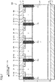
- Fig. 7 is a schematic cross-sectional view of the semiconductor device of the second embodiment.
- the pin diode 200 of the second embodiment includes a semiconductor layer 10, an anode electrode 12 (first electrode), a cathode electrode 14 (second electrode), and a trench insulating layer 15.
- a trench 20a first trench
- a trench 20b second trench
- a trench 20c trench
- a trench 20d trench
- a trench 20e trench
- a cathode region 22 drift region
- a base region 26 second semiconductor region
- a channel region 28 third semiconductor region
- a first anode region 30a fourth semiconductor region
- a second anode region 30b fifth semiconductor region
- the anode electrode 12 is an example of the first electrode.
- the cathode electrode 14 is an example of the second electrode.
- the trench 20a is an example of the first trench.
- the trench 20b is an example of the second trench.
- the drift region 24 is an example of the first semiconductor region.
- the base region 26 is an example of the second semiconductor region.
- the channel region 28 is an example of the third semiconductor region.
- the first anode region 30a is an example of the fourth semiconductor region.
- the second anode region 30b is an example of the fifth semiconductor region.
- trench 20a the trench 20b, the trench 20c, the trench 20d, and the trench 20e may be collectively referred to as a trench 20.
- the first anode region 30a and the second anode region 30b are provided with the trench 20 interposed therebetween.
- the trench 20 is provided between the first anode region 30a and the second anode region 30b.
- the first anode region 30a is in contact with one side surface of the same trench 20, and the second anode region 30b is in contact with the other side surface.
- first anode region 30a and the second anode region 30b are provided with the trench 20a interposed therebetween.
- the trench 20a is provided between the first anode region 30a and the second anode region 30b.
- the first anode region 30a is in contact with one side surface of the trench 20a, and the second anode region 30b is in contact with the other side surface.
- the bias of the distribution of the channel region 28 in the semiconductor layer 10 is smaller than that in the pin diode 100 of the first embodiment. Therefore, the hole injection into the drift region 24 becomes more uniform. As a result, the current flow of the pin diode 200 becomes more uniform.
- a semiconductor device of a third embodiment is different from the semiconductor device of the first embodiment in that a third electrode provided in the first trench and the second trench and electrically separated from the first electrode and the second electrode is further provided.
- a third electrode provided in the first trench and the second trench and electrically separated from the first electrode and the second electrode is further provided.
- a semiconductor circuit of the third embodiment includes: the semiconductor device described above; and a control circuit for driving the semiconductor device and for applying a voltage negative with respect to the first electrode to the third electrode with a voltage making a side of the second electrode positive being applied between the first electrode and the second electrode when the first conductive type is an n type and applying a voltage positive with respect to the first electrode to the third electrode with a voltage making the side of the second electrode negative being applied between the first electrode and the second electrode when the first conductive type is a p type.
- the semiconductor device of the third embodiment is a pin diode 300.
- a control circuit of the third embodiment is a gate driver circuit 350.
- a semiconductor circuit of the third embodiment includes a semiconductor device and a control circuit for controlling the semiconductor device.
- the first conductive type is the n type and the second conductive type is the p type will be described as an example.
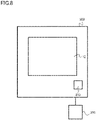
- Fig. 8 is a schematic diagram of the semiconductor circuit of the third embodiment.
- the semiconductor circuit of the third embodiment includes the pin diode 300 and the gate driver circuit 350.
- the gate driver circuit 350 controls the pin diode 300.
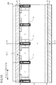
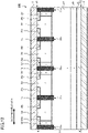
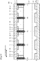
- Fig. 9 is a schematic cross-sectional view of the semiconductor device of the third embodiment.
- the pin diode 300 of the third embodiment includes a semiconductor layer 10, an anode electrode 12 (first electrode), a cathode electrode 14 (second electrode), a trench gate insulating film 16, a trench gate electrode 18 (third electrode), an interlayer insulating layer 19, and an electrode pad 310.
- a trench 20a first trench
- a trench 20b second trench
- a trench 20c trench
- a trench 20d trench
- a trench 20e trench
- a cathode region 22 drift region
- a base region 26 second semiconductor region
- a channel region 28 third semiconductor region
- a first anode region 30a fourth semiconductor region
- a second anode region 30b fifth semiconductor region
- the anode electrode 12 is an example of the first electrode.
- the cathode electrode 14 is an example of the second electrode.
- the trench gate electrode 18 is an example of the third electrode.
- the trench 20a is an example of the first trench.
- the trench 20b is an example of the second trench.
- the drift region 24 is an example of the first semiconductor region.
- the base region 26 is an example of the second semiconductor region.
- the channel region 28 is an example of the third semiconductor region.
- the first anode region 30a is an example of the fourth semiconductor region.
- the second anode region 30b is an example of the fifth semiconductor region.
- trench 20a the trench 20b, the trench 20c, the trench 20d, and the trench 20e may be collectively referred to as a trench 20.
- the trench gate electrode 18 is provided in the trench 20.
- the trench gate electrode 18 is provided, for example, in the trench 20a.
- the trench gate electrode 18 is provided, for example, in the trench 20b.
- the trench gate electrode 18 is provided, for example, in the trench 20c.
- the trench gate electrode 18 is, for example, a semiconductor or a metal.
- the trench gate electrode 18 is, for example, amorphous silicon or polycrystalline silicon containing n-type impurities or p-type impurities.
- the trench gate electrode 18 is electrically separated from the anode electrode 12 and the cathode electrode 14.
- the trench gate electrode 18 is electrically connected to the electrode pad 310.
- the trench gate insulating film 16 is provided between the trench gate electrode 18 and the semiconductor layer 10.
- the trench gate insulating film 16 is, for example, silicon oxide.
- the interlayer insulating layer 19 is provided between the trench gate electrode 18 and the anode electrode 12.
- the interlayer insulating layer 19 electrically separates the trench gate electrode 18 from the anode electrode 12.
- the interlayer insulating layer 19 is, for example, silicon oxide.
- the electrode pad 310 is provided on the first face P1 side of the semiconductor layer 10.
- the electrode pad 310 is electrically connected to the trench gate electrode 18.
- the electrode pad 310 and the trench gate electrode 18 are connected to each other by, for example, a metal wiring (not shown).
- Figs. 10 , 11 , and 12 are explanatory diagrams of the function and effect of the semiconductor device and the semiconductor circuit of the third embodiment.
- Fig. 10 is a schematic diagram showing a voltage applied to the pin diode.
- Fig. 11 is an example of the timing chart of the voltage applied to the pin diode.
- Fig. 12 is an explanatory diagram of the reverse recovery operation of the pin diode 300.
- a first voltage (V1) is applied to the anode electrode 12 of the pin diode 300
- a second voltage (V2) is applied to the cathode electrode 14
- a third voltage (V3) is applied to the trench gate electrode 18.
- the third voltage (V3) applied to the trench gate electrode 18 is controlled by, for example, the gate driver circuit 350.
- a voltage is applied between the anode electrode 12 and the cathode electrode 14 so that the electric potential of the anode electrode 12 is higher than the electric potential of the cathode electrode 14.
- a voltage is applied between the anode electrode 12 and the cathode electrode 14 so that the side of the anode electrode 12 becomes positive. That is, in the ON state, a first voltage V1 applied to the anode electrode 12 is higher than a second voltage V2 applied to the cathode electrode 14.
- a third voltage V3 applied to the trench gate electrode 18 is, for example, 0 V, which is equal to the first voltage V1.
- the voltage between the anode electrode 12 and the cathode electrode 14 is changed so that the electric potential of the anode electrode 12 is lower than the electric potential of the cathode electrode 14. That is, at the time of turn-off, a voltage is applied between the anode electrode 12 and the cathode electrode 14 so that the side of the cathode electrode 14 becomes positive. That is, at the time of turn-off, the second voltage V2 applied to the cathode electrode 14 becomes higher than the first voltage V1 applied to the anode electrode 12.
- the first voltage V1 is 0 V and the second voltage V2 is a positive voltage.
- the third voltage V3 applied to the trench gate electrode 18 is a negative voltage.
- a voltage that is negative with respect to the anode electrode 12 is applied to the trench gate electrode 18.
- a p-type accumulation layer is formed in the semiconductor layer 10 on the side surface of the trench 20.
- the formation of the p-type accumulation layer in the semiconductor layer 10 on the side surface of the trench 20 promotes the discharge of holes from the drift region 24 at the time of turn-off. Therefore, the recovery loss of the pin diode 300 is further reduced as compared with the pin diode 100 of the first embodiment.
- the formation of the p-type accumulation layer in the semiconductor layer 10 on the side surface of the trench 20 also promotes the discharge of holes generated by the avalanche breakdown at the bottom of the trench 20. Therefore, according to the pin diode 300, as compared with the pin diode 100, the damage in the reverse recovery operation is further suppressed, so that the reverse recovery safe operating area can be further expanded.
- timing chart shown in Fig. 11 is an example of the operation of the pin diode 300.
- an operation of applying a voltage equal to the anode electrode 12 or a positive voltage to the trench gate electrode 18 when the pin diode 300 is turned off is not excluded.
- the third embodiment it is possible to provide a pin diode having a reduced recovery loss and an expanded safe operating area and a semiconductor circuit including the pin diode.
- a semiconductor device of a fourth embodiment is different from the semiconductor device of the first embodiment in that the semiconductor layer further includes a semiconductor region of a first conductive type between the first semiconductor region and the second face.
- the description of a part of the content overlapping the first embodiment may be omitted.
- the semiconductor device of the fourth embodiment is a pin diode 400.
- Fig. 13 is a schematic cross-sectional view of the semiconductor device of the fourth embodiment.
- the pin diode 400 of the fourth embodiment includes a semiconductor layer 10, an anode electrode 12 (first electrode), a cathode electrode 14 (second electrode), and a trench insulating layer 15.
- a trench 20a first trench
- a trench 20b second trench
- a trench 20c trench
- a trench 20d trench
- a trench 20e trench
- a cathode region 22 drift region 24
- a base region 26 second semiconductor region
- a channel region 28 third semiconductor region
- a first anode region 30a fourth semiconductor region
- a second anode region 30b fifth semiconductor region
- a buffer region 32 is provided.
- the anode electrode 12 is an example of the first electrode.
- the cathode electrode 14 is an example of the second electrode.
- the trench 20a is an example of the first trench.
- the trench 20b is an example of the second trench.
- the drift region 24 is an example of the first semiconductor region.
- the base region 26 is an example of the second semiconductor region.
- the channel region 28 is an example of the third semiconductor region.
- the first anode region 30a is an example of the fourth semiconductor region.
- the second anode region 30b is an example of the fifth semiconductor region.
- the buffer region 32 is an n-type semiconductor region.
- the buffer region 32 is provided between the cathode region 22 and the drift region 24.
- the n-type impurity concentration in the buffer region 32 is lower than the n-type impurity concentration in the cathode region 22.
- the n-type impurity concentration in the buffer region 32 is higher than the n-type impurity concentration in the drift region 24.
- the buffer region 32 suppresses current oscillation and voltage oscillation during the reverse recovery operation.
- Fig. 14 is a schematic cross-sectional view of a first modification example of the semiconductor device of the fourth embodiment.
- the first modification example of the semiconductor device of the fourth embodiment is a pin diode 401.
- the pin diode 401 is different from the pin diode 400 of the fourth embodiment in that the cathode region 22 is divided into a plurality of parts in the second direction.
- the cathode electrode 14 makes ohmic contact with the cathode region 22.
- the cathode electrode 14 makes Schottky contact with the buffer region 32.
- the injection of electrons from the cathode electrode 14 is suppressed by dividing the cathode region 22 into a plurality of parts. Recovery loss is reduced by suppressing the injection of electrons.
- Fig. 15 is a schematic cross-sectional view of a second modification example of the semiconductor device of the fourth embodiment.
- the second modification example of the semiconductor device of the fourth embodiment is a pin diode 402.
- the pin diode 402 is different from the pin diode 401 of the first modification example of the fourth embodiment in that a p + -type region 34 is provided between the divided cathode regions 22.
- holes are injected from the cathode electrode 14 into the drift region 24 through the p + -type region 34 during the reverse recovery operation. Since the holes are injected into the drift region 24, current oscillation and voltage oscillation during the reverse recovery operation are suppressed.
- a semiconductor device of a fifth embodiment is different from the semiconductor device of the first embodiment in that the semiconductor device of the fifth embodiment is an RC-IGBT including the pin diode of the first embodiment.
- the description of a part of the content overlapping the first embodiment will be omitted.
- the semiconductor device of the fifth embodiment is an RC-IGBT 500 in which an IGBT and a freewheeling diode are formed in the same semiconductor chip.
- the RC-IGBT 500 has a trench gate type IGBT including a gate electrode in a trench formed in a semiconductor layer.
- the RC-IGBT 500 includes the pin diode 100 of the first embodiment as a freewheeling diode.
- the first conductive type is the n type and the second conductive type is the p type will be described as an example.
- Fig. 16 is a schematic cross-sectional view of the semiconductor device of the fifth embodiment.
- the RC-IGBT 500 of the fifth embodiment has an IGBT region 501 and a diode region 502.
- the diode region 502 includes the pin diode 100 of the first embodiment.
- the IGBT region 501 operates as an IGBT.
- the diode region 502 operates as a freewheeling diode.
- the RC-IGBT 500 of the fifth embodiment includes a semiconductor layer 10, an upper electrode 62 (first electrode), a lower electrode 64 (second electrode), a gate insulating film 41, a gate electrode 51, an interlayer insulating layer 61, and a trench insulating layer 15.
- a gate trench 71 In the semiconductor layer 10 of the IGBT region 501, a gate trench 71, a p + -type collector region 78, an n - -type drift region 24, a p-type body region 74, an n-type emitter region 76, and a p-type contact region 80 are provided.
- a trench 20a first trench
- a trench 20b second trench
- a trench 20c a cathode region 22
- drift region 24 first semiconductor region
- base region 26 second semiconductor region
- channel region 28 third semiconductor region
- first anode region 30a fourth semiconductor region
- second anode region 30b second anode region
- the upper electrode 62 functions as an emitter electrode of the IGBT.
- the upper electrode 62 functions as an anode electrode of the diode.
- the lower electrode 64 functions as a collector electrode of the IGBT.
- the lower electrode 64 functions as a cathode electrode of the diode.
- the gate electrode 51 functions as a gate electrode of the transistor of the IGBT.
- a gate voltage (Vg) is applied to the gate electrode 51.
- the RC-IGBT 500 includes a pin diode, which has a reduced recovery loss and an expanded safe operating area, in the same semiconductor chip. Therefore, it is possible to realize the RC-IGBT 500 having a reduced recovery loss and an expanded safe operating area.
- the semiconductor layer is single crystal silicon
- the semiconductor layer is not limited to the single crystal silicon.
- other single crystal semiconductors such as single crystal silicon carbide, may be used.
- the first conductive type is the n type and the second conductive type is the p type has been described as an example.
- the first conductive type can be the p type and the second conductive type can be the n type.
- the first conductive type is the p type and the second conductive type is the n type, for example, in the pin diode 300 of the third embodiment, at the time of turn-off, as the third voltage V3 applied to the trench gate electrode 18, a voltage that is positive with respect to the first voltage V1 applied to the anode electrode 12 is applied.
- the configuration in which the RC-IGBT includes the pin diode of the first embodiment has been described as an example. However, it is also possible to adopt a configuration in which the RC-IGBT includes the pin diode of each of the second to fourth embodiments.
Landscapes
- Electrodes Of Semiconductors (AREA)
- Metal-Oxide And Bipolar Metal-Oxide Semiconductor Integrated Circuits (AREA)
Abstract
A semiconductor device of embodiments includes: a semiconductor layer including a first trench, a second trench, a first semiconductor region of a first conductive type, a second semiconductor region of a second conductive type provided between a first face and the first semiconductor region, between the first trench and the second trench, and in contact with the second trench, a third semiconductor region of a first conductive type provided between the first trench and the second semiconductor region, a fourth semiconductor region of a second conductive type provided between the third semiconductor region and the first face, and a fifth semiconductor region of a second conductive type provided between the second semiconductor region and the first face, spaced from the fourth semiconductor region, in contact with the second trench; a first electrode on a first face side; and a second electrode on a second face side.
Description
- This application is based upon and claims the benefit of priority from
Japanese Patent Application No. 2021-040092, filed on March 12, 2021 - Embodiments described herein relate generally to a semiconductor device and a semiconductor circuit.
- An example of a power semiconductor device is an insulated gate bipolar transistor (IGBT). In the IGBT, for example, a p-type collector region, an n-type drift region, and a p-type base region are provided on a collector electrode. Then, in a trench that penetrates the p-type base region and reaches the n-type drift region, a gate electrode is provided with a gate insulating film interposed therebetween. In addition, an n-type emitter region connected to an emitter electrode is provided in a region adjacent to the trench on the surface of the p-type base region.
- In recent years, a reverse-conducting IGBT (RC-IGBT) in which an IGBT and a freewheeling diode are formed in the same semiconductor chip has been widely developed and commercialized. The RC-IGBT is used, for example, as a switching element in an inverter circuit. The freewheeling diode has a function of making a current flow in a direction opposite to the on-current of the IGBT. The freewheeling diode is formed, for example, by a pin (p-intrinsic-n) diode having a pn junction.
- In the pin diode, a recovery loss occurs in a reverse recovery operation at which switching from the forward bias to the reverse bias occurs. In other words, the reverse recovery operation is a switching operation when the pin diode is turned off. In the reverse recovery operation, a recovery current flows in the reverse direction to discharge the carriers injected into the drift region. This current causes a recovery loss. In order to reduce the recovery loss, various structures for reducing the carriers injected into the drift region have been proposed.
- In addition, in the reverse recovery operation of the pin diode, electric field concentration may occur at a specific location of the pn junction to cause avalanche breakdown. Then, when the avalanche breakdown occurs and the flowing current increases, the pin diode may be damaged. By suppressing the damage to the pin diode in the reverse recovery operation, the reverse recovery safe operating area can be expanded. The reverse recovery safe operating area is a current-voltage usable area in the reverse recovery operation.
-
-
Fig. 1 is a schematic cross-sectional view of a semiconductor device of a first embodiment; -
Fig. 2 is a schematic top view of the semiconductor device of the first embodiment; -
Fig. 3 is an explanatory diagram of the function and effect of the semiconductor device of the first embodiment; -
Fig. 4 is an explanatory diagram of the function and effect of the semiconductor device of the first embodiment; -
Fig. 5 is an explanatory diagram of the function and effect of the semiconductor device of the first embodiment; -
Fig. 6 is a schematic top view of a modification example of the semiconductor device of the first embodiment; -
Fig. 7 is a schematic cross-sectional view of a semiconductor device of a second embodiment; -
Fig. 8 is a schematic diagram of a semiconductor circuit of a third embodiment; -
Fig. 9 is a schematic cross-sectional view of a semiconductor device of the third embodiment; -
Fig. 10 is an explanatory diagram of the function and effect of the semiconductor device and the semiconductor circuit of the third embodiment; -
Fig. 11 is an explanatory diagram of the function and effect of the semiconductor device and the semiconductor circuit of the third embodiment; -
Fig. 12 is an explanatory diagram of the function and effect of the semiconductor device and the semiconductor circuit of the third embodiment; -
Fig. 13 is a schematic cross-sectional view of a semiconductor device of a fourth embodiment; -
Fig. 14 is a schematic cross-sectional view of a first modification example of the semiconductor device of the fourth embodiment; -
Fig. 15 is a schematic cross-sectional view of a second modification example of the semiconductor device of the fourth embodiment; and -
Fig. 16 is a schematic cross-sectional view of a semiconductor device of a fifth embodiment. - A semiconductor device of embodiments includes: a semiconductor layer having a first face and a second face opposite to the first face and including: a first trench provided in a first face side; a second trench provided in a first face side; a first semiconductor region of a first conductive type in contact with the first trench and the second trench; a second semiconductor region of a second conductive type provided between the first face and the first semiconductor region, the second semiconductor region provided between the first trench and the second trench, and the second semiconductor region being in contact with the second trench; a third semiconductor region of a first conductive type provided between the first semiconductor region and the first face, the third semiconductor region provided between the first trench and the second semiconductor region, the third semiconductor region being in contact with the first trench, and the third semiconductor region being in contact with the second semiconductor region; a fourth semiconductor region of a second conductive type provided between the third semiconductor region and the first face, the fourth semiconductor region provided between the first trench and the second semiconductor region, the fourth semiconductor region being in contact with the first trench, the fourth semiconductor region being in contact with the second semiconductor region, and the fourth semiconductor region being having a second conductive type impurity concentration higher than a second conductive type impurity concentration in the second semiconductor region; and a fifth semiconductor region of a second conductive type provided between the second semiconductor region and the first face, the fifth semiconductor region being in contact with the second trench, and the fifth semiconductor region being having a second conductive type impurity concentration higher than the second conductive type impurity concentration in the second semiconductor region, and the second semiconductor region being provided between the fourth semiconductor region and the fifth semiconductor region; a first electrode provided on the first face side of the semiconductor layer and in contact with the second semiconductor region, the fourth semiconductor region, and the fifth semiconductor region; and a second electrode provided on a second face side of the semiconductor layer.
- Hereinafter, embodiments will be described with reference to the diagrams. In the following description, the same or similar members and the like are denoted by the same reference numerals, and the description of the members and the like once described will be omitted as appropriate.
- In this specification, when there is a notation of n+ type, n type, and n- type, this means that the impurity concentration of n type decreases in the order of n+ type, n type, and n- type. In addition, when there is a notation of p+ type, p type, and p- type, this means that the impurity concentration of p type decreases in the order of p+ type, p type, and p- type.
- In this specification, the distribution and absolute value of the impurity concentration in a semiconductor region can be measured by using, for example, secondary ion mass spectrometry (SIMS). In addition, the relative magnitude relationship between the impurity concentrations in two semiconductor regions can be determined by using, for example, scanning capacitance microscopy (SCM). In addition, the distribution and absolute value of the impurity concentration can be measured by using, for example, spreading resistance analysis (SRA). By the SCM and the SRA, the relative magnitude relationship or absolute values of the carrier concentrations in semiconductor regions can be calculated. By assuming the activation rate of impurities, the relative magnitude relationship between the impurity concentrations in two semiconductor regions, the distribution of the impurity concentration, and the absolute value of the impurity concentration can be calculated from the measurement results of the SCM and the SRA.
- In addition, in this specification, the "p-type impurity concentration" in the p-type semiconductor region means the net p-type impurity concentration obtained by subtracting the n-type impurity concentration in the region from the p-type impurity concentration in the region. In addition, the "n-type impurity concentration" in the n-type semiconductor region means the net n-type impurity concentration obtained by subtracting the p-type impurity concentration in the region from the n-type impurity concentration in the region.
- In addition, unless otherwise specified in this specification, the impurity concentration in a specific region means the maximum value of the impurity concentration in the region.
- A semiconductor device of a first embodiment includes: a semiconductor layer having a first face and a second face opposite to the first face and including: a first trench provided in a first face side; a second trench provided in a first face side; a first semiconductor region of a first conductive type in contact with the first trench and the second trench; a second semiconductor region of a second conductive type provided between the first face and the first semiconductor region, the second semiconductor region provided between the first trench and the second trench, and the second semiconductor region being in contact with the second trench; a third semiconductor region of a first conductive type provided between the first semiconductor region and the first face, the third semiconductor region provided between the first trench and the second semiconductor region, the third semiconductor region being in contact with the first trench, and the third semiconductor region being in contact with the second semiconductor region; a fourth semiconductor region of a second conductive type provided between the third semiconductor region and the first face, the fourth semiconductor region provided between the first trench and the second semiconductor region, the fourth semiconductor region being in contact with the first trench, the fourth semiconductor region being in contact with the second semiconductor region, and the fourth semiconductor region being having a second conductive type impurity concentration higher than a second conductive type impurity concentration in the second semiconductor region; and a fifth semiconductor region of a second conductive type provided between the second semiconductor region and the first face, the fifth semiconductor region being in contact with the second trench, and the fifth semiconductor region being having a second conductive type impurity concentration higher than the second conductive type impurity concentration in the second semiconductor region, and the second semiconductor region being provided between the fourth semiconductor region and the fifth semiconductor region; a first electrode provided on the first face side of the semiconductor layer and in contact with the second semiconductor region, the fourth semiconductor region, and the fifth semiconductor region; and a second electrode provided on a second face side of the semiconductor layer.
- The semiconductor device of the first embodiment is a
pin diode 100. Thepin diode 100 is, for example, a fast recovery diode (FRD). Thepin diode 100 is used, for example, as a freewheeling diode in an inverter circuit or the like. In addition, thepin diode 100 is used, for example, as a diode for the RC-IGBT. - Hereinafter, a case where the first conductive type is the n type and the second conductive type is the p type will be described as an example.
-
Fig. 1 is a schematic cross-sectional view of the semiconductor device of the first embodiment.Fig. 2 is a schematic top view of the semiconductor device of the first embodiment.Fig. 1 is a cross-sectional view taken along the line AA' ofFig. 2. Fig. 2 is a top view of a first face P1. - The
pin diode 100 of the first embodiment includes asemiconductor layer 10, an anode electrode 12 (first electrode), a cathode electrode 14 (second electrode), and atrench insulating layer 15. - In the
semiconductor layer 10, atrench 20a (first trench), atrench 20b (second trench), atrench 20c, atrench 20d, atrench 20e, acathode region 22, a drift region 24 (first semiconductor region), a base region 26 (second semiconductor region), a channel region 28 (third semiconductor region), afirst anode region 30a (fourth semiconductor region), and asecond anode region 30b (fifth semiconductor region) are provided. - The anode electrode 12 is an example of the first electrode. The cathode electrode 14 is an example of the second electrode. The
trench 20a is an example of the first trench. Thetrench 20b is an example of the second trench. Thedrift region 24 is an example of the first semiconductor region. Thebase region 26 is an example of the second semiconductor region. Thechannel region 28 is an example of the third semiconductor region. Thefirst anode region 30a is an example of the fourth semiconductor region. Thesecond anode region 30b is an example of the fifth semiconductor region. - Hereinafter, the
trench 20a, thetrench 20b, thetrench 20c, thetrench 20d, and thetrench 20e may be collectively referred to as a trench 20. - The
semiconductor layer 10 has a first face P1 and a second face P2 opposite to the first face P1. Thesemiconductor layer 10 is, for example, single crystal silicon. The thickness of thesemiconductor layer 10 is, for example, equal to or more than 40 µm and equal to or less than 700 µm. - In this specification, one direction parallel to the first face P1 is referred to as a first direction. In addition, a direction parallel to the first face P1 and perpendicular to the first direction is referred to as a second direction. In addition, in this specification, the "depth" is defined as a distance in a direction toward the second face P2 with the first face P1 as a reference.
- The trench 20 is provided on the first face P1 side of the
semiconductor layer 10. The trench 20 extends in a first direction on the first face P1. The trench 20 is repeatedly arranged in a second direction. - A plurality of trenches 20 include the
trench 20a, thetrench 20b, thetrench 20c, thetrench 20d, and thetrench 20e. - The trench 20 is a groove provided in the
semiconductor layer 10. The trench 20 is a part of thesemiconductor layer 10. The trench 20 penetrates thebase region 26 and reaches thedrift region 24. - The depth of the trench 20 is larger than the depth of the
base region 26. The depth of the trench 20 is, for example, equal to or more than 2 µm and equal to or less than 10 µm. - The width of the trench 20 in the second direction is, for example, equal to or more than 0.5 µm and equal to or less than 2 µm.
- The distance between the adjacent trenches 20 is larger than, for example, the depth of the trench 20. For example, the distance between
adjacent trenches trench 20a. - The distance between the adjacent trenches 20 is, for example, equal to or more than 5 µm and equal to or less than 30 µm. The distance between the adjacent trenches 20 is larger than, for example, 10 µm.
- The
trench insulating layer 15 is provided in the trench 20. Thetrench insulating layer 15 is, for example, silicon oxide. - The
cathode region 22 is an n+-type semiconductor region. Thecathode region 22 is in contact with the second face P2. - The
drift region 24 is an n--type semiconductor region. Thedrift region 24 is provided between thecathode region 22 and the first face P1. Thedrift region 24 is in contact with the bottom of the trench 20. - The n-type impurity concentration in the
drift region 24 is lower than the n-type impurity concentration in thecathode region 22. The n-type impurity concentration in thedrift region 24 is, for example, equal to or more than 1 × 10¹² atoms/cm3 and equal to or less than 1 × 10¹⁵ atoms/cm3. - The
base region 26 is a p-type semiconductor region. Thebase region 26 is provided between thedrift region 24 and the first face P1. Thebase region 26 is in contact with, for example, thedrift region 24. Thebase region 26 extends in the first direction on the first face P1. - The
base region 26 is provided between two adjacent trenches 20. Thebase region 26 is provided, for example, between thetrench 20a and thetrench 20b. Thebase region 26 is provided, for example, between thetrench 20a and thetrench 20c. - The
base region 26 is in contact with the side surfaces of at least some of the trenches 20. Thebase region 26 is in contact with, for example, the side surface of thetrench 20b. Thebase region 26 is in contact with, for example, the side surface of thetrench 20c. - The
base region 26 is spaced from at least some of the trenches 20. Thebase region 26 is spaced from, for example, thetrench 20a. - The p-type impurity concentration in the
base region 26 is, for example, equal to or more than 1 × 10¹⁶ atoms/cm3 and equal to or less than 5 × 10¹⁷ atoms/cm3. - The depth of the
base region 26 is smaller than the depth of the trench 20. The depth of thebase region 26 is larger than, for example, half the depth of the trench. The depth of thebase region 26 is, for example, equal to or more than 2 µm and equal to or less than 8 µm. - The
channel region 28 is an n--type semiconductor region. Thechannel region 28 is provided between thedrift region 24 and the first face P1. - The
channel region 28 is provided between some of the trenches 20 and thebase region 26. Thechannel region 28 is provided, for example, between thetrench 20a and thebase region 26. Thechannel region 28 is provided, for example, between thetrench 20d and thebase region 26. Thechannel region 28 is provided, for example, between thetrench 20e and thebase region 26. - The
channel region 28 is in contact with the side surfaces of some of the trenches 20. Thechannel region 28 is in contact with, for example, the side surface of thetrench 20a. Thechannel region 28 is in contact with, for example, the side surface of thetrench 20d. Thechannel region 28 is in contact with, for example, the side surface of thetrench 20e. - The
channel region 28 is in contact with thebase region 26. - The n-type impurity concentration in the
channel region 28 is higher than, for example, the n-type impurity concentration in thedrift region 24. The n-type impurity concentration in thechannel region 28 is, for example, equal to or more than 1 × 10¹² atoms/cm3 and equal to or less than 1 × 10¹⁶ atoms/cm3. - The
first anode region 30a is a p-type semiconductor region. Thefirst anode region 30a is provided between thechannel region 28 and the first face P1. Thefirst anode region 30a extends in the first direction on the first face P1. - The
first anode region 30a is in contact with the side surfaces of some of the trenches 20. Thefirst anode region 30a is in contact with, for example, the side surface of thetrench 20a. Thefirst anode region 30a is in contact with, for example, the side surface of thetrench 20d. Thefirst anode region 30a is in contact with, for example, the side surface of thetrench 20e. - The
first anode region 30a is in contact with thebase region 26. - The p-type impurity concentration in the
first anode region 30a is higher than the p-type impurity concentration in thebase region 26. The p-type impurity concentration in thefirst anode region 30a is, for example, equal to or more than 1 × 10¹⁷ atoms/cm3 and equal to or less than 1 × 10²¹ atoms/cm3. - The depth of the
first anode region 30a is smaller than the depth of thebase region 26. The depth of thefirst anode region 30a is, for example, equal to or more than 0.1 µm and equal to or less than 2 µm. - The width of the
first anode region 30a in the second direction is larger than the width of thechannel region 28 in the second direction. - The
second anode region 30b is a p-type semiconductor region. Thesecond anode region 30b is provided between thebase region 26 and the first face P1. Thesecond anode region 30b extends in the first direction on the first face P1. - The
base region 26 is provided between thesecond anode region 30b and thefirst anode region 30a. Thesecond anode region 30b is in contact with thebase region 26. - The
second anode region 30b is in contact with the side surfaces of some of the trenches 20. Thesecond anode region 30b is in contact with, for example, the side surface of thetrench 20b. Thesecond anode region 30b is in contact with, for example, the side surface of thetrench 20c. - The p-type impurity concentration in the
second anode region 30b is higher than the p-type impurity concentration in thebase region 26. The p-type impurity concentration in thesecond anode region 30b is, for example, equal to or more than 1 × 10¹⁷ atoms/cm3 and equal to or less than 1 × 10²¹ atoms/cm3. - The depth of the
second anode region 30b is smaller than the depth of thebase region 26. The depth of thesecond anode region 30b is, for example, equal to or more than 0.1 µm and equal to or less than 2 µm. - There is no
channel region 28 between thesecond anode region 30b and thedrift region 24. There is no n-type semiconductor region between thesecond anode region 30b and thedrift region 24. - The anode electrode 12 is provided on the first face P1 side of the
semiconductor layer 10. The anode electrode 12 is in contact with the first face P1 of thesemiconductor layer 10. - The anode electrode 12 includes a
first portion 12a and asecond portion 12b. The anode electrode 12 is in contact with thebase region 26, for example, at thefirst portion 12a. The anode electrode 12 is in contact with thefirst anode region 30a and thesecond anode region 30b, for example, at thesecond portion 12b. - The anode electrode 12 makes Schottky contact with the
base region 26, for example, at thefirst portion 12a. The anode electrode 12 makes ohmic contact with thefirst anode region 30a and thesecond anode region 30b, for example, at thesecond portion 12b. - The anode electrode 12 is, for example, a metal. For example, the material of the
first portion 12a may be different from the material of thesecond portion 12b. - The cathode electrode 14 is provided on the second face P2 side of the
semiconductor layer 10. The cathode electrode 14 is in contact with the second face P2 of thesemiconductor layer 10. The cathode electrode 14 is in contact with thecathode region 22. The cathode electrode 14 makes ohmic contact with thecathode region 22. - The cathode electrode 14 is, for example, a metal.
- Next, the function and effect of the
pin diode 100 of the first embodiment will be described. -
Figs. 3 and4 are explanatory diagrams of the function and effect of the semiconductor device of the first embodiment.Fig. 3 shows the flow of electrons (electron current) when thepin diode 100 is ON.Fig. 4 shows the flow of holes (hole current) when thepin diode 100 is ON. - When the
pin diode 100 is ON, a forward bias is applied between the anode electrode 12 and the cathode electrode 14. That is, a voltage is applied between the anode electrode 12 and the cathode electrode 14 so that the electric potential of the anode electrode 12 is higher than the electric potential of the cathode electrode 14. That is, a voltage is applied between the anode electrode 12 and the cathode electrode 14 so that the side of the anode electrode 12 becomes positive. The anode electrode 12 serves as a positive electrode, and the cathode electrode 14 serves as a negative electrode. - First, the flow of electrons when the
pin diode 100 is ON will be described. The cathode electrode 14 makes ohmic contact with thecathode region 22. Therefore, electrons ("e" inFig. 3 ) injected from the cathode electrode 14 reach immediately below the p-type base region 26 from the n+-type cathode region 22 through the n--type drift region 24. - The
pin diode 100 has an n--type channel region 28 on the side surfaces of some of the trenches 20. Therefore, the electrons that have reached immediately below thebase region 26 bypass the energy barrier between thedrift region 24 and thebase region 26 and flow to thechannel region 28 having a low potential. The electrons flow immediately below thefirst anode region 30a of p+- type. - The electrons that have reached immediately below the
first anode region 30a bypass the energy barrier between thefirst anode region 30a and thechannel region 28 and flow to thebase region 26 having a low potential. The electrons flow immediately below the anode electrode 12. - The
base region 26 makes Schottky contact with the anode electrode 12. That is, the contact between thebase region 26 and the anode electrode 12 is a Schottky contact between the p-type semiconductor and the metal. Therefore, the contact between thebase region 26 and the anode electrode 12 serves as an energy barrier for holes but not for electrons. Therefore, electrons flow from thebase region 26 to the anode electrode 12. - As described above, when the
pin diode 100 is ON, electrons flow from the cathode electrode 14 to the anode electrode 12 through the n+-type cathode region 22, the n--type drift region 24, the n--type channel region 28, and the p-type base region 26. The electron current flows from the cathode electrode 14 to the anode electrode 12. - Next, the flow of holes (hole current) when the
pin diode 100 is ON will be described. - As described above, in the ON state, the electrons that have reached immediately below the
first anode region 30a bypass the energy barrier between thefirst anode region 30a and thechannel region 28 and flow to thebase region 26 having a low potential. As shown inFig. 4 , the electrons move laterally below thefirst anode region 30a and flow to thebase region 26. - This lateral movement of the electrons causes a voltage drop below the
first anode region 30a. Due to the voltage drop that occurs in thefirst anode region 30a, as shown inFig. 4 , thefirst anode region 30a and thechannel region 28 immediately below thefirst anode region 30a are in a forward bias state. In addition, thefirst anode region 30a and thebase region 26 immediately below thefirst anode region 30a are in a forward bias state. - Since the
first anode region 30a and thechannel region 28 immediately below thefirst anode region 30a are in a forward bias state, holes ("h" inFig. 4 ) are injected from thefirst anode region 30a to thechannel region 28. In addition, since thefirst anode region 30a and thebase region 26 immediately below thefirst anode region 30a are in a forward bias state, holes ("h" inFig. 4 ) are injected from thefirst anode region 30a to thebase region 26. - The injected holes flow to the cathode electrode 14 through the
drift region 24 and thecathode region 22. The hole current flows from the anode electrode 12 to the cathode electrode 14. - The hole current increases as the width or depth of the
first anode region 30a in the second direction increases. In addition, the hole current increases as the contact area between thefirst anode region 30a and the anode electrode 12 increases. In other words, the amount of holes injected from the anode electrode 12 can be adjusted by adjusting the width or depth of thefirst anode region 30a in the second direction or the contact area between thefirst anode region 30a and the anode electrode 12. - When the
pin diode 100 is ON, electrons flow to the anode electrode 12 through thechannel region 28. It is difficult for electrons to flow directly from thedrift region 24 immediately below thebase region 26 to the anode electrode 12 through thebase region 26. - Some of the electrons are injected from the
drift region 24 into thebase region 26 without passing through thechannel region 28. This electron injection causes hole injection from thebase region 26 into thedrift region 24. - However, by allowing most of the electrons to flow from the
drift region 24 to the anode electrode 12 through thechannel region 28, hole injection into thedrift region 24 is suppressed. - In the pin diode, a recovery loss occurs in a reverse recovery operation at which switching from the forward bias to the reverse bias occurs. In the reverse recovery operation, a recovery current flows in the reverse direction because the carriers injected into the drift region are discharged. This current causes a recovery loss. The recovery loss can be reduced by reducing the carriers injected into the drift region.
- According to the
pin diode 100 of the first embodiment, the carriers injected into thedrift region 24 can be reduced by providing thechannel region 28. Therefore, according to thepin diode 100 of the first embodiment, the recovery loss can be reduced. -
Fig. 5 is an explanatory diagram of the function and effect of the semiconductor device of the first embodiment.Fig. 5 is an explanatory diagram of the reverse recovery operation of thepin diode 100. - During the reverse recovery operation of the
pin diode 100, that is, when thepin diode 100 is turned off, thepin diode 100 switches from ON to OFF. The voltage applied between the anode electrode 12 and the cathode electrode 14 changes from the forward bias to the reverse bias. - When the
pin diode 100 is turned off, the voltage between the anode electrode 12 and the cathode electrode 14 is changed so that the electric potential of the anode electrode 12 is lower than the electric potential of the cathode electrode 14. That is, when thepin diode 100 is turned off, a voltage is applied between the anode electrode 12 and the cathode electrode 14 so that the side of the cathode electrode 14 becomes positive. The anode electrode 12 serves as a negative electrode, and the cathode electrode 14 serves as a positive electrode. - In the reverse recovery operation of the pin diode, electric field concentration may occur at a specific location of the pn junction, and accordingly, avalanche breakdown may occur. Then, when the avalanche breakdown occurs and the flowing current becomes large, the pin diode may be damaged. By suppressing the damage to the pin diode in the reverse recovery operation, the reverse recovery safe operating area can be expanded. The reverse recovery safe operating area is a current-voltage usable area in the reverse recovery operation.
- In the
pin diode 100, electric field concentration is likely to occur at the bottom of the trench 20 at the time of turn-off. Therefore, as shown inFig. 5 , avalanche breakdown is likely to occur at the bottom of the trench 20 at the time of turn-off. - Due to the avalanche breakdown that occurs at the bottom of the trench 20, a large amount of carriers are generated. The flow of the generated carriers is referred to as an avalanche current. If the avalanche current increases, the pin diode may be damaged. For example, when the avalanche current is concentrated at a specific location, the temperature rises and the pin diode is damaged.
- In the
pin diode 100, thefirst anode region 30a of p+-type or thesecond anode region 30b of p+-type are provided on both sides of the trench 20. The holes generated by the avalanche breakdown at the bottom of the trench 20 are discharged to the anode electrode 12 at the shortest distance from the bottom of the trench 20 through thefirst anode region 30a or thesecond anode region 30b. - In the
pin diode 100, the trenches 20 are provided in thesemiconductor layer 10 at a predetermined ratio. For this reason, at the time of turn-off, the avalanche breakdown occurs at dispersed places. In addition, on both sides of each trench 20, thefirst anode region 30a of p+- type or thesecond anode region 30b of p+-type serving as a hole discharge path is provided. For this reason, the hole discharge path is also dispersed. - Therefore, in the
pin diode 100, the avalanche current is unlikely to be concentrated at a specific location. Therefore, according to thepin diode 100, the damage in the reverse recovery operation is suppressed, so that the reverse recovery safe operating area can be expanded. - From the viewpoint of reducing the recovery loss of the
pin diode 100, it is conceivable to reduce the occupancy ratio of thechannel region 28 in thesemiconductor layer 10. In thepin diode 100, thefirst anode region 30a or thesecond anode region 30b is provided on both sides of the trench 20 regardless of the presence or absence of thechannel region 28 in contact with the trench 20. Therefore, from the viewpoint of reducing the recovery loss, even if the occupancy ratio of thechannel region 28 in thesemiconductor layer 10 is reduced, the damage in the reverse recovery operation can be suppressed. - From the viewpoint of reducing the occupancy ratio of the
channel region 28 in thesemiconductor layer 10 and reducing the recovery loss of thepin diode 100, it is preferable that the distance between the adjacent trenches 20 is large. - From the above viewpoint, it is preferable that the distance between the adjacent trenches 20 is larger than, for example, the depth of the trench 20. For example, the distance between the adjacent trenches 20 is preferably equal to or more than 1.5 times the depth of the trench 20, more preferably equal to or more than 2 times the depth of the trench 20.
- From the above viewpoint, for example, the distance between the adjacent trenches 20 is preferably larger than 10 µm, more preferably equal to or more than 12 µm, and even more preferably equal to or more than 15 µm.
- When the difference between the depth of the trench 20 and the depth of the
base region 26 increases, the electric field strength at the bottom of the trench 20 increases when thepin diode 100 is turned off. Therefore, the breakdown voltage of thepin diode 100 may decrease. - From the above viewpoint, the depth of the
base region 26 is preferably equal to or more than half the depth of the trench 20, more preferably equal to or more than three-quarters of the depth of the trench 20, and even more preferably equal to or more than nine-tenths of the depth of the trench 20. - It is preferable that the n-type impurity concentration in the
channel region 28 is higher than the n-type impurity concentration in thedrift region 24. By making the n-type impurity concentration in thechannel region 28 higher than the n-type impurity concentration in thedrift region 24, electrons can easily flow from thedrift region 24 to thechannel region 28. - In the
pin diode 100, it is preferable that the material of thefirst portion 12a of the anode electrode 12 is different from the material of thesecond portion 12b. It can be easily realized to make the contact between thefirst portion 12a and thebase region 26 as Schottky contact and the contact between thesecond portion 12b and each of thefirst anode region 30a and thesecond anode region 30b as ohmic contact. -
Fig. 6 is a schematic top view of a modification example of the semiconductor device of the first embodiment. The modification example of the semiconductor device of the first embodiment is apin diode 101. - The
pin diode 101 is different from thepin diode 101 of the first embodiment in that thefirst anode region 30a and thesecond anode region 30b are arranged so as to be divided into a plurality of parts in the first direction. In addition, although not shown inFig. 6 , thechannel region 28 below thefirst anode region 30a is also arranged so as to be divided into a plurality of parts in the first direction. - As described above, according to the first embodiment and its modification example, it is possible to provide a pin diode having a reduced recovery loss and an expanded safe operating area.
- A semiconductor device of a second embodiment is different from the semiconductor device of the first embodiment in that the fifth semiconductor region in contact with the first trench is provided with the first trench interposed between the fourth semiconductor region and the fifth semiconductor region. Hereinafter, the description of the content overlapping the first embodiment will be omitted.
- The semiconductor device of the second embodiment is a
pin diode 200. -
Fig. 7 is a schematic cross-sectional view of the semiconductor device of the second embodiment. - The
pin diode 200 of the second embodiment includes asemiconductor layer 10, an anode electrode 12 (first electrode), a cathode electrode 14 (second electrode), and atrench insulating layer 15. - In the
semiconductor layer 10, atrench 20a (first trench), atrench 20b (second trench), atrench 20c, atrench 20d, atrench 20e, acathode region 22, a drift region 24 (first semiconductor region), a base region 26 (second semiconductor region), a channel region 28 (third semiconductor region), afirst anode region 30a (fourth semiconductor region), and asecond anode region 30b (fifth semiconductor region) are provided. - The anode electrode 12 is an example of the first electrode. The cathode electrode 14 is an example of the second electrode. The
trench 20a is an example of the first trench. Thetrench 20b is an example of the second trench. Thedrift region 24 is an example of the first semiconductor region. Thebase region 26 is an example of the second semiconductor region. Thechannel region 28 is an example of the third semiconductor region. Thefirst anode region 30a is an example of the fourth semiconductor region. Thesecond anode region 30b is an example of the fifth semiconductor region. - Hereinafter, the
trench 20a, thetrench 20b, thetrench 20c, thetrench 20d, and thetrench 20e may be collectively referred to as a trench 20. - In the
pin diode 200, thefirst anode region 30a and thesecond anode region 30b are provided with the trench 20 interposed therebetween. In other words, the trench 20 is provided between thefirst anode region 30a and thesecond anode region 30b. Thefirst anode region 30a is in contact with one side surface of the same trench 20, and thesecond anode region 30b is in contact with the other side surface. - For example, the
first anode region 30a and thesecond anode region 30b are provided with thetrench 20a interposed therebetween. For example, thetrench 20a is provided between thefirst anode region 30a and thesecond anode region 30b. For example, thefirst anode region 30a is in contact with one side surface of thetrench 20a, and thesecond anode region 30b is in contact with the other side surface. - According to the
pin diode 200 of the second embodiment, the bias of the distribution of thechannel region 28 in thesemiconductor layer 10 is smaller than that in thepin diode 100 of the first embodiment. Therefore, the hole injection into thedrift region 24 becomes more uniform. As a result, the current flow of thepin diode 200 becomes more uniform. - As described above, according to the second embodiment, it is possible to provide a pin diode having a reduced recovery loss and an expanded safe operating area.
- A semiconductor device of a third embodiment is different from the semiconductor device of the first embodiment in that a third electrode provided in the first trench and the second trench and electrically separated from the first electrode and the second electrode is further provided. Hereinafter, the description of the content overlapping the first embodiment will be omitted.
- A semiconductor circuit of the third embodiment includes: the semiconductor device described above; and a control circuit for driving the semiconductor device and for applying a voltage negative with respect to the first electrode to the third electrode with a voltage making a side of the second electrode positive being applied between the first electrode and the second electrode when the first conductive type is an n type and applying a voltage positive with respect to the first electrode to the third electrode with a voltage making the side of the second electrode negative being applied between the first electrode and the second electrode when the first conductive type is a p type.
- The semiconductor device of the third embodiment is a
pin diode 300. - A control circuit of the third embodiment is a
gate driver circuit 350. A semiconductor circuit of the third embodiment includes a semiconductor device and a control circuit for controlling the semiconductor device. - Hereinafter, a case where the first conductive type is the n type and the second conductive type is the p type will be described as an example.
-
Fig. 8 is a schematic diagram of the semiconductor circuit of the third embodiment. The semiconductor circuit of the third embodiment includes thepin diode 300 and thegate driver circuit 350. Thegate driver circuit 350 controls thepin diode 300. -
Fig. 9 is a schematic cross-sectional view of the semiconductor device of the third embodiment. - The
pin diode 300 of the third embodiment includes asemiconductor layer 10, an anode electrode 12 (first electrode), a cathode electrode 14 (second electrode), a trenchgate insulating film 16, a trench gate electrode 18 (third electrode), aninterlayer insulating layer 19, and anelectrode pad 310. - In the
semiconductor layer 10, atrench 20a (first trench), atrench 20b (second trench), atrench 20c, atrench 20d, atrench 20e, acathode region 22, a drift region 24 (first semiconductor region), a base region 26 (second semiconductor region), a channel region 28 (third semiconductor region), afirst anode region 30a (fourth semiconductor region), and asecond anode region 30b (fifth semiconductor region) are provided. - The anode electrode 12 is an example of the first electrode. The cathode electrode 14 is an example of the second electrode. The
trench gate electrode 18 is an example of the third electrode. Thetrench 20a is an example of the first trench. Thetrench 20b is an example of the second trench. Thedrift region 24 is an example of the first semiconductor region. Thebase region 26 is an example of the second semiconductor region. Thechannel region 28 is an example of the third semiconductor region. Thefirst anode region 30a is an example of the fourth semiconductor region. Thesecond anode region 30b is an example of the fifth semiconductor region. - Hereinafter, the
trench 20a, thetrench 20b, thetrench 20c, thetrench 20d, and thetrench 20e may be collectively referred to as a trench 20. - The
trench gate electrode 18 is provided in the trench 20. Thetrench gate electrode 18 is provided, for example, in thetrench 20a. Thetrench gate electrode 18 is provided, for example, in thetrench 20b. Thetrench gate electrode 18 is provided, for example, in thetrench 20c. - The
trench gate electrode 18 is, for example, a semiconductor or a metal. Thetrench gate electrode 18 is, for example, amorphous silicon or polycrystalline silicon containing n-type impurities or p-type impurities. - The
trench gate electrode 18 is electrically separated from the anode electrode 12 and the cathode electrode 14. Thetrench gate electrode 18 is electrically connected to theelectrode pad 310. - The trench
gate insulating film 16 is provided between thetrench gate electrode 18 and thesemiconductor layer 10. The trenchgate insulating film 16 is, for example, silicon oxide. - The interlayer insulating
layer 19 is provided between thetrench gate electrode 18 and the anode electrode 12. The interlayer insulatinglayer 19 electrically separates thetrench gate electrode 18 from the anode electrode 12. The interlayer insulatinglayer 19 is, for example, silicon oxide. - The
electrode pad 310 is provided on the first face P1 side of thesemiconductor layer 10. Theelectrode pad 310 is electrically connected to thetrench gate electrode 18. Theelectrode pad 310 and thetrench gate electrode 18 are connected to each other by, for example, a metal wiring (not shown). - Next, the function and effect of the semiconductor device and the semiconductor circuit of the third embodiment will be described.
-
Figs. 10 ,11 , and12 are explanatory diagrams of the function and effect of the semiconductor device and the semiconductor circuit of the third embodiment.Fig. 10 is a schematic diagram showing a voltage applied to the pin diode.Fig. 11 is an example of the timing chart of the voltage applied to the pin diode.Fig. 12 is an explanatory diagram of the reverse recovery operation of thepin diode 300. - As shown in
Fig. 10 , a first voltage (V1) is applied to the anode electrode 12 of thepin diode 300, a second voltage (V2) is applied to the cathode electrode 14, and a third voltage (V3) is applied to thetrench gate electrode 18. The third voltage (V3) applied to thetrench gate electrode 18 is controlled by, for example, thegate driver circuit 350. - As shown in
Fig. 11 , when thepin diode 300 is ON, a voltage is applied between the anode electrode 12 and the cathode electrode 14 so that the electric potential of the anode electrode 12 is higher than the electric potential of the cathode electrode 14. In other words, in the ON state, a voltage is applied between the anode electrode 12 and the cathode electrode 14 so that the side of the anode electrode 12 becomes positive. That is, in the ON state, a first voltage V1 applied to the anode electrode 12 is higher than a second voltage V2 applied to the cathode electrode 14. - In
Fig. 11 , when thepin diode 300 is ON, for example, the first voltage V1 is 0 V and the second voltage V2 is a negative voltage. In addition, a third voltage V3 applied to thetrench gate electrode 18 is, for example, 0 V, which is equal to the first voltage V1. - As shown in
Fig. 11 , at the time of turn-off when thepin diode 300 switches from ON to OFF, the voltage between the anode electrode 12 and the cathode electrode 14 is changed so that the electric potential of the anode electrode 12 is lower than the electric potential of the cathode electrode 14. That is, at the time of turn-off, a voltage is applied between the anode electrode 12 and the cathode electrode 14 so that the side of the cathode electrode 14 becomes positive. That is, at the time of turn-off, the second voltage V2 applied to the cathode electrode 14 becomes higher than the first voltage V1 applied to the anode electrode 12. - At the time of turn-off, as the third voltage V3 applied to the
trench gate electrode 18, a voltage that is negative with respect to the first voltage V1 applied to the anode electrode 12 is applied. - In
Fig. 11 , when thepin diode 300 is turned off and in the OFF state, for example, the first voltage V1 is 0 V and the second voltage V2 is a positive voltage. In addition, the third voltage V3 applied to thetrench gate electrode 18 is a negative voltage. - When the
pin diode 300 is turned off, a voltage that is negative with respect to the anode electrode 12 is applied to thetrench gate electrode 18. As a result, as shown inFig. 12 , a p-type accumulation layer is formed in thesemiconductor layer 10 on the side surface of the trench 20. - The formation of the p-type accumulation layer in the
semiconductor layer 10 on the side surface of the trench 20 promotes the discharge of holes from thedrift region 24 at the time of turn-off. Therefore, the recovery loss of thepin diode 300 is further reduced as compared with thepin diode 100 of the first embodiment. - In addition, the formation of the p-type accumulation layer in the
semiconductor layer 10 on the side surface of the trench 20 also promotes the discharge of holes generated by the avalanche breakdown at the bottom of the trench 20. Therefore, according to thepin diode 300, as compared with thepin diode 100, the damage in the reverse recovery operation is further suppressed, so that the reverse recovery safe operating area can be further expanded. - In addition, the timing chart shown in
Fig. 11 is an example of the operation of thepin diode 300. For example, an operation of applying a voltage equal to the anode electrode 12 or a positive voltage to thetrench gate electrode 18 when thepin diode 300 is turned off is not excluded. - As described above, according to the third embodiment, it is possible to provide a pin diode having a reduced recovery loss and an expanded safe operating area and a semiconductor circuit including the pin diode.
- A semiconductor device of a fourth embodiment is different from the semiconductor device of the first embodiment in that the semiconductor layer further includes a semiconductor region of a first conductive type between the first semiconductor region and the second face. Hereinafter, the description of a part of the content overlapping the first embodiment may be omitted.
- The semiconductor device of the fourth embodiment is a
pin diode 400. -
Fig. 13 is a schematic cross-sectional view of the semiconductor device of the fourth embodiment. - The
pin diode 400 of the fourth embodiment includes asemiconductor layer 10, an anode electrode 12 (first electrode), a cathode electrode 14 (second electrode), and atrench insulating layer 15. - In the
semiconductor layer 10, atrench 20a (first trench), atrench 20b (second trench), atrench 20c, atrench 20d, atrench 20e, acathode region 22, a drift region 24 (first semiconductor region), a base region 26 (second semiconductor region), a channel region 28 (third semiconductor region), afirst anode region 30a (fourth semiconductor region), asecond anode region 30b (fifth semiconductor region), and abuffer region 32 are provided. - The anode electrode 12 is an example of the first electrode. The cathode electrode 14 is an example of the second electrode. The
trench 20a is an example of the first trench. Thetrench 20b is an example of the second trench. Thedrift region 24 is an example of the first semiconductor region. Thebase region 26 is an example of the second semiconductor region. Thechannel region 28 is an example of the third semiconductor region. Thefirst anode region 30a is an example of the fourth semiconductor region. Thesecond anode region 30b is an example of the fifth semiconductor region. - The
buffer region 32 is an n-type semiconductor region. Thebuffer region 32 is provided between thecathode region 22 and thedrift region 24. - The n-type impurity concentration in the
buffer region 32 is lower than the n-type impurity concentration in thecathode region 22. The n-type impurity concentration in thebuffer region 32 is higher than the n-type impurity concentration in thedrift region 24. - According to the
pin diode 400 of the fourth embodiment, thebuffer region 32 suppresses current oscillation and voltage oscillation during the reverse recovery operation. -
Fig. 14 is a schematic cross-sectional view of a first modification example of the semiconductor device of the fourth embodiment. The first modification example of the semiconductor device of the fourth embodiment is apin diode 401. - The
pin diode 401 is different from thepin diode 400 of the fourth embodiment in that thecathode region 22 is divided into a plurality of parts in the second direction. - The cathode electrode 14 makes ohmic contact with the
cathode region 22. The cathode electrode 14 makes Schottky contact with thebuffer region 32. - According to the
pin diode 401 of the first modification example, the injection of electrons from the cathode electrode 14 is suppressed by dividing thecathode region 22 into a plurality of parts. Recovery loss is reduced by suppressing the injection of electrons. -
Fig. 15 is a schematic cross-sectional view of a second modification example of the semiconductor device of the fourth embodiment. The second modification example of the semiconductor device of the fourth embodiment is apin diode 402. - The
pin diode 402 is different from thepin diode 401 of the first modification example of the fourth embodiment in that a p+-type region 34 is provided between the dividedcathode regions 22. - According to the
pin diode 402 of the second modification example, holes are injected from the cathode electrode 14 into thedrift region 24 through the p+-type region 34 during the reverse recovery operation. Since the holes are injected into thedrift region 24, current oscillation and voltage oscillation during the reverse recovery operation are suppressed. - As described above, according to the fourth embodiment and its modification examples, it is possible to provide a pin diode having a reduced recovery loss and an expanded safe operating area.
- A semiconductor device of a fifth embodiment is different from the semiconductor device of the first embodiment in that the semiconductor device of the fifth embodiment is an RC-IGBT including the pin diode of the first embodiment. Hereinafter, the description of a part of the content overlapping the first embodiment will be omitted.
- The semiconductor device of the fifth embodiment is an RC-
IGBT 500 in which an IGBT and a freewheeling diode are formed in the same semiconductor chip. The RC-IGBT 500 has a trench gate type IGBT including a gate electrode in a trench formed in a semiconductor layer. The RC-IGBT 500 includes thepin diode 100 of the first embodiment as a freewheeling diode. - Hereinafter, a case where the first conductive type is the n type and the second conductive type is the p type will be described as an example.
-
Fig. 16 is a schematic cross-sectional view of the semiconductor device of the fifth embodiment. - The RC-
IGBT 500 of the fifth embodiment has anIGBT region 501 and adiode region 502. Thediode region 502 includes thepin diode 100 of the first embodiment. - The
IGBT region 501 operates as an IGBT. Thediode region 502 operates as a freewheeling diode. - The RC-
IGBT 500 of the fifth embodiment includes asemiconductor layer 10, an upper electrode 62 (first electrode), a lower electrode 64 (second electrode), a gate insulating film 41, a gate electrode 51, aninterlayer insulating layer 61, and atrench insulating layer 15. - In the
semiconductor layer 10 of theIGBT region 501, agate trench 71, a p+-type collector region 78, an n--type drift region 24, a p-type body region 74, an n-type emitter region 76, and a p-type contact region 80 are provided. - In the
semiconductor layer 10 of thediode region 502, atrench 20a (first trench), atrench 20b (second trench), atrench 20c, acathode region 22, a drift region 24 (first semiconductor region), a base region 26 (second semiconductor region), a channel region 28 (third semiconductor region), afirst anode region 30a (fourth semiconductor region), and asecond anode region 30b (fifth semiconductor region) are provided. - In the
IGBT region 501, theupper electrode 62 functions as an emitter electrode of the IGBT. In thediode region 502, theupper electrode 62 functions as an anode electrode of the diode. - In the
IGBT region 501, thelower electrode 64 functions as a collector electrode of the IGBT. In thediode region 502, thelower electrode 64 functions as a cathode electrode of the diode. - The gate electrode 51 functions as a gate electrode of the transistor of the IGBT. A gate voltage (Vg) is applied to the gate electrode 51.
- The RC-
IGBT 500 includes a pin diode, which has a reduced recovery loss and an expanded safe operating area, in the same semiconductor chip. Therefore, it is possible to realize the RC-IGBT 500 having a reduced recovery loss and an expanded safe operating area. - As described above, according to the fifth embodiment, it is possible to provide an RC-IGBT having a reduced recovery loss and an expanded safe operating area.
- In the first to fifth embodiments, the case where the semiconductor layer is single crystal silicon has been described as an example. However, the semiconductor layer is not limited to the single crystal silicon. For example, other single crystal semiconductors, such as single crystal silicon carbide, may be used.
- In addition, in the first to fifth embodiments, the case where the first conductive type is the n type and the second conductive type is the p type has been described as an example. However, the first conductive type can be the p type and the second conductive type can be the n type. Assuming that the first conductive type is the p type and the second conductive type is the n type, for example, in the
pin diode 300 of the third embodiment, at the time of turn-off, as the third voltage V3 applied to thetrench gate electrode 18, a voltage that is positive with respect to the first voltage V1 applied to the anode electrode 12 is applied. - In the fifth embodiment, the configuration in which the RC-IGBT includes the pin diode of the first embodiment has been described as an example. However, it is also possible to adopt a configuration in which the RC-IGBT includes the pin diode of each of the second to fourth embodiments.
- While certain embodiments have been described, these embodiments have been presented by way of example only, and are not intended to limit the scope of the inventions. Indeed, the semiconductor device and the semiconductor circuit described herein may be embodied in a variety of other forms; furthermore, various omissions, substitutions and changes in the form of the devices and methods described herein may be made without departing from the spirit of the inventions. The accompanying claims and their equivalents are intended to cover such forms or modifications as would fall within the scope and spirit of the inventions.
- It is explicitly stated that all features disclosed in the description and/or the claims are intended to be disclosed separately and independently from each other for the purpose of original disclosure as well as for the purpose of restricting the claimed invention independent of the composition of the features in the embodiments and/or the claims. It is explicitly stated that all value ranges or indications of groups of entities disclose every possible intermediate value or intermediate entity for the purpose of original disclosure as well as for the purpose of restricting the claimed invention, in particular as limits of value ranges.
Claims (11)
- A semiconductor device (100), comprising:a semiconductor layer (10) having a first face (P1) and a second face (P2) opposite to the first face (P1) and including:a first trench (20a) provided in a first face side;a second trench (20b) provided in a first face side;a first semiconductor region (24) of a first conductive type in contact with the first trench (20a) and the second trench (20b);a second semiconductor region (26) of a second conductive type provided between the first face (P1) and the first semiconductor region (24), the second semiconductor region (26) provided between the first trench (20a) and the second trench (20b), and the second semiconductor region (26) being in contact with the second trench (20b);a third semiconductor region (28) of a first conductive type provided between the first semiconductor region (24) and the first face (P1), the third semiconductor region (28) provided between the first trench (20a) and the second semiconductor region (26), the third semiconductor region (28) being in contact with the first trench (20a), and the third semiconductor region (28) being in contact with the second semiconductor region (26);a fourth semiconductor region (30a) of a second conductive type provided between the third semiconductor region (28) and the first face (P1), the fourth semiconductor region (30a) provided between the first trench (20a) and the second semiconductor region (26), the fourth semiconductor region (30a) being in contact with the first trench (20a), the fourth semiconductor region(30a) being in contact with the second semiconductor region (26), and the fourth semiconductor region (30a) having a second conductive type impurity concentration higher than a second conductive type impurity concentration in the second semiconductor region (26); anda fifth semiconductor region (30b) of a second conductive type provided between the second semiconductor region (26) and the first face (P1), the fifth semiconductor region (30b) being in contact with the second trench (20b), and the fifth semiconductor region (30b) having a second conductive type impurity concentration higher than the second conductive type impurity concentration in the second semiconductor region (26), and the second semiconductor region (26) provided between the fourth semiconductor region (30a) and the fifth semiconductor region (30b);a first electrode (12) provided on the first face side of the semiconductor layer (10) and in contact with the second semiconductor region (26), the fourth semiconductor region (30a), and the fifth semiconductor region (30b); anda second electrode (14) provided on a second face side of the semiconductor layer (10).
- The semiconductor device (100) according to claim 1,
wherein a distance between the first trench (20a) and the second trench (20b) is larger than a depth of the first trench (20a). - The semiconductor device according to claim 1,
wherein a first conductive type impurity concentration in the third semiconductor region (28) is higher than a first conductive type impurity concentration in the first semiconductor region (24). - The semiconductor device (100) according to claim 1,
wherein a material of a first portion (12a) of the first electrode (12) in contact with the second semiconductor region (26) is different from a material of a second portion (12b) of the first electrode (12) in contact with the fourth semiconductor region (30a). - The semiconductor device (300) according to claim 1, further comprising:
a third electrode (18) provided in the first trench (20a) and the second trench (20b) and electrically separated from the first electrode (12) and the second electrode (14). - The semiconductor device (300) according to claim 5,wherein, when the first conductive type is an n type, a voltage making a side of the second electrode (14) positive is applied between the first electrode (12) and the second electrode (14), and a voltage negative with respect to the first electrode (12) is applied to the third electrode (18) simultaneously, andwhen the first conductive type is a p type, a voltage making the side of the second electrode (14) negative is applied between the first electrode (12) and the second electrode (14), and a voltage positive with respect to the first electrode (12) is applied to the third electrode (18) simultaneously.
- The semiconductor device (300) according to claim 5, further comprising:
an electrode pad (310) provided on the first face side of the semiconductor layer (10) and electrically connected to the third electrode (18). - The semiconductor device (100) according to claim 1,
wherein a first portion (12a) of the first electrode (12) makes Schottky contact with the second semiconductor region (26), a second portion (12b) of the first electrode (12) makes ohmic contact with the fourth semiconductor region (30a), and a third portion (12b) of the first electrode (12) makes ohmic contact with the fifth semiconductor region (30b). - A semiconductor circuit, comprising:the semiconductor device (300) according to claim 5; anda control circuit (350) driving the semiconductor device (300),the control circuit (350) applying a voltage making a side of the second electrode (14) positive is applied between the first electrode (12) and the second electrode (14), and a voltage negative with respect to the first electrode (12) is applied to the third electrode (18) simultaneously, when the first conductive type is an n type, andthe control circuit (350) applying a voltage making the side of the second electrode (14) negative is applied between the first electrode (12) and the second electrode (14), and a voltage positive with respect to the first electrode (12) is applied to the third electrode (18) simultaneously, when the first conductive type is a p type.
- A semiconductor circuit, comprising:the semiconductor device (300) according to claim 6; anda control circuit (350) driving the semiconductor device (300),the control circuit (350) applying a voltage making a side of the second electrode (14) positive is applied between the first electrode (12) and the second electrode (14), and a voltage negative with respect to the first electrode (12) is applied to the third electrode (18) simultaneously, when the first conductive type is an n type, andthe control circuit (350) applying a voltage making the side of the second electrode (14) negative is applied between the first electrode (12) and the second electrode (14), and a voltage positive with respect to the first electrode (12) is applied to the third electrode (18) simultaneously, when the first conductive type is a p type.
- A semiconductor circuit, comprising:the semiconductor device (300) according to claim 7; anda control circuit (350) driving the semiconductor device (300),the control circuit (350) applying a voltage making a side of the second electrode (14) positive is applied between the first electrode (12) and the second electrode (14), and a voltage negative with respect to the first electrode (12) is applied to the third electrode (18) simultaneously, when the first conductive type is an n type, andthe control circuit (350) applying a voltage making the side of the second electrode (14) negative is applied between the first electrode (12) and the second electrode (14), and a voltage positive with respect to the first electrode (12) is applied to the third electrode (18) simultaneously, when the first conductive type is a p type.
Applications Claiming Priority (1)
| Application Number | Priority Date | Filing Date | Title |
|---|---|---|---|
| JP2021040092A JP7476129B2 (en) | 2021-03-12 | 2021-03-12 | Semiconductor device and semiconductor circuit |
Publications (1)
| Publication Number | Publication Date |
|---|---|
| EP4057361A1 true EP4057361A1 (en) | 2022-09-14 |
Family
ID=80785217
Family Applications (1)
| Application Number | Title | Priority Date | Filing Date |
|---|---|---|---|
| EP22158414.7A Pending EP4057361A1 (en) | 2021-03-12 | 2022-02-24 | Semiconductor device and semiconductor circuit |
Country Status (4)
| Country | Link |
|---|---|
| US (2) | US12300695B2 (en) |
| EP (1) | EP4057361A1 (en) |
| JP (1) | JP7476129B2 (en) |
| CN (1) | CN115084251B (en) |
Families Citing this family (1)
| Publication number | Priority date | Publication date | Assignee | Title |
|---|---|---|---|---|
| JP7596243B2 (en) | 2021-09-22 | 2024-12-09 | 株式会社東芝 | Semiconductor Device |
Citations (5)
| Publication number | Priority date | Publication date | Assignee | Title |
|---|---|---|---|---|
| US8710585B1 (en) * | 2013-02-25 | 2014-04-29 | Alpha And Omega Semiconductor Incorporated | High voltage fast recovery trench diode |
| US20160276498A1 (en) * | 2015-03-16 | 2016-09-22 | Kabushiki Kaisha Toshiba | Semiconductor device |
| US20170186884A1 (en) * | 2014-03-17 | 2017-06-29 | Kabushiki Kaisha Toshiba | Semiconductor device |
| US9853024B2 (en) * | 2014-11-04 | 2017-12-26 | Toyota Jidosha Kabushiki Kaisha | Semiconductor device |
| US20180226398A1 (en) * | 2017-02-03 | 2018-08-09 | Kabushiki Kaisha Toshiba | Semiconductor device |
Family Cites Families (20)
| Publication number | Priority date | Publication date | Assignee | Title |
|---|---|---|---|---|
| JP4893609B2 (en) | 2007-12-07 | 2012-03-07 | トヨタ自動車株式会社 | Semiconductor device and method for driving power supply device including the semiconductor device |
| JP5458595B2 (en) | 2009-02-17 | 2014-04-02 | トヨタ自動車株式会社 | Semiconductor device, switching device, and control method of semiconductor device. |
| US9520465B2 (en) * | 2011-07-27 | 2016-12-13 | Kabushiki Kaisha Toyota Chuo Kenkyusho | Diode, semiconductor device, and MOSFET |
| JP5745650B2 (en) * | 2011-12-15 | 2015-07-08 | 株式会社日立製作所 | Semiconductor device and power conversion device |
| JP2013197122A (en) | 2012-03-15 | 2013-09-30 | Toshiba Corp | Semiconductor device |
| JP2014063980A (en) | 2012-08-30 | 2014-04-10 | Toshiba Corp | Semiconductor device |
| JP6313500B2 (en) | 2012-08-30 | 2018-04-18 | 株式会社東芝 | Semiconductor device |
| JP5787853B2 (en) | 2012-09-12 | 2015-09-30 | 株式会社東芝 | Power semiconductor device |
| JP6082314B2 (en) | 2012-11-06 | 2017-02-15 | 株式会社東芝 | Semiconductor device |
| JP5865860B2 (en) | 2013-03-25 | 2016-02-17 | 株式会社東芝 | Semiconductor device |
| JP6184352B2 (en) | 2014-03-14 | 2017-08-23 | 株式会社東芝 | Semiconductor device |
| KR20150108291A (en) | 2014-03-17 | 2015-09-25 | 가부시끼가이샤 도시바 | Semiconductor device |
| JP6274154B2 (en) * | 2015-05-27 | 2018-02-07 | トヨタ自動車株式会社 | Reverse conducting IGBT |
| JP6588774B2 (en) | 2015-09-02 | 2019-10-09 | 株式会社東芝 | Semiconductor device |
| JP6441192B2 (en) | 2015-09-11 | 2018-12-19 | 株式会社東芝 | Semiconductor device |
| JP6954333B2 (en) * | 2016-10-26 | 2021-10-27 | 株式会社デンソー | Semiconductor device |
| JP6780777B2 (en) | 2017-05-31 | 2020-11-04 | 富士電機株式会社 | Semiconductor device |
| US10439054B2 (en) | 2017-06-29 | 2019-10-08 | Kabushiki Kaisha Toshiba | Insulated gate bipolar transistor |
| JP2019012813A (en) | 2017-06-29 | 2019-01-24 | 株式会社東芝 | Insulated gate bipolar transistor |
| JP7199270B2 (en) * | 2019-03-20 | 2023-01-05 | 株式会社東芝 | Semiconductor devices and semiconductor circuits |
-
2021
- 2021-03-12 JP JP2021040092A patent/JP7476129B2/en active Active
- 2021-07-23 CN CN202110835931.3A patent/CN115084251B/en active Active
- 2021-09-13 US US17/473,579 patent/US12300695B2/en active Active
-
2022
- 2022-02-24 EP EP22158414.7A patent/EP4057361A1/en active Pending
-
2025
- 2025-04-17 US US19/181,444 patent/US20250248112A1/en active Pending
Patent Citations (5)
| Publication number | Priority date | Publication date | Assignee | Title |
|---|---|---|---|---|
| US8710585B1 (en) * | 2013-02-25 | 2014-04-29 | Alpha And Omega Semiconductor Incorporated | High voltage fast recovery trench diode |
| US20170186884A1 (en) * | 2014-03-17 | 2017-06-29 | Kabushiki Kaisha Toshiba | Semiconductor device |
| US9853024B2 (en) * | 2014-11-04 | 2017-12-26 | Toyota Jidosha Kabushiki Kaisha | Semiconductor device |
| US20160276498A1 (en) * | 2015-03-16 | 2016-09-22 | Kabushiki Kaisha Toshiba | Semiconductor device |
| US20180226398A1 (en) * | 2017-02-03 | 2018-08-09 | Kabushiki Kaisha Toshiba | Semiconductor device |
Also Published As
| Publication number | Publication date |
|---|---|
| US12300695B2 (en) | 2025-05-13 |
| US20220293592A1 (en) | 2022-09-15 |
| JP7476129B2 (en) | 2024-04-30 |
| CN115084251B (en) | 2025-12-30 |
| US20250248112A1 (en) | 2025-07-31 |
| JP2022139619A (en) | 2022-09-26 |
| CN115084251A (en) | 2022-09-20 |
Similar Documents
| Publication | Publication Date | Title |
|---|---|---|
| US11222891B2 (en) | Semiconductor device and semiconductor circuit | |
| US11349018B2 (en) | Semiconductor device and semiconductor circuit | |
| US11164965B2 (en) | Semiconductor device | |
| US8354691B2 (en) | Lateral insulated-gate bipolar transistor | |
| US20020179968A1 (en) | Power semiconductor component, compensation component, power transistor, and method for producing power semiconductor components | |
| US12439654B2 (en) | Semiconductor device | |
| US12087850B2 (en) | Semiconductor device and semiconductor circuit | |
| US11575032B2 (en) | Vertical power semiconductor device and manufacturing method | |
| US20150144989A1 (en) | Power semiconductor device and method of manufacturing the same | |
| US20240203983A1 (en) | Semiconductor device and semiconductor circuit | |
| US20250248112A1 (en) | Semiconductor device and semiconductor circuit | |
| US20250380476A1 (en) | Semiconductor device | |
| KR101994728B1 (en) | Power semiconductor device | |
| US12266718B2 (en) | Voltage-controlled switching device with channel region | |
| JP2009512207A (en) | Power semiconductor devices | |
| US20250107125A1 (en) | Semiconductor device | |
| US20260089990A1 (en) | Semiconductor device |
Legal Events
| Date | Code | Title | Description |
|---|---|---|---|
| PUAI | Public reference made under article 153(3) epc to a published international application that has entered the european phase |
Free format text: ORIGINAL CODE: 0009012 |
|
| STAA | Information on the status of an ep patent application or granted ep patent |
Free format text: STATUS: REQUEST FOR EXAMINATION WAS MADE |
|
| 17P | Request for examination filed |
Effective date: 20220224 |
|
| AK | Designated contracting states |
Kind code of ref document: A1 Designated state(s): AL AT BE BG CH CY CZ DE DK EE ES FI FR GB GR HR HU IE IS IT LI LT LU LV MC MK MT NL NO PL PT RO RS SE SI SK SM TR |
|
| STAA | Information on the status of an ep patent application or granted ep patent |
Free format text: STATUS: EXAMINATION IS IN PROGRESS |
|
| 17Q | First examination report despatched |
Effective date: 20250918 |