EP4054074B1 - Ferroelektrischer terahertz-resonator - Google Patents
Ferroelektrischer terahertz-resonator Download PDFInfo
- Publication number
- EP4054074B1 EP4054074B1 EP21160551.4A EP21160551A EP4054074B1 EP 4054074 B1 EP4054074 B1 EP 4054074B1 EP 21160551 A EP21160551 A EP 21160551A EP 4054074 B1 EP4054074 B1 EP 4054074B1
- Authority
- EP
- European Patent Office
- Prior art keywords
- ferroelectric
- heterostructure
- terahertz
- layers
- layer
- Prior art date
- Legal status (The legal status is an assumption and is not a legal conclusion. Google has not performed a legal analysis and makes no representation as to the accuracy of the status listed.)
- Active
Links
Images


Classifications
-
- H—ELECTRICITY
- H03—ELECTRONIC CIRCUITRY
- H03H—IMPEDANCE NETWORKS, e.g. RESONANT CIRCUITS; RESONATORS
- H03H9/00—Networks comprising electromechanical or electro-acoustic elements; Electromechanical resonators
- H03H9/24—Constructional features of resonators of material which is not piezoelectric, electrostrictive, or magnetostrictive
-
- H—ELECTRICITY
- H03—ELECTRONIC CIRCUITRY
- H03B—GENERATION OF OSCILLATIONS, DIRECTLY OR BY FREQUENCY-CHANGING, BY CIRCUITS EMPLOYING ACTIVE ELEMENTS WHICH OPERATE IN A NON-SWITCHING MANNER; GENERATION OF NOISE BY SUCH CIRCUITS
- H03B28/00—Generation of oscillations by methods not covered by groups H03B5/00 - H03B27/00, including modification of the waveform to produce sinusoidal oscillations
-
- H—ELECTRICITY
- H01—ELECTRIC ELEMENTS
- H01P—WAVEGUIDES; RESONATORS, LINES, OR OTHER DEVICES OF THE WAVEGUIDE TYPE
- H01P7/00—Resonators of the waveguide type
- H01P7/10—Dielectric resonators
-
- G—PHYSICS
- G02—OPTICS
- G02B—OPTICAL ELEMENTS, SYSTEMS OR APPARATUS
- G02B5/00—Optical elements other than lenses
- G02B5/20—Filters
- G02B5/28—Interference filters
- G02B5/284—Interference filters of etalon type comprising a resonant cavity other than a thin solid film, e.g. gas, air, solid plates
-
- G—PHYSICS
- G02—OPTICS
- G02B—OPTICAL ELEMENTS, SYSTEMS OR APPARATUS
- G02B5/00—Optical elements other than lenses
- G02B5/20—Filters
- G02B5/28—Interference filters
- G02B5/281—Interference filters designed for the infrared light
-
- G—PHYSICS
- G02—OPTICS
- G02B—OPTICAL ELEMENTS, SYSTEMS OR APPARATUS
- G02B5/00—Optical elements other than lenses
- G02B5/30—Polarising elements
- G02B5/3025—Polarisers, i.e. arrangements capable of producing a definite output polarisation state from an unpolarised input state
- G02B5/3033—Polarisers, i.e. arrangements capable of producing a definite output polarisation state from an unpolarised input state in the form of a thin sheet or foil, e.g. Polaroid
-
- H—ELECTRICITY
- H01—ELECTRIC ELEMENTS
- H01P—WAVEGUIDES; RESONATORS, LINES, OR OTHER DEVICES OF THE WAVEGUIDE TYPE
- H01P1/00—Auxiliary devices
- H01P1/20—Frequency-selective devices, e.g. filters
- H01P1/201—Filters for transverse electromagnetic waves
- H01P1/203—Strip line filters
- H01P1/20309—Strip line filters with dielectric resonator
-
- G—PHYSICS
- G01—MEASURING; TESTING
- G01N—INVESTIGATING OR ANALYSING MATERIALS BY DETERMINING THEIR CHEMICAL OR PHYSICAL PROPERTIES
- G01N21/00—Investigating or analysing materials by the use of optical means, i.e. using sub-millimetre waves, infrared, visible or ultraviolet light
- G01N21/17—Systems in which incident light is modified in accordance with the properties of the material investigated
- G01N21/25—Colour; Spectral properties, i.e. comparison of effect of material on the light at two or more different wavelengths or wavelength bands
- G01N21/31—Investigating relative effect of material at wavelengths characteristic of specific elements or molecules, e.g. atomic absorption spectrometry
- G01N21/35—Investigating relative effect of material at wavelengths characteristic of specific elements or molecules, e.g. atomic absorption spectrometry using infrared light
- G01N21/3581—Investigating relative effect of material at wavelengths characteristic of specific elements or molecules, e.g. atomic absorption spectrometry using infrared light using far infrared light; using Terahertz radiation
-
- H—ELECTRICITY
- H03—ELECTRONIC CIRCUITRY
- H03B—GENERATION OF OSCILLATIONS, DIRECTLY OR BY FREQUENCY-CHANGING, BY CIRCUITS EMPLOYING ACTIVE ELEMENTS WHICH OPERATE IN A NON-SWITCHING MANNER; GENERATION OF NOISE BY SUCH CIRCUITS
- H03B2200/00—Indexing scheme relating to details of oscillators covered by H03B
- H03B2200/006—Functional aspects of oscillators
- H03B2200/0084—Functional aspects of oscillators dedicated to Terahertz frequencies
Definitions
- the disclosure relates to electrical resonator circuits, in particular to electrical resonators of integrated circuits.
- Terahertz electromagnetic signal transmission and in particular reception can also be useful for existing applications, such as medical imaging and security screening, or in long scale signal transmission, for example in aerospace industry and space or satellite data communication.
- terahertz integrated electronic elements like resonators required for signal transmission and reception, include split ring and split disc type resonators.
- the dimensions of these structures are determined by the terahertz wavelength and much larger than the typical, critical dimensions of silicon-based integrated circuitry. Improvements are desirable to allow for the miniaturization and cointegration of terahertz oscillators and resonators with miniaturized integrated circuitry.
- Luk'yanchuk et al., Physical Review B 98, 024107 (2018 ) describes a ferroelectric-paraelectric system with a periodic domain texture and an average field within a ferroelectric film.
- independent claim 8 provides a device with a heterostructure to be applied as a resonator.
- Independent claim 15 provides a method of fabricating a device with a heterostructure suitable to be applied as a resonator.
- the dependent claims relate to preferred embodiments.
- the disclosure relates to a method of employing a device with a heterostructure as a resonator for electrons of an electrical circuit or for a terahertz electromagnetic wave according to claim 1.
- the heterostructure comprises a plurality of dielectric layers and a plurality of ferroelectric layers and an alternating stacking sequence of the dielectric layers of the plurality of dielectric layers and the ferroelectric layers of the plurality of ferroelectric layers.
- the ferroelectric layers comprise a plurality of ferroelectric polarization domains forming a polarization pattern.
- the polarization pattern is adapted to perform oscillations with a resonance frequency in a terahertz frequency range.
- the method comprises functionally coupling the oscillation of the polarization pattern and an oscillation of the electrons of the electrical circuit or of the terahertz electromagnetic wave by the device.
- the device with the heterostructure can be integrated into miniaturized integrated circuitry, which may provide advantages over existing terahertz resonators such as split ring resonators and split disc resonators.
- the lateral area of the device can be miniaturized, for example to the critical dimensions of nowadays' semiconductor devices.
- the plurality of dielectric layers and the plurality of ferroelectric layers can be deposited using well-developed techniques of the layer deposition technology.
- elements to provide significant inductance can be omitted in the device.
- the plurality of dielectric layers and the plurality of ferroelectric layers may be formed from insulating materials, which may show very little response to oscillations, for example electromagnetic waves, at frequencies much lower or much higher than the resonance frequency, or at the frequencies of the oscillation of the polarization pattern, the electrons of the electrical circuit, or of the terahertz electromagnetic wave. This may suppress undesirable responses and noise which might otherwise result from the response to oscillations, for example electromagnetic waves, at much higher or much lower frequencies.
- the resonance frequency may be selected from a plurality of resonance frequencies of the heterostructure and/or of the polarization pattern.
- the resonance frequency may correspond to a principal resonance frequency of the plurality of resonance frequencies of the heterostructure and/or of the polarization pattern.
- insulating materials of the at least one ferroelectric layer and/or the at least one dielectric layer may reduce the risk of undesirable electrical short circuiting across the device.
- the polarization pattern of the device has a resonance frequency in the terahertz spectral range which can advantageously be adjusted to the requirements of a specific application, for example by selecting suitable thicknesses of the at least one ferroelectric layer or the at least one dielectric layer, or by selecting a suitable material composition of the at least one ferroelectric layer and the at least one dielectric layer.
- the resonance frequency can advantageously be used for resonant coupling between the oscillation of the polarization pattern and the oscillation of the electrons of the electrical circuit or of the terahertz electromagnetic wave. Resonant coupling provides a particularly efficient coupling.
- the terahertz frequency range may comprise frequencies of at least 0.05 THz, in particular at least 0.1 THz or at least 0.2 THz.
- the terahertz frequency range may comprise frequencies up to 20 THz, in particular up to 10 THz or up to 3 THz.
- the oscillation of the polarization pattern can have an oscillation frequency in a second terahertz frequency range.
- the oscillation of the electrons of the electrical circuit or of the terahertz electromagnetic wave can have a coupling frequency in the second terahertz frequency range.
- the second terahertz frequency range may comprise frequencies of at least 0.05 THz, in particular at least 0.1 THz or at least 0.2 THz.
- the second terahertz frequency range may comprise frequencies up to 20 THz, in particular up to 10 THz or up to 3 THz.
- the oscillation of the polarization pattern and/or the oscillation of the electrical circuit or of the terahertz electromagnetic wave with an oscillation frequency or a coupling frequency not too far from the resonance frequency of the polarization pattern may advantageously allow for efficient coupling between the oscillation of the polarization pattern and the oscillation of the electrical circuit or of the terahertz electromagnetic wave.
- the oscillation of the polarization pattern may have an oscillation frequency
- the oscillation of the electrons of the electrical circuit or of the terahertz electromagnetic wave may have a coupling frequency
- the coupling frequency may match the oscillation frequency.
- the oscillation frequency matches the resonance frequency.
- the resulting resonant coupling can allow for a particularly efficient coupling between the oscillation of the polarization pattern and the oscillation of the electrons of the electrical circuit or of the terahertz electromagnetic wave.
- the coupling frequency matches the resonance frequency
- the resulting resonant coupling can allow for a particularly efficient coupling between the oscillation of the polarization pattern and the oscillation of the electrons of the electrical circuit or of the terahertz electromagnetic wave.
- Matching frequencies may deviate from one another at most by a factor of 2, in particular at most 1.5, or at most 1.1.
- the plurality of ferroelectric layers may comprise at least three ferroelectric layers, in particular at least five, ten, twenty, or fifty ferroelectric layers.
- Each ferroelectric layer of the plurality of ferroelectric layers may comprise a plurality of ferroelectric polarization domains forming a polarization pattern.
- each layer of the plurality of ferroelectric layers may have a same maximum ferroelectric layer thickness.
- each layer of the plurality of ferroelectric layers may have a same ferroelectric layer thickness, for example along a line intersecting the heterostructure, in particular along a line intersecting the heterostructure along a direction perpendicular to the at least one ferroelectric layer.
- the plurality of dielectric layers may comprise at least three dielectric layers, in particular at least five, ten, twenty, or fifty dielectric layers.
- each layer of the plurality of dielectric layers may have a same maximum dielectric layer thickness.
- each layer of the plurality of dielectric layers may have a same dielectric layer thickness, for example along a line intersecting the heterostructure, in particular along a line intersecting the heterostructure along a direction perpendicular to the at least one dielectric layer.
- the heterostructure may comprise a stacking sequence with at least one additional layer between a first layer of the plurality of ferroelectric layer or of the plurality of dielectric layers and a second layer of the plurality of the plurality of ferroelectric layer or of the plurality of dielectric layers.
- a plurality of ferroelectric layers and/or a plurality of dielectric layers can increase the coupling volume and hence the strength of the coupling between the oscillation of the polarization pattern and the oscillation of the electrical circuit or of the terahertz electromagnetic wave.
- the method further comprises employing the device as a component of a receiver or a transmitter for the terahertz electromagnetic wave.
- Employing the device as a component of the receiver or the transmitter advantageously makes use of the coupling between the oscillation of the polarization pattern and the coupling of the electrons of the electrical circuit. This may be particularly useful for applications of the device related to inter-chip and/or intra-chip signal transmission and/or processing, 6G WiFi communication, and/or satellite communication.
- the heterostructure is functionally coupled to a diode or a transistor.
- the device may be a component of the receiver, and the diode or the transistor serves as a rectifier.
- the device with the heterostructure can be integrated together with miniaturized semiconductor devices like the transistor and/or the diode, these well-established semiconductor devices can advantageously be used to implement a driver and/or a readout circuit for the resonator.
- the device is a first component of a common integrated circuit and the diode or the transistor is a second component of the common integrated circuit.
- the first component of the common integrated circuit and the second component of the common integrated circuit may be arranged on a common substrate.
- the common substrate may be a semiconductor or dielectric substrate.
- the semiconductor or dielectric substrate may be a semiconductor or dielectric wafer.
- the first component of the common integrated circuit and the second component of the common integrated circuit are arranged in direct physical contact with each other.
- At least a layer of the device and at least a section of the second component of the common integrated circuit may be composed of the same material.
- the same material composition of the layer of the device and the section of the second component of the common integrated circuit may by the result of a common deposition step.
- the device may be functionally coupled to an additional antenna.
- the additional antenna may be a split ring resonator or a split disc resonator.
- the method further comprises applying the device as a component of an RC circuit.
- the device may be employed as a capacitor of the RC circuit.
- an RC circuit comprising the device provides a resonator with the potential to be highly miniaturized and integrated.
- the implementation as an RC circuit permits to omit significant inductances, which tend to require large lateral areas is in the layout of an integrated circuit.
- the RC circuit may comprise a resistor in parallel or in series with the heterostructure.
- the device is a first component of a common integrated circuit, and the resistor is a second component of the common integrated circuit.
- the device and a resistor can advantageously be formed as components of a common integrated circuit.
- the common integrated circuit, the first component of the common integrated circuit, and the second component of the common integrated circuit may be characterized by features corresponding to the ones described in the context of a diode or a transistor forming the second component of the common integrated circuit.
- the device may be employed as a component of a low pass filter, a high pass filter, or a band pass filter.
- the RC circuit comprising the device as a component may be employed as a component of a low pass filter, a high pass filter, or a band pass filter.
- the low pass filter, the high pass filter, or the band pass filter can have a cutoff frequency in a cutoff frequency range.
- the band pass filter can have a second cutoff frequency in the cutoff frequency range.
- the cutoff frequency range may comprise frequencies of at least 0.1 THz, in particular at least 1 THz or at least 0.2 THz.
- the cutoff frequency range may comprise frequencies up to 1,00 THz, in particular up to 10 THz.
- the low pass filter, the high pass filter, or the band pass filter may be an electronic low pass filter, an electronic high pass filter, or an electronic band pass filter.
- the device may be employed as a component of a clock.
- the device advantageously provides a resonance frequency in the terahertz frequency range, which is just above the frequency range being used by current electronics, and thus may permit to implement clocks operating at higher frequency and thus at higher precisions than the ones currently used in semiconductor devices.
- Employing the device as a component of the clock may comprise determining a maximum or a minimum of a parameter that characterizes the oscillation of the polarization pattern.
- Employing the device as a component of the clock may comprise counting a plurality of maxima or minima, wherein each maximum or minimum is a maximum or a minimum of the parameter related to the oscillation of the polarization pattern.
- the parameter related to the oscillation of the polarization pattern may be a measure of the total polarization of the polarization pattern or a measure of the change of the total polarization of the polarization pattern.
- the parameter related to the oscillation of the polarization pattern may be a measure of a local polarization of the polarization pattern, or a measure of the change of a local polarization of the polarization pattern.
- the device may further comprise a second heterostructure comprising at least one second dielectric layer and at least one second ferroelectric layer.
- the second ferroelectric layer may comprise a second plurality of ferroelectric polarization domains forming a second polarization pattern, and the second polarization pattern may be adapted to perform a second oscillation with a second resonance frequency in the terahertz frequency range.
- Applying the device may further comprise employing the heterostructure as a component of a transmitter adapted to generate a transient terahertz electromagnetic wave, and employing the second heterostructure as a component of a receiver to receive the transient terahertz electromagnetic wave. This may be particularly useful for applications of the device related to intra-chip signal transmission and/or processing.
- the second heterostructure may comprise a second plurality of ferroelectric layers.
- the plurality of ferroelectric layers may comprise at least three ferroelectric layers, in particular at least five, ten, twenty, or fifty ferroelectric layers.
- the at least one second ferroelectric layer may be at least one ferroelectric layer of the second plurality of ferroelectric layers.
- the at least one second ferroelectric layer may be or comprise a thickest ferroelectric layer of the second plurality of ferroelectric layers, or a thinnest ferroelectric layer of the second plurality of ferroelectric layers.
- each layer of the second plurality of ferroelectric layers may have a same second maximum ferroelectric layer thickness.
- each layer of the second plurality of ferroelectric layers may have a same second ferroelectric layer thickness, for example along a line intersecting the second heterostructure, in particular along a line intersecting the second heterostructure along a direction perpendicular to the second ferroelectric layer.
- the second heterostructure may comprise a second plurality of dielectric layers.
- the plurality of dielectric layers may comprise at least three ferroelectric layers, in particular at least five, ten, twenty, or fifty dielectric layers.
- the at least one second dielectric layer may be a dielectric layer of the second plurality of dielectric layers.
- the at least one second dielectric layer may be or comprise a thickest dielectric layer of the second plurality of dielectric layers, or a thinnest dielectric layer of the second plurality of dielectric layers.
- each layer of the second plurality of dielectric layers may have a same second maximum dielectric layer thickness.
- each layer of the second plurality of dielectric layers may have a same second dielectric layer thickness, for example along a line intersecting the second heterostructure, in particular along a line intersecting the second heterostructure along a direction perpendicular to the at least one second dielectric layer.
- the heterostructure is a first component of a common integrated circuit
- the second heterostructure is a second component of the common integrated circuit
- the common integrated circuit, the first component of the common integrated circuit, and the second component of the common integrated circuit may be characterized by features corresponding to the ones described in the context of a diode or a transistor forming the second component of the common integrated circuit.
- the method may further comprise guiding the transient terahertz electromagnetic wave using a waveguide structure.
- the method may further comprise guiding the transient terahertz electromagnetic wave using a metallic channel, in particular a metallic channel serving as a plasmonic interconnect channel.
- a waveguide structure and/or a plasmonic interconnect channel may be particularly useful for applications of the device related to intra-chip signal transmission and/or processing.
- the method may further comprise using the device as a component of a terahertz optical device to manipulate the terahertz electromagnetic wave and to control at least one terahertz optical parameter.
- the terahertz optical device may be a mirror to reflect the terahertz electromagnetic wave, and the terahertz optical parameter may be a reflectance.
- the terahertz optical device may be an attenuator to transmit a portion of the terahertz electromagnetic wave, and the terahertz optical parameter may be an attenuation.
- the terahertz optical device may be a beam splitter to reflect a portion of the terahertz electromagnetic wave and to transmit another portion of the terahertz electromagnetic wave, wherein the terahertz optical parameter is a reflectance and a second terahertz optical parameter may be a transmittance.
- the terahertz optical device may be a phase shifter to modify a phase of the terahertz electromagnetic wave, and the terahertz optical parameter may be a phase shift.
- the terahertz optical device may be a terahertz optical low pass filter, a terahertz optical high pass filter, or a terahertz optical bandpass filter for the terahertz electromagnetic wave, and the terahertz optical parameter may be a cutoff frequency.
- techniques for the design of layered dielectric optics can be used to tailor the terahertz optical device to match the requirements of specific application, for example as a mirror, a beam splitter, an attenuator, a phase shifter, a dichroic mirror, a (terahertz) optical high pass filter, a (terahertz) optical low pass filter, a (terahertz) band pass filter, or as a (terahertz) optical notch filter.
- the terahertz optical device may be a guiding structure for the terahertz electromagnetic wave, and the terahertz optical parameter may be a direction of the terahertz electromagnetic wave.
- the terahertz optical device may comprise a terahertz optical metamaterial to guide the terahertz electromagnetic wave inside the heterostructure.
- a thickness of the at least one ferroelectric layer may be adapted to control the terahertz optical parameter.
- the method may further comprise applying a static electric field to the heterostructure to control the terahertz optical parameter.
- the method may further comprise triggering the oscillation of the electrons of the electrical circuit to control the terahertz optical parameter.
- the method may further comprise applying a mechanical stress to the heterostructure to control the terahertz optical parameter.
- the heterostructure may be a first component of a common integrated circuit, and an additional terahertz optical device or an additional terahertz optoelectronic device may be a second component of the common integrated circuit.
- the common integrated circuit, the first component of the common integrated circuit, and the second component of the common integrated circuit may be characterized by features corresponding to the ones described in the context of a diode or a transistor as the second component of the common integrated circuit.
- the method may further comprise employing the device as a component of a receiver or a transmitter for the terahertz electromagnetic wave, in addition to using the device as a component of a terahertz optical device to manipulate the terahertz electromagnetic wave and to control at least one terahertz optical parameter.
- the disclosure relates to a device according to claim 8.
- the device with the heterostructure can advantageously be applied in a method comprising at least some of the features described above.
- the terahertz frequency range and/or the second terahertz frequency range may be defined as in the context of the first aspect of the disclosure.
- the plurality of ferroelectric layers may comprise at least three ferroelectric layers, in particular at least five, ten, twenty, or fifty ferroelectric layers.
- each layer of the plurality of ferroelectric layers may have a same maximum ferroelectric layer thickness.
- each layer of the plurality of ferroelectric layers may have a same ferroelectric layer thickness, for example along a line intersecting the heterostructure, in particular along a line intersecting the heterostructure along a direction perpendicular to the at least one ferroelectric layer.
- the plurality of dielectric layers may comprise at least three dielectric layers, in particular at least five, ten, twenty, or fifty dielectric layers.
- each layer of the plurality of dielectric layers may have a same maximum dielectric layer thickness.
- each layer of the plurality of dielectric layers may have a same dielectric layer thickness, for example along a line intersecting the heterostructure, in particular along a line intersecting the heterostructure along a direction perpendicular to the at least one dielectric layer.
- the heterostructure can have a height of at least 5 nm, in particular of at least 100 nm, in particular of at least 500 nm, in particular of at least 1 ⁇ m.
- the heterostructure may cover a lateral area of at most 25 mm 2 , in particular of at most 500 ⁇ m 2 , in particular of at most 100 ⁇ m 2 , or of at most 10 ⁇ m 2 , or at most 25 nm 2 .
- the polarization pattern may have a spatial periodicity along a lateral direction of the at least one ferroelectric layer.
- the polarization pattern may be a periodic polarization pattern.
- a thickness of the at least one ferroelectric layer does not exceed 100 nm, in particular 70 nm, 40 nm, 30 nm or 5 nm.
- several or all ferroelectric layers of the plurality of ferroelectric layers may have an identical thickness. In other embodiments, a thickness of several or all ferroelectric layers of the plurality of ferroelectric layers may differ.
- a thickness of some or any of the ferroelectric layers comprised in the plurality of ferroelectric layers may not exceed 100 nm, in particular 70 nm, 40 nm, 30 nm or 5 nm.
- the plurality of ferroelectric layers may comprise lead titanate, barium titanate, zirconium oxide or hafnium oxide.
- the first ferroelectric layer of the plurality of ferroelectric layers and a second ferroelectric layer of the plurality of ferroelectric layers may be composed of the same material or of different materials.
- a thickness of the at least one dielectric layer comprised in the plurality of dielectric layers does not exceed 100 nm, in particular 70 nm, 40 nm, 30 nm or 5 nm.
- several or all dielectric layers of the plurality of dielectric layers may have an identical thickness. In other embodiments, a thickness of several or all dielectric layers of the plurality of dielectric layers may differ.
- a thickness of some or any of the dielectric layers comprised in the plurality of dielectric layers may not exceed 100 nm, in particular 70 nm, 40 nm, 30 nm or 5 nm.
- the plurality of dielectric layers may comprise insulating material.
- a first dielectric layer of the plurality of dielectric layers and a second dielectric layer of the plurality of dielectric layers may be composed of the same material, or of different materials.
- the device further comprises a bottom electrode arranged below the heterostructure.
- the bottom electrode may be arranged below the plurality of dielectric layers and/or below the plurality of ferroelectric layers.
- the device further comprises a top electrode arranged above the heterostructure.
- the top electrode may be arranged above the plurality of dielectric layers and/or above the plurality of ferroelectric layers.
- the device may further comprise at least one intermediate electrode arranged between an intermediate top layer and an intermediate bottom layer.
- the intermediate top layer may be the ferroelectric layer or the dielectric layer
- the intermediate bottom layer may be the dielectric layer or the ferroelectric layer, respectively.
- the intermediate bottom layer may be a dielectric layer from the plurality of dielectric layers, and/or the intermediate top layer may be a dielectric layer from the plurality of dielectric layers.
- the intermediate bottom layer may be a ferroelectric layer from the plurality of ferroelectric layers
- the intermediate top layer may be a ferroelectric layer from the plurality of ferroelectric layers.
- the structure and material composition of the intermediate electrode may generally correspond to those of the bottom electrode and top electrode described above.
- An intermediate electrode located within the heterostructure may allow for more versatile application of the resonator.
- Each of the bottom electrode, top electrode and bottom electrode may be adapted to be connected to an external driving circuitry, or to ground.
- the heterostructure may be arranged above a substrate.
- the substrate may be structured to promote the formation of the device.
- additional elements may be formed on the same device to implement complex integrated circuitry.
- the device may be selected to promote the formation of at least one layer of the device, for example via the wetting properties of the substrate or via epitaxial growth of at least one layer of the device on the substrate.
- the substrate may be a semiconductor or dielectric substrate.
- Semiconductor or dielectric substrates are well developed, available at moderate pricing, and the formation of a layer on semiconductor or dielectric substrates has been highly developed in the context of layer deposition technology.
- the substrate may comprise a single crystalline section with a lateral dimension at least as large as a lateral dimension of the heterostructure.
- the substrate may be adapted to promote epitaxial growth of the at least one dielectric layer or of the at least one ferroelectric layer.
- Crystalline sections of the substrate may promote epitaxial growth of at least one layer of the device. Epitaxial growth tends to minimize the density of defects in the layer.
- the device may be a mechanically flexible device.
- the device may be a free-standing device.
- the device may further comprise an additional integrated element, wherein the heterostructure is a first component of a common integrated circuit, and the additional integrated element is a second component of the common integrated circuit.
- the common integrated circuit, the first component of the common integrated circuit, and the second component of the common integrated circuit may be characterized by features corresponding to the ones described in the context of the method with a diode or a transistor as the second component of the common integrated circuit.
- the additional integrated element may be a resistor.
- the resistor may be arranged in series or in parallel with the heterostructure.
- the additional integrated element may be a diode or a transistor.
- the diode or transistor may be functionally coupled to the heterostructure.
- the additional integrated element may be an additional terahertz optical device or an additional terahertz optoelectronic device.
- the additional integrated element may be an additional antenna coupled to the heterostructure.
- the additional antenna may be a split ring resonator or a split disc resonator.
- the device may further comprise a plurality of integrated elements, wherein each integrated element of the plurality of integrated elements may be a component of the common integrated circuit.
- the device may further comprise a second heterostructure adapted to be applied as a second resonator for electrons of a second electrical circuit or for a second terahertz electromagnetic wave.
- the second heterostructure may comprise at least one dielectric layer and at least one second ferroelectric layer.
- the at least one second ferroelectric layer may comprise a second plurality of ferroelectric polarization domains forming a second polarization pattern.
- the second polarization pattern may be adapted to execute a second oscillation with a second resonance frequency in the terahertz frequency range.
- the device may be adapted to couple the second oscillation of the second polarization pattern with a third oscillation at a second coupling frequency of the electrons of the second electrical circuit or of the second terahertz electromagnetic wave.
- the second oscillation of the second polarization pattern may have a second oscillation frequency in the second terahertz frequency range.
- the design and features of the second heterostructure may correspond to those of the heterostructure described above, such as in terms of the layout, the number and position of the ferroelectric layers and the dielectric layers, the layer thicknesses and material composition.
- the second heterostructure may comprise a second plurality of ferroelectric layers.
- the plurality of ferroelectric layers may comprise at least three ferroelectric layers, in particular at least five, ten, twenty, or fifty ferroelectric layers.
- the at least one second ferroelectric layer may be at least one ferroelectric layer of the second plurality of ferroelectric layers.
- the at least one second ferroelectric layer may be or comprise a thickest ferroelectric layer of the second plurality of ferroelectric layers, or a thinnest ferroelectric layer of the second plurality of ferroelectric layers.
- each layer of the second plurality of ferroelectric layers may have a same second maximum ferroelectric layer thickness.
- each layer of the second plurality of ferroelectric layers may have a same second ferroelectric layer thickness, for example along a line intersecting the second heterostructure, in particular along a line intersecting the second heterostructure along a direction perpendicular to the at least one second ferroelectric layer.
- the second heterostructure may comprise a second plurality of dielectric layers.
- the plurality of dielectric layers may comprise at least three ferroelectric layers, in particular at least five, ten, twenty, or fifty dielectric layers.
- the at least one second dielectric layer may be at least one dielectric layer of the second plurality of dielectric layers.
- the at least one second dielectric layer may be or comprise a thickest dielectric layer of the second plurality of dielectric layers, or a thinnest dielectric layer of the second plurality of dielectric layers.
- each layer of the second plurality of dielectric layers may have a same second maximum dielectric layer thickness.
- each layer of the second plurality of dielectric layers may have a same second dielectric layer thickness, for example along a line intersecting the second heterostructure, in particular along a line intersecting the second heterostructure along a direction perpendicular to the at least one second dielectric layer.
- the second resonance frequency may be selected from a second plurality of resonance frequencies of the second heterostructure and/or of the second polarization pattern.
- the second resonance frequency may correspond to a principal resonance frequency of the second plurality of resonance frequencies of the second heterostructure and/or of the second polarization pattern.
- the second resonance frequency may match the resonance frequency.
- Matching frequencies may deviate from one another at most by a factor of 2, in particular at most 1.5, or at most 1.1.
- the second terahertz electromagnetic wave and the terahertz electromagnetic wave may be identical, and the device may be adapted to couple the oscillation of the polarization pattern and the second oscillation of the second polarization pattern using the terahertz electromagnetic wave.
- the disclosure relates to a method of fabricating a device with a heterostructure according to claim 15.
- the device with the heterostructure is suitable to be applied as a resonator for electrons of an electrical circuit or for a terahertz electromagnetic wave.
- the method may further comprise depositing at least three ferroelectric layers, in particular at least five, ten, twenty, or fifty ferroelectric layers.
- each layer of the plurality of ferroelectric layers may be deposited with a same ferroelectric layer thickness, for example along a line intersecting the heterostructure, in particular along a line intersecting the heterostructure along a direction perpendicular to the at least one ferroelectric layer.
- the method may comprise depositing a plurality of dielectric layers may comprise depositing at least three dielectric layers, in particular at least five, ten, twenty, or fifty dielectric layers.
- each layer of the plurality of dielectric layers may be deposited with a same dielectric layer thickness, for example along a line intersecting the heterostructure, in particular along a line intersecting the heterostructure along a direction perpendicular to the at least one dielectric layer.
- the predefined maximum thickness may comprise a largest thickness of the at least one ferroelectric layer along a lateral direction of the heterostructure.
- the predefined maximum thickness may comprise the largest thickness of the at least one ferroelectric layer in a volume between the top electrode and the bottom electrode.
- the predefined maximum thickness may be a thickness of a thickest ferroelectric layer of the plurality of ferroelectric layers along a line intersecting the heterostructure, in particular along a line perpendicular to the plurality of ferroelectric layers.
- the predefined maximum thickness may comprise a thickness of a thickest ferroelectric layer of the plurality of ferroelectric layers along a line connecting the bottom electrode and the top electrode, in particular a line perpendicular to the bottom electrode and the top electrode.
- the method may comprise adjusting a ratio of the ferroelectric layer thickness and a dielectric constant of the at least one ferroelectric layer.
- the terahertz frequency range may comprise frequencies of at least 0.05 THz, in particular at least 0.1 THz or at least 0.2 THz.
- the terahertz frequency range may comprise frequencies up to 20 THz, in particular up to 10 THz or up to 3 THz.
- adjusting the predefined maximum thickness comprises selecting the predefined maximum thickness in accordance with a material constant of a material comprised in the at least one ferroelectric layer.
- the material constant of the material comprised in the at least one ferroelectric layer may be the dielectric constant of the material comprised in the at least one ferroelectric layer.
- Adjusting the predefined maximum thickness may comprise selecting the predefined maximum thickness in accordance with a lateral area of the at least one ferroelectric layer.
- Adjusting the predefined maximum thickness may comprise selecting the predefined maximum thickness in accordance with a dielectric constant of a material comprised in the at least one dielectric layer.
- Adjusting the predefined maximum thickness may comprise selecting the predefined maximum thickness in accordance with a thickness of the at least one dielectric layer.
- Adjusting the predefined maximum thickness may comprise selecting the predefined maximum thickness in accordance with a number of the dielectric layers and/or a number of the ferroelectric layers.
- the present disclosure relates to a device with a heterostructure comprising a plurality of ferroelectric layers.
- the device may provide a strong frequency dependence of the dielectric permittivity within a terahertz (THz) frequency range.
- THz terahertz
- the terahertz frequency is not uniquely defined, and in the context of the present disclosure may be understood to start at a frequency of 0.05 THz, in particular 0.1 THz or 0.2 THz.
- the terahertz frequency range may comprise frequencies up to 20 THz, in particular up to 10 THz or up to 3 THz.
- a THz spectral range may correspond to wavelengths in a range from 1 mm to 0.1 mm.
- the terahertz electromagnetic spectrum may generally be understood to lie between microwaves and far infrared.
- the device with a heterostructure according to claim 1 will in the following be explained by way of the example of a Terahertz Ferroelectric Resonator (TFR).
- TFR Terahertz Ferroelectric Resonator
- Fig. 1a illustrates an example of a TFR 100.
- the exemplary TFR 100 comprises a heterostructure, which may be a sandwich-like heterostructure, a multilayer structure, or a superlattice.
- the heterostructure may be deposited, for instance, on a dielectric or semiconductor substrate 102.
- the TFR 100 comprises an alternating sequence of layers, including a plurality of dielectric layers 104 and a plurality of ferroelectric layers 106.
- the example TFR 100 of Fig. 1a comprises six dielectric layers 104 and five ferroelectric layers 106, but other embodiments of the TFR 100 may comprise different numbers of layers, for example one ferroelectric layer and one dielectric layer, or any other number of ferroelectric layers and/or dielectric layers, depending on the application.
- the heterostructure of the TFR 100 can be realized, for example, as an epitaxial grown superlattice wherein one, several or all of the dielectric layers 104 are mostly composed of SrTiO 3 perovskite oxide and one, several or all the ferroelectric layers 106 are mostly composed of PbTiO 3 perovskite oxide.
- the ferroelectric layers 106 may for example comprise other oxides with the perovskite structure, such as barium titanate or lead zirconium titanate, or non-perovskite oxides, such as zirconium oxide or hafnium oxide, in particular doped hafnium oxide.
- Other material compositions, comprising, for example, halides, are possible.
- a typical thickness h d of an individual layer of the dielectric layers 104 and typical thickness h f of the ferroelectric layers 106 can be in a range from a few nm to tens of nm.
- the number of dielectric layers 104 and the number of ferroelectric layers 106 can vary from a few to tens to hundreds or even more.
- the overall thickness H of the dielectric layers 104 and ferroelectric layers 106, and the lateral area of the device, which may be related to the area of the top surface S of the device, do not exceed the characteristic terahertz wavelength in the heterostructure ⁇ / ⁇ ⁇ 10 ⁇ m (with the dielectric constant ⁇ ⁇ 100 and ⁇ ⁇ 100 ⁇ m for the wavelength of an electromagnetic wave with the frequency of 3 THz terahertz in vacuum) to avoid parasite inductivity.
- the ferroelectric material possesses ferroelectric polarization domains 108, 110 with uniaxial anisotropy of the polarization, which may either occur naturally or be strain-induced and/or be tailored by strain engineering.
- an epitaxial relationship between the dielectric layers 104 in the ferroelectric layers 106 may be useful, although not necessary.
- a dielectric relationship between the dielectric layer 104 or the ferroelectric layers 106 and the substrate 102 may be useful, but not necessary.
- the polarization of the ferroelectric polarization domains 108, 110 is directed along the z-axis, which is defined along the surface normal of the layers of the heterostructure.
- Other orientations of the polarization are, however, possible.
- the ferroelectric layers 106 of the heterostructure of Fig. 1a are insulating, and the heterostructure is insulating. It is confined in between a bottom electrode 112 and a top electrode 114 .
- Each of the bottom electrode 112 and the top electrode 114 can have a thickness in the range from 1 to 10 nm and comprises metallic or semiconducting material.
- the combination of the bottom electrode 112 , the top electrode 114 , and the heterostructure with the dielectric layers 104 and the ferroelectric layers 106 can be viewed as an effective capacitor.
- the TFR 100 can for example be produced by subsequent and/or alternating deposition of the dielectric layers 104 and the ferroelectric layers 106 on the substrate 102 .
- the bottom electrode 112 is deposited on the substrate 102 prior to the deposition of the heterostructure. Consequently, at least a portion of the bottom electrode 112 is arranged between the substrate 102 and the heterostructure of the TFR 100 .
- the top electrode 114 can be fabricated above the heterostructure in an additional deposition process after the deposition of the heterostructure.
- a bottom contact 116 can be attached to the bottom electrode 112
- a top contact 118 can be attached to the top electrode 114 for implementation of the electrical connection with an external circuit.
- Fig. 1b illustrates the electronic graphical symbol 130 for the TFR 100 .
- a peculiarity of the alternating combination of the dielectric layers 104 and ferroelectric layers 106 is that the polarization of each ferroelectric layer 106 terminates at the corresponding dielectric-ferroelectric interfaces and creates interface depolarization charges.
- the interface depolarization charges are positive at the head of the polarization termination, corresponding to a dielectric-ferroelectric interface of an individual ferroelectric layer 106 of the heterostructure, and negative at its tail, corresponding to the opposite dielectric-ferroelectric interface of the same individual ferroelectric layer 106 of the heterostructure.
- the interface depolarization charges cause depolarization fields.
- the depolarization fields induced by the interface depolarization charges are energetically costly. This leads to the formation of ferroelectric polarization domains forming a polarization pattern.
- the polarization pattern may have a spatial periodicity along one or both lateral directions of the film.
- Fig. 2a and Fig. 2b show examples of periodic polarization patterns of heterostructures 200, 210.
- the heterostructure 200 in Fig. 2a has a periodic polarization pattern with stripes.
- the heterostructure 210 in Fig. 2b has a cylindrical, or bubble-like, periodic polarization pattern.
- the periodic polarization pattern of Fig. 2a may have a periodicity of 5-20 nm of the ferroelectric polarization domains 108, 110.
- the periodic polarization pattern and the resulting reduction of the depolarization charges of the ferroelectric polarization domains 108, 110 can substantially reduce the electrostatic energy related to the depolarization charges.
- the polarization pattern for example the periodic polarization patterns of heterostructures 200, 210 of Fig. 2a and Fig. 2b , can perform an oscillation.
- the coupling of the oscillation of the polarization pattern with a sub-THz to THz signal constitutes an important aspect of the disclosure.
- the sub-THz to THz signal may have a frequency in a terahertz frequency range.
- the terahertz frequency range of the sub-THz to THz signal may correspond to the terahertz frequency range of the resonance frequency to promote resonant coupling, or may be a wider frequency range in case of non-resonant coupling.
- the sub-THz to THz signal may be or may be related to an oscillation of electrons of an electrical circuit or to an oscillation of a terahertz electromagnetic wave.
- the oscillation of the ferroelectric polarization domains 108, 110, or the oscillation of the polarization pattern, respectively may be related to a dynamical vibration mode of a periodic polarization pattern with a resonance frequency.
- the oscillation of the ferroelectric polarization domains 108, 110, or the oscillation of the polarization pattern, respectively may be related to an oscillation of the total polarization or to an oscillation of the local polarization.
- the oscillation of the polarization pattern can be coupled with the sub-THz to THz signal.
- the disclosure may, but does not necessarily, advantageously make use of resonant coupling to achieve a strong and efficient coupling between the oscillation of the polarization pattern and the sub-THz to THz signal.
- Resonant coupling occurs when the frequency of the sub-THz to THz signal matches a resonance frequency.
- matching may refer to a matching within a factor of 2, in particular within a factor of 1.5 or 1.1.
- the terahertz wavelength may exceed the thickness of the device, and in this case, the action of the terahertz electromagnetic wave can be considered as the one of a uniform time-dependent electric field acting on the TFR 100, which may be considered an effective capacitor-device.
- the response of the TFR 1 00 can be described by the effective dynamic frequency-dependent impedance, Z TFR .
- the frequency-dependence of ⁇ f in the frequency range of the sub-THz to THz signal is related to the oscillations of the polarization pattern and the corresponding resonances. It may hence be controlled by controlling the resonances, for example by controlling the resonance frequencies and dynamical vibration modes and/or selecting a specific dynamical vibration mode, for example a principal and/or main resonance mode with a main and/or principal resonance frequency.
- energy dissipation may be due to domain wall vibrations.
- a non-uniformity factor g ⁇ 0.4 - 0.9 accounts for non-uniformities of an electric field distribution near an interface between one of the dielectric layers 104 and one of the ferroelectric layers 106 .
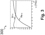
- the dielectric constant has complex values, and in Fig. 3 the real part Re ⁇ of the dielectric constant 300 and the imaginary part Im ⁇ of the dielectric constant 300 are depicted separately.
- the resonance frequency is advantageously located in the frequency range of the sub-THz to THz signal.
- the thickness h f of the ferroelectric layer may advantageously be selected to adjust the resonance frequency.
- a predefined maximum thickness of an individual layer of the heterostructure or a predefined maximum thickness of any of the layers of the heterostructure may be adjusted, for example to a value of 100 nm, in particular 70 nm or 40 nm.
- the resonance frequency can advantageously be matched to a frequency of the sub-THz to THz signal to achieve a strong and efficient coupling between the oscillation of the polarization pattern and the sub-THz to THz signal, for example by resonant coupling.
- a material of the ferroelectric layer 106 and a material of the dielectric layer 104 can advantageously be selected to adjust the resonance frequency v 0 .
- a static electric field and/or a mechanical stress can be applied to the heterostructure advantageously to adjust the resonance frequency v o .
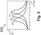
- Fig. 5 shows the dependence of the impedance amplitude
- the graph 500 gives the impedance amplitude
- has a maximum at a frequency similar or identical to the resonance frequency v o .
- the frequency-dependence of the impedance amplitude of the heterostructure is similar to the frequency-dependence of the impedance amplitude of well-known electronic components, like for example parallel LC resonant circuits.
- the heterostructure and the TFR 100 device may be employed in an electronic device like, for example, a signal receiver, a transmitter, or a processing device, operating in the frequency range of the sub-THz to THz signal, and the integration and application of the heterostructure and the TFR 100 device can advantageously make use of highly developed concepts for the integration and application of the well-known electronic components, like for example of the LC resonant circuit.
- the thickness h f of the ferroelectric layer may advantageously be selected to adjust the resonance frequency v o and consequently the frequency-dependence of the impedance amplitude, in particular the frequency at which the impedance amplitude has a maximum.
- the material of the ferroelectric layer 106 and the material of the dielectric layer 104 can advantageously be selected, and/or a static electric field and/or a mechanical stress can be applied to the heterostructure to adjust the resonance frequency ⁇ 0 .
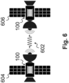
- Fig. 6 and Fig. 7 illustrate example applications, for which a signal receiver, transmitter, or processing device using a TFR 100 and operating in the frequency range of the sub-THz to THz signal may be particularly beneficial.
- a device employing a TFR 100 as a component of a transmitter and/or a receiver for a terahertz electromagnetic wave may find application in satellite communications.
- Terahertz electromagnetic waves 602 may be exchanged between a first satellite 604 and a second satellite 606, each comprising a transmitter and/or a receiver based on a TFR 100 .
- the space between the satellites is transparent in the terahertz spectral range to permit the propagation of the terahertz electromagnetic waves 602.
- the TFR 100 and in particular an integrated circuit with a TFR 100 may provide highly energy-efficient communication means for the first satellite 604 and the second satellite 606, in an environment where energy efficiency is particularly important.
- the TFR 100 also provides lightweight communication means, which can reduce the cost of launching the first satellite 604 and the second satellite 606 into space.
- resonant coupling between terahertz electromagnetic wave 602 and the TFR 100 provides frequency-selective communication means, suppressing noise from radiation at frequencies different from the resonance frequency of the TFR 100 . This advantage may be particularly important in a space environment, where radiation at various frequencies maybe abundant.
- a device employing a TFR 100 as a component of a transmitter and/or a receiver for a terahertz electromagnetic wave may form a basis for 6G WiFi communication 6G in this frequency range.
- the TFR 100 may be highly integrated with other electric components of an integrated electric circuit of a communication hub or an end user device 704, thus providing a cost-efficient communication technology for consumer products.
- the same or similar TFRs 100 in a single device may be used for coupling to the electromagnetic wave 702 on the one hand, and for electronic signal processing within the integrated circuit on the other.
- Both the communication hub and the end user device 704 may comprise integrated circuits each with one or multiple TFRs 100 .
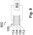
- the TFR 100 device is advantageously compatible with the integration into existing, miniaturized and highly developed semiconductor technology and integrated circuitry. Because of its small lateral area, the TFR 100 may be co-integrated with semiconductor devices such as diodes or transistors.
- Fig. 8 illustrates an integrated circuit 800 with a TFR 100 and a semiconductor device 802 according to an embodiment of the disclosure.
- a portion of the TFR 100 device may be processed, for example deposited or structured, in a single process step together with a portion of the semiconductor device 802.
- a layer of the TFR 100 such as a dielectric layer 104 , a ferroelectric layer 106, or a bottom electrode 112 and/or a top electrode 114 of the TFR 100 device may be deposited together with a similar layer of the semiconductor device 802 in a single deposition step.
- a layer of the TFR 100 device may be etched together with a layer of the semiconductor device in a single etching step.
- a layer of the TFR 100 device may be masked together with a layer of the semiconductor device in a single masking step.
- a driver circuit to drive the transmitter for the terahertz electromagnetic wave or a readout circuit to read the receiver for the terahertz electromagnetic wave may be implemented making use of a semiconductor device 802 such as a diode or a transistor.
- the heterostructure of the TFR 100 may be coupled to a diode or transistor 802, in particular to a gate of a transistor, to implement a rectifier converting the sub-THz to THz signal of the terahertz electromagnetic wave from an oscillation into a polar signal.
- Frequency-dependent properties of a TFR 100 device in particular the frequency-dependence of the impedance amplitude of the TFR 100, may advantageously be optimized for application in a specific device.
- the frequency-dependent impedance of a circuit comprising the TFR 100 device like, for example, an RC circuit, may be optimized by integrating additional electric components, like a load resistor, in the circuit.
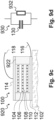
- a load resistor may either be implemented as a load resistor 900 integrated in series with the TFR 100 device as illustrated in Fig. 9a , or as a load resistor 920 integrated in parallel with the TFR as illustrated in Fig. 9c .
- Fig. 9b and Fig. 9d show the corresponding circuit diagrams 910, 930 with the electronic graphical symbol 130 of the TFR 100, a resistor in series 912, and a resistor in parallel 932.
- circuit according to the circuit diagram 910 of FIG. 9b may be achieved by forming an extended top electrode 114 or an extended bottom electrode 112 integrating with an additional resistive part 902 composed of one or several, metallic or semiconducting layers, whose thickness and material composition may be selected to optimize the resistance according to the requirements of the application in a specific device.
- circuit according to the circuit diagram 930 of Fig. 9d may be achieved by integrating a parallel load as a shunt-like structure, with a metallic or semiconducting shunt 922 connecting the top electrode 114 and bottom electrode 112.
- the metallic or semiconducting shunt 922 may be arranged between the top electrode 114 and bottom electrode 112 , or at least a portion of the metallic or semiconducting shunt 922 may be arranged outside the volume between the top electrode 114 and bottom electrode 112.
- Fig. 10 shows another example of an integrated circuit 1000 comprising two TFRs 100 .
- the TFR 100 can be co-integrated into a variety of integrated circuits. Additional examples of integrated circuits which may comprise and/or be based on the TFR 100 include a terahertz antenna, a transmitter and a receiver, which may also be referred to as a sensor of terahertz radiation.
- a device of an integrated circuit comprising the TFR 100 may be applied as a receiver to detect a sub-THz to THz signal emitted from another device of the integrated circuit.
- a device of an integrated circuit comprising the TFR 100 may be applied as a transmitter to generate a sub-THz to THz signal to be detected by another device of the integrated circuit.
- a transmitter based on the TFR 100 and a receiver based on the TFR 100 can be arranged on the same integrated circuit for the transmission, guiding, and/or manipulation of a sub-THz to THz signal.
- Fig. 10 shows an example of a corresponding integrated circuit 1000.
- the semiconductor devices 802 could, for example, correspond to a processor or a memory device.
- the TFR 100 may be used to establish a communication between the semiconductor devices 802 via a terahertz electromagnetic wave 1002.
- the terahertz electromagnetic wave 1002 may be an electromagnetic wave propagating freely in vacuum, gas, a dielectric or another form of matter, or it may be guided by a waveguide structure or it may be supported by a metallic channel, in particular by a plasmonic channel.
- the TFR 100 serves as a component of the integrated electric circuit, for example as a transmitter, receiver, or transceiver, but it may in addition serve as a terahertz optical device, which will be described in more detail later.
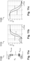
- Fig. 11a shows a circuit diagram 1100 corresponding to an embodiment of a frequency filter with a TFR 100 .
- a circuit according to the circuit diagram 1100 may be employed as a low pass filter, a high pass filter, or a bandpass filter.
- the high pass filter may be implemented by placing an input voltage, U in , across both the TFR 100, 130 and the resistor in series 912 as depicted in Fig. 11a .
- the TFR 100, 130 has an impedance Z TFR ( ⁇ ).
- the resistor in series 912 has a resistance R, which is essentially independent of frequency.
- the high pass filter may be completed by using as an output voltage U out,high a voltage across the resistor in series 912.
- Fig. 11b illustrates the frequency dependence of the output voltage U out,high 1110 of a high pass filter according to an embodiment of the disclosure.
- a low-pass filter is realized by the same circuit where the voltage output, U out , low , is taken from the TFR 130.
- the TFR 100 can also be employed in a terahertz optical device to guide the terahertz electromagnetic wave and/or manipulate its properties, like its amplitude, phase, direction, or (in case of pulsed terahertz electromagnetic radiation) pulse shape.
- the layered structure of the heterostructure of the TFR 100 can be used to tailor the TFR 100 to the requirements of a specific application, for example as a mirror, a beam splitter, an attenuator, a phase shifter, a dichroic mirror, a (terahertz) optical high pass filter, a (terahertz) optical low pass filter, a (terahertz) band pass filter, or a (terahertz) optical notch filter.
- the use of a device with the TFR 100 as a terahertz optical device may be combined with the use of the same device as an electronic resonator, for example as a receiver.
- a portion of the terahertz electromagnetic wave absorbed in the TFR 100 may be used for sensing, whereas another portion of the terahertz electromagnetic wave may be guided, reflected, or transmitted by the same TFR 100 serving as a terahertz optical device.
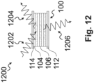
- Fig. 12 shows an example of a terahertz optical device 1200 with a TFR 100 to manipulate a terahertz electromagnetic wave according to an embodiment of the disclosure.
- the terahertz optical device 1200 may reflect a portion of an incident terahertz electromagnetic wave 1202 to generate a reflected terahertz electromagnetic wave 1204.
- the device may also transmit a portion of the incident terahertz electromagnetic wave 1202 to generate a transmitted terahertz electromagnetic wave 1206.
- the terahertz optical device 1200 may absorb a portion of the incident terahertz electromagnetic wave 1202.
- the terahertz optical device 1200 may use the portion of the incident terahertz electromagnetic wave 1202 absorbed by the device for electronic signal processing, for example for sensing the incident terahertz electromagnetic wave 1202.
- Fig. 13a and Fig. 13b illustrate the optical properties as a function of frequency v(THz) of a heterostructure according to an embodiment of the disclosure.
- Fig 13b gives the corresponding terahertz optical reflection coefficient R o for normal incidence.
- Properties of the layers of the heterostructure of the TFR 100 may be adjusted using the highly developed techniques for the design of layered dielectric optics.
- the properties of the layers of the heterostructure can be adjusted to achieve a desired amplitude, phase, or direction of the reflected terahertz electromagnetic wave 1204 and/or of the transmitted terahertz electromagnetic wave 1206.
- the thicknesses and the material compositions of the layers of the heterostructure may be adjusted.
- a static electric field and/or a mechanical stress can be applied to the heterostructure, constantly or dynamically (e.
- the terahertz optical device with a TFR 100 may, for example, advantageously be applied in wireless terahertz communication technologies or for on-chip wireless signal transmittance and processing. In some of these applications, it may be useful to adjust the thickness of the heterostructure to exceed or be comparable with the radiation wavelength. This may complicate the deposition of a bottom electrode 112 or a top electrode 114.
- the deposition of a top electrode 112 and/or a bottom electrode 114 may be omitted.
Landscapes
- Physics & Mathematics (AREA)
- General Physics & Mathematics (AREA)
- Optics & Photonics (AREA)
- Electromagnetism (AREA)
- Spectroscopy & Molecular Physics (AREA)
- Acoustics & Sound (AREA)
- Power Engineering (AREA)
- Theoretical Computer Science (AREA)
- Engineering & Computer Science (AREA)
- Semiconductor Integrated Circuits (AREA)
- Optical Modulation, Optical Deflection, Nonlinear Optics, Optical Demodulation, Optical Logic Elements (AREA)
- Control Of Motors That Do Not Use Commutators (AREA)
- Inorganic Insulating Materials (AREA)
- Compositions Of Oxide Ceramics (AREA)
- Piezo-Electric Or Mechanical Vibrators, Or Delay Or Filter Circuits (AREA)
- Lasers (AREA)
Claims (15)
- Verfahren zum Einsetzen einer Vorrichtung (100) als einen Resonator für Elektronen einer elektrischen Schaltung (800, 900, 920, 1000) oder für eine elektromagnetische Terahertzwelle (602, 702, 1002, 1202),
wobei die Vorrichtung Folgendes aufweist:eine Heterostruktur (200, 210);eine untere Elektrode (112), die unter der Heterostruktur (200, 210) angeordnet ist; undeine obere Elektrode (114), die über der Heterostruktur (200, 210) angeordnet ist;wobei:
die Heterostruktur (200, 210) aufweist: eine Mehrzahl von dielektrischen Schichten (104), eine Mehrzahl von ferroelektrischen Schichten (106) und eine alternierende Stapelfolge der dielektrischen Schichten der Vielzahl von dielektrischen Schichten (104) und der ferroelektrischen Schichten der Vielzahl von ferroelektrischen Schichten (106), wobei:die ferroelektrischen Schichten (106) jeweils eine Mehrzahlen von ferroelektrischen Polarisationsdomänen (108, 110) aufweisen, die Polarisationsmuster bilden, und die Polarisationsmuster dazu eingerichtet sind, um Oszillationen mit Resonanzfrequenzen in einem Terahertz-Frequenzbereich durchzuführen;wobei das Verfahren umfasst:
funktionelles Koppeln der Oszillationen des Polarisationsmusters und einer Oszillation der Elektronen der elektrischen Schaltung (800, 900, 920, 1000) oder der elektromagnetischen Terahertzwelle (602, 702, 1002, 1202) durch die Vorrichtung (100). - Verfahren nach Anspruch 1, das ferner ein Einsetzen der Vorrichtung (100) als eine Komponente eines Empfängers oder eines Senders für die elektromagnetische Terahertzwelle (602, 702, 1002, 1202) umfasst.
- Verfahren nach einem der vorhergehenden Ansprüche, das ferner ein Anwenden der Vorrichtung (100) als eine Komponente einer RC-Schaltung (900, 920) umfasst.
- Verfahren nach einem der vorhergehenden Ansprüche, das ferner umfasst:
Einsetzen der Vorrichtung (100) als eine Komponente eines Tiefpassfilters (1100, 1120), eines Hochpassfilters (1100, 1110) oder eines Bandpassfilters. - Verfahren nach einem der vorhergehenden Ansprüche, das ferner umfasst:
Verwenden der Vorrichtung (100) als eine Komponente eines Zeitsignalgebers. - Verfahren nach einem der vorhergehenden Ansprüche, wobei die Vorrichtung (100) ferner eine zweite Heterostruktur (200, 210) aufweist, die mindestens eine zweite dielektrische Schicht (104) und mindestens eine zweite ferroelektrische Schicht (106) aufweist, wobei die mindestens eine zweite ferroelektrische Schicht (106) eine zweite Mehrzahl von ferroelektrischen Polarisationsdomänen (108, 110) aufweist, die ein zweites Polarisationsmuster bilden, und wobei das zweite Polarisationsmuster dazu eingerichtet ist, um eine zweite Oszillation mit einer zweiten Resonanzfrequenz in dem Terahertz-Frequenzbereich durchzuführen;
wobei das Anwenden der Vorrichtung (100) ferner umfasst:Einsetzen der Heterostruktur (200, 210) als eine Komponente eines Senders, der dazu eingerichtet ist, um eine transiente elektromagnetische Terahertzwelle (602, 702, 1002) zu erzeugen; undEinsetzen der zweiten Heterostruktur (200, 210) als eine Komponente eines Empfängers, um die transiente elektromagnetische Terahertzwelle (602, 702, 1002, 1202) zu empfangen. - Verfahren nach einem der vorhergehenden Ansprüche, das ferner umfasst:
Verwenden der Vorrichtung (100) als eine Komponente einer optischen Terahertzvorrichtung (100), um die elektromagnetische Terahertzwelle (1202,1204, 1206) zu manipulieren und um mindestens einen optischen Terahertzparameter zu steuern. - Vorrichtung (100), die dafür eingerichtet ist, als ein Resonator für Elektronen einer elektrischen Schaltung (800, 900, 920, 1000) oder für eine elektromagnetische Terahertzwelle (602, 702, 1002, 1202) angewendet zu werden, wobei die Vorrichtung umfasst:eine Heterostruktur (200, 210);eine untere Elektrode (112), die unter der Heterostruktur (200, 210) angeordnet ist; undeine obere Elektrode (114), die über der Heterostruktur (200, 210) angeordnet ist;wobei:
die Heterostruktur (200, 210) aufweist: eine Mehrzahl von dielektrischen Schichten (104), eine Mehrzahl von ferroelektrischen Schichten (106) und eine alternierende Stapelfolge der dielektrischen Schichten der Mehrzahl von dielektrischen Schichten (104) und der ferroelektrischen Schichten der Mehrzahl von ferroelektrischen Schichten (106), wobei:die ferroelektrischen Schichten (106) jeweils eine Mehrzahl von ferroelektrischen Polarisationsdomänen (108, 110) aufweisen, die Polarisationsmuster bilden, unddie Polarisationsmuster dazu eingerichtet sind, um Oszillationen mit Resonanzfrequenzen in einem Terahertz-Frequenzbereich durchzuführen;wobei die Vorrichtung (100) dazu eingerichtet ist, um die Oszillationen der Polarisationsmuster mit einer Oszillation bei einer Kopplungsfrequenz der Elektronen der elektrischen Schaltung (800, 900, 920, 1000) oder der elektromagnetischen Terahertzwelle (602, 702, 1002, 1202) zu koppeln, wobei die Oszillationen der Polarisationsmuster Oszillationsfrequenzen in dem Terahertz-Frequenzbereich aufweisen. - Vorrichtung (100) nach Anspruch 8, wobei die Heterostruktur (200, 210) über einem Substrat (102) angeordnet ist, wobei das Substrat (102) dazu eingerichtet ist, um ein epitaktisches Wachstum von mindestens einer dielektrischen Schicht (104) der Mehrzahl von dielektrischen Schichten oder von mindestens einer ferroelektrischen Schicht (106) der Mehrzahl von ferroelektrischen Schichten zu begünstigen.
- Vorrichtung (100) nach einem der Ansprüche 8 oder 9, die ferner eine Zwischenelektrode umfasst, die zwischen einer oberen Zwischenschicht und einer unteren Zwischenschicht angeordnet ist, wobei die obere Zwischenschicht und die untere Zwischenschicht dielektrische Schichten (104) aus der Mehrzahl von dielektrischen Schichten sind.
- Vorrichtung (100) nach einem der Ansprüche 8 bis 10, die ferner ein zusätzliches integriertes Element (802, 902, 922) umfasst, wobei die Heterostruktur (200, 210) eine erste Komponente einer gemeinsamen integrierten Schaltung (800, 900, 920, 1000) ist und das zusätzliche integrierte Element (802, 902, 922) eine zweite Komponente der gemeinsamen integrierten Schaltung (800, 900, 920, 1000) ist.
- Vorrichtung nach Anspruch 11, wobei das zusätzliche integrierte Element (802) eine Diode oder ein Transistor ist und die Vorrichtung eine Komponente eines Empfängers oder eines Senders ist.
- Vorrichtung nach Anspruch 11 oder 12, wobei das zusätzliche integrierte Element (902, 922) ein Widerstand ist und wobei die Heterostruktur und der Widerstand in direktem physischem Kontakt miteinander ausgebildet sind.
- Vorrichtung (100) nach einem der Ansprüche 8 bis 13, die ferner eine zweite Heterostruktur (200, 210) umfasst, die dafür eingerichtet ist, als ein zweiter Resonator für Elektronen einer zweiten elektrischen Schaltung oder für eine zweite elektromagnetische Terahertzwelle angewendet zu werden, wobei:
die zweite Heterostruktur (200, 210) mindestens eine zweite dielektrische Schicht (104) und mindestens eine zweite ferroelektrische Schicht (106) aufweist, wobei:die mindestens eine zweite ferroelektrische Schicht (106) eine zweite Mehrzahl von ferroelektrischen Polarisationsdomänen (108, 110) aufweist, die ein zweites Polarisationsmuster bilden, unddas zweite Polarisationsmuster dazu eingerichtet ist, um eine zweite Oszillation mit einer zweiten Resonanzfrequenz in dem Terahertz-Frequenzbereich durchzuführen;wobei die Vorrichtung (100) dazu eingerichtet ist, um die zweite Oszillation des zweiten Polarisationsmusters mit einer dritten Oszillation bei einer zweiten Kopplungsfrequenz der Elektronen der zweiten elektrischen Schaltung oder der zweiten elektromagnetischen Terahertzwelle zu koppeln, wobei die zweite Oszillation des zweiten Polarisationsmusters eine zweite Oszillationsfrequenz in dem Terahertz-Frequenzbereich aufweist. - Verfahren zum Herstellen einer Vorrichtung (100), die dafür eingerichtet ist, als ein Resonator für Elektronen einer elektrischen Schaltung (800, 900, 920, 1000) oder für eine elektromagnetische Terahertzwelle (602, 702, 1002, 1202) angewendet zu werden, wobei die Vorrichtung eine Heterostruktur (200, 210) und eine untere Elektrode (112), die unter der Heterostruktur (200, 210) angeordnet ist, umfasst; wobei das Verfahren umfasst:Abscheiden der unteren Elektrode (112) über einem Substrat (102);Abscheiden einer Mehrzahl von ferroelektrischen Schichten (106) der Heterostruktur (200, 210) und einer Mehrzahl von dielektrischen Schichten (104) der Heterostruktur (200, 210) mit einer alternierenden Stapelfolge der dielektrischen Schichten der Mehrzahl von dielektrischen Schichten (104) und der ferroelektrischen Schichten der Mehrzahl von ferroelektrischen Schichten (106), undHerstellen einer oberen Elektrode (114) über der Heterostruktur (200, 210);wobei Ferroelektrikschicht-Dicken (hf) der ferroelektrischen Schichten (106) der Mehrzahl von ferroelektrischen Schichten (106) eine vordefinierte maximale Dicke nicht überschreiten,so dass die ferroelektrischen Schichten (106) der Mehrzahl von ferroelektrischen Schichten (106) jeweils eine Mehrzahl von ferroelektrischen Polarisationsdomänen (108, 110) aufweisen, die Polarisationsmuster bilden, die dazu eingerichtet sind, um Oszillationen mit Resonanzfrequenzen durchzuführen, undEinstellen der vordefinierten maximalen Dicke auf eine Resonanzfrequenz in einem Terahertz-Frequenzbereich.
Priority Applications (8)
| Application Number | Priority Date | Filing Date | Title |
|---|---|---|---|
| EP21160551.4A EP4054074B8 (de) | 2021-03-03 | 2021-03-03 | Ferroelektrischer terahertz-resonator |
| AU2022200893A AU2022200893B2 (en) | 2021-03-03 | 2022-02-10 | Terahertz ferroelectric resonator |
| JP2022029350A JP2022135993A (ja) | 2021-03-03 | 2022-02-28 | テラヘルツ強誘電共振器 |
| KR1020220026631A KR102702235B1 (ko) | 2021-03-03 | 2022-03-02 | 테라헤르츠 강유전체 공진기 |
| CN202210199906.5A CN115037273A (zh) | 2021-03-03 | 2022-03-02 | 太赫兹铁电谐振器 |
| US17/685,996 US11803002B2 (en) | 2021-03-03 | 2022-03-03 | Device with a heterostructure adapted to be applied as a resonator for electrons of an electrical circuit or for a terahertz electromagnetic wave |
| CA3151159A CA3151159C (en) | 2021-03-03 | 2022-03-03 | TERAHERTZ FERROELECTRIC RESONATOR |
| JP2024162265A JP7774339B2 (ja) | 2021-03-03 | 2024-09-19 | テラヘルツ強誘電共振器 |
Applications Claiming Priority (1)
| Application Number | Priority Date | Filing Date | Title |
|---|---|---|---|
| EP21160551.4A EP4054074B8 (de) | 2021-03-03 | 2021-03-03 | Ferroelektrischer terahertz-resonator |
Publications (4)
| Publication Number | Publication Date |
|---|---|
| EP4054074A1 EP4054074A1 (de) | 2022-09-07 |
| EP4054074B1 true EP4054074B1 (de) | 2024-12-18 |
| EP4054074C0 EP4054074C0 (de) | 2024-12-18 |
| EP4054074B8 EP4054074B8 (de) | 2025-02-12 |
Family
ID=74858225
Family Applications (1)
| Application Number | Title | Priority Date | Filing Date |
|---|---|---|---|
| EP21160551.4A Active EP4054074B8 (de) | 2021-03-03 | 2021-03-03 | Ferroelektrischer terahertz-resonator |
Country Status (7)
| Country | Link |
|---|---|
| US (1) | US11803002B2 (de) |
| EP (1) | EP4054074B8 (de) |
| JP (2) | JP2022135993A (de) |
| KR (1) | KR102702235B1 (de) |
| CN (1) | CN115037273A (de) |
| AU (1) | AU2022200893B2 (de) |
| CA (1) | CA3151159C (de) |
Families Citing this family (2)
| Publication number | Priority date | Publication date | Assignee | Title |
|---|---|---|---|---|
| US20230134722A1 (en) * | 2021-10-28 | 2023-05-04 | Texas Instruments Incorporated | Monolithic ultrasonic flow meter and particle detection system |
| WO2025186863A1 (en) * | 2024-03-04 | 2025-09-12 | Ntt, Inc. | Electrostrictive element |
Family Cites Families (14)
| Publication number | Priority date | Publication date | Assignee | Title |
|---|---|---|---|---|
| CN1326600A (zh) * | 1998-10-16 | 2001-12-12 | 帕拉泰克微波公司 | 用于微波用途的电压可调谐分层介电材料 |
| JP2001220300A (ja) * | 2000-02-14 | 2001-08-14 | Murata Mfg Co Ltd | 酸化物超格子およびその製造方法 |
| US7272158B1 (en) * | 2005-02-15 | 2007-09-18 | Hrl Laboratories, Llc | Highly efficient waveguide pulsed THz electromagnetic radiation source and group-matched waveguide THz electromagnetic radiation source |
| DE102005044330A1 (de) * | 2005-09-16 | 2007-03-29 | Epcos Ag | Abstimmbarer Kondensator und Schaltung mit einem solchen Kondensator |
| US20080107885A1 (en) * | 2006-07-12 | 2008-05-08 | Alpay S P | High-capacity, low-leakage multilayer dielectric stacks |
| JP2009026994A (ja) * | 2007-07-20 | 2009-02-05 | Rohm Co Ltd | 強誘電体材料およびその製造方法 |
| US7898158B1 (en) * | 2007-11-01 | 2011-03-01 | Rf Micro Devices, Inc. | MEMS vibrating structure using a single-crystal piezoelectric thin-film layer having domain inversions |
| JP2012165032A (ja) * | 2009-04-30 | 2012-08-30 | Murata Mfg Co Ltd | 弾性波装置 |
| US8507860B2 (en) * | 2009-05-20 | 2013-08-13 | Nutech Ventures | Terahertz resonator |
| CN103178351B (zh) * | 2013-02-27 | 2016-08-10 | 华中科技大学 | 一种频率可调的太赫兹波超材料调制器 |
| US10594261B2 (en) * | 2016-07-19 | 2020-03-17 | Board Of Regents, The University Of Texas Systems | Piezoelectric resonance controlled terahertz wave modulators |
| EP3602188B1 (de) * | 2017-03-21 | 2023-07-12 | ETH Zürich | Vorrichtung zur thz-erzeugung und/oder -detektion und verfahren zur herstellung davon |
| US10615669B2 (en) * | 2018-01-12 | 2020-04-07 | Littelfuse, Inc. | Protection device and system using negative capacitance component |
| US11605624B2 (en) * | 2019-01-02 | 2023-03-14 | Intel Corporation | Ferroelectric resonator |
-
2021
- 2021-03-03 EP EP21160551.4A patent/EP4054074B8/de active Active
-
2022
- 2022-02-10 AU AU2022200893A patent/AU2022200893B2/en active Active
- 2022-02-28 JP JP2022029350A patent/JP2022135993A/ja active Pending
- 2022-03-02 CN CN202210199906.5A patent/CN115037273A/zh active Pending
- 2022-03-02 KR KR1020220026631A patent/KR102702235B1/ko active Active
- 2022-03-03 CA CA3151159A patent/CA3151159C/en active Active
- 2022-03-03 US US17/685,996 patent/US11803002B2/en active Active
-
2024
- 2024-09-19 JP JP2024162265A patent/JP7774339B2/ja active Active
Also Published As
| Publication number | Publication date |
|---|---|
| US20220283348A1 (en) | 2022-09-08 |
| KR20220124644A (ko) | 2022-09-14 |
| AU2022200893A1 (en) | 2022-09-22 |
| EP4054074B8 (de) | 2025-02-12 |
| JP2024169596A (ja) | 2024-12-05 |
| US11803002B2 (en) | 2023-10-31 |
| AU2022200893B2 (en) | 2023-09-14 |
| JP7774339B2 (ja) | 2025-11-21 |
| CA3151159C (en) | 2025-06-17 |
| KR102702235B1 (ko) | 2024-09-02 |
| EP4054074C0 (de) | 2024-12-18 |
| CN115037273A (zh) | 2022-09-09 |
| EP4054074A1 (de) | 2022-09-07 |
| JP2022135993A (ja) | 2022-09-15 |
| CA3151159A1 (en) | 2022-09-03 |
Similar Documents
| Publication | Publication Date | Title |
|---|---|---|
| JP7774339B2 (ja) | テラヘルツ強誘電共振器 | |
| EP2122743B1 (de) | Bandpassfilter und verfahren zu seiner herstellung | |
| US7804383B2 (en) | Coupled lamb wave resonators filter | |
| EP4033660A1 (de) | Volumenwellenresonator mit anpassungsschicht sowie filter und elektronische vorrichtung | |
| US7170370B2 (en) | Filter device capable of obtaining attenuation characteristic of sharpness in narrow band width and branching filter using the same | |
| US7689390B2 (en) | Method of modeling electrostrictive effects and acoustic resonances in a tunable capacitor | |
| US11257762B2 (en) | High speed semiconductor chip stack | |
| TW202324921A (zh) | 體聲波共振器濾波器以及體聲波共振器濾波器模組 | |
| US7242130B2 (en) | Piezoelectric device, antenna duplexer, and method of manufacturing piezoelectric resonators used therefor | |
| US7304551B2 (en) | Branching filter and communication device | |
| US20230179172A1 (en) | Acoustic resonator filter and acoustic resonator package | |
| US20250211201A1 (en) | Bulk acoustic wave filter device | |
| US20240030888A1 (en) | Substrate for surface acoustic wave device and surface acoustic wave device comprising the same | |
| KR20220120475A (ko) | 집적 수동 디바이스 상에 적층되는 벌크 탄성파 공명기 | |
| CN114189225A (zh) | 一种薄膜体声波谐振器及应用其的滤波器 | |
| US20240364299A1 (en) | Bulk acoustic resonator | |
| US20230084640A1 (en) | Acoustic resonator package | |
| CN118249767A (zh) | 体声波谐振器及其制备方法、电子设备 | |
| US20070007850A1 (en) | Apparatus and method capable of a high fundamental acoustic resonance frequency and a wide resonance-free frequency range | |
| CN121794890A (zh) | 声学谐振器和声学谐振器的制造方法 | |
| JP2005093465A (ja) | 薄膜キャパシタ、圧電フィルタおよびその製造方法、ならびに分波器、通信機 | |
| Mansour | Switchable and Tunable Bulk Acoustic Wave Devices Based on Ferroelectric Material | |
| JP2005243965A (ja) | 可変容量素子 |
Legal Events
| Date | Code | Title | Description |
|---|---|---|---|
| PUAI | Public reference made under article 153(3) epc to a published international application that has entered the european phase |
Free format text: ORIGINAL CODE: 0009012 |
|
| STAA | Information on the status of an ep patent application or granted ep patent |
Free format text: STATUS: THE APPLICATION HAS BEEN PUBLISHED |
|
| STAA | Information on the status of an ep patent application or granted ep patent |
Free format text: STATUS: REQUEST FOR EXAMINATION WAS MADE |
|
| AK | Designated contracting states |
Kind code of ref document: A1 Designated state(s): AL AT BE BG CH CY CZ DE DK EE ES FI FR GB GR HR HU IE IS IT LI LT LU LV MC MK MT NL NO PL PT RO RS SE SI SK SM TR |
|
| 17P | Request for examination filed |
Effective date: 20220826 |
|
| RBV | Designated contracting states (corrected) |
Designated state(s): AL AT BE BG CH CY CZ DE DK EE ES FI FR GB GR HR HU IE IS IT LI LT LU LV MC MK MT NL NO PL PT RO RS SE SI SK SM TR |
|
| RIN1 | Information on inventor provided before grant (corrected) |
Inventor name: VINOKOUR, VALERII Inventor name: RAZUMNAYA, ANNA Inventor name: LUKYANCHUK, IGOR |
|
| GRAP | Despatch of communication of intention to grant a patent |
Free format text: ORIGINAL CODE: EPIDOSNIGR1 |
|
| STAA | Information on the status of an ep patent application or granted ep patent |
Free format text: STATUS: GRANT OF PATENT IS INTENDED |
|
| INTG | Intention to grant announced |
Effective date: 20240712 |
|
| GRAS | Grant fee paid |
Free format text: ORIGINAL CODE: EPIDOSNIGR3 |
|
| GRAA | (expected) grant |
Free format text: ORIGINAL CODE: 0009210 |
|
| STAA | Information on the status of an ep patent application or granted ep patent |
Free format text: STATUS: THE PATENT HAS BEEN GRANTED |
|
| REG | Reference to a national code |
Ref country code: DE Ref legal event code: R081 Ref document number: 602021023414 Country of ref document: DE Owner name: TERRA QUANTUM AG, CH Free format text: FORMER OWNER: TERRA QUANTUM AG, RORSCHACH, CH |
|
| AK | Designated contracting states |
Kind code of ref document: B1 Designated state(s): AL AT BE BG CH CY CZ DE DK EE ES FI FR GB GR HR HU IE IS IT LI LT LU LV MC MK MT NL NO PL PT RO RS SE SI SK SM TR |
|
| REG | Reference to a national code |
Ref country code: CH Ref legal event code: EP |
|
| RAP4 | Party data changed (patent owner data changed or rights of a patent transferred) |
Owner name: TERRA QUANTUM AG |
|
| REG | Reference to a national code |
Ref country code: DE Ref legal event code: R096 Ref document number: 602021023414 Country of ref document: DE |
|
| REG | Reference to a national code |
Ref country code: IE Ref legal event code: FG4D Ref country code: CH Ref legal event code: PK Free format text: BERICHTIGUNG B8 |
|
| U01 | Request for unitary effect filed |
Effective date: 20241218 |
|
| U07 | Unitary effect registered |
Designated state(s): AT BE BG DE DK EE FI FR IT LT LU LV MT NL PT RO SE SI Effective date: 20250102 |
|
| REG | Reference to a national code |
Ref country code: CH Ref legal event code: PK Free format text: BERICHTIGUNGEN |
|
| RIN2 | Information on inventor provided after grant (corrected) |
Inventor name: VINOKOUR, VALERII Inventor name: RAZUMNAYA, ANNA Inventor name: LUKYANCHUK, IGOR |
|
| U1N | Appointed representative for the unitary patent procedure changed after the registration of the unitary effect |
Representative=s name: LUCKE, ANDREAS; DE |
|
| PG25 | Lapsed in a contracting state [announced via postgrant information from national office to epo] |
Ref country code: HR Free format text: LAPSE BECAUSE OF FAILURE TO SUBMIT A TRANSLATION OF THE DESCRIPTION OR TO PAY THE FEE WITHIN THE PRESCRIBED TIME-LIMIT Effective date: 20241218 |
|
| PG25 | Lapsed in a contracting state [announced via postgrant information from national office to epo] |
Ref country code: NO Free format text: LAPSE BECAUSE OF FAILURE TO SUBMIT A TRANSLATION OF THE DESCRIPTION OR TO PAY THE FEE WITHIN THE PRESCRIBED TIME-LIMIT Effective date: 20250318 |
|
| PG25 | Lapsed in a contracting state [announced via postgrant information from national office to epo] |
Ref country code: GR Free format text: LAPSE BECAUSE OF FAILURE TO SUBMIT A TRANSLATION OF THE DESCRIPTION OR TO PAY THE FEE WITHIN THE PRESCRIBED TIME-LIMIT Effective date: 20250319 |
|
| PGFP | Annual fee paid to national office [announced via postgrant information from national office to epo] |
Ref country code: GB Payment date: 20250326 Year of fee payment: 5 |
|
| PG25 | Lapsed in a contracting state [announced via postgrant information from national office to epo] |
Ref country code: RS Free format text: LAPSE BECAUSE OF FAILURE TO SUBMIT A TRANSLATION OF THE DESCRIPTION OR TO PAY THE FEE WITHIN THE PRESCRIBED TIME-LIMIT Effective date: 20250318 |
|
| U20 | Renewal fee for the european patent with unitary effect paid |
Year of fee payment: 5 Effective date: 20250325 |
|
| PG25 | Lapsed in a contracting state [announced via postgrant information from national office to epo] |
Ref country code: SM Free format text: LAPSE BECAUSE OF FAILURE TO SUBMIT A TRANSLATION OF THE DESCRIPTION OR TO PAY THE FEE WITHIN THE PRESCRIBED TIME-LIMIT Effective date: 20241218 |
|
| PG25 | Lapsed in a contracting state [announced via postgrant information from national office to epo] |
Ref country code: PL Free format text: LAPSE BECAUSE OF FAILURE TO SUBMIT A TRANSLATION OF THE DESCRIPTION OR TO PAY THE FEE WITHIN THE PRESCRIBED TIME-LIMIT Effective date: 20241218 |
|
| PG25 | Lapsed in a contracting state [announced via postgrant information from national office to epo] |
Ref country code: ES Free format text: LAPSE BECAUSE OF FAILURE TO SUBMIT A TRANSLATION OF THE DESCRIPTION OR TO PAY THE FEE WITHIN THE PRESCRIBED TIME-LIMIT Effective date: 20241218 |
|
| PG25 | Lapsed in a contracting state [announced via postgrant information from national office to epo] |
Ref country code: IS Free format text: LAPSE BECAUSE OF FAILURE TO SUBMIT A TRANSLATION OF THE DESCRIPTION OR TO PAY THE FEE WITHIN THE PRESCRIBED TIME-LIMIT Effective date: 20250418 |
|
| PGFP | Annual fee paid to national office [announced via postgrant information from national office to epo] |
Ref country code: CH Payment date: 20250401 Year of fee payment: 5 |
|
| PG25 | Lapsed in a contracting state [announced via postgrant information from national office to epo] |
Ref country code: SK Free format text: LAPSE BECAUSE OF FAILURE TO SUBMIT A TRANSLATION OF THE DESCRIPTION OR TO PAY THE FEE WITHIN THE PRESCRIBED TIME-LIMIT Effective date: 20241218 |
|
| PG25 | Lapsed in a contracting state [announced via postgrant information from national office to epo] |
Ref country code: CZ Free format text: LAPSE BECAUSE OF FAILURE TO SUBMIT A TRANSLATION OF THE DESCRIPTION OR TO PAY THE FEE WITHIN THE PRESCRIBED TIME-LIMIT Effective date: 20241218 |
|
| PG25 | Lapsed in a contracting state [announced via postgrant information from national office to epo] |
Ref country code: MC Free format text: LAPSE BECAUSE OF FAILURE TO SUBMIT A TRANSLATION OF THE DESCRIPTION OR TO PAY THE FEE WITHIN THE PRESCRIBED TIME-LIMIT Effective date: 20241218 |
|
| PLBE | No opposition filed within time limit |
Free format text: ORIGINAL CODE: 0009261 |
|
| STAA | Information on the status of an ep patent application or granted ep patent |
Free format text: STATUS: NO OPPOSITION FILED WITHIN TIME LIMIT |
|
| 26N | No opposition filed |
Effective date: 20250919 |
|
| PG25 | Lapsed in a contracting state [announced via postgrant information from national office to epo] |
Ref country code: IE Free format text: LAPSE BECAUSE OF NON-PAYMENT OF DUE FEES Effective date: 20250303 |