EP4050754B1 - Power supply system, and electronic device - Google Patents
Power supply system, and electronic device Download PDFInfo
- Publication number
- EP4050754B1 EP4050754B1 EP21890369.8A EP21890369A EP4050754B1 EP 4050754 B1 EP4050754 B1 EP 4050754B1 EP 21890369 A EP21890369 A EP 21890369A EP 4050754 B1 EP4050754 B1 EP 4050754B1
- Authority
- EP
- European Patent Office
- Prior art keywords
- switch
- switch circuit
- coupled
- cell group
- circuit
- Prior art date
- Legal status (The legal status is an assumption and is not a legal conclusion. Google has not performed a legal analysis and makes no representation as to the accuracy of the status listed.)
- Active
Links
- 239000003990 capacitor Substances 0.000 claims description 57
- 230000002159 abnormal effect Effects 0.000 claims description 8
- 238000000034 method Methods 0.000 description 72
- 230000008569 process Effects 0.000 description 48
- 238000010586 diagram Methods 0.000 description 35
- 238000004891 communication Methods 0.000 description 19
- 230000006870 function Effects 0.000 description 19
- 238000007726 management method Methods 0.000 description 19
- 238000012545 processing Methods 0.000 description 15
- 238000010295 mobile communication Methods 0.000 description 12
- 238000004590 computer program Methods 0.000 description 10
- 230000005236 sound signal Effects 0.000 description 9
- 230000001960 triggered effect Effects 0.000 description 9
- 229920001621 AMOLED Polymers 0.000 description 6
- 230000003287 optical effect Effects 0.000 description 4
- 238000013500 data storage Methods 0.000 description 3
- 238000013461 design Methods 0.000 description 3
- 238000005516 engineering process Methods 0.000 description 3
- 238000010438 heat treatment Methods 0.000 description 3
- 230000009467 reduction Effects 0.000 description 3
- 239000004065 semiconductor Substances 0.000 description 3
- 238000013528 artificial neural network Methods 0.000 description 2
- 230000003416 augmentation Effects 0.000 description 2
- 238000004422 calculation algorithm Methods 0.000 description 2
- 230000001413 cellular effect Effects 0.000 description 2
- 230000000295 complement effect Effects 0.000 description 2
- 230000003111 delayed effect Effects 0.000 description 2
- 238000011161 development Methods 0.000 description 2
- 238000007599 discharging Methods 0.000 description 2
- 230000000694 effects Effects 0.000 description 2
- 239000004973 liquid crystal related substance Substances 0.000 description 2
- 230000007774 longterm Effects 0.000 description 2
- 238000005457 optimization Methods 0.000 description 2
- 239000002096 quantum dot Substances 0.000 description 2
- 230000004044 response Effects 0.000 description 2
- 239000007787 solid Substances 0.000 description 2
- 230000001133 acceleration Effects 0.000 description 1
- 230000009286 beneficial effect Effects 0.000 description 1
- 210000000988 bone and bone Anatomy 0.000 description 1
- 238000004364 calculation method Methods 0.000 description 1
- 230000008859 change Effects 0.000 description 1
- 238000006243 chemical reaction Methods 0.000 description 1
- 230000001419 dependent effect Effects 0.000 description 1
- 230000005611 electricity Effects 0.000 description 1
- 230000003862 health status Effects 0.000 description 1
- 238000003780 insertion Methods 0.000 description 1
- 230000037431 insertion Effects 0.000 description 1
- 239000013307 optical fiber Substances 0.000 description 1
- 230000000007 visual effect Effects 0.000 description 1
Images


Classifications
-
- H—ELECTRICITY
- H02—GENERATION; CONVERSION OR DISTRIBUTION OF ELECTRIC POWER
- H02J—CIRCUIT ARRANGEMENTS OR SYSTEMS FOR SUPPLYING OR DISTRIBUTING ELECTRIC POWER; SYSTEMS FOR STORING ELECTRIC ENERGY
- H02J7/00—Circuit arrangements for charging or depolarising batteries or for supplying loads from batteries
- H02J7/0013—Circuit arrangements for charging or depolarising batteries or for supplying loads from batteries acting upon several batteries simultaneously or sequentially
- H02J7/0024—Parallel/serial switching of connection of batteries to charge or load circuit
-
- H—ELECTRICITY
- H02—GENERATION; CONVERSION OR DISTRIBUTION OF ELECTRIC POWER
- H02J—CIRCUIT ARRANGEMENTS OR SYSTEMS FOR SUPPLYING OR DISTRIBUTING ELECTRIC POWER; SYSTEMS FOR STORING ELECTRIC ENERGY
- H02J7/00—Circuit arrangements for charging or depolarising batteries or for supplying loads from batteries
- H02J7/0013—Circuit arrangements for charging or depolarising batteries or for supplying loads from batteries acting upon several batteries simultaneously or sequentially
- H02J7/0014—Circuits for equalisation of charge between batteries
- H02J7/0019—Circuits for equalisation of charge between batteries using switched or multiplexed charge circuits
Definitions
- Embodiments of this application relates to the field of power supplies, and in particular, to a power supply system, and an electronic device.
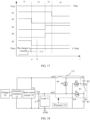
- FIG. 1 provides a buck charging solution, generally, a system rated voltage Vbat of a mobile phone does not exceed 6 V, and a plurality of cells in a mobile phone battery (the voltage of a single cell is 3-4 V) are connected in parallel to directly supply power to a load.
- the voltage outputted from the charger to an external interface of the mobile phone is 2-4 times of the voltage of the cell.
- FIG. 2 provides a buck power supply solution.
- a plurality of cells the voltage of a single cell is 3-4 V
- the voltage of two cells connected in series may reach up to 6-8 V
- the voltage outputted from the charger to an external interface of the mobile phone for example, a USB interface
- the loss caused by the buck switch circuit may lead to excessive heating of the mobile phone during charging and affect the charging efficiency of the mobile phone; and in the buck power supply solution, part of the capacity of the cells may be lost in the form of heat consumption during the buck process of the buck switch circuit, which leads to shorter standby time of the mobile phone.
- KR-A-20200117817 describes a power management device, the device includes two power nodes selectively connected to a first power source or a second power source, a first power source providing a first voltage and a second power supply providing a second voltage lower than the first voltage using a battery including a plurality of cells.
- the power management device for managing power of a system operating by receiving power, and charging the plurality of cells by connecting the plurality of cells in series in a high voltage mode operating by receiving a first voltage from the first power source, and in a low voltage mode operating by receiving a second voltage from the second power source, the power management device charges the plurality of cells by connecting the plurality cells in parallel.
- the power management device in a battery mode operating in a state in which power is not supplied from any of the plurality of power sources, connectes the plurality of cells in parallel and discharges the plurality of cells to power the load of the system.
- WO-A1-2020/199833 describes a charging and discharging circuit for a mobile terminal using a multi-cell battery, the circuit is configured to switch each battery cell in the multi-cell battery to a serial state and connect it to the battery connector when the multi-cell battery is charging; when the multi-cell battery is not charging, switching each battery cell in the multi-cell battery to a parallel state and connecting it to the battery connector.
- a power supply system according to claim 1.
- Embodiments of the invention are defined in the dependent claims.
- An example in this application but not part of the invention provides a method for switching a connection status of a cell, a power supply system, and an electronic device, which can switch the connection status of a cell group to be serially-connected when charging the cell group, and switch the connection status of the cell group to be parallelly-connected when the cell group supplies power to a load, so as to improve charging efficiency and reduce heat loss when the cell group supplies power.
- a first aspect of this disclosure provides a power supply system, applicable to an electronic device.
- the electronic device includes at least two cell groups, an external interface, and a load, where each of the cell groups includes at least one cell, and the at least one cell is coupled between two poles of the cell group.
- the power supply system includes a toggle switch circuit and a buck switch circuit.
- the toggle switch circuit includes a first output end, a second output end, and a plurality of input ends. Two poles of the cell group are each coupled to an input end of the toggle switch circuit.
- the first output end of the toggle switch circuit is coupled to an input end of the buck switch circuit
- the second output end of the toggle switch circuit is coupled to an output end of the buck switch circuit
- the input end of the buck switch circuit is coupled to an external interface.
- the output end of the buck switch circuit is further coupled to the load, and the external interface is configured to connect a charger.
- the toggle switch circuit is configured to switch a connection status of at least two cell groups to be serially-connected or parallelly-connected.
- the toggle switch circuit is configured to switch the connection status of the at least two cell groups to be serially-connected, so that the at least two cell groups are connected in series between the first output end of the toggle switch circuit and a grounding end, and the buck switch circuit is configured to adjust a voltage of the charger to a system rated voltage and output the voltage to the output end of the buck switch circuit.
- the toggle switch circuit When supplying power to the load by the at least two cell groups, the toggle switch circuit is configured to switch the connection status of the at least two cell groups to be parallelly-connected, so that the at least two cell groups are connected in parallel between the second output end of the toggle switch circuit and the grounding end. In this way, the toggle switch circuit can switch the connection status of the at least two cell groups to be serially-connected or parallelly-connected.
- the buck switch circuit When the external interface is inserted into the charger to charge the at least two cell groups, the buck switch circuit is configured to adjust a voltage outputted by the output end of the buck switch circuit to a voltage of the first cell group; the toggle switch circuit is configured to disconnect other cell groups of the at least two cells except the first cell group from the load; and the toggle switch circuit is configured to switch the connection status of the at least two cell groups to a serially-connected state, wherein the at least two cell groups is connected in series between the first output end of the toggle switch circuit and the grounding end.
- the charger may directly charge the cell groups in a serially-connected state, which can avoid the situation of charging the cell groups that are in a parallelly-connected state by a charger through a buck switch circuit at present, reduce the loss in the charging process, and avoid the excessive heating of the mobile phone during charging, thereby improving the charging efficiency.
- the voltage of the charger may be adjusted to the system rated voltage through the buck switch circuit and outputted to the output end of the buck switch circuit to supply power to the load, thereby avoiding power failure of the mobile phone in the charging process and ensuring normal operating of the mobile phone in the charging process.
- the buck switch circuit When charging is completed or the charger is disconnected from the external interface, the buck switch circuit is configured to adjust the voltage outputted from the output end of the buck switch circuit to a voltage of a first cell group among the at least two cell groups; the toggle switch circuit is configured such that the first cell group outputs a voltage to the second output end of the toggle switch circuit; the toggle switch circuit is further configured to switch the connection status of the at least two cell groups to be parallelly-connected, so that the at least two cell groups are connected in parallel between the second output end of the toggle switch circuit and the grounding end.
- the solution may directly enable the cell groups to be connected in parallel to supply power to the load, and the buck switch circuit is no longer used to reduce the voltage of the serially-connected cell groups in the process of supplying power to the load by using the cell group, so that the loss caused by the buck switch circuit to the cell groups in the buck process can be avoided, and standby time of the electronic device can be improved.
- the toggle switch circuit includes a plurality of switches, and a control end of any one of the switches is coupled to a control end of the toggle switch circuit.
- the toggle switch circuit is specifically configured to control the status of one or more of the switches to switch the connection status of the at least two cell groups to be parallelly-connected, or the toggle switch circuit is specifically configured to control the status of one or more of the switches to switch the connection status of the at least two cell groups to be serially-connected.
- the power supply system includes two cell groups;
- the toggle switch circuit includes a first switch, a second switch, a third switch, a fourth switch, and a fifth switch; a first end of the first switch is coupled to the second output end of the toggle switch circuit, a second end of the first switch is coupled to a third input end of the toggle switch circuit, and a control end of the first switch is coupled to a control end of the toggle switch circuit;
- a first end of the second switch is coupled to a fourth input end of the toggle switch circuit, a second end of the second switch is coupled to a second input end of the toggle switch circuit, and a control end of the second switch is coupled to a control end of the toggle switch circuit;
- a first end of the third switch is coupled to the second input end of the toggle switch circuit, a second end of the third switch is coupled to the third input end of the toggle switch circuit, and a control end of the third switch is coupled to a control end of the toggle switch circuit;
- a first end of the fourth switch is coupled to
- the third switch and the fourth switch are turned off, the first switch, the second switch, and the fifth switch are turned on, and the connection status of the at least two cell groups is switched to be parallelly-connected.
- the third switch and the fourth switch are turned on, the first switch, the second switch, and the fifth switch are turned off, and the connection status of the at least two cell groups is switched to be serially-connected.
- a second aspect of this disclosure provides a power supply system, applicable to an electronic device, where the electronic device includes at least two cell groups, an external interface, and a load, each of the cell groups includes at least one cell, and the at least one cell is coupled between two poles of the cell group; and the power supply system includes a toggle switch circuit and a buck switch circuit.
- the toggle switch circuit includes a first output end, a second output end, and a plurality of input ends; the two poles of the cell group are each coupled to an input end of the toggle switch circuit; the first output end of the toggle switch circuit is coupled to an input end of the buck switch circuit, the second output end of the toggle switch circuit is coupled to an output end of the buck switch circuit, and the input end of the buck switch circuit is coupled to an external interface; the output end of the buck switch circuit is further coupled to a load, and the external interface is configured to connect a charger; where the toggle switch circuit is configured to switch a connection status of the at least two cell groups to be serially-connected or parallelly-connected; when the external interface is inserted into the charger to charge the at least two cell groups, the toggle switch circuit is configured to switch the connection status of the at least two cell groups to be serially-connected, so that the at least two cell groups are connected in series between the first output end of the toggle switch circuit and a grounding end, and the buck switch circuit is configured to adjust a
- the buck switch circuit is configured to adjust the voltage outputted from the output end of the buck switch circuit to a voltage of a first cell group among the at least two cell groups; the toggle switch circuit is configured such that the first cell group outputs a voltage to the second output end of the toggle switch circuit; the toggle switch circuit is configured to switch the connection status of the at least two cell groups to be parallelly-connected, so that the at least two cell groups are connected in parallel between the second output end of the toggle switch circuit and the grounding end.
- the buck switch circuit When switching the connection status of the at least two cell groups from serially-connected to parallelly-connected, if the switching of the connection status is triggered due to completion of charging, the buck switch circuit is configured to adjust the voltage outputted from the output end of the buck switch circuit to the voltage of the first cell group of the at least two cell groups when it is determined that the charging is completed.
- the charger supplies power to the load through the buck switch circuit, and the at least two cell groups connected in series prepare power for the load through the buck switch circuit, to ensure that the load is continuously powered.
- the toggle switch circuit is configured such that the first cell group output a voltage to the second output end of the toggle switch circuit.
- the charger still outputs the voltage of the first cell group to the load through the buck switch circuit to supply power to the load, the first cell group prepares power for the load, and the first cell group supplies power to the load only when the charger is suddenly powered off (for example, pulled out). In this way, in the process, the load is ensured to be continuously powered.
- the toggle switch circuit is configured to switch the connection status of the at least two cell groups to be parallelly-connected, so that the at least two cell groups are connected in parallel between the second output end of the toggle switch circuit and the grounding end.
- the charger outputs the voltage of the first cell group to the load through the buck switch circuit to supply power to the load, and the first cell group is connected in parallel with the load to prepare power for the load, to ensure that the load is continuously powered.
- the load may not be powered off when the charger is pulled out at any time. It is ensured that the electronic device may not be powered off during the process of switching the connection status of the at least two cell groups from serially-connected to parallelly-connected.
- the buck switch circuit is configured to adjust the voltage outputted from the output end of the buck switch circuit to the voltage of the first cell group of the at least two cell groups.
- the at least two cell groups connected in series supply power to the load through the buck switch circuit, to ensure that the load is continuously powered.
- the toggle switch circuit is configured such that the first cell group output a voltage to the second output end of the toggle switch circuit. Power is still supplied to the load by outputting the voltage of the first cell group by the at least two cell groups connected in series to the load through the buck switch circuit, and the first cell group prepares power for the load. In this way, in the process, the load is ensured to be continuously powered.
- the toggle switch circuit is configured to switch the connection status of the at least two cell groups to be parallelly-connected, so that the at least two cell groups are connected in parallel between the second output end of the toggle switch circuit and the grounding end.
- the first cell group and the load are connected in parallel as the load, to ensure that the load is continuously powered when the at least two cell groups connected in series are disconnected.
- the load may not be powered off during the above process. It is ensured that the electronic device may not be powered off during the process of switching the connection status of the at least two cell groups from serially-connected to parallelly-connected.
- the toggle switch circuit includes a plurality of switches, and a control end of any one of the switches is coupled to a control end of the toggle switch circuit.
- the toggle switch circuit is controlled to be specifically configured to control a status of one or more of the switches such that the first cell group outputs a voltage of to the second output end of the toggle switch circuit.
- the toggle switch circuit is specifically configured to control the status of one or more of the switches to switch the connection status of the at least two cell groups to be parallelly-connected.
- the power supply system includes two cell groups;
- the toggle switch circuit includes a first switch, a second switch, a third switch, a fourth switch, and a fifth switch; a first end of the first switch is coupled to the second output end of the toggle switch circuit, a second end of the first switch is coupled to a third input end of the toggle switch circuit, and a control end of the first switch is coupled to a control end of the toggle switch circuit;
- a first end of the second switch is coupled to a fourth input end of the toggle switch circuit, a second end of the second switch is coupled to a second input end of the toggle switch circuit, and a control end of the second switch is coupled to a control end of the toggle switch circuit;
- a first end of the third switch is coupled to the second input end of the toggle switch circuit, a second end of the third switch is coupled to the third input end of the toggle switch circuit, and a control end of the third switch is coupled to a control end of the toggle switch circuit;
- a first end of the fourth switch is coupled to
- the power supply system further includes: a plurality of equalization circuits, two ends of one equalization circuit are each coupled to two poles of a cell group.
- an equalization circuit corresponding to the first cell group is configured to shunt the first cell group.
- the equalization circuit includes a sixth switch and a first resistor.
- a series structure of the sixth switch and the first resistor is connected in parallel with a cell group.
- the power supply system further includes an equalization circuit, where the equalization circuit includes an equalization switch circuit and a capacitor, a first input end of the equalization switch circuit is coupled to the positive pole of the first cell group, a second input end of the equalization switch circuit is coupled to the negative pole of the first cell group, a third input end of the equalization switch circuit is coupled to the positive pole of the second cell group, and a fourth input end of the equalization switch circuit is coupled to the negative pole of the second cell group; the capacitor is coupled between the first output end and the second output end of the equalization switch circuit; the first cell group and the second cell group are adjacent cell groups when the at least two cell groups are connected in series; when it is determined that the voltage difference between the first cell group and the second cell group satisfies the first predetermined condition, the equalization switch circuit is configured to connect the capacitor in parallel with the first cell group; and when it is determined that the voltage of the capacitor is equal to the voltage of the first cell group, the equalization switch circuit is configured to connect the capacitor in parallel
- the equalization switch circuit includes a sixth switch, a seventh switch, an eighth switch, and a ninth switch; a first end of the sixth switch is coupled to the first input end of the equalization switch circuit, a second end of the sixth switch is coupled to the first output end of the equalization switch circuit, and a control end of the sixth switch is coupled to a control end of the equalization switch circuit; a first end of the seventh switch is coupled to the second input end of the equalization switch circuit, a second end of the seventh switch is coupled to the first output end of the equalization switch circuit, and a control end of the seventh switch is coupled to a control end of the equalization switch circuit; a first end of the eighth switch is coupled to the third input end of the equalization switch circuit, a second end of the eighth switch is coupled to the second output end of the equalization switch circuit, and a control end of the eighth switch is coupled to a control end of the equalization switch circuit; a first end of the ninth switch is coupled to the fourth input end of the equalization switch circuit,
- the power supply system further includes a first battery connector and a second battery connector, where the input end of the buck switch circuit and the output end of the buck switch circuit are respectively coupled to terminals of the first battery connector; the first output end of the toggle switch circuit and the second output end of the toggle switch circuit are respectively coupled to the terminals of the first battery connector; and when the first battery connector and the second battery connector are plugged together, the first battery connector is coupled to terminals in the second battery connector.
- the power supply system further includes a protection circuit, where a control end of the toggle switch circuit is coupled to an output end of the protection circuit; and protection circuit is configured to sample a working parameter of the cell group, and when a working status of any one of the cell groups is determined to be abnormal based on the working parameter, the protection circuit controls the toggle switch circuit to disconnect any one of the cell groups.
- a third aspect provides a power supply system, applicable to an electronic device.
- the electronic device includes at least two cell groups, an external interface, and a load, where each of the cell groups includes at least one cell, and the at least one cell is coupled between two poles of the cell group.
- the power supply system includes a toggle switch circuit and a buck switch circuit.
- the toggle switch circuit includes a first output end, a second output end, and a plurality of input ends. Two poles of the cell group are each coupled to an input end of the toggle switch circuit.
- the first output end of the toggle switch circuit is coupled to an input end of the buck switch circuit
- the second output end of the toggle switch circuit is coupled to an output end of the buck switch circuit
- the input end of the buck switch circuit is coupled to an external interface.
- the output end of the buck switch circuit is further coupled to the load of the electronic device, and the external interface is configured to connect a charger.
- the toggle switch circuit is configured to switch the connection status of the at least two cell groups to be serially-connected or parallelly-connected.
- the toggle switch circuit is configured to switch the connection status of the at least two cell groups to be parallelly-connected, so that the at least two cell groups are connected in parallel between the second output end of the toggle switch circuit and the grounding end.
- the buck switch circuit is configured to adjust the voltage outputted from the output end of the buck switch circuit to the voltage of the first cell group.
- the toggle switch circuit is configured to disconnect a cell group of the at least two cells except the first cell group from the load.
- the toggle switch circuit is configured to switch the connection status of at least two cell groups to the serially-connected state, so that the at least two cell groups are connected in series between the first output end of the toggle switch circuit and the grounding end.
- the buck switch circuit in the process of switching the connection status of at least two electric cell groups from the parallelly-connected state to the serially-connected state, because switching of the connection status is mainly triggered by connection of the external interface to the charger, when it is determined that the external interface is connected to the charger, the buck switch circuit is configured to adjust the voltage outputted by the output end of the buck switch circuit to the voltage of the first cell group.
- the charger outputs the voltage of the first cell group to the load through the buck switch circuit to supply power to the load, and the at least two cell groups are connected in parallel to prepare power for the load.
- the toggle switch circuit is configured to disconnect other cell groups of the at least two cells except the first cell group from the load.
- the charger outputs the voltage of the first cell group to the load through the buck switch circuit to supply power to the load, and the first cell group prepares power for the load, in which way the load is also ensured to be continuously powered.
- the toggle switch circuit is configured to switch the connection status of the at least two cell groups to be serially-connected, so that the at least two cell groups are connected in series between the first output end of the toggle switch circuit and the grounding end. In the process, the charger continuously supplies power to the load by outputting the voltage of the first cell group to the load through the buck switch circuit.
- the charger directly charges the at least two cell groups connected in series, and the at least two cell groups connected in series prepare power for the load through bucking by the buck switch circuit, to ensure that the load is continuously powered.
- the load may not be powered off during the above process. It is ensured that the electronic device may not be powered off during the process of switching the connection status of the at least two cell groups from the parallelly-connected state to the serially-connected state.
- the toggle switch circuit includes a plurality of switches, and a control end of any one of the switches is coupled to a control end of the toggle switch circuit.
- the toggle switch circuit is specifically configured to control the status of one or more of the switches, to disconnect other cell groups of the at least two cells except the first cell group from the load.
- the toggle switch circuit is controlled to be specifically configured to control the status of one or more of the switches to switch the connection status of the at least two cell groups to be serially-connected.
- the power supply system includes two cell groups;
- the toggle switch circuit includes a first switch, a second switch, a third switch, a fourth switch, and a fifth switch; a first end of the first switch is coupled to the second output end of the toggle switch circuit, a second end of the first switch is coupled to a third input end of the toggle switch circuit, and a control end of the first switch is coupled to a control end of the toggle switch circuit;
- a first end of the second switch is coupled to a fourth input end of the toggle switch circuit, a second end of the second switch is coupled to a second input end of the toggle switch circuit, and a control end of the second switch is coupled to a control end of the toggle switch circuit;
- a first end of the third switch is coupled to the second input end of the toggle switch circuit, a second end of the third switch is coupled to the third input end of the toggle switch circuit, and a control end of the third switch is coupled to a control end of the toggle switch circuit;
- a first end of the fourth switch is coupled to
- the power supply system further includes: a plurality of equalization circuits, two ends of one equalization circuit are each coupled to two poles of a cell group.
- an equalization circuit corresponding to the first cell group is configured to shunt the first cell group. Because properties such as internal resistance of all the cell groups are not completely consistent, unbalanced power may occur in the cell groups after charge and discharge cycles in a long run.
- a plurality of cell groups are connected in series, because the properties such as the internal resistance are different, when the plurality of cell groups are connected in series and charged, the voltages of the cell groups may not be equal.
- the equalization circuit does not work.
- a first voltage difference threshold for example, when the voltage of the first cell group exceeds the voltage of the second cell group by a value greater than the first voltage difference threshold, it indicates that there is severe imbalance between the plurality of cell groups in the charging process, and a charging current of the first cell group may be shunted by enabling the equalization circuit corresponding to the first cell group, thereby reducing the charging current and reducing the charging speed.
- the equalization circuit is controlled to stop shunting the charging current of the first cell group, where the first voltage difference threshold is greater than the second voltage difference threshold.
- the equalization circuit includes a sixth switch and a first resistor.
- a series structure of the sixth switch and the first resistor is connected in parallel with a cell group, and a control end of the sixth switch is coupled to the control end of the equalization circuit.
- a sixth switch in the equalization circuit corresponding to the first cell group is turned on.
- shunting of the first cell group by the equalization circuit is implemented by controlling the status of the sixth switch.
- the power supply system further includes an equalization circuit, where the equalization circuit includes an equalization switch circuit and a capacitor, a first input end of the equalization switch circuit is coupled to the positive pole of the first cell group, a second input end of the equalization switch circuit is coupled to the negative pole of the first cell group, a third input end of the equalization switch circuit is coupled to the positive pole of the second cell group, and a fourth input end of the equalization switch circuit is coupled to the negative pole of the second cell group; the capacitor is coupled between the first output end and the second output end of the equalization switch circuit; and the first cell group and the second cell group are adjacent cell groups when the at least two cell groups are connected in series.
- the equalization circuit includes an equalization switch circuit and a capacitor
- the equalization switch circuit When it is determined that the voltage difference between the first cell group and the second cell group satisfies a first predetermined condition, for example, when the voltage of the first cell group exceeds the voltage of the second cell group by a value greater than the first voltage difference threshold, it indicates that there is severe imbalance between the plurality of cell groups in the charging process, the equalization switch circuit connects the capacitor in parallel with the first cell group. In this case, the capacitor shunts a charging current of the first cell group, thereby reducing the charging current of the first cell group and reducing the charging speed of the first cell group.
- the equalization switch circuit When it is determined that the voltage of the capacitor is equal to the voltage of the first cell group, it indicates that the capacitor is charged to saturation, and the equalization switch circuit is controlled to connect the capacitor in parallel with the second cell group. In this way, the capacitor may charge the second cell group.
- the foregoing process is repeated to switch the capacitor to be connected in parallel with the first cell group and to be connected in parallel with the second cell group, until when the voltage difference between the first cell group and the second cell group is less than a second voltage difference threshold, in particular, the voltage of the first cell group is less than the voltage of the second cell group, the voltage difference is less than the second voltage difference threshold, or the voltage of the second cell group is less than the voltage of the first cell group, and the voltage difference is less than the second voltage difference threshold, the equalization circuit is controlled to stop shunting the charging current of the first cell group, where the first voltage difference threshold is greater than the second voltage difference threshold.
- a second voltage difference threshold in particular, the voltage of the first cell group is less than the voltage of the second cell group, the voltage difference is less than the second voltage difference threshold, or the voltage of the second cell group is less than the voltage of the first cell group, and the voltage difference is less than the second voltage difference threshold
- the equalization switch circuit includes a sixth switch, a seventh switch, an eighth switch, and a ninth switch; a first end of the sixth switch is coupled to the first input end of the equalization switch circuit, a second end of the sixth switch is coupled to the first output end of the equalization switch circuit, and a control end of the sixth switch is coupled to a control end of the equalization switch circuit; a first end of the seventh switch is coupled to the second input end of the equalization switch circuit, a second end of the seventh switch is coupled to the first output end of the equalization switch circuit, and a control end of the seventh switch is coupled to a control end of the equalization switch circuit; a first end of the eighth switch is coupled to the third input end of the equalization switch circuit, a second end of the eighth switch is coupled to the second output end of the equalization switch circuit, and a control end of the eighth switch is coupled to a control end of the equalization switch circuit; a first end of the ninth switch is coupled to the fourth input end of the equalization switch circuit,
- the power supply system further includes a first battery connector and a second battery connector, where the input end of the buck switch circuit and the output end of the buck switch circuit are respectively coupled to terminals of the first battery connector; the first output end of the toggle switch circuit and the second output end of the toggle switch circuit are respectively coupled to the terminals of the first battery connector; and when the first battery connector and the second battery connector are plugged together, the first battery connector is coupled to terminals in the second battery connector.
- the first battery connector and the second battery connector may be directly disconnected to replace the battery.
- the power supply system further includes a protection circuit, where a control end of the toggle switch circuit is coupled to an output end of the protection circuit; and protection circuit is configured to sample a working parameter of the cell group, and when a working status of any one of the cell groups is determined to be abnormal based on the working parameter, the protection circuit controls the toggle switch circuit to disconnect any one of the cell groups.
- the protection circuit may sample working parameters such as a current I and a voltage V of the cell group, and control a status of a switch in the toggle switch circuit to disconnect the cell group when it is determined that there are abnormal working states such as undervoltage, overvoltage, and overcurrent short circuit based on the working parameters of the cell group.
- the switches in the toggle switch circuit are directly reused in the abnormal protection process such as undervoltage, overvoltage, and overcurrent short circuit, which can save devices and reduce costs as much as possible.
- a fourth aspect of this disclosure not part of the invention aspect provides a method for switching a connection status of a cell, applicable to a power supply system of an electronic device.
- the electronic device includes at least two cell groups, an external interface, and a load, each of the cell groups includes at least one cell, and the at least one cell is coupled between two poles of the cell group.
- the power supply system includes a toggle switch circuit and a buck switch circuit. Two poles of the cell group are each coupled to an input end of the toggle switch circuit; a first output end of the toggle switch circuit is coupled to an input end of the buck switch circuit, a second output end of the toggle switch circuit is coupled to an output end of the buck switch circuit, and the input end of the buck switch circuit is coupled to an external interface.
- the output end of the buck switch circuit is further coupled to a load, and the external interface is configured to connect a charger.
- the toggle switch circuit is configured to switch the connection status of the at least two cell groups to be serially-connected or parallelly-connected.
- the method includes: when it is determined that charging is completed or the charger is disconnected from the external interface, controlling the buck switch circuit to adjust a voltage outputted by the output end of the buck switch circuit to a voltage of the first cell group in the at least two cell groups; controlling the toggle switch circuit such that the first cell group outputs a voltage to the second output end of the toggle switch circuit; controlling the toggle switch circuit to switch the connection status of the at least two cell groups be parallelly-connected, so that the at least two cell groups are connected in parallel between the second output end of the toggle switch circuit and a grounding end.
- the toggle switch circuit When the external interface is inserted into the charger to charge the at least two cell groups, the toggle switch circuit is configured to switch the connection status of the at least two cell groups to be serially-connected, so that the at least two cell groups are connected in series between the external interface and the grounding end, and the buck switch circuit is configured to adjust the voltage of the charger to a system rated voltage and output the voltage to the load.
- the toggle switch circuit includes a plurality of switches, and a control end of any one of the switches is coupled to a control end of the toggle switch circuit;
- the controlling the toggle switch circuit such that the first cell group outputs a voltage to the second output end of the toggle switch circuit includes: controlling the status of one or more of the switches in the toggle switch circuit, such that the first cell group outputs the voltage to the second output end of the toggle switch circuit;
- the controlling the toggle switch circuit to switch the connection status of the at least two cell groups to be parallelly-connected includes: controlling the status of one or more of the switches in the toggle switch circuit to switch the connection status of the at least two cell groups to be parallelly-connected.
- the power supply system includes two cell groups;
- the toggle switch circuit includes a first switch, a second switch, a third switch, a fourth switch, and a fifth switch; a first end of the first switch is coupled to the second output end of the toggle switch circuit, a second end of the first switch is coupled to a third input end of the toggle switch circuit, and a control end of the first switch is coupled to a control end of the toggle switch circuit;
- a first end of the second switch is coupled to a fourth input end of the toggle switch circuit, a second end of the second switch is coupled to a second input end of the toggle switch circuit, and a control end of the second switch is coupled to a control end of the toggle switch circuit;
- a first end of the third switch is coupled to the second input end of the toggle switch circuit, a second end of the third switch is coupled to the third input end of the toggle switch circuit, and a control end of the third switch is coupled to a control end of the toggle switch circuit;
- a first end of the fourth switch is coupled to
- the power supply system further includes: a plurality of equalization circuits, two ends of one equalization circuit are each coupled to two poles of a cell group.
- the method further includes: when it is determined that the voltage difference between the first cell group and the second cell group satisfies a predetermined predetermined condition, controlling an equalization circuit corresponding to the first cell group to shunt the first cell group.
- the equalization circuit includes a sixth switch and a first resistor; a series structure of the sixth switch and the first resistor is connected in parallel with a cell group, and a control end of the sixth switch is coupled to a control end of the equalization circuit.
- the controlling the equalization circuit corresponding to the first cell group to shunt the first cell group includes: when it is determined that the voltage difference between the first cell group and the second cell group satisfies the first predetermined condition, controlling the sixth switch in the equalization circuit corresponding to the first cell group to be turned on.
- the power supply system further includes an equalization circuit, where the equalization circuit includes an equalization switch circuit and a capacitor, a first input end of the equalization switch circuit is coupled to a first electrode of the first cell group, a second input end of the equalization switch circuit is coupled to a second electrode of the first cell group, a third input end of the equalization switch circuit is coupled to the first electrode of the second cell group, and a fourth input end of the equalization switch circuit is coupled to the second electrode of the second cell group; the capacitor is coupled between the first output end and the second output end of the equalization switch circuit; the method further includes: when it is determined that the voltage difference between the first cell group and the second cell group satisfies the first predetermined condition, controlling the equalization switch circuit to connect the capacitor in parallel with the first cell group; and when it is determined that the voltage of the capacitor is equal to the voltage of the first cell group, controlling the equalization switch circuit to connect the capacitor in parallel with the second cell group.
- the equalization switch circuit includes a sixth switch, a seventh switch, an eighth switch, and a ninth switch; a first end of the sixth switch is coupled to the first input end of the equalization switch circuit, a second end of the sixth switch is coupled to the first output end of the equalization switch circuit, and a control end of the sixth switch is coupled to a control end of the equalization switch circuit; a first end of the seventh switch is coupled to the second input end of the equalization switch circuit, a second end of the seventh switch is coupled to the first output end of the equalization switch circuit, and a control end of the seventh switch is coupled to a control end of the equalization switch circuit; a first end of the eighth switch is coupled to the third input end of the equalization switch circuit, a second end of the eighth switch is coupled to the second output end of the equalization switch circuit, and a control end of the eighth switch is coupled to a control end of the equalization switch circuit; a first end of the ninth switch is coupled to the fourth input end of the equalization switch circuit,
- a fifth aspect of this disclosure not part of the invention aspect provides a method for switching a connection status of a cell, applicable to a power supply system of an electronic device.
- the electronic device includes at least two cell groups, an external interface, and a load, each of the cell groups includes at least one cell, and the at least one cell is coupled between two poles of the cell group.
- the power supply system includes a toggle switch circuit and a buck switch circuit. Two poles of the cell group are each coupled to an input end of the toggle switch circuit; a first output end of the toggle switch circuit is coupled to an input end of the buck switch circuit, a second output end of the toggle switch circuit is coupled to an output end of the buck switch circuit, and the input end of the buck switch circuit is coupled to an external interface.
- the output end of the buck switch circuit is further coupled to a load, and the external interface is configured to connect a charger.
- the toggle switch circuit is configured to switch the connection status of the at least two cell groups to be serially-connected or parallelly-connected.
- the method includes: when it is determined that the external interface is connected to the charger, controlling the buck switch circuit to adjust a voltage outputted by the output end of the buck switch circuit to a voltage of the first cell group; controlling the toggle switch circuit to disconnect other cell groups of the at least two cells except the first cell group from the load; controlling the toggle switch circuit to switch the connection status of the at least two cell groups be serially-connected, so that the at least two cell groups are connected in series between the first output end of the toggle switch circuit and a grounding end.
- the toggle switch circuit When supplying power to the load through the at least two cell groups, the toggle switch circuit is configured to switch the connection status of the at least two cell groups to be parallelly-connected, so that the at least two cell groups are connected in parallel between the second output end of the toggle switch circuit and the grounding end.
- the toggle switch circuit includes a plurality of switches, and a control end of any one of the switches is coupled to a control end of the toggle switch circuit;
- the controlling the toggle switch circuit to disconnect other cell groups of the at least two cells except the first cell group from the load includes: controlling the status of one or more of the switches in the toggle switch circuit to disconnect the other cell groups of the at least two cells except the first cell group from the load;
- the controlling the toggle switch circuit to switch the connection status of the at least two cell groups to a serially-connected state includes: controlling the status of one or more of the switches in the toggle switch circuit to switch the connection status of the at least two cell groups to be serially-connected.
- the power supply system includes two cell groups;
- the toggle switch circuit includes a first switch, a second switch, a third switch, a fourth switch, and a fifth switch; a first end of the first switch is coupled to the second output end of the toggle switch circuit, a second end of the first switch is coupled to a third input end of the toggle switch circuit, and a control end of the first switch is coupled to a control end of the toggle switch circuit;
- a first end of the second switch is coupled to a fourth input end of the toggle switch circuit, a second end of the second switch is coupled to a second input end of the toggle switch circuit, and a control end of the second switch is coupled to a control end of the toggle switch circuit;
- a first end of the third switch is coupled to the second input end of the toggle switch circuit, a second end of the third switch is coupled to the third input end of the toggle switch circuit, and a control end of the third switch is coupled to a control end of the toggle switch circuit;
- a first end of the fourth switch is coupled to
- the power supply system further includes: a plurality of equalization circuits, two ends of one equalization circuit are each coupled to two poles of a cell group.
- the method further includes: when it is determined that the voltage difference between the first cell group and the second cell group satisfies a predetermined predetermined condition, controlling an equalization circuit corresponding to the first cell group to shunt the first cell group.
- the equalization circuit includes a sixth switch and a first resistor; a series structure of the sixth switch and the first resistor is connected in parallel with a cell group, and a control end of the sixth switch is coupled to a control end of the equalization circuit.
- the controlling the equalization circuit corresponding to the first cell group to shunt the first cell group includes: when it is determined that the voltage difference between the first cell group and the second cell group satisfies the first predetermined condition, controlling the sixth switch in the equalization circuit corresponding to the first cell group to be turned on.
- the power supply system further includes an equalization circuit, where the equalization circuit includes an equalization switch circuit and a capacitor, a first input end of the equalization switch circuit is coupled to a first electrode of the first cell group, a second input end of the equalization switch circuit is coupled to a second electrode of the first cell group, a third input end of the equalization switch circuit is coupled to the first electrode of the second cell group, and a fourth input end of the equalization switch circuit is coupled to the second electrode of the second cell group; the capacitor is coupled between the first output end and the second output end of the equalization switch circuit; the method further includes: when it is determined that the voltage difference between the first cell group and the second cell group satisfies the first predetermined condition, controlling the equalization switch circuit to connect the capacitor in parallel with the first cell group; and when it is determined that the voltage of the capacitor is equal to the voltage of the first cell group, controlling the equalization switch circuit to connect the capacitor in parallel with the second cell group.
- the equalization switch circuit includes a sixth switch, a seventh switch, an eighth switch, and a ninth switch; a first end of the sixth switch is coupled to the first input end of the equalization switch circuit, a second end of the sixth switch is coupled to the first output end of the equalization switch circuit, and a control end of the sixth switch is coupled to a control end of the equalization switch circuit; a first end of the seventh switch is coupled to the second input end of the equalization switch circuit, a second end of the seventh switch is coupled to the first output end of the equalization switch circuit, and a control end of the seventh switch is coupled to a control end of the equalization switch circuit; a first end of the eighth switch is coupled to the third input end of the equalization switch circuit, a second end of the eighth switch is coupled to the second output end of the equalization switch circuit, and a control end of the eighth switch is coupled to a control end of the equalization switch circuit; a first end of the ninth switch is coupled to the fourth input end of the equalization switch circuit,
- a sixth aspect provides an apparatus for switching a connection status of a cell, including: a processor and a memory.
- the processor is coupled to a memory, and the processor executes one or more computer programs stored in the memory to cause the apparatus for switching the connection status of the cell to perform the method for switching the connection status of the cell according to any one of the fourth aspect or the fifth aspect.
- a seventh aspect provides an electronic device.
- the electronic device includes at least two cell groups, an external interface, and a load.
- Each of the cell groups includes at least one cell, and the at least one cell is coupled between two poles of the cell group.
- the electronic device further includes the power supply system according to any one of the first aspect to the third aspect, and the apparatus for switching the connection status of the cell according to the sixth aspect.
- An eighth aspect provides a computer-readable storage medium, for storing computer program code, where the computer program code includes instructions for executing the method for switching the connection status of the cell.
- a ninth aspect provides a computer program product, including computer program code, where the computer instructions, when run on a computer, cause the computer to perform the method for switching the connection status of the cell.
- first and second are used for descriptive purposes only and cannot be understood as indicating or implying relative importance or implying the number of technical features indicated. Therefore, a feature defined as “first” or “second” may explicitly or implicitly include one or more of such feature.
- a plurality of means two or more unless otherwise specified.
- the term “coupled” may be either a direct electrical connection or an indirect electrical connection via an intermediate medium, unless otherwise expressly specified and limited.
- the method for switching a connection status of a cell, the power supply system, and the electronic device according to the embodiments of this application may be applicable to electronic devices such as mobiles phones, tablet computers, notebook computers, ultra-mobile personal computers (ultra-mobile personal computer, UMPC), hand-held computers, netbooks, personal digital assistants (personal digital assistant, PDA), wearable electronic devices, virtual reality devices, or electric automobiles.
- the electronic device according to the embodiments of this application is mainly a portable power supply or a movable electronic device, and the electronic device includes at least a battery and a load that uses electricity.
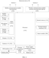
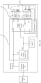
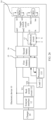
- the system includes an electronic device 10 and a charger 20.
- a battery 14 in the electronic device 10 may be charged by the charger 20 connected externally.
- the charger 20 includes a charger body 21 and a plug 22 connected to the charger body 21 and the electronic device 10 further includes an external interface 12, a load 11, and a power supply system 13.
- the battery 14 includes a plurality of cells. In the embodiment of this application, the plurality of cells in the battery are described in a form of a plurality of cell groups.
- each cell group includes at least one cell, and at least one cell is coupled between two poles (positive+ and negative-) of the cell group.
- the cell group may be one cell.
- a small electronic device such as a mobile phone or a tablet computer
- the voltage of one cell is enough to meet the system rated voltage Vbat of electronic device
- a similar small electronic device usually includes a small number of cells, such as 2-4 cells, and the cells are connected in parallel to supply power to the load. Therefore, connecting a plurality of cells in parallel mainly aims at providing a larger capacity to meet the requirement for prolonging the standby time of the device.
- the system rated voltage Vbat may have one or more high voltages, which may be several times of the voltage of one cell. Therefore, it is necessary to connect a plurality of cells in series in the cell group to reach the system rated voltage Vbat of the device, and then the plurality of cell groups are connected in parallel to supply power to the load. Therefore, the embodiment of this application does not limit the number of cell groups in the battery, the number of cells in the cell group, and the connection mode of the cells in the cell group. It can be understood that when a plurality of cells are included in the cell group, the cells may be connected in parallel or in series.
- the battery 14 is connected to the external interface 12 and the load 11 through the power supply system 13 according to the embodiment of this application.
- the embodiment of this application mainly describes switching of the connection status of the cell groups by the power supply system 13 during switching between a state in which the charger 20 charges the plurality of cell groups and a state in which the plurality of cell groups discharges to the load 11, so as to adapt to charging or discharging of the cell groups.
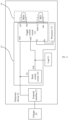
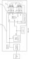
- FIG. 4 shows a schematic structural diagram of an electronic device 100.
- the electronic device 100 may include a processor 110, an external memory interface 120, an internal memory 121, a universal serial bus (universal serial bus, USB) interface 130, a charge management module 140, a power supply management module 141, a battery 142, an antenna 1, an antenna 2, a mobile communications module 150, a wireless communications module 160, an audio module 170, a speaker 170A, a receiver 170B, a microphone 170C, an headphone interface 170D, a sensor module 180, a camera 193, and a display 194, or the like.
- a processor 110 an external memory interface 120, an internal memory 121, a universal serial bus (universal serial bus, USB) interface 130, a charge management module 140, a power supply management module 141, a battery 142, an antenna 1, an antenna 2, a mobile communications module 150, a wireless communications module 160, an audio module 170, a speaker 170A, a receiver 170B, a microphone 170C, an headphone interface 170D, a sensor module 180,
- the schematic structure provided in the embodiments of the present invention does not constitute specific limitation to the electronic device 100.
- the electronic device 100 may include more or fewer components than those shown in the figure, or some components may be combined, or some components may be split, or different component arrangements may be used.
- the components shown in the figure may be implemented by hardware, software, or a combination of software and hardware.
- the processor 110 may include one or more processing units.
- the processor 110 may include an application processor (application processor, AP), a modulation and demodulation processor, a graphics processing unit (graphics processing unit, GPU), an image signal processor (image signal processor, ISP), a controller, a video codec, a digital signal processor (digital signal processor, DSP), a baseband processor, and/or a neural-network processing unit (neural-network processing unit, NPU).
- an application processor application processor, AP
- a modulation and demodulation processor e.g., a graphics processing unit, GPU
- image signal processor image signal processor
- controller e.g., a graphics processing unit
- video codec image signal processor
- DSP digital signal processor
- baseband processor a baseband processor
- NPU neural-network processing unit
- Different processing units may be separate devices, or may be integrated into one or more processors.
- the processor 110 may be further provided with a memory for storing instructions and data.
- the memory in processor 110 is a cache memory.
- the memory may store instructions or data that have just been used or recycled by the processor 110. If the processor 110 needs to reuse the instructions or data, the processor 110 may invoke the instructions or data directly from the memory. Repeated accesses are avoided and waiting time of the processor 110 is reduced thereby improving system efficiency.
- the processor 110 may include one or more interfaces.
- the interfaces may include an inter-integrated circuit (inter-integrated circuit, I2C) interface, an inter-integrated circuit sound (inter-integrated circuit sound, I2S) interface, a pulse code modulation (pulse code modulation, PCM) interface, a universal asynchronous receiver/transmitter (universal asynchronous receiver/transmitter, UART) interface, a mobile industry processor interface (mobile industry processor interface, MIPI), a general-purpose input/output (general-purpose input/output, GPIO) interface, a subscriber identity module (subscriber identity module, SIM) interface, and/or a universal serial bus (universal serial bus, USB) interface.
- I2C inter-integrated circuit
- I2S inter-integrated circuit sound
- PCM pulse code modulation
- PCM pulse code modulation
- UART universal asynchronous receiver/transmitter
- MIPI mobile industry processor interface
- GPIO general-purpose input/output
- SIM subscriber
- the charge management module 140 is configured to receive a charge input from the charger.
- the charger may be a wireless charger or a wired charger.
- the charge management module 140 may receive a charging input from a wired charger through a USB interface 130.
- the charge management module 140 may receive a wireless charging input through a wireless charging coil of the electronic device 100.
- the charge management module 140 may further supply power to the electronic device through the power supply management module 141.
- the power supply management module 141 is configured to connect the battery 142, the charge management module 140, and the processor 110.
- the power supply management module 141 receives an input from the battery 142 and/or the charge management module 140 to supply power to the processor 110, the internal memory 121, the display 194, the camera 193, and the wireless communications module 160.
- the power supply management module 141 may further be configured to monitor parameters such as battery capacity, battery cycle times, battery health status (leakage or impedance), and the like.
- the power supply management module 141 may alternatively be disposed in the processor 110.
- the power supply management module 141 and the charge management module 140 may alternatively be disposed in the same device.
- the wireless communication function of the Electronic Device 100 may be implemented by the antenna 1, the antenna 2, the mobile communications module 150, the wireless communications module 160, the modulation and demodulation processor, and the baseband processor, or the like.
- the antenna 1 and the antenna 2 are configured to transmit and receive electromagnetic wave signals.
- Each antenna in the electronic device 100 may be used to cover a single or a plurality of communication frequency bands. Different antennas may further be multiplexed to improve the utilization rate of the antennas.
- the antenna 1 may be multiplexed to a diversity antenna of a wireless local area network. In other embodiments, the antennas may be used in combination with a tuning switch.
- the mobile communications module 150 may provide a solution including wireless communication such as 2G/3G/4G/5G applied on the electronic device 100.
- the mobile communications module 150 may include one or more filters, switches power amplifiers, low noise amplifiers (low noise amplifier, LNA), and the like.
- the mobile communications module 150 may receive electromagnetic waves by the antenna 1, filter and amplify the received electromagnetic waves, and transmit the electromagnetic waves to the modulation and demodulation processor for demodulation.
- the mobile communications module 150 may alternatively amplify the signal modulated by the modulation and demodulation processor and convert the signal into electromagnetic waves through the antenna 1 to be radiated.
- at least some of the functional modules of the mobile communications module 150 may be disposed in the processor 110.
- at least some of the functional modules of the mobile communications module 150 may be disposed in the same device as at least some of the modules of the processor 110.
- the modulation and demodulation processor may include a modulator and a demodulator.
- the modulator is configured to modulate a low frequency baseband signal to be sent into a medium and high frequency signal.
- the demodulator is configured to demodulate the received electromagnetic wave signal to a low frequency baseband signal. Then the demodulator transmits the demodulated low frequency baseband signal to the baseband processor for processing. After being processed by the baseband processor, the low frequency baseband signal is transmitted to the application processor.
- the application processor outputs a sound signal through an audio device (not limited to the speaker 170A and the receiver 170B or the like) or displays an image or video through the display 194.
- the modulation and demodulation processor may be an independent device.
- the modulation and demodulation processor may be independent of the processor 110 and may be located in the same device as the mobile communications module 150 or other functional modules.
- the wireless communications module 160 may provide a wireless communication solution including a wireless local area network (wireless local area network, WLAN) (such as a wireless fidelity (wireless fidelity, Wi-Fi) network), Bluetooth (Bluetooth, BT), global navigation satellite system (global navigation satellite system, GNSS), frequency modulation (frequency modulation, FM), near field communication (near field communication, NFC), infrared (infrared, IR), and the like, applied to the electronic device 100.
- the wireless communications module 160 may be one or more devices integrating one or more communication processing modules.
- the wireless communications module 160 receives electromagnetic waves via the antenna 2, modulates and filters the electromagnetic wave signal and transmits the processed signal to the processor 110.
- the wireless communications module 160 may alternatively receive a signal to be sent from the processor 110, modulate and amplify the signal, and convert the signal into electromagnetic waves through the antenna 2 to be radiated.
- the antenna 1 of the electronic device 100 is coupled to the mobile communications module 150 and the antenna 2 is coupled to the wireless communications module 160, so that the electronic device 100 may communicate with a network and other devices through the wireless communication technology.
- the wireless communication technologies may include global system for mobile communications (global system for mobile communications, GSM), general packet radio service (general packet radio service, GPRS), code division multiple access (code division multiple access, CDMA), wideband code division multiple access (wideband code division multiple access, WCDMA), time-division code division multiple access (time-division code division multiple access, TD-SCDMA), long term evolution (long term evolution, LTE), BT, GNSS, WLAN, NFC, FM, and/or IR technologies.
- GSM global system for mobile communications
- GPRS general packet radio service
- code division multiple access code division multiple access
- CDMA wideband code division multiple access
- WCDMA wideband code division multiple access
- time-division code division multiple access time-division code division multiple access
- the GNSS may include global positioning system (global positioning system, GPS), global navigation satellite system (global navigation satellite system, GLONASS), beidou navigation satellite system (beidou navigation satellite system, BDS), quasi-zenith satellite system (quasi-zenith satellite system, QZSS) and/or satellite based augmentation systems (satellite based augmentation systems, SBAS).
- global positioning system global positioning system, GPS
- global navigation satellite system global navigation satellite system
- GLONASS global navigation satellite system
- beidou navigation satellite system beidou navigation satellite system
- BDS quasi-zenith satellite system
- QZSS quasi-zenith satellite system
- SBAS satellite based augmentation systems
- the electronic device 100 implements a display function through a GPU, a display 194, an application processor or the like.
- the GPU is a microprocessor for image processing and connects the display 194 and the application processor.
- the GPU is configured to perform mathematical and geometric calculations and to render graphics.
- the processor 110 may include one or more GPUs that execute program instructions to generate or change display information.
- the display 194 is configured to display an image, a video, and the like.
- the display 194 includes a display panel.
- the display panel may adopt a liquid crystal display (liquid crystal display, LCD), organic light-emitting diodes (organic light-emitting diode, OLED), active matrix organic light-emitting diodes (active matrix organic light-emitting diodes, AMOLED) or active-matrix organic light-emitting diodes (active-matrix organic light-emitting diodes, AMOLED), flexible light-emitting diodes (flexible light-emitting diodes, FLED), Minilized, MicroLed, Micro-oLed, quantum dot light-emitting diodes (quantum dot light-emitting diodes, QLED), or the like.
- LCD liquid crystal display
- OLED organic light-emitting diodes
- AMOLED active matrix organic light-emitting diodes
- AMOLED active-matrix organic light
- the electronic device 100 may include one or N displays 194. N is a positive integer greater than 1.
- the electronic device 100 may implement a photographing function through an ISP, a camera 193, a video codec, a GPU, a display 194, an application processor, or the like.
- the ISP is configured to process data fed back by the camera 193. For example, when taking a picture, a shutter is opened, light is transmitted to a camera photosensitive element through a lens, and an optical signal is converted into an electrical signal, which is transmitted to the ISP for processing and converted into an image visible to naked eyes.
- the ISP may further perform algorithm optimization on the noise, brightness, and skin color of the image.
- the ISP may further perform parameter optimization on exposure, color temperature, or a like of the photographing scene.
- the ISP may be disposed in the camera 193.
- the camera 193 is configured to capture a still image or video.
- An optical image of an object is generated through a lens and is projected to a photosensitive element.
- the photosensitive element may be a charge coupled device (charge coupled device, CCD) or a complementary metal-oxide-semiconductor (complementary metal-oxide-semiconductor, CMOS) phototransistor.
- CCD charge coupled device
- CMOS complementary metal-oxide-semiconductor
- the photosensitive element converts the optical signal to an electrical signal, which is then transmitted to the ISP for conversion into a digital image signal.
- the ISP outputs the digital image signal to the DSP for processing.
- the DSP converts the digital image signal into an image signal of a standard RGB or YUV format.
- the electronic device 100 may include one or N cameras 193. N is a positive integer greater than 1.
- the external memory interface 120 may be configured to connect an external memory card such as a Micro SD card, to enable extension of the storage capacity of the electronic device 100.
- the external memory card communicates with the processor 110 through the external memory interface 120 to implement a data storage function. For example, music, video, and other files are saved in the external memory card.
- the internal memory 121 may be configured to store one or more computer programs, and the one or more computer programs include an instruction.
- the processor 110 may run the foregoing instructions stored in the internal memory 121, so that the electronic device 100 performs the method, various functional applications, data processing, and the like provided in some embodiments of this application.
- the internal memory 121 may include a program storage area and a data storage area.
- the stored program area may store an operating system; and the stored program area may further store one or more applications (such as galleries or contacts).
- the storage data area may store data (for example, photos or contacts) created during use of the electronic device 101.
- the internal memory 121 may include a high-speed random access memory and may further include a non-volatile memory such as one or more disk storage devices, flash memory devices, or universal flash storage (universal flash storage, UFS).
- the processor 110 causes the electronic device 100 to perform the methods provided in embodiments of this application, as well as various functional applications and data processing, by executing the instructions stored in the internal memory 121 and/or the instructions stored in the memory disposed in the processor.
- the electronic device 100 may implement an audio function through an audio module 170, a speaker 170A, a receiver 170B, a microphone 170C, an earphone interface 170D, an application processor, or the like, for example, music playing or recording.
- the audio module 170 is configured to convert a digital audio information into an analog audio signal to output and is further configured to convert an analog audio input into a digital audio signal.
- the audio module 170 may further be configured to encode and decode an audio signal.
- the audio module 170 may be disposed in the processor 110 or some of functional modules of the audio module 170 may be disposed in the processor 110.
- the speaker 170A also referred to as a "horn" is configured to convert an audio electrical signal into a sound signal.
- the electronic device 100 may be used to listen to music or listen to a hands-free call through the speaker 170A.
- the receiver 170B also referred to as a "handset" is configured to convert an audio electrical signal into a sound signal.
- the receiver 170B may be brought close to a human ear for listening.
- the microphone 170C also referred to as " MIC " and "mike", is configured to convert a sound signal into an electrical signal.
- a user may make a sound by approaching the microphone 170C through the human mouth and input a voice signal to the microphone 170C.
- the electronic device 100 may be provided with one or more microphones 170C.
- the electronic device 100 may be provided with two microphones 170C which in addition to collecting sound signals may also implement a noise reduction function.
- the electronic device 100 may also be provided with three, four, or more microphones 170C to implement acquisition of sound signals, noise reduction, recognition of sound sources, directional recording functions, and the like.
- the headphone interface 170D is configured to connect a wired headphone.
- the headphone interface 170D may be a USB interface 130, or a 3.5 mm open mobile terminal platform (open mobile terminal platform, OMTP) standard interface, or a cellular telecommunications industry association of the USA (cellular telecommunications industry association of the USA, CTIA) standard interface.
- the sensor module 180 may include a pressure sensor, a gyro sensor, an air pressure sensor, a magnetic sensor, an acceleration sensor, a distance sensor, a proximity light sensor, a fingerprint sensor, a temperature sensor, a touch sensor, an ambient light sensor, a bone conduction sensor, or the like.
- a touch sensor is also referred to as a "touch device”.
- the touch sensor may be disposed on the display 194, and a touch screen, also referred to as a “touch control screen", is formed by the touch sensor and the display 194.
- the touch sensor is configured to detect a touch operation acting on or near the touch sensor.
- the touch sensor may pass a detected touch operation to the application processor to determine a touch event type.
- Visual output related to touch operation may be provided through the display.
- a touch panel provided with a touch sensor array formed by a plurality of touch sensors may be attached to the surface of the display panel in an external form.
- the touch sensor may alternatively be in a position different from that of the display 194.
- the form of the touch sensor is not limited, for example, the touch sensor may be a device such as a capacitor or a piezoresistor.
- the above-mentioned electronic device may further include one or more components such as a key 190, a motor 191, an indicator 192, and a subscriber identification module (subscriber identification module, SIM) card interface 195, which are not limited by the embodiments of this application.
- a key 190 a motor 191, an indicator 192, and a subscriber identification module (subscriber identification module, SIM) card interface 195, which are not limited by the embodiments of this application.
- SIM subscriber identification module
- an embodiment of this application provides a power supply system 13, applicable to an electronic device 10.
- the electronic device 10 includes a battery 14, an external interface 12, and a load 11.
- the battery 14 includes a plurality of cell groups (BG1, BG2,..., BGn), the load 11 may be any one of the electrical devices shown in FIG. 4 , and the external interface 12 may be the USB interface described above.
- the load 11 may be any of the electrical devices shown in FIG. 4 .
- the power supply system 13 includes a toggle switch circuit 131 and a buck switch circuit 132.
- the toggle switch circuit 131 includes a first output end out1, a second output end out2, a plurality of input ends (in1, in2,... inn) and a plurality of control ends I (I1-Ix).
- Two poles (+,-) of the cell group (BG1, BG2,..., BGm) are each coupled to an input end (in1, in2,..., inn) of the toggle switch circuit 131.
- the first output end out1 of the toggle switch circuit 131 is coupled to an input end VI of the buck switch circuit 132
- the second output end out2 of the toggle switch circuit 131 is coupled to an output end VO of the buck switch circuit 132
- the input end VI of the buck switch circuit 132 is coupled to the external interface 12.
- the output end VO of the buck switch circuit 132 is further coupled to the load 11 of the electronic device 10, and the external interface 12 is configured to connect the charger 20.
- the plug 22 of the charger 20 can be inserted into the external interface 12.
- Related functions of the toggle switch circuit 131 may be configured or controlled by the processor 133, for example, the processor 133 sends a control signal to the control ends I (I1-Ix) of the toggle switch circuit 131 for configuration. In this way, as shown in FIG. 5 , the control end I of the toggle switch circuit 131 is coupled to the control end I/O of the processor 133.
- the processor 133 includes a plurality of control ends I/O, and the plurality of control ends I of the toggle switch circuit 131 and the plurality of control ends I/O of the processor 133 may be one-to-one coupled.
- the processor 133 may be the processor 110 provided in FIG. 3 or a separately disposed processor and the control end I/O of the processor 133 may be an interface to the processor 110.
- the processor 133 may also be an electrical device in the load 11.
- the toggle switch circuit 131 is configured to switch the connection status of the at least two cell groups (BG1, BG2,..., BGm) to be serially-connected or parallelly-connected.
- the toggle switch circuit 131 is configured to switch the connection status of the at least two cell groups (BG1, BG2,..., BGm) to be serially-connected, so that the at least two cell groups (BG1, BG2,..., BGm) are connected in series between the first output end out1 of the toggle switch circuit 131 and the grounding end GND
- the buck switch circuit 132 is configured to adjust the voltage of the charger to the system rated voltage Vbat and output the voltage to the output end VO of the buck switch circuit 132.
- the charger 20 may directly charge the cell groups (BG1, BG2,..., BGm) in the serially-connected state, which, as compared with the solution provided in FIG. 1 , can avoid the situation of charging the cell groups (BG1, BG2,..., BGm) that are in a parallelly-connected state by a charger through a buck switch circuit, reduce the loss in the charging process, and avoid the excessive heating of the mobile phone during charging, thereby improving the charging efficiency.
- the voltage of the charger may be adjusted to the system rated voltage Vbat through the buck switch circuit 132 and outputted to the output end VO of the buck switch circuit 132 to supply power to the load, thereby avoiding power failure of the mobile phone in the charging process and ensuring normal operating of the mobile phone in the charging process.
- the toggle switch circuit 131 When supplying power to the load 14 by the at least two cell groups, the toggle switch circuit 131 is configured to switch the connection status of the at least two cell groups (BG1, BG2,..., BGm) to be parallelly-connected, so that the at least two cell groups (BG1, BG2,..., BGm) are connected in parallel between the second output end out2 of the toggle switch circuit 131 and the grounding end GND, to supply power to the load.
- the toggle switch circuit 131 is configured to switch the connection status of the at least two cell groups (BG1, BG2,..., BGm) to be parallelly-connected, so that the at least two cell groups (BG1, BG2,..., BGm) are connected in parallel between the second output end out2 of the toggle switch circuit 131 and the grounding end GND, to supply power to the load.
- the solution may directly enable the cell groups (BG1, BG2,..., BGm) to be connected in parallel to supply power to the load, and the buck switch circuit is no longer used to reduce the voltage of the serially-connected cell groups in the process of supplying power to the load by using the cell group, so that the loss caused by the buck switch circuit to the cell groups in the buck process can be avoided, and standby time of the mobile phone can be improved.
- the cell groups BG1, BG2,..., BGm
- the toggle switch circuit 132 in order to switch the connection status of the cell groups (BG1, BG2,..., BGm), the toggle switch circuit 132 includes a plurality of switches, and a control end of any one of the switches is coupled to an control end I (I1-Ix) of the toggle switch circuit 132.
- the toggle switch circuit 131 is configured to control the status of one or more of the switches to switch the connection status of the at least two cell groups to a serially-connected state or a parallelly-connected state.
- the toggle switch circuit 131 includes five switches (S1-S5) and the battery includes two battery packs, each of which includes one cell. Two cells (B1, B2) are shown in FIG. 6 .
- a first end of the switch S1 is coupled to the second output end out2 of the toggle switch circuit 131, a second end of the switch S1 is coupled to the third input end in3 of the toggle switch circuit 131, and a control end of the switch S1 is coupled to a control end I1 of the toggle switch circuit 131.
- a first end of the switch S2 is coupled to the fourth input end in4 of the toggle switch circuit 131, a second end of the switch S2 is coupled to the second input end in2 of the toggle switch circuit 131, and a control end of the switch S2 is coupled to a control end I2 of the toggle switch circuit 131.
- a first end of the switch S3 is coupled to the second input end in2 of the toggle switch circuit 131, a second end of the switch S3 is coupled to the third input end in3 of the toggle switch circuit 131, and a control end of the switch S3 is coupled to a control end 13 of the toggle switch circuit 131.
- a first end of the switch S4 is coupled to the first output end out1 of the toggle switch circuit 131, a second end of the switch S4 is coupled to the first input end in1 of the toggle switch circuit 131, and a control end of the switch S4 is coupled to a control end I4 of the toggle switch circuit 131.
- a first end of the switch S5 is coupled to the second output end out of the toggle switch circuit 131, a second end of the switch S5 is coupled to the first input end in1 of the toggle switch circuit 131, and a control end of the switch S5 is coupled to a control end 15 of the toggle switch circuit 131.
- a positive pole (+) of the first cell B1 is coupled to the third input end in3 of the toggle switch circuit 131, a negative pole (-) of the first cell B1 is coupled to the fourth input end in4 of the toggle switch circuit 131, a positive pole (+) of the second cell B2 is coupled to the first input end in1 of the toggle switch circuit 131, a negative pole (-) of the second cell B2 is coupled to the second input end in2 of the toggle switch circuit 131, and the fourth input end in4 of the toggle switch circuit 131 is coupled to the grounding end GND.
- S1, S2, and S5 in the toggle switch circuit 131 may be controlled to be turned on, and S3 and S4 in the toggle switch circuit 131 may be controlled to be turned off, so that the connection status of the cells B1 and B2 is switched to be parallelly-connected.
- S1, S2, and S5 in the toggle switch circuit 131 are controlled to be turned off and S3 and S4 in the toggle switch circuit 131 are controlled to be turned on, so that the connection status of the cells B1 and B2 is switched to be parallelly-connected.
- the switches in the toggle switch circuit 131 are mainly switched between two states, i.e., turned on and turned off, under the control of the respective control ends.
- the first end of the switch is short-circuited (conductive) with the second end.
- the first end of the switch is open from the second end.
- the switch may adopt a switch transistor, where the first end of the switch may be a source of the switch transistor and the second end of the switch may be a drain of the switch transistor; or the first end may be the drain of the switch transistor and the second end of the switch may be the source of the switch transistor; and the control end of the switch is a gate of the switch transistor.
- the switch transistor is an N-type transistor, when the gate is at a high level, the switch is turned on, and when the gate is at a low level, the switch is turned off.
- the switch transistor is a P-type transistor
- the switch when the gate is at a low level, the switch is turned on, and when the gate is at a high level, the switch is turned off.
- the switches in the embodiment corresponding to FIG. 6 and in the following embodiments are mainly described with an N-type transistor as an example.
- the processor 133 may control the switch to be turned on by outputting a high-level signal to the gate of the N-type transistor or outputting a low-level signal to the gate of the N-type transistor, to control the switch to be turned off. Referring to FIG.
- the output end VO of the buck switch circuit 132 is further connected to a first capacitor C1, where C1 is connected in series between the output end VO of the buck switch circuit 132 and the grounding end GND, and a voltage-resistance value of C1 is greater than or equal to the system rated voltage Vbat.
- FIG. 7 provides a specific structure of the buck switch circuit 132, including a switch buck chip, capacitors C2, C3, and an inductor L1.
- the switch buck chip is mainly integrated with a switch tube and a controller of the switch tube, where a power supply end Vin of the switch buck chip serves as the input end VI of the buck switch circuit 132, and the output end SW of the switch buck chip is connected to the output end VO of the buck switch circuit 132 through the inductor L1.
- the capacitor C2 is coupled between the power supply end Vin of the switch buck chip and the grounding end GND
- the capacitor C3 is coupled between the output end VO of the buck switch circuit 132 and the grounding end GND
- the output end VO of the buck switch circuit 132 is further coupled to a feedback end RE of the switch buck chip.
- the switch buck chip mainly controls the status of the internal integrated switch tube through the controller to reduce the voltage of the input end VI and output the voltage to the output end VO.
- the voltage outputted from the output end VO may be sampled to implement closed loop processing of buck control. Specifically, as shown in FIG.
- the switch buck chip is mainly integrated with switch tubes k1, k2, and a controller of the switch tubes, where the switch tubes may adopt MOSFET or IGBT.
- the switch tubes may adopt MOSFET or IGBT.
- both k1 and k2 adopt N-type MOSFET, where a source of k1 is connected to the SW, a drain of k1 is connected to Vin, a source of k2 is connected to the grounding end GND, and a drain of k2 is connected to the SW.
- the grids of K1 and K2 are each connected to a controller and the feedback end RE is connected to the controller.
- k2 may alternatively be replaced by a reverse-connected diode D, where an anode of the diode is connected to the grounding end GND and a cathode of the diode D is connected to the SW.
- the buck switch circuit 132 may adopt a buck charge pump.
- FIG. 9 provides a typical 2:1 buck charge pump.
- the buck switch circuit 132 includes a controller, switches k3, k4, k5, k6, and capacitors C4, C5, C6, where a first end of k3 is coupled to the input end VI of the buck switch circuit 132, a second end of k3 is coupled to a first end of k5, and a second end of k5 is coupled to the output end VO of the buck switch circuit 132; C4 is coupled between the input end VI of the buck switch circuit 132 and the grounding end GND; a first end of k4 is coupled to the output end VO of the buck switch circuit 132, a second end of k4 is coupled to a first end of k6, and the second end of k6 is coupled to the grounding end GND; a positive pole of C5 is coupled to a first end of k5 and a negative pole of C5 is coupled to
- the control ends of the switches k3, k4, k5 and k6 are coupled to a controller.
- the controller can generate two timing signals, i.e., a first driving timing signal and a second driving timing signal, with a non-overlapping phases.
- the first driving timing signal and the second driving timing signal being with non-overlapping phases indicates that the first driving timing signal and the second driving timing signal do not simultaneously be at a high level or at a low level.
- the first driving timing signal is outputted to the control ends of k3 and k4, and the second driving timing signal is outputted to the control ends of k5 and k6, so that in the first stage, when the first driving timing signal controls k3 and k4 to be turned on and the second driving timing signal controls k5 and k6 to be turned off, the positive pole of C5 is connected to VI, and the negative pole of C5 is connected to VO.
- C6 is coupled between VO and the grounding end GND, and therefore the voltage inputted to VI charges C5 and C6 connected in series. In this case, part of the current through the capacitor C5 flows through C6 and the other part flows to the load through VO.
- FIG. 9 describes only a typical buck voltage pump, and it can be understood that any buck switch circuit based on the principle is suitable for this application.
- the toggle switch circuit includes eight switches and three cell groups.
- the toggle switch circuit 131 includes eight switches (S1-S8), the battery includes three battery packs, each of which includes one cell. Three cells (B1, B2, B3) are shown in FIG. 10 .
- a first end of the switch S1 is coupled to the second output end out2 of the toggle switch circuit 131, a second end of the switch S1 is coupled to a fifth input end in5 of the toggle switch circuit 131, and a control end of the switch S1 is coupled to a control end I1 of the toggle switch circuit 131.
- a first end of the switch S2 is coupled to a sixth input end in6 of the toggle switch circuit 131, a second end of the switch S2 is coupled to the fourth input end in4 of the toggle switch circuit 131, and a control end of the switch S2 is coupled to a control end I2 of the toggle switch circuit 131.
- a first end of the switch S3 is coupled to the fourth input end in4 of the toggle switch circuit 131, a second end of the switch S3 is coupled to the fifth input end in5 of the toggle switch circuit 131, and a control end of the switch S3 is coupled to a control end I3 of the toggle switch circuit 131.
- a first end of the switch S4 is coupled to the second input end in2 of the toggle switch circuit 131, a second end of the switch S4 is coupled to the third input end in3 of the toggle switch circuit 131, and a control end of the switch S4 is coupled to a control end I4 of the toggle switch circuit 131.
- a first end of the switch S5 is coupled to the second output end out2 of the toggle switch circuit 131, a second end of the switch S5 is coupled to the third input end in3 of the toggle switch circuit 131, and a control end of the switch S5 is coupled to a control end I5 of the toggle switch circuit 131.
- a first end of the switch S6 is coupled to the sixth input end in6 of the toggle switch circuit 131, a second end of the switch S6 is coupled to the second input end in2 of the toggle switch circuit 131, and a control end of the switch S6 is coupled to a control end I6 of the toggle switch circuit 131.
- a first end of the switch S7 is coupled to a second output end out2 of the toggle switch circuit 131, a second end of the switch S7 is coupled to the first input end in1 of the toggle switch circuit 131, and a control end of the switch S7 is coupled to a control end I7 of the toggle switch circuit 131.
- a first end of the switch S8 is coupled to the first output end out1 of the toggle switch circuit 131, a second end of the switch S8 is coupled to the first input end in1 of the toggle switch circuit 131, and a control end of the switch S8 is coupled to a control end I8 of the toggle switch circuit 131.
- a positive pole (+) of the first cell B1 is coupled to the fifth input end in5 of the toggle switch circuit 131, a negative pole (-) of the first cell B1 is coupled to the sixth input end in6 of the toggle switch circuit 131, a positive pole (+) of the second cell B2 is coupled to the third input end in3 of the toggle switch circuit 131, a negative pole (-) of the second cell B2 is coupled to the fourth input end in4 of the toggle switch circuit 131, a positive pole (+) of the third cell B3 is coupled to the first input end in1 of the toggle switch circuit 131, a negative pole (-) of the third cell B3 is coupled to the second input end in2 of the toggle switch circuit 131, and the sixth input end in6 of the toggle switch circuit 131 is coupled to the grounding end GND.
- S1, S2, S5, S6, and S7 in the toggle switch circuit 131 may be controlled to be turned on, and S3, S4, and S8 in the toggle switch circuit 131 may be controlled to be turned off, so that the connection status of the cells B1, B2, and B3 is switched to be parallelly-connected.
- S1, S2, S5, S6, and S7 in the toggle switch circuit 131 are controlled to be turned off and S3, S4, and S8 in the toggle switch circuit 131 are controlled to be turned on, so that the connection status of the cells B1, B2, and B3 is switched to be parallelly-connected.
- the load power-off situation may occur when a plurality of cell groups are switched between serially-connected and parallelly-connected states. For example, in a case that the connection status of the cell groups is serially-connected state and the charger charges the cell groups, if the charger is suddenly pulled out or the cell groups are fully charged and the charger is pulled out, the charger stops supplying power to the buck switch circuit. In this case, the cell groups are connected in series and then supplies power to the buck switch circuit.
- the load power-off situation may occur because there is a response time for switching between turned-on and turned-off states of the switches.
- S1, S2 and S5 are turned off and S3 and S4 are turned on
- the cell groups are in the serially-connected state, and the charger charges the cell group.
- the charger is pulled out, it is necessary to turn on S1, S2, and S5 and turn off S3 and S4.
- the cell groups stop supplying power to the buck switch circuit, no cell group is connected to the load during the period, and therefore the load may be powered off.
- the status of the switches in the toggle switch circuit is triggered and controlled to switch the connection status of the cell groups to be serially-connected for charging, and in this case, the charger supplies power to the load through the buck switch circuit.
- the charger stops supplying power to the buck switch circuit. In this case, if no cell group is connected to the load to supply power to the load, the load may be powered off. As shown in FIG.
- an embodiment of this application further provides a method for switching a connection status of a cell, which can prevent power-off of the load during the process of switching the cell groups between the serially-connected state and the parallelly-connected state.
- Scenario 1 When the cell groups are fully charged, the connection status of the cell groups is triggered to switch from the serially-connected state to the parallelly-connected state.
- the toggle switch circuit 131 is configured to switch the connection status of the at least two cell groups (BG1, BG2,..., BGm) to be serially-connected, so that the at least two cell groups (BG1, BG2,..., BGm) are connected in series between the first output end out1 of the toggle switch circuit 131 and the grounding end GND, and the buck switch circuit 132 is configured to adjust a voltage of the charger 20 to a system rated voltage Vbat and output the voltage to the output end VO of the buck switch circuit 132.
- the charger 20 charges the cell groups (BG1, BG2,..., BGm) connected in series, and the charger 20 supplies power to the load 11 through the buck switch circuit 132. Subsequently, if it is determined that the cell groups (BG1, BG2,..., BGm) are fully charged, switching of the connection status of the cell groups (BG1, BG2,..., BGm) from the serially-connected state to the parallelly-connected state is triggered, specifically including the following steps: S101: When it is determined that charging is completed, control a buck switch circuit 132 to adjust a voltage outputted by an output end VO of the buck switch circuit 132 to a voltage of a first cell group BG1 in at least two cell groups (BG1, BG2,..., BGm).
- the first cell group BG1 may be any cell group.
- a processor 133 may detect a charging current of a first output end out1 of the toggle switch circuit 131 and determine that charging is completed when the charging current remains at a predetermined constant value for a predetermined period of time and does not become small again.
- the charger 20 outputs the voltage of the first cell group BG1 to the load 11 through a buck switch circuit 132 to supply power to the load 11.
- the charger 20 supplies power to the load 11 through the buck switch circuit 132, and the at least two cell groups (BG1, BG2,..., BGm) connected in series prepare power for the load 11 for the load through the buck switch circuit 132, to ensure that the load 11 is continuously powered.
- step S102 the processor 133 controls the toggle switch circuit 131 to output the voltage by the first cell group BG1 to the second output end out2 of the toggle switch circuit 131. Therefore, the first cell group BG1 is connected in parallel with the load 11.
- the voltage outputted by the second output end out2 of the toggle switch circuit 131 is equal to the voltage of the first cell group BG1, and the charger 20 still outputs the voltage of the first cell group BG1 to the load 11 through the buck switch circuit 132 to supply power to the load 11.
- the first cell group BG1 prepares power for the load, and only when the charger 20 is suddenly powered off (for example, pulled out), the first cell group BG1 supplies power to the load 11. In this way, in the process, the load 11 is ensured to be continuously powered.
- S103 Control the toggle switch circuit 131 to switch the connection status of the at least two cell groups (BG1, BG2,..., BGm) to the parallelly-connected state, so that the at least two cell groups (BG1, BG2,..., BGm) are connected in parallel between the second output end out2 of the toggle switch circuit 131 and the grounding end GND.
- step S103 when the connection status of the two cell groups (BG1, BG2,..., BGm) is switched to the parallelly-connected state, only other cell groups (BG2,..., BGm) except the first cell group BG1 need be connected in parallel between the second output end out2 of the toggle switch circuit 131 and the grounding end GND.
- the charger 20 outputs the voltage of the first cell group BG1 to the load 11 through the buck switch circuit 132 to supply power to the load 11, and the first cell group BG1 is connected in parallel with the load to prepare power for the load, to ensure that the load 11 is continuously powered.
- the circuit shown in FIG. 6 and the timing diagrams of the signals at the control ends of the switches shown in FIG. 11 are described in detail in the following (in which the switches are represented by different signs in on and off states):
- the processor 133 controls S1, S2, and S5 in the toggle switch circuit 131 to be turned on and S3 and S4 in the toggle switch circuit 131 to be turned off, to switch the connection status of the cells B1 and B2 to the serially-connected state (referring to FIG. 12 ), so that the cells B1 and B2 are connected in series between the first output end out1 of the toggle switch circuit 131 and the grounding end GND.
- the processor 133 controls the buck switch circuit 132 to adjust the voltage of the charger 20 to the system rated voltage Vbat and output the voltage to the output end VO of the buck switch circuit 132.
- the charger 20 supplies a charging voltage Vbus negotiated with the processor 133 of the electronic device to the input end VI of the buck switch circuit 132.
- the cells B1 and B2 are connected in series, the charging voltage Vbus is at least twice of the system rated voltage Vbat.
- the buck switch circuit 132 is controlled to adjust the voltage outputted by the output end VO of the buck switch circuit 132 to the voltage of the cell B1, for example, Vbat.
- the processor 133 controls S1 to be turned on, and in this case, the cell group B1 is connected to the second output end out2 of the toggle switch circuit 131 to output the voltage to the second output end out2 of the toggle switch circuit 131.
- the voltage outputted by the second output end out2 of the toggle switch circuit 131 is equal to the voltage of the cell B1
- the charger 20 still outputs Vbat to the load 11 through the buck switch circuit 132 to supply power to the load 11, and the cell B1 prepares power for the load.
- the processor 133 controls S3 and S4 to be turned off, so that the cells B1 and B2 are disconnected from the serially-connected circuit.
- S5 and S2 are controlled to be turned on, so that the cells B2 and B1 are connected in parallel.
- the cells B1 and B2 are connected in parallel between the second output end out2 of the toggle switch circuit 131 and the grounding end GND. If the charger 20 is not pulled out, the charger 20 still outputs Vbat to the load 11 through the buck switch circuit 132 to supply power to the load 11. The cells B1 and B2 prepare power for the load. In t5 period of time, the charger 20 is pulled out, and the cells B1 and B2 are connected in parallel to supply power to the load 11.
- Scenario 2 In the process of charging the cell groups by the charger in the serially-connected state, the charger is pulled out to stop charging the cell groups, which triggers the switching of the connection status of the cell groups from the serially-connected state to the parallelly-connected state.
- the toggle switch circuit 131 is configured to switch the connection status of the at least two cell groups (BG1, BG2,..., BGm) to be serially-connected, so that the at least two cell groups (BG1, BG2,..., BGm) are connected in series between the first output end out1 of the toggle switch circuit 131 and the grounding end GND, and the buck switch circuit 132 is configured to adjust a voltage of the charger 20 to a system rated voltage Vbat and output the voltage to the output end VO of the buck switch circuit 132. In this case, the charger charges the cell groups connected in series.
- switching of the connection status of the cell groups from the serially-connected state to the parallelly-connected state is triggered, which specifically includes the following steps: S201: When it is determined that the charger 20 is pulled out, control a buck switch circuit 132 to adjust a voltage outputted by an output end VO of the buck switch circuit 132 to a voltage of a first cell group BG1 in at least two cell groups (BG1, BG2,..., BGm).
- the first cell group BG1 may be any cell group.
- whether the charger 20 is pulled out may be determined by measuring the voltage of the external interface 12.
- the at least two cell groups (BG1, BG2,..., BGm) are connected in series between a first output end out1 of a toggle switch circuit 131 and a grounding end GND. Therefore, the at least two cell groups (BG1, BG2,..., BGm) are connected in series to output a voltage of the first cell group BG1 to a load 11 through the buck switch circuit 132 to supply power to the load 11.
- the at least two cell groups (BG1, BG2,..., BGm) are connected in series to supply power to the load 11 through the buck switch circuit 132, to ensure that the load 11 is continuously powered.
- step S202 the processor 133 controls the toggle switch circuit 131 to output the voltage by the first cell group BG1 to the second output end out2 of the toggle switch circuit 131. Therefore, the first cell group BG1 is connected in parallel with the load 11. Then, in step S202, the voltage outputted by the second output end out2 of the toggle switch circuit 131 is equal to the voltage of the first cell group BG1, and the voltage of the first cell group BG1 is still outputted to the load 11 by the at least two cell groups (BG1, BG2,..., BGm) connected in series through the buck switch circuit 132 to supply power to the load 11. The first cell group BG1 prepares power to the load. In this way, in the process, the load 11 is ensured to be continuously powered.
- S203 Control the toggle switch circuit 131 to switch the connection status of the at least two cell groups (BG1, BG2,..., BGm) to the parallelly-connected state, so that the at least two cell groups (BG1, BG2,..., BGm) are connected in parallel between the second output end out2 of the toggle switch circuit 131 and the grounding end GND.
- step S202 the at least two cell groups (BG1, BG2,..., BGm) are connected in series to output the voltage of the first cell group BG1 to the load 11 through the buck switch circuit 132 to supply power to the load 11, and the first cell group BG1 is connected in parallel with the load as a standby power supply. Therefore, in step S203, when the connection status of the at least two cell groups (BG1, BG2,..., BGm) is switched to be parallelly-connected, only other cell groups (BG2,..., BGm) except the first cell group BG1 need to be connected in parallel between the second output end out2 of the toggle switch circuit 131 and the grounding end GND.
- step S203 in a case that the first cell group BG1 is connected in parallel with the load to supply power to the load, when the series connection of the at least two cell groups (BG1, BG2,..., BGm) is disconnected, the load 11 is ensured to be continuously powered.
- the processor 133 controls S1, S2, and S5 in the toggle switch circuit 131 to be turned on and S3 and S4 in the toggle switch circuit 131 to be turned off, to switch the connection status of the cells B1 and B2 to the serially-connected state (referring to FIG. 12 ), so that the cells B1 and B2 are connected in series between the first output end out1 of the toggle switch circuit 131 and the grounding end GND.
- the processor 133 controls the buck switch circuit 132 to adjust the voltage of the charger 20 to the system rated voltage Vbat and output the voltage to the output end VO of the buck switch circuit 132.
- the charger 20 stops supplying voltage to the input end VI of the buck switch circuit 132 and the charging voltage Vbus becomes 0.
- the cells B1 and B2 are connected in series between the first output end out1 of the toggle switch circuit 131 and the grounding end GND, and therefore at the stage, the processor 133 determines that the charger is pulled out, and controls the buck switch circuit 132 to adjust the voltage outputted by the output end VO of the buck switch circuit 132 to the voltage of the cell B1.
- the cells B1 and B2 are connected in series to output the voltage of the cell B1 to the load 11 through the buck switch circuit 132.
- the voltage may be Vbat.
- the processor 133 controls S1 to be turned on, and in this case, the cell group B1 is connected to the second output end out2 of the toggle switch circuit 131 to output the voltage to the second output end out2 of the toggle switch circuit 131.
- the voltage outputted by the second output end out2 of the toggle switch circuit 131 is equal to the voltage of the cell B1, the cells B1 and B2 connected in series still output Vbat to the load 11 through the buck switch circuit 132 to supply power to the load 11, and the cell B1 prepares power for the load.
- the processor 133 controls S3 and S4 to be turned off, so that the cells B1 and B2 exit the serially-connected state.
- connection status of the cell groups is switched from the parallelly-connected state to the serially-connected state.
- Scenario 3 After the external interface is inserted into the charger, the connection status of the cell groups is triggered to switch from the parallelly-connected state to the serially-connected state.
- the toggle switch circuit 131 when the at least two cell groups (BG1, BG2,..., BGm) supplies power to the load 11, the toggle switch circuit 131 is configured to switch the connection status of the at least two cell groups (BG1, BG2,..., BGm) to be parallelly-connected, so that the at least two cell groups (BG1, BG2,..., BGm) are connected in parallel between the second output end out2 of the toggle switch circuit 131 and the grounding end GND to directly supply power to the load 11.
- a user inserts the charger 20 into the electronic device to charge the electrode device. In this case, the charger 20 charges the cell groups (BG1, BG2,..., BGm) in the serially-connected state.
- the first cell group BG1 may be any cell group.
- the processor 133 detects the voltage of the external interface to identify insertion of the charger 20, for example, based on the voltage of the external interface 12, it may be determined a 5-V charger is inserted into the external interface.
- the at least two cell groups (BG1, BG2,..., BGm) are connected in series in the charging state, so that the charging voltage Vbus is at least twice of the system rated voltage Vbat (2 ⁇ Vbat).
- the processor 133 and the charger 20 may negotiate the charging voltage Vbus and adjust the charging voltage to 2 ⁇ Vbat to implement fast charging of the plurality of cell groups (BG1, BG2,..., BGm) connected in series.
- step 301 after the charging voltage is adjusted to 2 ⁇ Vbat, the buck switch circuit 132 is controlled to adjust the voltage outputted by the output end VO of the buck switch circuit 132 to the voltage of the first cell group BG1. In this way, the charger 20 outputs the voltage of the first cell group BG1 to the load 11 through the buck switch circuit 132 to supply power to the load 11. In the process, the charger 20 supplies power to the load 11 through the buck switch circuit 132, and the at least two cell groups (BG1, BG2,..., BGm) are connected in parallel to prepare power for the load.
- S302 Control the toggle switch circuit 131 to control other cell groups (BG2,..., BGm) of the at least two cell groups (BG1, BG2,..., BGm) except the first cell group BG1 to disconnect from the load 11.
- the first cell group BG1 may be any cell group.
- step S301 when the other cell groups (BG2,..., BGm) are disconnected from the load 11, the first cell group BG1 remains to be connected in parallel with the load 11.
- step S202 the voltage outputted by the second output end out2 of the toggle switch circuit 131 is equal to the voltage of the first cell group BG1, and the charger 20 still outputs the voltage of the first cell group BG1 to the load 11 through the buck switch circuit 132 to supply power to the load 11.
- the first cell group BG1 prepares power for the load, and only when the charger 20 is suddenly powered off, the first cell group BG1 supplies power to the load 11. In this way, in the process, the load 11 is ensured to be continuously powered.
- step 302 may alternatively be performed before step 301.
- the toggle switch circuit 131 is controlled to disconnect the other cell groups (BG2,..., BGm) of the at least two cell groups (BG1, BG2,..., BGm) except the first cell group BG1 to disconnect from the load 11.
- the first cell group BG1 supplies power to the load, and after the charging voltage is adjusted to 2 ⁇ Vbat, and the buck switch circuit 132 is controlled so that the voltage outputted by the output end VO of the buck switch circuit 132 is adjusted to the voltage of the first cell group BG1.
- the first cell group BG1 is the load standby power.
- the voltage outputted by the output end VO of the buck switch circuit 132 is the voltage of the first cell group BG1, and therefore the first cell group BG1 is configured to prepare power for the load. In this way, the load 11 may also be ensured to be continuously powered.
- S303 Control the toggle switch circuit 131 to switch the connection status of the at least two cell groups (BG1, BG2,..., BGm) to the serially-connected state, so that the at least two cell groups (BG1, BG2,..., BGm) are connected in series between the first output end out1 of the toggle switch circuit 131 and the grounding end GND.
- step S303 when the connection status of the at least two cell groups (BG1, BG2,..., BGm) is switched to be serially-connected, the charger 20 continues to output the voltage of the first cell group BG1 to the load 11 through the buck switch circuit 132 to supply power to the load 11.
- the charger 20 directly charges the at least two cell groups (BG1, BG2,..., BGm) connected in series, and the at least two cell groups (BG1, BG2,..., BGm) connected in series reduces the voltage through the buck switch circuit 132 to prepare power for the load, to ensure that the load 11 is continuously powered.
- the cells B1 and B2 connected in parallel supply power to the load 11, and the processor 133 controls S1, S2, and S5 in the toggle switch circuit 131 to be turned on and S3 and S4 to be turned off, so that the connection status of the cells B1 and B2 is switched to be parallelly-connected (referring to FIG. 18 ), so that the cells B1 and B2 are connected in parallel between the second output end out2 of the toggle switch circuit 131 and the grounding end GND.
- the battery is discharged until it is necessary to replenish electric energy, a user inserts the charger 20 into the electronic device to charge the electrode device.
- the output voltage of the charger 20 is 5 V (close to the voltage of a single cell), and the processor may determine, based on the voltage of the external interface, that a 5-V charger is inserted into the external interface.
- the cells B1 and B2 are connected in series in the charging state.
- the processor 133 negotiates with the charger 20 that the charging voltage Vbus is at least twice of the system rated voltage Vbat (2 ⁇ Vbat).
- the processor 133 controls the buck switch circuit 132 to adjust the voltage outputted by the output end VO of the buck switch circuit 132 to the voltage of the cell B1, for example, Vbat.
- the processor 133 controls S2, S3, S4, and S5 in the toggle switch circuit 131 to be turned off and S1 to be turned on (referring to FIG. 19 ), so that B2 is disconnected from the load.
- the voltage outputted by the output end VO of the buck switch circuit 132 is the voltage of B1, and therefore the buck switch circuit 132 supplies power to the load and B1 prepares power for the load.
- the voltage outputted by the output end VO of the buck switch circuit 132 may be adjusted to the voltage of the cell B1 in the period of time t1 (point a in FIG.
- the processor 133 controls S3 and S4 to be turned on, switches the cells B1 and B2 to be serially-connected, the charger starts to charge the cells B1 and B2, and the cells B1 and B2 connected in series reduce the voltage through the buck switch circuit 132 to prepare power for the load.
- the processor 133 controls S1 to be turned off, the cell B1 stops supplying power to the load, and the cells B1 and B2 connected in series reduce the voltage through the buck switch circuit 132 to prepare power for the load.
- the electronic device and the charger may adjust the output voltage of the charger and control the charging current to charge the cells B1 and B2 through a protocol.
- the embodiment of this application further provides an equalization mode for the cell groups during the charging process.
- the power supply system 13 further includes a plurality of equalization circuits 134 (134-1,..., 134-m), two ends of one equalization circuit being respectively coupled to two poles of a cell group. Control ends of the equalization circuits are coupled to the control end of the processor 133.
- the control mode of the equalization circuits (134-1,..., 134-m) is described as follows: when it is determined that the voltage difference between the first cell group BG1 and the second cell group BG2 satisfies the predetermined predetermined condition, the equalization circuit 134-1 corresponding to the first cell group BG1 is controlled to shunt the first cell group BG1.
- the equalization circuit 134-1 when a plurality of cell groups are connected in series, because the properties such as the internal resistance are different, when the plurality of cell groups are connected in series and charged, the voltages of the cell groups may not be equal.
- the equalization circuit (134-1,...,134-m) does not work.
- the voltage difference between the first cell group BG1 and the second cell group BG2 exceeds a first voltage difference threshold, for example, when the voltage of the first cell group BG1 exceeds the voltage of the second cell group BG2 by a value greater than the first voltage difference threshold, it indicates that there is severe imbalance between the plurality of cell groups in the charging process, and a charging current of the first cell group BG1 may be shunted by enabling the equalization circuit 134-1 corresponding to the first cell group BG1, thereby reducing the charging current of BG1 and reducing the charging speed of BG1.
- the control equalization circuit 134-1 is controlled to stop shunting the charging current of the first cell group BG1, where the first voltage difference threshold is greater than the second voltage difference threshold.
- each of the equalization circuits includes a switch and a resistor; a series structure of the switch and the resistor is connected in parallel with a cell group, and a control end of the switch is coupled to a control end of the equalization circuit.
- the equalization circuit 134-1 includes a switch S9 and a resistor R1; the series structure of the switch S9 and the resistor R1 is connected in parallel with the cell group BG1, and a control end of the switch S9 is coupled to the control end of the equalization circuit 134-1.
- the switch S9 in the equalization circuit 134-1 corresponding to the first cell group BG1 may be controlled to be turned on. Specifically, the processor 133 may output a square wave signal to the control end of the switch S9 to control the switch S9 to be intermittently turned on for a period of time. When the processor 133 determines that the voltage difference between the first cell group BG1 and the second cell group BG2 satisfies the second predetermined condition, the switch S9 in the equalization circuit 134-1 corresponding to the first cell group BG1 is turned off.
- an embodiment of this application further provides an equalization circuit 135.
- the equalization circuit 135 includes an equalization switch circuit 1351 and a capacitor C7, a first input end x1 of the equalization switch circuit 135 is coupled to the positive pole of the cell group BG1, a second input end x2 of the equalization switch circuit 135 is coupled to the negative pole of the cell group BG1, a third input end x3 of the equalization switch circuit 135 is coupled to the positive pole of the cell group BG2, and a fourth input end x4 of the equalization switch circuit 135 is coupled to the negative pole of the cell group BG2.
- the capacitor C7 is coupled between the first output end y1 and a second output end y2 of the equalization switch circuit 135.
- the cell group BG1 and the cell group BG2 are adjacent cell groups when the at least two cell groups are connected in series.
- a control end of the equalization switch circuit 135 is coupled to the control end of the processor 133.
- the equalization switch circuit 1351 is controlled to connect the capacitor C7 in parallel with the cell group BG1. In this case, the capacitor C7 shunts a charging current of the cell group BG1, thereby reducing the charging current of the cell group BG1 and reducing the charging speed of the BG1.
- the equalization switch circuit 1351 When it is determined that the voltage of the capacitor C7 is equal to the voltage of the cell group BG1, it indicates that the capacitor C7 is charged to saturation, and the equalization switch circuit 1351 is controlled to connect the capacitor C7 in parallel with the cell group BGm. In this way, the capacitor C7 may charge the cell group BGm.
- the equalization circuit 135 is controlled to stop shunting the charging current of the cell group BG1, where the first voltage difference threshold is greater than the second voltage difference threshold.
- the equalization switch circuit 1351 includes four switches: a switch S10, a switch S11, a switch S12, and a switch S13.
- a first end of the switch S10 is coupled to the first input end x1 of the equalization switch circuit 1351, a second end of the switch S10 is coupled to the first output end y1 of the equalization switch circuit 1351, and a control end of the switch S10 is coupled to a control end of the equalization switch circuit;
- a first end of the switch S11 is coupled to the second input end x2 of the equalization switch circuit 1351, a second end of the switch S11 is coupled to the first output end y1 of the equalization switch circuit 1351, and a control end of the switch S11 is coupled to a control end of the equalization switch circuit 1351;
- a first end of the switch S12 is coupled to the third input end x3 of the equalization switch circuit 1351, a second end of the
- the power supply system further includes a first battery connector 15 and a second battery connector 16.
- the input end VI of the buck switch circuit 132, the output end VO of the buck switch circuit 131, and the control end of the processor 133 are respectively coupled to terminals of the first battery connector 14.
- the first output end out1 of the toggle switch circuit 132, the second output end out2 of the toggle switch circuit 132, and the plurality of control ends (I1-Ix) of the toggle switch circuit 132 are respectively coupled to terminals of the second battery connector 16.
- the first battery connector 15 and the second battery connector 16 are plugged together, the first battery connector 15 is coupled to terminals in the second battery connector 16.
- modularization of a battery can be implemented. For example, when a battery needs to be replaced, the first battery connector 15 and the second battery connector 16 may be directly disconnected to replace the battery.
- a protection circuit 17 is further included.
- the plurality of control ends (I1-Ix) of the toggle switch circuit 131 are each coupled to an output end of the protection circuit 17.
- the protection circuit 17 is configured to sample working parameters of the cell groups, and when it is determined, based on the working parameters, that the working status of any cell group is abnormal, the protection circuit 17 controls the toggle switch circuit 131 to turn off the cell group.
- the protection circuit 17 may sample working parameters such as a current I and a voltage V of the cell group, and control a status of a switch in the toggle switch circuit to disconnect the cell group when it is determined that there are abnormal working states such as undervoltage, overvoltage, and overcurrent short circuit based on the working parameters of the cell group.
- the switches in the toggle switch circuit are directly reused in the abnormal protection process such as undervoltage, overvoltage, and overcurrent short circuit, which can save devices and reduce costs as much as possible.
- the protection circuit 17 may be in the form of a chip.
- the protection circuit 17 may further be coupled to the processor 133, for example, the input end or output end of the protection circuit 17 may be coupled to the control end of the processor 133.
- the protection circuit 17 may be coupled to the processor 133 through the first battery connector 15 and the second battery connector 16 when the protection circuit 17 and the battery are modularly disposed together.
- the processor 133 may send a control signal for switches in the toggle switch circuit 131 to the protection circuit 17, and the protection circuit 17 further controls the status of the switches in the toggle switch circuit 131 based on the control signal.
- the protection circuit 17 may further report the working parameters of the cell groups to the processor 133, so that the processor 133 can perform the above-mentioned equalization control based on the working parameters.
- an apparatus for switching the connection status of a cell which includes a corresponding hardware structure and/or software module for executing various functions.
- a person skilled in the art may be easily aware that, in combination with the units and algorithm operations in the examples described in the embodiments disclosed in this specification, this application may be implemented by hardware or a combination of hardware and computer software. Whether a function is performed by hardware or computer software driving hardware depends on particular applications and design constraint conditions of the technical solutions. A person skilled in the art may use different methods to implement the described functions for each particular application, but it should not be considered that the implementation goes beyond the scope of this application.
- each functional module may be divided corresponding to each function, and two or more functions may alternatively be integrated to one processing module.
- the integrated module may be implemented in a form of hardware, or may be implemented in a form of a software functional module. It should be noted that the division of the modules in the embodiment of this application is schematic and is merely logical function division, and there can be other division modes in actual implementation.
- FIG. 27 shows a schematic structural diagram of an apparatus for switching a connection status of a cell 2700.
- the apparatus for switching a connection status of a cell 2700 may be a chip or a system-on-chip in the mobile phone, or other combined devices and components that can implement the functions of the mobile phone.
- the "module” herein may refer to a particular ASIC, circuit, processor and memory that execute one or more software or firmware programs, integrated logic circuit, and/or other devices that may provide the above-mentioned function.
- the apparatus for switching a connection status of a cell 2700 in FIG. 27 includes a processor 2701 and an interface 2702.
- the processor 2701 is coupled to the interface 2702 and a memory 3, and executes one or more computer programs stored in the memory to cause the control apparatus of the power supply system to execute the above-mentioned method for switching the connection status of a cell.
- the processor 2701 may be coupled to the toggle switch circuit 131, the buck switch circuit 132, the equalization circuit 134, the equalization circuit 135, the first battery connector 15, the protection circuit 17 and the like through an interface 2702.
- the apparatus for switching a connection status of a cell 2700 further includes a memory.
- the memory is configured to store necessary program instructions and data, and the processor may 2700 invoke program code stored in the memory to instruct the apparatus for switching a connection status of a cell 2700 to perform the method in any of the above method embodiments.
- the memory may not be in the apparatus for switching a connection status of a cell 2700.
- the apparatus for switching a connection status of a cell 2700 is a chip system
- the apparatus may be composed of a chip or may include a chip and other discrete devices which are not specifically limited in the embodiments of this application.
- FIG. 28 shows a schematic diagram of the composition of a chip system 2800.
- the chip system 2800 may include a processor 2801 and a communications interface 2802 for supporting related devices to implement the functions described in the above-mentioned embodiments.
- the chip system further includes a memory configured to store program instructions and data necessary for the electronic device.
- the chip system may be composed of a chip or may include a chip and other discrete devices.
- the communications interface 2802 may alternatively be referred to as an interface circuit.
- All or some of the functions, or actions, or operations, or steps in the foregoing embodiments may be implemented by using software, hardware, firmware, or any combination thereof.
- the embodiments may be implemented completely or partially in a form of a computer program product.
- the computer program product includes one or more computer instructions or program code.
- the computer instructions or program code When the computer instructions or program code are loaded and executed on a computer, the procedure or functions according to the embodiments of this application are all or partially generated.
- the computer may be a general-purpose computer, a dedicated computer, a computer network, or other programmable apparatuses.
- the computer instructions or program code may be stored in a computer-readable storage medium or may be transmitted from a computer-readable storage medium to another computer-readable storage medium.
- the computer instructions may be transmitted from a website, computer, server, or data center to another website, computer, server, or data center in a wired (for example, a coaxial cable, an optical fiber, or a digital subscriber line (digital subscriber line, DSL)) or wireless (for example, infrared, radio, or microwave) manner.
- the computer-readable storage medium may be any usable medium accessible to a computer, or a data storage device, such as a server or a data center, integrating one or more usable media.
- the usable medium may be a magnetic medium (for example, a floppy disk, a hard disk, or a magnetic tape), an optical medium (for example, a DVD), a semiconductor medium (for example, a solid state disk (solid state disk, SSD)), or the like.
- a magnetic medium for example, a floppy disk, a hard disk, or a magnetic tape
- an optical medium for example, a DVD
- a semiconductor medium for example, a solid state disk (solid state disk, SSD)
Description
- Embodiments of this application relates to the field of power supplies, and in particular, to a power supply system, and an electronic device.
- At present, the emergence of various electronic products, such as mobile phones, tablets, smart wearable devices, electric tools, and electric automobiles, constantly provides convenience for our lives. Accompanied with the rapid development of the electronic products, portable power supply and mobility have increasingly become the development trend.
- For rechargeable electronic products, users' demand for fast charging and long standby is becoming more and more intense. Taking the mobile phones as an example, buck switch circuits are used in all power supply systems of the mobile phones. As shown in
FIG. 1 and FIG. 2 , the schematic structural diagrams of the current two power supply systems are provided.FIG. 1 provides a buck charging solution, generally, a system rated voltage Vbat of a mobile phone does not exceed 6 V, and a plurality of cells in a mobile phone battery (the voltage of a single cell is 3-4 V) are connected in parallel to directly supply power to a load. The voltage outputted from the charger to an external interface of the mobile phone (for example, a USB interface) is 2-4 times of the voltage of the cell. Therefore, it is necessary to reduce the voltage of the charger by a buck switch circuit to charge the cells connected in parallel.FIG. 2 provides a buck power supply solution. In the solution, a plurality of cells (the voltage of a single cell is 3-4 V) in a mobile phone battery are connected in series. In this state, for example, the voltage of two cells connected in series may reach up to 6-8 V, and the voltage outputted from the charger to an external interface of the mobile phone (for example, a USB interface) may be used to directly charge the serially-connected cells. However, because the voltage of the serially-connected cells is higher than the system rated voltage Vbat of the mobile phone, it is necessary to connect a buck switch circuit between the serially-connected cells and a load and reduce the voltage of the serially-connected cells before inputting the voltage to the load. - In the buck charging solution, the loss caused by the buck switch circuit may lead to excessive heating of the mobile phone during charging and affect the charging efficiency of the mobile phone; and in the buck power supply solution, part of the capacity of the cells may be lost in the form of heat consumption during the buck process of the buck switch circuit, which leads to shorter standby time of the mobile phone.
-
KR-A-20200117817 -
WO-A1-2020/199833 describes a charging and discharging circuit for a mobile terminal using a multi-cell battery, the circuit is configured to switch each battery cell in the multi-cell battery to a serial state and connect it to the battery connector when the multi-cell battery is charging; when the multi-cell battery is not charging, switching each battery cell in the multi-cell battery to a parallel state and connecting it to the battery connector. - According to the invention there is provided a power supply system according to
claim 1. Embodiments of the invention are defined in the dependent claims. An example in this application but not part of the invention provides a method for switching a connection status of a cell, a power supply system, and an electronic device, which can switch the connection status of a cell group to be serially-connected when charging the cell group, and switch the connection status of the cell group to be parallelly-connected when the cell group supplies power to a load, so as to improve charging efficiency and reduce heat loss when the cell group supplies power. A first aspect of this disclosure provides a power supply system, applicable to an electronic device. The electronic device includes at least two cell groups, an external interface, and a load, where each of the cell groups includes at least one cell, and the at least one cell is coupled between two poles of the cell group. The power supply system includes a toggle switch circuit and a buck switch circuit. The toggle switch circuit includes a first output end, a second output end, and a plurality of input ends. Two poles of the cell group are each coupled to an input end of the toggle switch circuit. The first output end of the toggle switch circuit is coupled to an input end of the buck switch circuit, the second output end of the toggle switch circuit is coupled to an output end of the buck switch circuit, and the input end of the buck switch circuit is coupled to an external interface. The output end of the buck switch circuit is further coupled to the load, and the external interface is configured to connect a charger. The toggle switch circuit is configured to switch a connection status of at least two cell groups to be serially-connected or parallelly-connected. When the external interface is inserted into the charger to charge the at least two cell groups, the toggle switch circuit is configured to switch the connection status of the at least two cell groups to be serially-connected, so that the at least two cell groups are connected in series between the first output end of the toggle switch circuit and a grounding end, and the buck switch circuit is configured to adjust a voltage of the charger to a system rated voltage and output the voltage to the output end of the buck switch circuit. When supplying power to the load by the at least two cell groups, the toggle switch circuit is configured to switch the connection status of the at least two cell groups to be parallelly-connected, so that the at least two cell groups are connected in parallel between the second output end of the toggle switch circuit and the grounding end. In this way, the toggle switch circuit can switch the connection status of the at least two cell groups to be serially-connected or parallelly-connected. When the external interface is inserted into the charger to charge the at least two cell groups, the buck switch circuit is configured to adjust a voltage outputted by the output end of the buck switch circuit to a voltage of the first cell group; the toggle switch circuit is configured to disconnect other cell groups of the at least two cells except the first cell group from the load; and the toggle switch circuit is configured to switch the connection status of the at least two cell groups to a serially-connected state, wherein the at least two cell groups is connected in series between the first output end of the toggle switch circuit and the grounding end. In this way, the charger may directly charge the cell groups in a serially-connected state, which can avoid the situation of charging the cell groups that are in a parallelly-connected state by a charger through a buck switch circuit at present, reduce the loss in the charging process, and avoid the excessive heating of the mobile phone during charging, thereby improving the charging efficiency. In addition, in the charging process of the mobile phone, the voltage of the charger may be adjusted to the system rated voltage through the buck switch circuit and outputted to the output end of the buck switch circuit to supply power to the load, thereby avoiding power failure of the mobile phone in the charging process and ensuring normal operating of the mobile phone in the charging process. When charging is completed or the charger is disconnected from the external interface, the buck switch circuit is configured to adjust the voltage outputted from the output end of the buck switch circuit to a voltage of a first cell group among the at least two cell groups; the toggle switch circuit is configured such that the first cell group outputs a voltage to the second output end of the toggle switch circuit; the toggle switch circuit is further configured to switch the connection status of the at least two cell groups to be parallelly-connected, so that the at least two cell groups are connected in parallel between the second output end of the toggle switch circuit and the grounding end. Compared with the current solution of buck power supplying the serially-connected cell group through the buck switch circuit, the solution may directly enable the cell groups to be connected in parallel to supply power to the load, and the buck switch circuit is no longer used to reduce the voltage of the serially-connected cell groups in the process of supplying power to the load by using the cell group, so that the loss caused by the buck switch circuit to the cell groups in the buck process can be avoided, and standby time of the electronic device can be improved. - In a possible implementation, the toggle switch circuit includes a plurality of switches, and a control end of any one of the switches is coupled to a control end of the toggle switch circuit. The toggle switch circuit is specifically configured to control the status of one or more of the switches to switch the connection status of the at least two cell groups to be parallelly-connected, or the toggle switch circuit is specifically configured to control the status of one or more of the switches to switch the connection status of the at least two cell groups to be serially-connected.
- In a possible implementation, the power supply system includes two cell groups; the toggle switch circuit includes a first switch, a second switch, a third switch, a fourth switch, and a fifth switch; a first end of the first switch is coupled to the second output end of the toggle switch circuit, a second end of the first switch is coupled to a third input end of the toggle switch circuit, and a control end of the first switch is coupled to a control end of the toggle switch circuit; a first end of the second switch is coupled to a fourth input end of the toggle switch circuit, a second end of the second switch is coupled to a second input end of the toggle switch circuit, and a control end of the second switch is coupled to a control end of the toggle switch circuit; a first end of the third switch is coupled to the second input end of the toggle switch circuit, a second end of the third switch is coupled to the third input end of the toggle switch circuit, and a control end of the third switch is coupled to a control end of the toggle switch circuit; a first end of the fourth switch is coupled to the first output end of the toggle switch circuit, a second end of the fourth switch is coupled to the first input end of the toggle switch circuit, and a control end of the fourth switch is coupled to a control end of the toggle switch circuit; a first end of the fifth switch is coupled to the second output end of the toggle switch circuit, a second end of the fifth switch is coupled to the first input end of the toggle switch circuit, and a control end of the fifth switch is coupled to a control end of the toggle switch circuit; where a positive pole of the first cell group is coupled to the third input end of the toggle switch circuit, a negative pole of the first cell group is coupled to the fourth input end of the toggle switch circuit, a positive pole of the second cell group is coupled to the first input end of the toggle switch circuit, a negative pole of the second cell group is coupled to the second input end of the toggle switch circuit, and the fourth input end of the toggle switch circuit is coupled to the grounding end. The third switch and the fourth switch are turned off, the first switch, the second switch, and the fifth switch are turned on, and the connection status of the at least two cell groups is switched to be parallelly-connected. Alternatively, the third switch and the fourth switch are turned on, the first switch, the second switch, and the fifth switch are turned off, and the connection status of the at least two cell groups is switched to be serially-connected.
- A second aspect of this disclosure provides a power supply system, applicable to an electronic device, where the electronic device includes at least two cell groups, an external interface, and a load, each of the cell groups includes at least one cell, and the at least one cell is coupled between two poles of the cell group; and the power supply system includes a toggle switch circuit and a buck switch circuit. The toggle switch circuit includes a first output end, a second output end, and a plurality of input ends; the two poles of the cell group are each coupled to an input end of the toggle switch circuit; the first output end of the toggle switch circuit is coupled to an input end of the buck switch circuit, the second output end of the toggle switch circuit is coupled to an output end of the buck switch circuit, and the input end of the buck switch circuit is coupled to an external interface; the output end of the buck switch circuit is further coupled to a load, and the external interface is configured to connect a charger; where the toggle switch circuit is configured to switch a connection status of the at least two cell groups to be serially-connected or parallelly-connected; when the external interface is inserted into the charger to charge the at least two cell groups, the toggle switch circuit is configured to switch the connection status of the at least two cell groups to be serially-connected, so that the at least two cell groups are connected in series between the first output end of the toggle switch circuit and a grounding end, and the buck switch circuit is configured to adjust a voltage of the charger to a system rated voltage and output the voltage to the output end of the buck switch circuit. When it is determined that charging is completed or the charger is disconnected from the external interface, the buck switch circuit is configured to adjust the voltage outputted from the output end of the buck switch circuit to a voltage of a first cell group among the at least two cell groups; the toggle switch circuit is configured such that the first cell group outputs a voltage to the second output end of the toggle switch circuit; the toggle switch circuit is configured to switch the connection status of the at least two cell groups to be parallelly-connected, so that the at least two cell groups are connected in parallel between the second output end of the toggle switch circuit and the grounding end.
- When switching the connection status of the at least two cell groups from serially-connected to parallelly-connected, if the switching of the connection status is triggered due to completion of charging, the buck switch circuit is configured to adjust the voltage outputted from the output end of the buck switch circuit to the voltage of the first cell group of the at least two cell groups when it is determined that the charging is completed. In the process, the charger supplies power to the load through the buck switch circuit, and the at least two cell groups connected in series prepare power for the load through the buck switch circuit, to ensure that the load is continuously powered. Then, the toggle switch circuit is configured such that the first cell group output a voltage to the second output end of the toggle switch circuit. The charger still outputs the voltage of the first cell group to the load through the buck switch circuit to supply power to the load, the first cell group prepares power for the load, and the first cell group supplies power to the load only when the charger is suddenly powered off (for example, pulled out). In this way, in the process, the load is ensured to be continuously powered. Finally, the toggle switch circuit is configured to switch the connection status of the at least two cell groups to be parallelly-connected, so that the at least two cell groups are connected in parallel between the second output end of the toggle switch circuit and the grounding end. The charger outputs the voltage of the first cell group to the load through the buck switch circuit to supply power to the load, and the first cell group is connected in parallel with the load to prepare power for the load, to ensure that the load is continuously powered. At any stage in the above process, there is a standby power solution for the load, and therefore the load may not be powered off when the charger is pulled out at any time. It is ensured that the electronic device may not be powered off during the process of switching the connection status of the at least two cell groups from serially-connected to parallelly-connected. In a case that switching of the connection status is triggered by disconnection of the charger from the external interface, when it is determined that the charger is disconnected from the external interface, the buck switch circuit is configured to adjust the voltage outputted from the output end of the buck switch circuit to the voltage of the first cell group of the at least two cell groups. In the process, the at least two cell groups connected in series supply power to the load through the buck switch circuit, to ensure that the load is continuously powered. Then, the toggle switch circuit is configured such that the first cell group output a voltage to the second output end of the toggle switch circuit. Power is still supplied to the load by outputting the voltage of the first cell group by the at least two cell groups connected in series to the load through the buck switch circuit, and the first cell group prepares power for the load. In this way, in the process, the load is ensured to be continuously powered. Finally, the toggle switch circuit is configured to switch the connection status of the at least two cell groups to be parallelly-connected, so that the at least two cell groups are connected in parallel between the second output end of the toggle switch circuit and the grounding end. The first cell group and the load are connected in parallel as the load, to ensure that the load is continuously powered when the at least two cell groups connected in series are disconnected. The load may not be powered off during the above process. It is ensured that the electronic device may not be powered off during the process of switching the connection status of the at least two cell groups from serially-connected to parallelly-connected.
- In a possible implementation, the toggle switch circuit includes a plurality of switches, and a control end of any one of the switches is coupled to a control end of the toggle switch circuit. The toggle switch circuit is controlled to be specifically configured to control a status of one or more of the switches such that the first cell group outputs a voltage of to the second output end of the toggle switch circuit. The toggle switch circuit is specifically configured to control the status of one or more of the switches to switch the connection status of the at least two cell groups to be parallelly-connected.
- In a possible implementation, the power supply system includes two cell groups; the toggle switch circuit includes a first switch, a second switch, a third switch, a fourth switch, and a fifth switch; a first end of the first switch is coupled to the second output end of the toggle switch circuit, a second end of the first switch is coupled to a third input end of the toggle switch circuit, and a control end of the first switch is coupled to a control end of the toggle switch circuit; a first end of the second switch is coupled to a fourth input end of the toggle switch circuit, a second end of the second switch is coupled to a second input end of the toggle switch circuit, and a control end of the second switch is coupled to a control end of the toggle switch circuit; a first end of the third switch is coupled to the second input end of the toggle switch circuit, a second end of the third switch is coupled to the third input end of the toggle switch circuit, and a control end of the third switch is coupled to a control end of the toggle switch circuit; a first end of the fourth switch is coupled to the first output end of the toggle switch circuit, a second end of the fourth switch is coupled to the first input end of the toggle switch circuit, and a control end of the fourth switch is coupled to a control end of the toggle switch circuit; a first end of the fifth switch is coupled to the second output end of the toggle switch circuit, a second end of the fifth switch is coupled to the first input end of the toggle switch circuit, and a control end of the fifth switch is coupled to a control end of the toggle switch circuit; where a positive pole of the first cell group is coupled to the third input end of the toggle switch circuit, a negative pole of the first cell group is coupled to the fourth input end of the toggle switch circuit, a positive pole of the second cell group is coupled to the first input end of the toggle switch circuit, a negative pole of the second cell group is coupled to the second input end of the toggle switch circuit, and the fourth input end of the toggle switch circuit is coupled to the grounding end; when the external interface is inserted into the charger to charge the at least two cell groups, the third switch and the fourth switch are turned on, and the first switch, the second switch, and the fifth switch are turned off; the second switch and the fifth switch are turned off, the first switch, the third switch, and the fourth switch are controlled to be turned on, and the first cell group outputs the voltage to the second output end of the toggle switch circuit; and the third switch and the fourth switch are turned off, and the first switch, the second switch, and the fifth switch are turned on, to switch the connection status of the at least two cell groups to be parallelly-connected.
- In a possible implementation, the power supply system further includes: a plurality of equalization circuits, two ends of one equalization circuit are each coupled to two poles of a cell group. When it is determined that the voltage difference between the first cell group and the second cell group satisfies a predetermined predetermined condition, an equalization circuit corresponding to the first cell group is configured to shunt the first cell group.
- In a possible implementation, the equalization circuit includes a sixth switch and a first resistor. A series structure of the sixth switch and the first resistor is connected in parallel with a cell group. When it is determined that the voltage difference between the first cell group and the second cell group satisfies a first predetermined condition, a sixth switch in the equalization circuit corresponding to the first cell group is turned on.
- In a possible implementation, the power supply system further includes an equalization circuit, where the equalization circuit includes an equalization switch circuit and a capacitor, a first input end of the equalization switch circuit is coupled to the positive pole of the first cell group, a second input end of the equalization switch circuit is coupled to the negative pole of the first cell group, a third input end of the equalization switch circuit is coupled to the positive pole of the second cell group, and a fourth input end of the equalization switch circuit is coupled to the negative pole of the second cell group; the capacitor is coupled between the first output end and the second output end of the equalization switch circuit; the first cell group and the second cell group are adjacent cell groups when the at least two cell groups are connected in series; when it is determined that the voltage difference between the first cell group and the second cell group satisfies the first predetermined condition, the equalization switch circuit is configured to connect the capacitor in parallel with the first cell group; and when it is determined that the voltage of the capacitor is equal to the voltage of the first cell group, the equalization switch circuit is configured to connect the capacitor in parallel with the second cell group.
- In a possible implementation, the equalization switch circuit includes a sixth switch, a seventh switch, an eighth switch, and a ninth switch; a first end of the sixth switch is coupled to the first input end of the equalization switch circuit, a second end of the sixth switch is coupled to the first output end of the equalization switch circuit, and a control end of the sixth switch is coupled to a control end of the equalization switch circuit; a first end of the seventh switch is coupled to the second input end of the equalization switch circuit, a second end of the seventh switch is coupled to the first output end of the equalization switch circuit, and a control end of the seventh switch is coupled to a control end of the equalization switch circuit; a first end of the eighth switch is coupled to the third input end of the equalization switch circuit, a second end of the eighth switch is coupled to the second output end of the equalization switch circuit, and a control end of the eighth switch is coupled to a control end of the equalization switch circuit; a first end of the ninth switch is coupled to the fourth input end of the equalization switch circuit, a second end of the ninth switch is coupled to the second output end of the equalization switch circuit, and a control end of the eighth switch is coupled to a control end of the equalization switch circuit; when it is determined that the voltage difference between the first cell group and the second cell group satisfies the first predetermined predetermined condition, the sixth switch and the eighth switch are turned on, and the seventh switch and the ninth switch are turned off; and when it is determined that the voltage of the capacitor is equal to the voltage of the first cell group, the sixth switch and the eighth switch are turned off, and the seventh switch and the ninth switch are turned on.
- In a possible implementation, the power supply system further includes a first battery connector and a second battery connector, where the input end of the buck switch circuit and the output end of the buck switch circuit are respectively coupled to terminals of the first battery connector; the first output end of the toggle switch circuit and the second output end of the toggle switch circuit are respectively coupled to the terminals of the first battery connector; and when the first battery connector and the second battery connector are plugged together, the first battery connector is coupled to terminals in the second battery connector.
- In a possible implementation, the power supply system further includes a protection circuit, where a control end of the toggle switch circuit is coupled to an output end of the protection circuit; and protection circuit is configured to sample a working parameter of the cell group, and when a working status of any one of the cell groups is determined to be abnormal based on the working parameter, the protection circuit controls the toggle switch circuit to disconnect any one of the cell groups.
- A third aspect provides a power supply system, applicable to an electronic device. The electronic device includes at least two cell groups, an external interface, and a load, where each of the cell groups includes at least one cell, and the at least one cell is coupled between two poles of the cell group. The power supply system includes a toggle switch circuit and a buck switch circuit. The toggle switch circuit includes a first output end, a second output end, and a plurality of input ends. Two poles of the cell group are each coupled to an input end of the toggle switch circuit. The first output end of the toggle switch circuit is coupled to an input end of the buck switch circuit, the second output end of the toggle switch circuit is coupled to an output end of the buck switch circuit, and the input end of the buck switch circuit is coupled to an external interface. The output end of the buck switch circuit is further coupled to the load of the electronic device, and the external interface is configured to connect a charger. The toggle switch circuit is configured to switch the connection status of the at least two cell groups to be serially-connected or parallelly-connected. When supplying power to the load by the at least two cell groups, the toggle switch circuit is configured to switch the connection status of the at least two cell groups to be parallelly-connected, so that the at least two cell groups are connected in parallel between the second output end of the toggle switch circuit and the grounding end. When it is determined that the external interface is connected to the charger, the buck switch circuit is configured to adjust the voltage outputted from the output end of the buck switch circuit to the voltage of the first cell group. The toggle switch circuit is configured to disconnect a cell group of the at least two cells except the first cell group from the load. The toggle switch circuit is configured to switch the connection status of at least two cell groups to the serially-connected state, so that the at least two cell groups are connected in series between the first output end of the toggle switch circuit and the grounding end.
- In an aspect of this disclosure, in the process of switching the connection status of at least two electric cell groups from the parallelly-connected state to the serially-connected state, because switching of the connection status is mainly triggered by connection of the external interface to the charger, when it is determined that the external interface is connected to the charger, the buck switch circuit is configured to adjust the voltage outputted by the output end of the buck switch circuit to the voltage of the first cell group. In the process, the charger outputs the voltage of the first cell group to the load through the buck switch circuit to supply power to the load, and the at least two cell groups are connected in parallel to prepare power for the load. Then, the toggle switch circuit is configured to disconnect other cell groups of the at least two cells except the first cell group from the load. In the process, the charger outputs the voltage of the first cell group to the load through the buck switch circuit to supply power to the load, and the first cell group prepares power for the load, in which way the load is also ensured to be continuously powered. Finally, the toggle switch circuit is configured to switch the connection status of the at least two cell groups to be serially-connected, so that the at least two cell groups are connected in series between the first output end of the toggle switch circuit and the grounding end. In the process, the charger continuously supplies power to the load by outputting the voltage of the first cell group to the load through the buck switch circuit. In addition, the charger directly charges the at least two cell groups connected in series, and the at least two cell groups connected in series prepare power for the load through bucking by the buck switch circuit, to ensure that the load is continuously powered. The load may not be powered off during the above process. It is ensured that the electronic device may not be powered off during the process of switching the connection status of the at least two cell groups from the parallelly-connected state to the serially-connected state.
- In a possible implementation, the toggle switch circuit includes a plurality of switches, and a control end of any one of the switches is coupled to a control end of the toggle switch circuit. The toggle switch circuit is specifically configured to control the status of one or more of the switches, to disconnect other cell groups of the at least two cells except the first cell group from the load. The toggle switch circuit is controlled to be specifically configured to control the status of one or more of the switches to switch the connection status of the at least two cell groups to be serially-connected.
- In a possible implementation, the power supply system includes two cell groups; the toggle switch circuit includes a first switch, a second switch, a third switch, a fourth switch, and a fifth switch; a first end of the first switch is coupled to the second output end of the toggle switch circuit, a second end of the first switch is coupled to a third input end of the toggle switch circuit, and a control end of the first switch is coupled to a control end of the toggle switch circuit; a first end of the second switch is coupled to a fourth input end of the toggle switch circuit, a second end of the second switch is coupled to a second input end of the toggle switch circuit, and a control end of the second switch is coupled to a control end of the toggle switch circuit; a first end of the third switch is coupled to the second input end of the toggle switch circuit, a second end of the third switch is coupled to the third input end of the toggle switch circuit, and a control end of the third switch is coupled to a control end of the toggle switch circuit; a first end of the fourth switch is coupled to the first output end of the toggle switch circuit, a second end of the fourth switch is coupled to the first input end of the toggle switch circuit, and a control end of the fourth switch is coupled to a control end of the toggle switch circuit; a first end of the fifth switch is coupled to the second output end of the toggle switch circuit, a second end of the fifth switch is coupled to the first input end of the toggle switch circuit, and a control end of the fifth switch is coupled to a control end of the toggle switch circuit; where a positive pole of the first cell group is coupled to the third input end of the toggle switch circuit, a negative pole of the first cell group is coupled to the fourth input end of the toggle switch circuit, a positive pole of the second cell group is coupled to the first input end of the toggle switch circuit, a negative pole of the second cell group is coupled to the second input end of the toggle switch circuit, and the fourth input end of the toggle switch circuit is coupled to the grounding end; when the at least two cell groups supply power to the load, the third switch and the fourth switch are turned off, and the first switch, the second switch, and the fifth switch are turned on; the first switch is turned on, the second switch, the third switch, the fourth switch, and the fifth switch are turned off, and other cell groups of the at least two cell groups except the first cell group are disconnected from the load; and the third switch and the fourth switch are turned on, and the first switch, the second switch, and the fifth switch are turned off, so that the connection status of the at least two cell groups is switched to be serially-connected.
- In a possible implementation, the power supply system further includes: a plurality of equalization circuits, two ends of one equalization circuit are each coupled to two poles of a cell group. When it is determined that the voltage difference between the first cell group and the second cell group satisfies a predetermined predetermined condition, an equalization circuit corresponding to the first cell group is configured to shunt the first cell group. Because properties such as internal resistance of all the cell groups are not completely consistent, unbalanced power may occur in the cell groups after charge and discharge cycles in a long run. When a plurality of cell groups are connected in series, because the properties such as the internal resistance are different, when the plurality of cell groups are connected in series and charged, the voltages of the cell groups may not be equal. In a general state, when a charger charges a plurality of cell groups connected in series, the equalization circuit does not work. When it is determined that the voltage difference between the first cell group and the second cell group exceeds a first voltage difference threshold, for example, when the voltage of the first cell group exceeds the voltage of the second cell group by a value greater than the first voltage difference threshold, it indicates that there is severe imbalance between the plurality of cell groups in the charging process, and a charging current of the first cell group may be shunted by enabling the equalization circuit corresponding to the first cell group, thereby reducing the charging current and reducing the charging speed. When the voltage difference between the first cell group and the second cell group is less than a second voltage difference threshold, in particular, the voltage of the first cell group is less than the voltage of the second cell group, the voltage difference is less than the second voltage difference threshold, or the voltage of the second cell group is less than the voltage of the first cell group, and the voltage difference is less than the second voltage difference threshold, the equalization circuit is controlled to stop shunting the charging current of the first cell group, where the first voltage difference threshold is greater than the second voltage difference threshold.
- In a possible implementation, the equalization circuit includes a sixth switch and a first resistor. A series structure of the sixth switch and the first resistor is connected in parallel with a cell group, and a control end of the sixth switch is coupled to the control end of the equalization circuit. When it is determined that the voltage difference between the first cell group and the second cell group satisfies a first predetermined condition, a sixth switch in the equalization circuit corresponding to the first cell group is turned on. In the solution, shunting of the first cell group by the equalization circuit is implemented by controlling the status of the sixth switch.
- In a possible implementation, the power supply system further includes an equalization circuit, where the equalization circuit includes an equalization switch circuit and a capacitor, a first input end of the equalization switch circuit is coupled to the positive pole of the first cell group, a second input end of the equalization switch circuit is coupled to the negative pole of the first cell group, a third input end of the equalization switch circuit is coupled to the positive pole of the second cell group, and a fourth input end of the equalization switch circuit is coupled to the negative pole of the second cell group; the capacitor is coupled between the first output end and the second output end of the equalization switch circuit; and the first cell group and the second cell group are adjacent cell groups when the at least two cell groups are connected in series. When it is determined that the voltage difference between the first cell group and the second cell group satisfies a first predetermined condition, for example, when the voltage of the first cell group exceeds the voltage of the second cell group by a value greater than the first voltage difference threshold, it indicates that there is severe imbalance between the plurality of cell groups in the charging process, the equalization switch circuit connects the capacitor in parallel with the first cell group. In this case, the capacitor shunts a charging current of the first cell group, thereby reducing the charging current of the first cell group and reducing the charging speed of the first cell group. When it is determined that the voltage of the capacitor is equal to the voltage of the first cell group, it indicates that the capacitor is charged to saturation, and the equalization switch circuit is controlled to connect the capacitor in parallel with the second cell group. In this way, the capacitor may charge the second cell group. The foregoing process is repeated to switch the capacitor to be connected in parallel with the first cell group and to be connected in parallel with the second cell group, until when the voltage difference between the first cell group and the second cell group is less than a second voltage difference threshold, in particular, the voltage of the first cell group is less than the voltage of the second cell group, the voltage difference is less than the second voltage difference threshold, or the voltage of the second cell group is less than the voltage of the first cell group, and the voltage difference is less than the second voltage difference threshold, the equalization circuit is controlled to stop shunting the charging current of the first cell group, where the first voltage difference threshold is greater than the second voltage difference threshold.
- In a possible implementation, the equalization switch circuit includes a sixth switch, a seventh switch, an eighth switch, and a ninth switch; a first end of the sixth switch is coupled to the first input end of the equalization switch circuit, a second end of the sixth switch is coupled to the first output end of the equalization switch circuit, and a control end of the sixth switch is coupled to a control end of the equalization switch circuit; a first end of the seventh switch is coupled to the second input end of the equalization switch circuit, a second end of the seventh switch is coupled to the first output end of the equalization switch circuit, and a control end of the seventh switch is coupled to a control end of the equalization switch circuit; a first end of the eighth switch is coupled to the third input end of the equalization switch circuit, a second end of the eighth switch is coupled to the second output end of the equalization switch circuit, and a control end of the eighth switch is coupled to a control end of the equalization switch circuit; a first end of the ninth switch is coupled to the fourth input end of the equalization switch circuit, a second end of the ninth switch is coupled to the second output end of the equalization switch circuit, and a control end of the eighth switch is coupled to a control end of the equalization switch circuit; when it is determined that the voltage difference between the first cell group and the second cell group satisfies the first predetermined predetermined condition, the sixth switch and the eighth switch are turned on, and the seventh switch and the ninth switch are turned off; and when it is determined that the voltage of the capacitor is equal to the voltage of the first cell group, the sixth switch and the eighth switch are turned off, and the seventh switch and the ninth switch are turned on.
- In a possible implementation, the power supply system further includes a first battery connector and a second battery connector, where the input end of the buck switch circuit and the output end of the buck switch circuit are respectively coupled to terminals of the first battery connector; the first output end of the toggle switch circuit and the second output end of the toggle switch circuit are respectively coupled to the terminals of the first battery connector; and when the first battery connector and the second battery connector are plugged together, the first battery connector is coupled to terminals in the second battery connector. In this way, modularization of a battery can be implemented. For example, when a battery needs to be replaced, the first battery connector and the second battery connector may be directly disconnected to replace the battery.
- In a possible implementation, the power supply system further includes a protection circuit, where a control end of the toggle switch circuit is coupled to an output end of the protection circuit; and protection circuit is configured to sample a working parameter of the cell group, and when a working status of any one of the cell groups is determined to be abnormal based on the working parameter, the protection circuit controls the toggle switch circuit to disconnect any one of the cell groups. Specifically, the protection circuit may sample working parameters such as a current I and a voltage V of the cell group, and control a status of a switch in the toggle switch circuit to disconnect the cell group when it is determined that there are abnormal working states such as undervoltage, overvoltage, and overcurrent short circuit based on the working parameters of the cell group. In this way, the switches in the toggle switch circuit are directly reused in the abnormal protection process such as undervoltage, overvoltage, and overcurrent short circuit, which can save devices and reduce costs as much as possible.
- A fourth aspect of this disclosure not part of the invention aspect provides a method for switching a connection status of a cell, applicable to a power supply system of an electronic device. The electronic device includes at least two cell groups, an external interface, and a load, each of the cell groups includes at least one cell, and the at least one cell is coupled between two poles of the cell group. The power supply system includes a toggle switch circuit and a buck switch circuit. Two poles of the cell group are each coupled to an input end of the toggle switch circuit; a first output end of the toggle switch circuit is coupled to an input end of the buck switch circuit, a second output end of the toggle switch circuit is coupled to an output end of the buck switch circuit, and the input end of the buck switch circuit is coupled to an external interface. The output end of the buck switch circuit is further coupled to a load, and the external interface is configured to connect a charger. The toggle switch circuit is configured to switch the connection status of the at least two cell groups to be serially-connected or parallelly-connected. When the connection status of the at least two cell groups is being serially-connected, the method includes: when it is determined that charging is completed or the charger is disconnected from the external interface, controlling the buck switch circuit to adjust a voltage outputted by the output end of the buck switch circuit to a voltage of the first cell group in the at least two cell groups; controlling the toggle switch circuit such that the first cell group outputs a voltage to the second output end of the toggle switch circuit; controlling the toggle switch circuit to switch the connection status of the at least two cell groups be parallelly-connected, so that the at least two cell groups are connected in parallel between the second output end of the toggle switch circuit and a grounding end. When the external interface is inserted into the charger to charge the at least two cell groups, the toggle switch circuit is configured to switch the connection status of the at least two cell groups to be serially-connected, so that the at least two cell groups are connected in series between the external interface and the grounding end, and the buck switch circuit is configured to adjust the voltage of the charger to a system rated voltage and output the voltage to the load.
- In a possible implementation, the toggle switch circuit includes a plurality of switches, and a control end of any one of the switches is coupled to a control end of the toggle switch circuit; the controlling the toggle switch circuit such that the first cell group outputs a voltage to the second output end of the toggle switch circuit includes: controlling the status of one or more of the switches in the toggle switch circuit, such that the first cell group outputs the voltage to the second output end of the toggle switch circuit; and the controlling the toggle switch circuit to switch the connection status of the at least two cell groups to be parallelly-connected includes: controlling the status of one or more of the switches in the toggle switch circuit to switch the connection status of the at least two cell groups to be parallelly-connected.
- In a possible implementation, the power supply system includes two cell groups; the toggle switch circuit includes a first switch, a second switch, a third switch, a fourth switch, and a fifth switch; a first end of the first switch is coupled to the second output end of the toggle switch circuit, a second end of the first switch is coupled to a third input end of the toggle switch circuit, and a control end of the first switch is coupled to a control end of the toggle switch circuit; a first end of the second switch is coupled to a fourth input end of the toggle switch circuit, a second end of the second switch is coupled to a second input end of the toggle switch circuit, and a control end of the second switch is coupled to a control end of the toggle switch circuit; a first end of the third switch is coupled to the second input end of the toggle switch circuit, a second end of the third switch is coupled to the third input end of the toggle switch circuit, and a control end of the third switch is coupled to a control end of the toggle switch circuit; a first end of the fourth switch is coupled to the first output end of the toggle switch circuit, a second end of the fourth switch is coupled to the first input end of the toggle switch circuit, and a control end of the fourth switch is coupled to a control end of the toggle switch circuit; a first end of the fifth switch is coupled to the second output end of the toggle switch circuit, a second end of the fifth switch is coupled to the first input end of the toggle switch circuit, and a control end of the fifth switch is coupled to a control end of the toggle switch circuit; where a positive pole of the first cell group is coupled to the third input end of the toggle switch circuit, a negative pole of the first cell group is coupled to the fourth input end of the toggle switch circuit, a positive pole of the second cell group is coupled to the first input end of the toggle switch circuit, a negative pole of the second cell group is coupled to the second input end of the toggle switch circuit, and the fourth input end of the toggle switch circuit is coupled to the grounding end; when the external interface is inserted into the charger to charge the at least two cell groups, the third switch and the fourth switch are turned on, and the first switch, the second switch, and the fifth switch are turned off; the controlling the toggle switch circuit such that the first cell group outputs a voltage to the second output end of the toggle switch circuit includes: controlling the second switch and the fifth switch to be turned off, controlling the first switch, the third switch, and the fourth switch to be turned on, and outputting, by the first cell group, the voltage to the second output end of the toggle switch circuit; the control the toggle switch circuit to switch the connection status of the at least two cell groups to be parallelly-connected includes: controlling the third switch and the fourth switch to be turned off, controlling the first switch, the second switch, and the fifth switch to be turned on, and switching the connection status of the at least two cell groups to be parallelly-connected.
- In a possible implementation, the power supply system further includes: a plurality of equalization circuits, two ends of one equalization circuit are each coupled to two poles of a cell group. The method further includes: when it is determined that the voltage difference between the first cell group and the second cell group satisfies a predetermined predetermined condition, controlling an equalization circuit corresponding to the first cell group to shunt the first cell group.
- In a possible implementation, the equalization circuit includes a sixth switch and a first resistor; a series structure of the sixth switch and the first resistor is connected in parallel with a cell group, and a control end of the sixth switch is coupled to a control end of the equalization circuit. When it is determined that the voltage difference between the first cell group and the second cell group satisfies the predetermined predetermined condition, the controlling the equalization circuit corresponding to the first cell group to shunt the first cell group includes: when it is determined that the voltage difference between the first cell group and the second cell group satisfies the first predetermined condition, controlling the sixth switch in the equalization circuit corresponding to the first cell group to be turned on.
- In a possible implementation, the power supply system further includes an equalization circuit, where the equalization circuit includes an equalization switch circuit and a capacitor, a first input end of the equalization switch circuit is coupled to a first electrode of the first cell group, a second input end of the equalization switch circuit is coupled to a second electrode of the first cell group, a third input end of the equalization switch circuit is coupled to the first electrode of the second cell group, and a fourth input end of the equalization switch circuit is coupled to the second electrode of the second cell group; the capacitor is coupled between the first output end and the second output end of the equalization switch circuit; the method further includes: when it is determined that the voltage difference between the first cell group and the second cell group satisfies the first predetermined condition, controlling the equalization switch circuit to connect the capacitor in parallel with the first cell group; and when it is determined that the voltage of the capacitor is equal to the voltage of the first cell group, controlling the equalization switch circuit to connect the capacitor in parallel with the second cell group.
- In a possible implementation, the equalization switch circuit includes a sixth switch, a seventh switch, an eighth switch, and a ninth switch; a first end of the sixth switch is coupled to the first input end of the equalization switch circuit, a second end of the sixth switch is coupled to the first output end of the equalization switch circuit, and a control end of the sixth switch is coupled to a control end of the equalization switch circuit; a first end of the seventh switch is coupled to the second input end of the equalization switch circuit, a second end of the seventh switch is coupled to the first output end of the equalization switch circuit, and a control end of the seventh switch is coupled to a control end of the equalization switch circuit; a first end of the eighth switch is coupled to the third input end of the equalization switch circuit, a second end of the eighth switch is coupled to the second output end of the equalization switch circuit, and a control end of the eighth switch is coupled to a control end of the equalization switch circuit; a first end of the ninth switch is coupled to the fourth input end of the equalization switch circuit, a second end of the ninth switch is coupled to the second output end of the equalization switch circuit, and a control end of the eighth switch is coupled to a control end of the equalization switch circuit; the controlling the equalization switch circuit to connect the capacitor in parallel with the first cell group when it is determined that the voltage difference between the first cell group and the second cell group satisfies the first predetermined condition includes: when it is determined that the voltage difference between the first cell group and the second cell group satisfies the first predetermined predetermined condition, controlling the sixth switch and the eighth switch to be turned on, and the seventh switch and the ninth switch to be turned off; and the controlling the equalization switch circuit to connect the capacitor in parallel with the second cell group when it is determined that the voltage of the capacitor is equal to the voltage of the first cell group includes: when it is determined that the voltage of the capacitor is equal to the voltage of the first cell group, controlling the sixth switch and the eighth switch to be turned off, and controlling the seventh switch and the ninth switch to be turned on.
- A fifth aspect of this disclosure not part of the invention aspect provides a method for switching a connection status of a cell, applicable to a power supply system of an electronic device. The electronic device includes at least two cell groups, an external interface, and a load, each of the cell groups includes at least one cell, and the at least one cell is coupled between two poles of the cell group. The power supply system includes a toggle switch circuit and a buck switch circuit. Two poles of the cell group are each coupled to an input end of the toggle switch circuit; a first output end of the toggle switch circuit is coupled to an input end of the buck switch circuit, a second output end of the toggle switch circuit is coupled to an output end of the buck switch circuit, and the input end of the buck switch circuit is coupled to an external interface. The output end of the buck switch circuit is further coupled to a load, and the external interface is configured to connect a charger. The toggle switch circuit is configured to switch the connection status of the at least two cell groups to be serially-connected or parallelly-connected. When the connection status of the at least two cell groups is being parallelly-connected, the method includes: when it is determined that the external interface is connected to the charger, controlling the buck switch circuit to adjust a voltage outputted by the output end of the buck switch circuit to a voltage of the first cell group; controlling the toggle switch circuit to disconnect other cell groups of the at least two cells except the first cell group from the load; controlling the toggle switch circuit to switch the connection status of the at least two cell groups be serially-connected, so that the at least two cell groups are connected in series between the first output end of the toggle switch circuit and a grounding end. When supplying power to the load through the at least two cell groups, the toggle switch circuit is configured to switch the connection status of the at least two cell groups to be parallelly-connected, so that the at least two cell groups are connected in parallel between the second output end of the toggle switch circuit and the grounding end.
- In a possible implementation, the toggle switch circuit includes a plurality of switches, and a control end of any one of the switches is coupled to a control end of the toggle switch circuit; the controlling the toggle switch circuit to disconnect other cell groups of the at least two cells except the first cell group from the load includes: controlling the status of one or more of the switches in the toggle switch circuit to disconnect the other cell groups of the at least two cells except the first cell group from the load; the controlling the toggle switch circuit to switch the connection status of the at least two cell groups to a serially-connected state includes: controlling the status of one or more of the switches in the toggle switch circuit to switch the connection status of the at least two cell groups to be serially-connected.
- In a possible implementation, the power supply system includes two cell groups; the toggle switch circuit includes a first switch, a second switch, a third switch, a fourth switch, and a fifth switch; a first end of the first switch is coupled to the second output end of the toggle switch circuit, a second end of the first switch is coupled to a third input end of the toggle switch circuit, and a control end of the first switch is coupled to a control end of the toggle switch circuit; a first end of the second switch is coupled to a fourth input end of the toggle switch circuit, a second end of the second switch is coupled to a second input end of the toggle switch circuit, and a control end of the second switch is coupled to a control end of the toggle switch circuit; a first end of the third switch is coupled to the second input end of the toggle switch circuit, a second end of the third switch is coupled to the third input end of the toggle switch circuit, and a control end of the third switch is coupled to a control end of the toggle switch circuit; a first end of the fourth switch is coupled to the first output end of the toggle switch circuit, a second end of the fourth switch is coupled to the first input end of the toggle switch circuit, and a control end of the fourth switch is coupled to a control end of the toggle switch circuit; a first end of the fifth switch is coupled to the second output end of the toggle switch circuit, a second end of the fifth switch is coupled to the first input end of the toggle switch circuit, and a control end of the fifth switch is coupled to a control end of the toggle switch circuit; where a positive pole of the first cell group is coupled to the third input end of the toggle switch circuit, a negative pole of the first cell group is coupled to the fourth input end of the toggle switch circuit, a positive pole of the second cell group is coupled to the first input end of the toggle switch circuit, a negative pole of the second cell group is coupled to the second input end of the toggle switch circuit, and the fourth input end of the toggle switch circuit is coupled to the grounding end; when the at least two cell groups supply power to the load, the third switch and the fourth switch are turned off, and the first switch, the second switch, and the fifth switch are turned on; the controlling the toggle switch circuit to disconnect other cell groups of the at least two cells except the first cell group from the load includes: controlling the first switch to be turned on, controlling the second switch, the third switch, the fourth switch, and the fifth switch to be turned off, and disconnecting the other cell groups of the at least two cell groups other the first cell group from the load; the controlling the toggle switch circuit to switch the connection status of the at least two cell groups to a serially-connected state includes: controlling the third switch and the fourth switch to be turned on, controlling the first switch, the second switch, and the fifth switch to be turned off, and switching the connection status of the at least two cell groups to be serially-connected.
- In a possible implementation, the power supply system further includes: a plurality of equalization circuits, two ends of one equalization circuit are each coupled to two poles of a cell group. The method further includes: when it is determined that the voltage difference between the first cell group and the second cell group satisfies a predetermined predetermined condition, controlling an equalization circuit corresponding to the first cell group to shunt the first cell group.
- In a possible implementation, the equalization circuit includes a sixth switch and a first resistor; a series structure of the sixth switch and the first resistor is connected in parallel with a cell group, and a control end of the sixth switch is coupled to a control end of the equalization circuit. When it is determined that the voltage difference between the first cell group and the second cell group satisfies the predetermined predetermined condition, the controlling the equalization circuit corresponding to the first cell group to shunt the first cell group includes: when it is determined that the voltage difference between the first cell group and the second cell group satisfies the first predetermined condition, controlling the sixth switch in the equalization circuit corresponding to the first cell group to be turned on.
- In a possible implementation, the power supply system further includes an equalization circuit, where the equalization circuit includes an equalization switch circuit and a capacitor, a first input end of the equalization switch circuit is coupled to a first electrode of the first cell group, a second input end of the equalization switch circuit is coupled to a second electrode of the first cell group, a third input end of the equalization switch circuit is coupled to the first electrode of the second cell group, and a fourth input end of the equalization switch circuit is coupled to the second electrode of the second cell group; the capacitor is coupled between the first output end and the second output end of the equalization switch circuit; the method further includes: when it is determined that the voltage difference between the first cell group and the second cell group satisfies the first predetermined condition, controlling the equalization switch circuit to connect the capacitor in parallel with the first cell group; and when it is determined that the voltage of the capacitor is equal to the voltage of the first cell group, controlling the equalization switch circuit to connect the capacitor in parallel with the second cell group.
- In a possible implementation, the equalization switch circuit includes a sixth switch, a seventh switch, an eighth switch, and a ninth switch; a first end of the sixth switch is coupled to the first input end of the equalization switch circuit, a second end of the sixth switch is coupled to the first output end of the equalization switch circuit, and a control end of the sixth switch is coupled to a control end of the equalization switch circuit; a first end of the seventh switch is coupled to the second input end of the equalization switch circuit, a second end of the seventh switch is coupled to the first output end of the equalization switch circuit, and a control end of the seventh switch is coupled to a control end of the equalization switch circuit; a first end of the eighth switch is coupled to the third input end of the equalization switch circuit, a second end of the eighth switch is coupled to the second output end of the equalization switch circuit, and a control end of the eighth switch is coupled to a control end of the equalization switch circuit; a first end of the ninth switch is coupled to the fourth input end of the equalization switch circuit, a second end of the ninth switch is coupled to the second output end of the equalization switch circuit, and a control end of the eighth switch is coupled to a control end of the equalization switch circuit; the controlling the equalization switch circuit to connect the capacitor in parallel with the first cell group when it is determined that the voltage difference between the first cell group and the second cell group satisfies the first predetermined condition includes: when it is determined that the voltage difference between the first cell group and the second cell group satisfies the first predetermined predetermined condition, controlling the sixth switch and the eighth switch to be turned on, and the seventh switch and the ninth switch to be turned off; and the controlling the equalization switch circuit to connect the capacitor in parallel with the second cell group when it is determined that the voltage of the capacitor is equal to the voltage of the first cell group includes: when it is determined that the voltage of the capacitor is equal to the voltage of the first cell group, controlling the sixth switch and the eighth switch to be turned off, and controlling the seventh switch and the ninth switch to be turned on.
- A sixth aspect provides an apparatus for switching a connection status of a cell, including: a processor and a memory. The processor is coupled to a memory, and the processor executes one or more computer programs stored in the memory to cause the apparatus for switching the connection status of the cell to perform the method for switching the connection status of the cell according to any one of the fourth aspect or the fifth aspect.
- A seventh aspect provides an electronic device. The electronic device includes at least two cell groups, an external interface, and a load. Each of the cell groups includes at least one cell, and the at least one cell is coupled between two poles of the cell group. The electronic device further includes the power supply system according to any one of the first aspect to the third aspect, and the apparatus for switching the connection status of the cell according to the sixth aspect.
- An eighth aspect provides a computer-readable storage medium, for storing computer program code, where the computer program code includes instructions for executing the method for switching the connection status of the cell.
- A ninth aspect provides a computer program product, including computer program code, where the computer instructions, when run on a computer, cause the computer to perform the method for switching the connection status of the cell.
- The technical effects brought by any one of the possible implementations of the fourth aspect to the ninth aspect can be referred to the technical effects brought by different implementations of the first aspect to the third aspect above, and are not repeated herein.
-
-
FIG. 1 is a schematic structural diagram of a power supply system according to an embodiment of this application; -
FIG. 2 is a schematic structural diagram of a power supply system according to another embodiment of this application; -
FIG. 3 is a schematic structural diagram of a system composed of a charger and an electronic device according to an embodiment of this application; -
FIG. 4 is a schematic structural diagram of an electronic device according to an embodiment of this application; -
FIG. 5 is a schematic structural diagram of a power supply system according to still another embodiment of this application; -
FIG. 6 is a schematic structural diagram of a power supply system according to yet another embodiment of this application; -
FIG. 7 is a schematic structural diagram of a switch buck circuit according to an embodiment of this application; -
FIG. 8 is a schematic structural diagram of a switch buck circuit according to another embodiment of this application; -
FIG. 9 is a schematic structural diagram of a switch buck circuit according to still another embodiment of this application; -
FIG. 10 is a schematic structural diagram of a power supply system according to another embodiment of this application; -
FIG. 11 is a timing diagram of a signal at a control end of a switch according to an embodiment of this application; -
FIG. 12 is a schematic diagram 1 of a switch status in a toggle switch circuit according to an embodiment of this application; -
FIG. 13 is a schematic diagram 2 of a switch status in a toggle switch circuit according to another embodiment of this application; -
FIG. 14 is a schematic diagram 3 of a switch status in a toggle switch circuit according to still another embodiment of this application; -
FIG. 15 is a schematic diagram 4 of a switch status in a toggle switch circuit according to yet another embodiment of this application; -
FIG. 16 is a timing diagram of a signal at a control end of a switch according to an embodiment of this application; -
FIG. 17 is a timing diagram of a signal at a control end of a switch according to an embodiment of this application; -
FIG. 18 is a schematic diagram 5 of a switch status in a toggle switch circuit according to another embodiment of this application; -
FIG. 19 is a schematic diagram 6 of a switch status in a toggle switch circuit according to still another embodiment of this application; -
FIG. 20 is a schematic diagram 7 of a switch status in a toggle switch circuit according to yet another embodiment of this application; -
FIG. 21 is a schematic diagram 8 of a switch status in a toggle switch circuit according to another embodiment of this application; -
FIG. 22 is a schematic structural diagram of a power supply system according to still another embodiment of this application; -
FIG. 23 is a schematic structural diagram of a power supply system according to yet another embodiment of this application; -
FIG. 24 is a schematic structural diagram of a power supply system according to another embodiment of this application; -
FIG. 25 is a schematic structural diagram of a power supply system according to still another embodiment of this application; -
FIG. 26 is a schematic structural diagram of a power supply system according to yet another embodiment of this application; -
FIG. 27 is a schematic structural diagram of an apparatus for switching a connection status of a cell according to an embodiment of this application; and -
FIG. 28 is a schematic structural diagram of a chip system according to another embodiment of this application. - The following describes the technical solutions in the embodiments of this application with reference to the accompanying drawings in the embodiments of this application. In the description of the embodiments of this application, unless otherwise specified, the character "/" indicates "or". For example, A/B may indicate A or B. In the text, "and/or" merely describes an association relationship between associated objects, and indicates that three relationships may exist. For example, A and/or B may indicate the following cases: Only A exists, both A and B exist, and only B exists. In addition, in the description of the embodiments of this application, "a plurality of" refers to two or more.
- In the following, the terms "first" and "second" are used for descriptive purposes only and cannot be understood as indicating or implying relative importance or implying the number of technical features indicated. Therefore, a feature defined as "first" or "second" may explicitly or implicitly include one or more of such feature. In the description of this embodiment, "a plurality of" means two or more unless otherwise specified. In this application, the term "coupled" may be either a direct electrical connection or an indirect electrical connection via an intermediate medium, unless otherwise expressly specified and limited.
- The following describes the technical solutions in the embodiments of this application with reference to the accompanying drawings in the embodiments of this application. Apparently, the described embodiments are only a part of, other than all of, the embodiments of this application.
- The method for switching a connection status of a cell, the power supply system, and the electronic device according to the embodiments of this application may be applicable to electronic devices such as mobiles phones, tablet computers, notebook computers, ultra-mobile personal computers (ultra-mobile personal computer, UMPC), hand-held computers, netbooks, personal digital assistants (personal digital assistant, PDA), wearable electronic devices, virtual reality devices, or electric automobiles. The electronic device according to the embodiments of this application is mainly a portable power supply or a movable electronic device, and the electronic device includes at least a battery and a load that uses electricity.
- In this way, the solutions according to the embodiments of this application may be applied to a system shown in
FIG. 3 . The system includes anelectronic device 10 and acharger 20. Abattery 14 in theelectronic device 10 may be charged by thecharger 20 connected externally. Referring toFIG. 3 thecharger 20 includes acharger body 21 and aplug 22 connected to thecharger body 21 and theelectronic device 10 further includes anexternal interface 12, aload 11, and apower supply system 13. Thebattery 14 includes a plurality of cells. In the embodiment of this application, the plurality of cells in the battery are described in a form of a plurality of cell groups. Generally, cells used in an electronic product are of the same specification (for example, the cells may have the same voltage and capacity), each cell group includes at least one cell, and at least one cell is coupled between two poles (positive+ and negative-) of the cell group. In the embodiments of this application, the cell group may be one cell. For example, in a small electronic device such as a mobile phone or a tablet computer, the voltage of one cell is enough to meet the system rated voltage Vbat of electronic device, and generally a similar small electronic device usually includes a small number of cells, such as 2-4 cells, and the cells are connected in parallel to supply power to the load. Therefore, connecting a plurality of cells in parallel mainly aims at providing a larger capacity to meet the requirement for prolonging the standby time of the device. For some large-scale devices requiring a higher system rated voltage Vbat such as electric automobiles and electric tools, the system rated voltage Vbat may have one or more high voltages, which may be several times of the voltage of one cell. Therefore, it is necessary to connect a plurality of cells in series in the cell group to reach the system rated voltage Vbat of the device, and then the plurality of cell groups are connected in parallel to supply power to the load. Therefore, the embodiment of this application does not limit the number of cell groups in the battery, the number of cells in the cell group, and the connection mode of the cells in the cell group. It can be understood that when a plurality of cells are included in the cell group, the cells may be connected in parallel or in series. Thebattery 14 is connected to theexternal interface 12 and theload 11 through thepower supply system 13 according to the embodiment of this application. The embodiment of this application mainly describes switching of the connection status of the cell groups by thepower supply system 13 during switching between a state in which thecharger 20 charges the plurality of cell groups and a state in which the plurality of cell groups discharges to theload 11, so as to adapt to charging or discharging of the cell groups. - For example,
FIG. 4 shows a schematic structural diagram of anelectronic device 100. - The
electronic device 100 may include aprocessor 110, anexternal memory interface 120, aninternal memory 121, a universal serial bus (universal serial bus, USB) interface 130, acharge management module 140, a powersupply management module 141, abattery 142, anantenna 1, anantenna 2, amobile communications module 150, awireless communications module 160, anaudio module 170, aspeaker 170A, a receiver 170B, amicrophone 170C, anheadphone interface 170D, asensor module 180, acamera 193, and adisplay 194, or the like. - It may be understood that, the schematic structure provided in the embodiments of the present invention does not constitute specific limitation to the
electronic device 100. In some other embodiments of this application, theelectronic device 100 may include more or fewer components than those shown in the figure, or some components may be combined, or some components may be split, or different component arrangements may be used. The components shown in the figure may be implemented by hardware, software, or a combination of software and hardware. - For example, the
processor 110 may include one or more processing units. For example, theprocessor 110 may include an application processor (application processor, AP), a modulation and demodulation processor, a graphics processing unit (graphics processing unit, GPU), an image signal processor (image signal processor, ISP), a controller, a video codec, a digital signal processor (digital signal processor, DSP), a baseband processor, and/or a neural-network processing unit (neural-network processing unit, NPU). Different processing units may be separate devices, or may be integrated into one or more processors. - The
processor 110 may be further provided with a memory for storing instructions and data. In some embodiments the memory inprocessor 110 is a cache memory. The memory may store instructions or data that have just been used or recycled by theprocessor 110. If theprocessor 110 needs to reuse the instructions or data, theprocessor 110 may invoke the instructions or data directly from the memory. Repeated accesses are avoided and waiting time of theprocessor 110 is reduced thereby improving system efficiency. - In some embodiments, the
processor 110 may include one or more interfaces. The interfaces may include an inter-integrated circuit (inter-integrated circuit, I2C) interface, an inter-integrated circuit sound (inter-integrated circuit sound, I2S) interface, a pulse code modulation (pulse code modulation, PCM) interface, a universal asynchronous receiver/transmitter (universal asynchronous receiver/transmitter, UART) interface, a mobile industry processor interface (mobile industry processor interface, MIPI), a general-purpose input/output (general-purpose input/output, GPIO) interface, a subscriber identity module (subscriber identity module, SIM) interface, and/or a universal serial bus (universal serial bus, USB) interface. - The
charge management module 140 is configured to receive a charge input from the charger. The charger may be a wireless charger or a wired charger. In some embodiments of wired charging, thecharge management module 140 may receive a charging input from a wired charger through a USB interface 130. In some embodiments of wireless charging, thecharge management module 140 may receive a wireless charging input through a wireless charging coil of theelectronic device 100. When charging thebattery 142, thecharge management module 140 may further supply power to the electronic device through the powersupply management module 141. - The power
supply management module 141 is configured to connect thebattery 142, thecharge management module 140, and theprocessor 110. The powersupply management module 141 receives an input from thebattery 142 and/or thecharge management module 140 to supply power to theprocessor 110, theinternal memory 121, thedisplay 194, thecamera 193, and thewireless communications module 160. The powersupply management module 141 may further be configured to monitor parameters such as battery capacity, battery cycle times, battery health status (leakage or impedance), and the like. In other embodiments, the powersupply management module 141 may alternatively be disposed in theprocessor 110. In other embodiments, the powersupply management module 141 and thecharge management module 140 may alternatively be disposed in the same device. - The wireless communication function of the
Electronic Device 100 may be implemented by theantenna 1, theantenna 2, themobile communications module 150, thewireless communications module 160, the modulation and demodulation processor, and the baseband processor, or the like. - The
antenna 1 and theantenna 2 are configured to transmit and receive electromagnetic wave signals. Each antenna in theelectronic device 100 may be used to cover a single or a plurality of communication frequency bands. Different antennas may further be multiplexed to improve the utilization rate of the antennas. For example, theantenna 1 may be multiplexed to a diversity antenna of a wireless local area network. In other embodiments, the antennas may be used in combination with a tuning switch. - The
mobile communications module 150 may provide a solution including wireless communication such as 2G/3G/4G/5G applied on theelectronic device 100. Themobile communications module 150 may include one or more filters, switches power amplifiers, low noise amplifiers (low noise amplifier, LNA), and the like. Themobile communications module 150 may receive electromagnetic waves by theantenna 1, filter and amplify the received electromagnetic waves, and transmit the electromagnetic waves to the modulation and demodulation processor for demodulation. Themobile communications module 150 may alternatively amplify the signal modulated by the modulation and demodulation processor and convert the signal into electromagnetic waves through theantenna 1 to be radiated. In some embodiments, at least some of the functional modules of themobile communications module 150 may be disposed in theprocessor 110. In some embodiments, at least some of the functional modules of themobile communications module 150 may be disposed in the same device as at least some of the modules of theprocessor 110. - The modulation and demodulation processor may include a modulator and a demodulator. The modulator is configured to modulate a low frequency baseband signal to be sent into a medium and high frequency signal. The demodulator is configured to demodulate the received electromagnetic wave signal to a low frequency baseband signal. Then the demodulator transmits the demodulated low frequency baseband signal to the baseband processor for processing. After being processed by the baseband processor, the low frequency baseband signal is transmitted to the application processor. The application processor outputs a sound signal through an audio device (not limited to the
speaker 170A and the receiver 170B or the like) or displays an image or video through thedisplay 194. In some embodiments, the modulation and demodulation processor may be an independent device. In other embodiments, the modulation and demodulation processor may be independent of theprocessor 110 and may be located in the same device as themobile communications module 150 or other functional modules. - The
wireless communications module 160 may provide a wireless communication solution including a wireless local area network (wireless local area network, WLAN) (such as a wireless fidelity (wireless fidelity, Wi-Fi) network), Bluetooth (Bluetooth, BT), global navigation satellite system (global navigation satellite system, GNSS), frequency modulation (frequency modulation, FM), near field communication (near field communication, NFC), infrared (infrared, IR), and the like, applied to theelectronic device 100. Thewireless communications module 160 may be one or more devices integrating one or more communication processing modules. Thewireless communications module 160 receives electromagnetic waves via theantenna 2, modulates and filters the electromagnetic wave signal and transmits the processed signal to theprocessor 110. Thewireless communications module 160 may alternatively receive a signal to be sent from theprocessor 110, modulate and amplify the signal, and convert the signal into electromagnetic waves through theantenna 2 to be radiated. - In some embodiments, the
antenna 1 of theelectronic device 100 is coupled to themobile communications module 150 and theantenna 2 is coupled to thewireless communications module 160, so that theelectronic device 100 may communicate with a network and other devices through the wireless communication technology. The wireless communication technologies may include global system for mobile communications (global system for mobile communications, GSM), general packet radio service (general packet radio service, GPRS), code division multiple access (code division multiple access, CDMA), wideband code division multiple access (wideband code division multiple access, WCDMA), time-division code division multiple access (time-division code division multiple access, TD-SCDMA), long term evolution (long term evolution, LTE), BT, GNSS, WLAN, NFC, FM, and/or IR technologies. The GNSS may include global positioning system (global positioning system, GPS), global navigation satellite system (global navigation satellite system, GLONASS), beidou navigation satellite system (beidou navigation satellite system, BDS), quasi-zenith satellite system (quasi-zenith satellite system, QZSS) and/or satellite based augmentation systems (satellite based augmentation systems, SBAS). - The
electronic device 100 implements a display function through a GPU, adisplay 194, an application processor or the like. The GPU is a microprocessor for image processing and connects thedisplay 194 and the application processor. The GPU is configured to perform mathematical and geometric calculations and to render graphics. Theprocessor 110 may include one or more GPUs that execute program instructions to generate or change display information. - The
display 194 is configured to display an image, a video, and the like. Thedisplay 194 includes a display panel. The display panel may adopt a liquid crystal display (liquid crystal display, LCD), organic light-emitting diodes (organic light-emitting diode, OLED), active matrix organic light-emitting diodes (active matrix organic light-emitting diodes, AMOLED) or active-matrix organic light-emitting diodes (active-matrix organic light-emitting diodes, AMOLED), flexible light-emitting diodes (flexible light-emitting diodes, FLED), Minilized, MicroLed, Micro-oLed, quantum dot light-emitting diodes (quantum dot light-emitting diodes, QLED), or the like. In some embodiments, theelectronic device 100 may include one or N displays 194. N is a positive integer greater than 1. Theelectronic device 100 may implement a photographing function through an ISP, acamera 193, a video codec, a GPU, adisplay 194, an application processor, or the like. - The ISP is configured to process data fed back by the
camera 193. For example, when taking a picture, a shutter is opened, light is transmitted to a camera photosensitive element through a lens, and an optical signal is converted into an electrical signal, which is transmitted to the ISP for processing and converted into an image visible to naked eyes. The ISP may further perform algorithm optimization on the noise, brightness, and skin color of the image. The ISP may further perform parameter optimization on exposure, color temperature, or a like of the photographing scene. In some embodiments, the ISP may be disposed in thecamera 193. - The
camera 193 is configured to capture a still image or video. An optical image of an object is generated through a lens and is projected to a photosensitive element. The photosensitive element may be a charge coupled device (charge coupled device, CCD) or a complementary metal-oxide-semiconductor (complementary metal-oxide-semiconductor, CMOS) phototransistor. The photosensitive element converts the optical signal to an electrical signal, which is then transmitted to the ISP for conversion into a digital image signal. The ISP outputs the digital image signal to the DSP for processing. The DSP converts the digital image signal into an image signal of a standard RGB or YUV format. In some embodiments, theelectronic device 100 may include one orN cameras 193. N is a positive integer greater than 1. - The
external memory interface 120 may be configured to connect an external memory card such as a Micro SD card, to enable extension of the storage capacity of theelectronic device 100. The external memory card communicates with theprocessor 110 through theexternal memory interface 120 to implement a data storage function. For example, music, video, and other files are saved in the external memory card. - The
internal memory 121 may be configured to store one or more computer programs, and the one or more computer programs include an instruction. Theprocessor 110 may run the foregoing instructions stored in theinternal memory 121, so that theelectronic device 100 performs the method, various functional applications, data processing, and the like provided in some embodiments of this application. Theinternal memory 121 may include a program storage area and a data storage area. The stored program area may store an operating system; and the stored program area may further store one or more applications (such as galleries or contacts). The storage data area may store data (for example, photos or contacts) created during use of the electronic device 101. In addition, theinternal memory 121 may include a high-speed random access memory and may further include a non-volatile memory such as one or more disk storage devices, flash memory devices, or universal flash storage (universal flash storage, UFS). In other embodiments, theprocessor 110 causes theelectronic device 100 to perform the methods provided in embodiments of this application, as well as various functional applications and data processing, by executing the instructions stored in theinternal memory 121 and/or the instructions stored in the memory disposed in the processor. - The
electronic device 100 may implement an audio function through anaudio module 170, aspeaker 170A, a receiver 170B, amicrophone 170C, anearphone interface 170D, an application processor, or the like, for example, music playing or recording. - The
audio module 170 is configured to convert a digital audio information into an analog audio signal to output and is further configured to convert an analog audio input into a digital audio signal. Theaudio module 170 may further be configured to encode and decode an audio signal. In some embodiments, theaudio module 170 may be disposed in theprocessor 110 or some of functional modules of theaudio module 170 may be disposed in theprocessor 110. - The
speaker 170A, also referred to as a "horn", is configured to convert an audio electrical signal into a sound signal. Theelectronic device 100 may be used to listen to music or listen to a hands-free call through thespeaker 170A. - The receiver 170B, also referred to as a "handset", is configured to convert an audio electrical signal into a sound signal. When the
electronic device 100 is used to answer a call or a voice message, the receiver 170B may be brought close to a human ear for listening. - The
microphone 170C, also referred to as " MIC " and "mike", is configured to convert a sound signal into an electrical signal. When making a call or sending a voice message, a user may make a sound by approaching themicrophone 170C through the human mouth and input a voice signal to themicrophone 170C. Theelectronic device 100 may be provided with one ormore microphones 170C. In other embodiments, theelectronic device 100 may be provided with twomicrophones 170C which in addition to collecting sound signals may also implement a noise reduction function. In other embodiments, theelectronic device 100 may also be provided with three, four, ormore microphones 170C to implement acquisition of sound signals, noise reduction, recognition of sound sources, directional recording functions, and the like. - The
headphone interface 170D is configured to connect a wired headphone. Theheadphone interface 170D may be a USB interface 130, or a 3.5 mm open mobile terminal platform (open mobile terminal platform, OMTP) standard interface, or a cellular telecommunications industry association of the USA (cellular telecommunications industry association of the USA, CTIA) standard interface. - The
sensor module 180 may include a pressure sensor, a gyro sensor, an air pressure sensor, a magnetic sensor, an acceleration sensor, a distance sensor, a proximity light sensor, a fingerprint sensor, a temperature sensor, a touch sensor, an ambient light sensor, a bone conduction sensor, or the like. - In embodiments of this application, a touch sensor is also referred to as a "touch device". The touch sensor may be disposed on the
display 194, and a touch screen, also referred to as a "touch control screen", is formed by the touch sensor and thedisplay 194. The touch sensor is configured to detect a touch operation acting on or near the touch sensor. The touch sensor may pass a detected touch operation to the application processor to determine a touch event type. Visual output related to touch operation may be provided through the display. In other embodiments, a touch panel provided with a touch sensor array formed by a plurality of touch sensors may be attached to the surface of the display panel in an external form. In other embodiments, the touch sensor may alternatively be in a position different from that of thedisplay 194. In the embodiment of this application, the form of the touch sensor is not limited, for example, the touch sensor may be a device such as a capacitor or a piezoresistor. - In addition, the above-mentioned electronic device may further include one or more components such as a key 190, a motor 191, an indicator 192, and a subscriber identification module (subscriber identification module, SIM) card interface 195, which are not limited by the embodiments of this application.
- In combination with
FIG. 5 , an embodiment of this application provides apower supply system 13, applicable to anelectronic device 10. Theelectronic device 10 includes abattery 14, anexternal interface 12, and aload 11. Thebattery 14 includes a plurality of cell groups (BG1, BG2,..., BGn), theload 11 may be any one of the electrical devices shown inFIG. 4 , and theexternal interface 12 may be the USB interface described above. Theload 11 may be any of the electrical devices shown inFIG. 4 . - Referring to
FIG. 5 thepower supply system 13 includes atoggle switch circuit 131 and abuck switch circuit 132. - The
toggle switch circuit 131 includes a first output end out1, a second output end out2, a plurality of input ends (in1, in2,... inn) and a plurality of control ends I (I1-Ix). Two poles (+,-) of the cell group (BG1, BG2,..., BGm) are each coupled to an input end (in1, in2,..., inn) of thetoggle switch circuit 131. The first output end out1 of thetoggle switch circuit 131 is coupled to an input end VI of thebuck switch circuit 132, the second output end out2 of thetoggle switch circuit 131 is coupled to an output end VO of thebuck switch circuit 132, and the input end VI of thebuck switch circuit 132 is coupled to theexternal interface 12. The output end VO of thebuck switch circuit 132 is further coupled to theload 11 of theelectronic device 10, and theexternal interface 12 is configured to connect thecharger 20. For example, as shown inFIG. 3 , theplug 22 of thecharger 20 can be inserted into theexternal interface 12. Related functions of thetoggle switch circuit 131 may be configured or controlled by theprocessor 133, for example, theprocessor 133 sends a control signal to the control ends I (I1-Ix) of thetoggle switch circuit 131 for configuration. In this way, as shown inFIG. 5 , the control end I of thetoggle switch circuit 131 is coupled to the control end I/O of theprocessor 133. Theprocessor 133 includes a plurality of control ends I/O, and the plurality of control ends I of thetoggle switch circuit 131 and the plurality of control ends I/O of theprocessor 133 may be one-to-one coupled. Theprocessor 133 may be theprocessor 110 provided inFIG. 3 or a separately disposed processor and the control end I/O of theprocessor 133 may be an interface to theprocessor 110. Theprocessor 133 may also be an electrical device in theload 11. - The operation principle of the power supply system provided in
FIG. 5 : Thetoggle switch circuit 131 is configured to switch the connection status of the at least two cell groups (BG1, BG2,..., BGm) to be serially-connected or parallelly-connected. When theexternal interface 12 is inserted into thecharger 20 to charge the at least two cell groups (BG1, BG2,..., BGm), thetoggle switch circuit 131 is configured to switch the connection status of the at least two cell groups (BG1, BG2,..., BGm) to be serially-connected, so that the at least two cell groups (BG1, BG2,..., BGm) are connected in series between the first output end out1 of thetoggle switch circuit 131 and the grounding end GND, and thebuck switch circuit 132 is configured to adjust the voltage of the charger to the system rated voltage Vbat and output the voltage to the output end VO of thebuck switch circuit 132. In this way, thecharger 20 may directly charge the cell groups (BG1, BG2,..., BGm) in the serially-connected state, which, as compared with the solution provided inFIG. 1 , can avoid the situation of charging the cell groups (BG1, BG2,..., BGm) that are in a parallelly-connected state by a charger through a buck switch circuit, reduce the loss in the charging process, and avoid the excessive heating of the mobile phone during charging, thereby improving the charging efficiency. In addition, in the charging process of the mobile phone, the voltage of the charger may be adjusted to the system rated voltage Vbat through thebuck switch circuit 132 and outputted to the output end VO of thebuck switch circuit 132 to supply power to the load, thereby avoiding power failure of the mobile phone in the charging process and ensuring normal operating of the mobile phone in the charging process. When supplying power to theload 14 by the at least two cell groups, thetoggle switch circuit 131 is configured to switch the connection status of the at least two cell groups (BG1, BG2,..., BGm) to be parallelly-connected, so that the at least two cell groups (BG1, BG2,..., BGm) are connected in parallel between the second output end out2 of thetoggle switch circuit 131 and the grounding end GND, to supply power to the load. Compared with the solution provided inFIG. 2 , the solution may directly enable the cell groups (BG1, BG2,..., BGm) to be connected in parallel to supply power to the load, and the buck switch circuit is no longer used to reduce the voltage of the serially-connected cell groups in the process of supplying power to the load by using the cell group, so that the loss caused by the buck switch circuit to the cell groups in the buck process can be avoided, and standby time of the mobile phone can be improved. - Based on the power supply system shown in
FIG. 5 , in order to switch the connection status of the cell groups (BG1, BG2,..., BGm), thetoggle switch circuit 132 includes a plurality of switches, and a control end of any one of the switches is coupled to an control end I (I1-Ix) of thetoggle switch circuit 132. Thetoggle switch circuit 131 is configured to control the status of one or more of the switches to switch the connection status of the at least two cell groups to a serially-connected state or a parallelly-connected state. - Specifically, referring to
FIG. 6 , for example, thetoggle switch circuit 131 includes five switches (S1-S5) and the battery includes two battery packs, each of which includes one cell. Two cells (B1, B2) are shown inFIG. 6 . A first end of the switch S1 is coupled to the second output end out2 of thetoggle switch circuit 131, a second end of the switch S1 is coupled to the third input end in3 of thetoggle switch circuit 131, and a control end of the switch S1 is coupled to a control end I1 of thetoggle switch circuit 131. A first end of the switch S2 is coupled to the fourth input end in4 of thetoggle switch circuit 131, a second end of the switch S2 is coupled to the second input end in2 of thetoggle switch circuit 131, and a control end of the switch S2 is coupled to a control end I2 of thetoggle switch circuit 131. A first end of the switch S3 is coupled to the second input end in2 of thetoggle switch circuit 131, a second end of the switch S3 is coupled to the third input end in3 of thetoggle switch circuit 131, and a control end of the switch S3 is coupled to acontrol end 13 of thetoggle switch circuit 131. A first end of the switch S4 is coupled to the first output end out1 of thetoggle switch circuit 131, a second end of the switch S4 is coupled to the first input end in1 of thetoggle switch circuit 131, and a control end of the switch S4 is coupled to a control end I4 of thetoggle switch circuit 131. A first end of the switch S5 is coupled to the second output end out of thetoggle switch circuit 131, a second end of the switch S5 is coupled to the first input end in1 of thetoggle switch circuit 131, and a control end of the switch S5 is coupled to acontrol end 15 of thetoggle switch circuit 131. A positive pole (+) of the first cell B1 is coupled to the third input end in3 of thetoggle switch circuit 131, a negative pole (-) of the first cell B1 is coupled to the fourth input end in4 of thetoggle switch circuit 131, a positive pole (+) of the second cell B2 is coupled to the first input end in1 of thetoggle switch circuit 131, a negative pole (-) of the second cell B2 is coupled to the second input end in2 of thetoggle switch circuit 131, and the fourth input end in4 of thetoggle switch circuit 131 is coupled to the grounding end GND. In this way, as shown inFIG. 6 , S1, S2, and S5 in thetoggle switch circuit 131 may be controlled to be turned on, and S3 and S4 in thetoggle switch circuit 131 may be controlled to be turned off, so that the connection status of the cells B1 and B2 is switched to be parallelly-connected. Alternatively, S1, S2, and S5 in thetoggle switch circuit 131 are controlled to be turned off and S3 and S4 in thetoggle switch circuit 131 are controlled to be turned on, so that the connection status of the cells B1 and B2 is switched to be parallelly-connected. - The switches in the
toggle switch circuit 131 are mainly switched between two states, i.e., turned on and turned off, under the control of the respective control ends. When one of the switches is in the turned-on state, the first end of the switch is short-circuited (conductive) with the second end. When a switch is in a turned-off state, the first end of the switch is open from the second end. Specifically, in this embodiment and the following embodiments, the switch may adopt a switch transistor, where the first end of the switch may be a source of the switch transistor and the second end of the switch may be a drain of the switch transistor; or the first end may be the drain of the switch transistor and the second end of the switch may be the source of the switch transistor; and the control end of the switch is a gate of the switch transistor. In a case in which the switch transistor is an N-type transistor, when the gate is at a high level, the switch is turned on, and when the gate is at a low level, the switch is turned off. In case in which the switch transistor is a P-type transistor, when the gate is at a low level, the switch is turned on, and when the gate is at a high level, the switch is turned off. The switches in the embodiment corresponding toFIG. 6 and in the following embodiments are mainly described with an N-type transistor as an example. Specifically, when theprocessor 133 controls the status of the switch, for example, when the switch is an N-type transistor, theprocessor 133 may control the switch to be turned on by outputting a high-level signal to the gate of the N-type transistor or outputting a low-level signal to the gate of the N-type transistor, to control the switch to be turned off. Referring toFIG. 6 , generally in order to ensure the stability of the voltage outputted to theload 11 by thebuck switch circuit 132 or the parallelly-connected cell groups, the output end VO of thebuck switch circuit 132 is further connected to a first capacitor C1, where C1 is connected in series between the output end VO of thebuck switch circuit 132 and the grounding end GND, and a voltage-resistance value of C1 is greater than or equal to the system rated voltage Vbat. -
FIG. 7 provides a specific structure of thebuck switch circuit 132, including a switch buck chip, capacitors C2, C3, and an inductor L1. The switch buck chip is mainly integrated with a switch tube and a controller of the switch tube, where a power supply end Vin of the switch buck chip serves as the input end VI of thebuck switch circuit 132, and the output end SW of the switch buck chip is connected to the output end VO of thebuck switch circuit 132 through the inductor L1. The capacitor C2 is coupled between the power supply end Vin of the switch buck chip and the grounding end GND, the capacitor C3 is coupled between the output end VO of thebuck switch circuit 132 and the grounding end GND, and the output end VO of thebuck switch circuit 132 is further coupled to a feedback end RE of the switch buck chip. The switch buck chip mainly controls the status of the internal integrated switch tube through the controller to reduce the voltage of the input end VI and output the voltage to the output end VO. In addition, the voltage outputted from the output end VO may be sampled to implement closed loop processing of buck control. Specifically, as shown inFIG. 8 , the switch buck chip is mainly integrated with switch tubes k1, k2, and a controller of the switch tubes, where the switch tubes may adopt MOSFET or IGBT. As shown inFIG. 8 , both k1 and k2 adopt N-type MOSFET, where a source of k1 is connected to the SW, a drain of k1 is connected to Vin, a source of k2 is connected to the grounding end GND, and a drain of k2 is connected to the SW. The grids of K1 and K2 are each connected to a controller and the feedback end RE is connected to the controller. In some examples, k2 may alternatively be replaced by a reverse-connected diode D, where an anode of the diode is connected to the grounding end GND and a cathode of the diode D is connected to the SW. - The
buck switch circuit 132 may adopt a buck charge pump.FIG. 9 provides a typical 2:1 buck charge pump. Thebuck switch circuit 132 includes a controller, switches k3, k4, k5, k6, and capacitors C4, C5, C6, where a first end of k3 is coupled to the input end VI of thebuck switch circuit 132, a second end of k3 is coupled to a first end of k5, and a second end of k5 is coupled to the output end VO of thebuck switch circuit 132; C4 is coupled between the input end VI of thebuck switch circuit 132 and the grounding end GND; a first end of k4 is coupled to the output end VO of thebuck switch circuit 132, a second end of k4 is coupled to a first end of k6, and the second end of k6 is coupled to the grounding end GND; a positive pole of C5 is coupled to a first end of k5 and a negative pole of C5 is coupled to a first end of k6; a positive pole of C6 is coupled to the output end VO of thebuck switch circuit 132, and a negative pole of C6 is coupled to the grounding end GND. The control ends of the switches k3, k4, k5 and k6 are coupled to a controller. The controller can generate two timing signals, i.e., a first driving timing signal and a second driving timing signal, with a non-overlapping phases. The first driving timing signal and the second driving timing signal being with non-overlapping phases indicates that the first driving timing signal and the second driving timing signal do not simultaneously be at a high level or at a low level. The first driving timing signal is outputted to the control ends of k3 and k4, and the second driving timing signal is outputted to the control ends of k5 and k6, so that in the first stage, when the first driving timing signal controls k3 and k4 to be turned on and the second driving timing signal controls k5 and k6 to be turned off, the positive pole of C5 is connected to VI, and the negative pole of C5 is connected to VO. C6 is coupled between VO and the grounding end GND, and therefore the voltage inputted to VI charges C5 and C6 connected in series. In this case, part of the current through the capacitor C5 flows through C6 and the other part flows to the load through VO. In the second stage, when the first driving timing signal controls k3 and k4 to be turned off and the second driving timing signal controls k5 and k6 to be turned on, the positive pole of C5 is connected to VO and the negative pole of C5 is connected to the grounding end, then C5 and C6 are connected in parallel, and charge may be transmitted on C5 and C6 until the voltages of C5 and C6 are equal, and C5 and C6 are connected in parallel to provide a voltage to the load through VO. Therefore, in the first stage, a relationship between the voltage VVI of VI with the voltage VC5 of C5 and the voltage VC6 of C6 is expressed as VVI=VC5+VC6. In the second stage, VC5=VC6. If the voltage at two ends of the capacitor is constant, for the voltage VO, VVO=VC5=VC6=VVI/2. Therefore, 2:1 voltage reduction is implemented. Certainly,FIG. 9 describes only a typical buck voltage pump, and it can be understood that any buck switch circuit based on the principle is suitable for this application. - In addition, for example, the toggle switch circuit includes eight switches and three cell groups. Referring to
FIG. 10 , thetoggle switch circuit 131 includes eight switches (S1-S8), the battery includes three battery packs, each of which includes one cell. Three cells (B1, B2, B3) are shown inFIG. 10 . A first end of the switch S1 is coupled to the second output end out2 of thetoggle switch circuit 131, a second end of the switch S1 is coupled to a fifth input end in5 of thetoggle switch circuit 131, and a control end of the switch S1 is coupled to a control end I1 of thetoggle switch circuit 131. A first end of the switch S2 is coupled to a sixth input end in6 of thetoggle switch circuit 131, a second end of the switch S2 is coupled to the fourth input end in4 of thetoggle switch circuit 131, and a control end of the switch S2 is coupled to a control end I2 of thetoggle switch circuit 131. A first end of the switch S3 is coupled to the fourth input end in4 of thetoggle switch circuit 131, a second end of the switch S3 is coupled to the fifth input end in5 of thetoggle switch circuit 131, and a control end of the switch S3 is coupled to a control end I3 of thetoggle switch circuit 131. A first end of the switch S4 is coupled to the second input end in2 of thetoggle switch circuit 131, a second end of the switch S4 is coupled to the third input end in3 of thetoggle switch circuit 131, and a control end of the switch S4 is coupled to a control end I4 of thetoggle switch circuit 131. A first end of the switch S5 is coupled to the second output end out2 of thetoggle switch circuit 131, a second end of the switch S5 is coupled to the third input end in3 of thetoggle switch circuit 131, and a control end of the switch S5 is coupled to a control end I5 of thetoggle switch circuit 131. A first end of the switch S6 is coupled to the sixth input end in6 of thetoggle switch circuit 131, a second end of the switch S6 is coupled to the second input end in2 of thetoggle switch circuit 131, and a control end of the switch S6 is coupled to a control end I6 of thetoggle switch circuit 131. A first end of the switch S7 is coupled to a second output end out2 of thetoggle switch circuit 131, a second end of the switch S7 is coupled to the first input end in1 of thetoggle switch circuit 131, and a control end of the switch S7 is coupled to a control end I7 of thetoggle switch circuit 131. A first end of the switch S8 is coupled to the first output end out1 of thetoggle switch circuit 131, a second end of the switch S8 is coupled to the first input end in1 of thetoggle switch circuit 131, and a control end of the switch S8 is coupled to a control end I8 of thetoggle switch circuit 131. A positive pole (+) of the first cell B1 is coupled to the fifth input end in5 of thetoggle switch circuit 131, a negative pole (-) of the first cell B1 is coupled to the sixth input end in6 of thetoggle switch circuit 131, a positive pole (+) of the second cell B2 is coupled to the third input end in3 of thetoggle switch circuit 131, a negative pole (-) of the second cell B2 is coupled to the fourth input end in4 of thetoggle switch circuit 131, a positive pole (+) of the third cell B3 is coupled to the first input end in1 of thetoggle switch circuit 131, a negative pole (-) of the third cell B3 is coupled to the second input end in2 of thetoggle switch circuit 131, and the sixth input end in6 of thetoggle switch circuit 131 is coupled to the grounding end GND. - In this way, as shown in
FIG. 10 , S1, S2, S5, S6, and S7 in thetoggle switch circuit 131 may be controlled to be turned on, and S3, S4, and S8 in thetoggle switch circuit 131 may be controlled to be turned off, so that the connection status of the cells B1, B2, and B3 is switched to be parallelly-connected. Alternatively, S1, S2, S5, S6, and S7 in thetoggle switch circuit 131 are controlled to be turned off and S3, S4, and S8 in thetoggle switch circuit 131 are controlled to be turned on, so that the connection status of the cells B1, B2, and B3 is switched to be parallelly-connected. - When the connection status of each cell group is directly switched between serially-connected and parallelly-connected according to the solution provided in the embodiment, because there is a response time for switching between serially-connected and parallelly-connected states, the load power-off situation may occur when a plurality of cell groups are switched between serially-connected and parallelly-connected states. For example, in a case that the connection status of the cell groups is serially-connected state and the charger charges the cell groups, if the charger is suddenly pulled out or the cell groups are fully charged and the charger is pulled out, the charger stops supplying power to the buck switch circuit. In this case, the cell groups are connected in series and then supplies power to the buck switch circuit. If the status of the switches in the toggle switch circuit is controlled to switch the connection status of the cell groups to the parallelly-connected state to supply power to the load, the load power-off situation may occur because there is a response time for switching between turned-on and turned-off states of the switches. As shown in
FIG. 6 , when S1, S2 and S5 are turned off and S3 and S4 are turned on, the cell groups are in the serially-connected state, and the charger charges the cell group. When the charger is pulled out, it is necessary to turn on S1, S2, and S5 and turn off S3 and S4. At the moment of switching, for example, after S3 and S4 are turned off, S1, S2, and S5 are delayed to be turned on, the cell groups stop supplying power to the buck switch circuit, no cell group is connected to the load during the period, and therefore the load may be powered off. - In addition, in a case that the cell groups are connected in parallel to supply power to the load, if the charger is inserted into the external interface, the status of the switches in the toggle switch circuit is triggered and controlled to switch the connection status of the cell groups to be serially-connected for charging, and in this case, the charger supplies power to the load through the buck switch circuit. In the process of controlling the status of the switches in the toggle switch circuit to switch the connection status of the cell groups to be serially-connected, if the charger is pulled out, the charger stops supplying power to the buck switch circuit. In this case, if no cell group is connected to the load to supply power to the load, the load may be powered off. As shown in
FIG. 6 , when S1, S2, and S5 are turned on and S3 and S4 are turned off, the cell groups are in the parallelly-connected state. In this case, the charger is inserted to charge the cell groups, and the charger supplies power to the load through the buck switch circuit at the same time. In addition, it is necessary to control S1, S2, and S5 to be turned off and S3 and S4 to be turned on, so as to switch the connection status of the cell groups to be serially-connected, so that S3 and S4 are delayed to be turned on at the instant of switching, such as when S1, S2, and S5 are turned off, and during the period, if the charger is pulled out and no cell group is connected to the load to supply power to the load, the load may be powered off. - To resolve the problem that the load is powered off when the connection mode of the cell groups is switched between serially-connected state and parallelly-connected state, an embodiment of this application further provides a method for switching a connection status of a cell, which can prevent power-off of the load during the process of switching the cell groups between the serially-connected state and the parallelly-connected state. The details are in the following.
- First, an example in which the cell groups are switched from the serially-connected state to the parallelly-connected state is used for description in the following.
- Scenario 1: When the cell groups are fully charged, the connection status of the cell groups is triggered to switch from the serially-connected state to the parallelly-connected state.
- As shown in
FIG. 5 , when theexternal interface 12 is inserted into thecharger 20 to charge the at least two cell groups, thetoggle switch circuit 131 is configured to switch the connection status of the at least two cell groups (BG1, BG2,..., BGm) to be serially-connected, so that the at least two cell groups (BG1, BG2,..., BGm) are connected in series between the first output end out1 of thetoggle switch circuit 131 and the grounding end GND, and thebuck switch circuit 132 is configured to adjust a voltage of thecharger 20 to a system rated voltage Vbat and output the voltage to the output end VO of thebuck switch circuit 132. In this case, thecharger 20 charges the cell groups (BG1, BG2,..., BGm) connected in series, and thecharger 20 supplies power to theload 11 through thebuck switch circuit 132. Subsequently, if it is determined that the cell groups (BG1, BG2,..., BGm) are fully charged, switching of the connection status of the cell groups (BG1, BG2,..., BGm) from the serially-connected state to the parallelly-connected state is triggered, specifically including the following steps:
S101: When it is determined that charging is completed, control abuck switch circuit 132 to adjust a voltage outputted by an output end VO of thebuck switch circuit 132 to a voltage of a first cell group BG1 in at least two cell groups (BG1, BG2,..., BGm). - The first cell group BG1 may be any cell group. In step S101, a
processor 133 may detect a charging current of a first output end out1 of thetoggle switch circuit 131 and determine that charging is completed when the charging current remains at a predetermined constant value for a predetermined period of time and does not become small again. In this case, thecharger 20 outputs the voltage of the first cell group BG1 to theload 11 through abuck switch circuit 132 to supply power to theload 11. In the process, thecharger 20 supplies power to theload 11 through thebuck switch circuit 132, and the at least two cell groups (BG1, BG2,..., BGm) connected in series prepare power for theload 11 for the load through thebuck switch circuit 132, to ensure that theload 11 is continuously powered. - S102: Control the
toggle switch circuit 131 such that the first cell group BG1 outputs a voltage to a second output end out2 of thetoggle switch circuit 131. - In step S102, the
processor 133 controls thetoggle switch circuit 131 to output the voltage by the first cell group BG1 to the second output end out2 of thetoggle switch circuit 131. Therefore, the first cell group BG1 is connected in parallel with theload 11. In step S102, the voltage outputted by the second output end out2 of thetoggle switch circuit 131 is equal to the voltage of the first cell group BG1, and thecharger 20 still outputs the voltage of the first cell group BG1 to theload 11 through thebuck switch circuit 132 to supply power to theload 11. The first cell group BG1 prepares power for the load, and only when thecharger 20 is suddenly powered off (for example, pulled out), the first cell group BG1 supplies power to theload 11. In this way, in the process, theload 11 is ensured to be continuously powered. - S103: Control the
toggle switch circuit 131 to switch the connection status of the at least two cell groups (BG1, BG2,..., BGm) to the parallelly-connected state, so that the at least two cell groups (BG1, BG2,..., BGm) are connected in parallel between the second output end out2 of thetoggle switch circuit 131 and the grounding end GND. - In step S103, when the connection status of the two cell groups (BG1, BG2,..., BGm) is switched to the parallelly-connected state, only other cell groups (BG2,..., BGm) except the first cell group BG1 need be connected in parallel between the second output end out2 of the
toggle switch circuit 131 and the grounding end GND. In the switching process of step S103, thecharger 20 outputs the voltage of the first cell group BG1 to theload 11 through thebuck switch circuit 132 to supply power to theload 11, and the first cell group BG1 is connected in parallel with the load to prepare power for the load, to ensure that theload 11 is continuously powered. - Specifically, the circuit shown in
FIG. 6 and the timing diagrams of the signals at the control ends of the switches shown inFIG. 11 are described in detail in the following (in which the switches are represented by different signs in on and off states):
In a period of time t1, theexternal interface 12 is inserted into thecharger 20 to charge the cells B1 and B2, theprocessor 133 controls S1, S2, and S5 in thetoggle switch circuit 131 to be turned on and S3 and S4 in thetoggle switch circuit 131 to be turned off, to switch the connection status of the cells B1 and B2 to the serially-connected state (referring toFIG. 12 ), so that the cells B1 and B2 are connected in series between the first output end out1 of thetoggle switch circuit 131 and the grounding end GND. Theprocessor 133 controls thebuck switch circuit 132 to adjust the voltage of thecharger 20 to the system rated voltage Vbat and output the voltage to the output end VO of thebuck switch circuit 132. In the period of time t1, thecharger 20 supplies a charging voltage Vbus negotiated with theprocessor 133 of the electronic device to the input end VI of thebuck switch circuit 132. The cells B1 and B2 are connected in series, the charging voltage Vbus is at least twice of the system rated voltage Vbat. In the period of time t1, if theprocessor 133 determines that the charging is completed, thebuck switch circuit 132 is controlled to adjust the voltage outputted by the output end VO of thebuck switch circuit 132 to the voltage of the cell B1, for example, Vbat. In a period of time t2, referring toFIG. 13 , theprocessor 133 controls S1 to be turned on, and in this case, the cell group B1 is connected to the second output end out2 of thetoggle switch circuit 131 to output the voltage to the second output end out2 of thetoggle switch circuit 131. The voltage outputted by the second output end out2 of thetoggle switch circuit 131 is equal to the voltage of the cell B1, thecharger 20 still outputs Vbat to theload 11 through thebuck switch circuit 132 to supply power to theload 11, and the cell B1 prepares power for the load. In a period of time t3, as shown inFIG. 14 , theprocessor 133 controls S3 and S4 to be turned off, so that the cells B1 and B2 are disconnected from the serially-connected circuit. Then, in t4 period of time, referring toFIG. 15 , S5 and S2 are controlled to be turned on, so that the cells B2 and B1 are connected in parallel. In this case, the cells B1 and B2 are connected in parallel between the second output end out2 of thetoggle switch circuit 131 and the grounding end GND. If thecharger 20 is not pulled out, thecharger 20 still outputs Vbat to theload 11 through thebuck switch circuit 132 to supply power to theload 11. The cells B1 and B2 prepare power for the load. In t5 period of time, thecharger 20 is pulled out, and the cells B1 and B2 are connected in parallel to supply power to theload 11. - Scenario 2: In the process of charging the cell groups by the charger in the serially-connected state, the charger is pulled out to stop charging the cell groups, which triggers the switching of the connection status of the cell groups from the serially-connected state to the parallelly-connected state.
- As shown in
FIG. 5 , when theexternal interface 12 is inserted into thecharger 20 to charge the at least two cell groups, thetoggle switch circuit 131 is configured to switch the connection status of the at least two cell groups (BG1, BG2,..., BGm) to be serially-connected, so that the at least two cell groups (BG1, BG2,..., BGm) are connected in series between the first output end out1 of thetoggle switch circuit 131 and the grounding end GND, and thebuck switch circuit 132 is configured to adjust a voltage of thecharger 20 to a system rated voltage Vbat and output the voltage to the output end VO of thebuck switch circuit 132. In this case, the charger charges the cell groups connected in series. Subsequently, if it is determined that the charger is pulled out, switching of the connection status of the cell groups from the serially-connected state to the parallelly-connected state is triggered, which specifically includes the following steps:
S201: When it is determined that thecharger 20 is pulled out, control abuck switch circuit 132 to adjust a voltage outputted by an output end VO of thebuck switch circuit 132 to a voltage of a first cell group BG1 in at least two cell groups (BG1, BG2,..., BGm). - The first cell group BG1 may be any cell group. In step S201, whether the
charger 20 is pulled out may be determined by measuring the voltage of theexternal interface 12. In this case, the at least two cell groups (BG1, BG2,..., BGm) are connected in series between a first output end out1 of atoggle switch circuit 131 and a grounding end GND. Therefore, the at least two cell groups (BG1, BG2,..., BGm) are connected in series to output a voltage of the first cell group BG1 to aload 11 through thebuck switch circuit 132 to supply power to theload 11. In the process, the at least two cell groups (BG1, BG2,..., BGm) are connected in series to supply power to theload 11 through thebuck switch circuit 132, to ensure that theload 11 is continuously powered. - S202: Control the
toggle switch circuit 131 such that the first cell group BG1 outputs a voltage to a second output end out2 of thetoggle switch circuit 131. - In step S202, the
processor 133 controls thetoggle switch circuit 131 to output the voltage by the first cell group BG1 to the second output end out2 of thetoggle switch circuit 131. Therefore, the first cell group BG1 is connected in parallel with theload 11. Then, in step S202, the voltage outputted by the second output end out2 of thetoggle switch circuit 131 is equal to the voltage of the first cell group BG1, and the voltage of the first cell group BG1 is still outputted to theload 11 by the at least two cell groups (BG1, BG2,..., BGm) connected in series through thebuck switch circuit 132 to supply power to theload 11. The first cell group BG1 prepares power to the load. In this way, in the process, theload 11 is ensured to be continuously powered. - S203: Control the
toggle switch circuit 131 to switch the connection status of the at least two cell groups (BG1, BG2,..., BGm) to the parallelly-connected state, so that the at least two cell groups (BG1, BG2,..., BGm) are connected in parallel between the second output end out2 of thetoggle switch circuit 131 and the grounding end GND. - In step S202, the at least two cell groups (BG1, BG2,..., BGm) are connected in series to output the voltage of the first cell group BG1 to the
load 11 through thebuck switch circuit 132 to supply power to theload 11, and the first cell group BG1 is connected in parallel with the load as a standby power supply. Therefore, in step S203, when the connection status of the at least two cell groups (BG1, BG2,..., BGm) is switched to be parallelly-connected, only other cell groups (BG2,..., BGm) except the first cell group BG1 need to be connected in parallel between the second output end out2 of thetoggle switch circuit 131 and the grounding end GND. In the switching process in step S203, in a case that the first cell group BG1 is connected in parallel with the load to supply power to the load, when the series connection of the at least two cell groups (BG1, BG2,..., BGm) is disconnected, theload 11 is ensured to be continuously powered. - Specifically, the circuit shown in
FIG. 6 and the timing diagram of the signal at the control end of the switch shown inFIG. 16 are described in detail in the following. - Before the period of time t1, the
external interface 12 is inserted into thecharger 20 to charge the cells B1 and B2, theprocessor 133 controls S1, S2, and S5 in thetoggle switch circuit 131 to be turned on and S3 and S4 in thetoggle switch circuit 131 to be turned off, to switch the connection status of the cells B1 and B2 to the serially-connected state (referring toFIG. 12 ), so that the cells B1 and B2 are connected in series between the first output end out1 of thetoggle switch circuit 131 and the grounding end GND. Theprocessor 133 controls thebuck switch circuit 132 to adjust the voltage of thecharger 20 to the system rated voltage Vbat and output the voltage to the output end VO of thebuck switch circuit 132. In the period of time t1, after thecharger 20 is pulled out, thecharger 20 stops supplying voltage to the input end VI of thebuck switch circuit 132 and the charging voltage Vbus becomes 0. The cells B1 and B2 are connected in series between the first output end out1 of thetoggle switch circuit 131 and the grounding end GND, and therefore at the stage, theprocessor 133 determines that the charger is pulled out, and controls thebuck switch circuit 132 to adjust the voltage outputted by the output end VO of thebuck switch circuit 132 to the voltage of the cell B1. The cells B1 and B2 are connected in series to output the voltage of the cell B1 to theload 11 through thebuck switch circuit 132. For example, the voltage may be Vbat. In a period of time t2, referring toFIG. 13 , theprocessor 133 controls S1 to be turned on, and in this case, the cell group B1 is connected to the second output end out2 of thetoggle switch circuit 131 to output the voltage to the second output end out2 of thetoggle switch circuit 131. The voltage outputted by the second output end out2 of thetoggle switch circuit 131 is equal to the voltage of the cell B1, the cells B1 and B2 connected in series still output Vbat to theload 11 through thebuck switch circuit 132 to supply power to theload 11, and the cell B1 prepares power for the load. In a period of time t3, as shown inFIG. 14 , theprocessor 133 controls S3 and S4 to be turned off, so that the cells B1 and B2 exit the serially-connected state. Then, in t4 period of time, referring toFIG. 15 , S5 and S2 are controlled to be turned on, so that the cells B2 and B1 are connected in parallel. In this case, the cells B1 and B2 are connected in parallel between the second output end out2 of thetoggle switch circuit 131 and the grounding end GND, to supply power to theload 11. - Second, an example in which the connection status of the cell groups is switched from the parallelly-connected state to the serially-connected state is used for description in the following.
- Scenario 3: After the external interface is inserted into the charger, the connection status of the cell groups is triggered to switch from the parallelly-connected state to the serially-connected state.
- Referring to
FIG. 5 , when the at least two cell groups (BG1, BG2,..., BGm) supplies power to theload 11, thetoggle switch circuit 131 is configured to switch the connection status of the at least two cell groups (BG1, BG2,..., BGm) to be parallelly-connected, so that the at least two cell groups (BG1, BG2,..., BGm) are connected in parallel between the second output end out2 of thetoggle switch circuit 131 and the grounding end GND to directly supply power to theload 11. When the battery is discharged until it is necessary to replenish electric energy, a user inserts thecharger 20 into the electronic device to charge the electrode device. In this case, thecharger 20 charges the cell groups (BG1, BG2,..., BGm) in the serially-connected state. Subsequently, if it is determined that the cell groups (BG1, BG2,..., BGm) are fully charged, the switching of the cell groups from the serially-connected state to the parallelly-connected state is triggered, specifically including the following steps:
S301: When it is determined that anexternal interface 12 is connected to acharger 20, control abuck switch circuit 132 to adjust a voltage outputted by an output end VO of thebuck switch circuit 132 to a voltage of a first cell group BG1. - The first cell group BG1 may be any cell group. In step S301, the
processor 133 detects the voltage of the external interface to identify insertion of thecharger 20, for example, based on the voltage of theexternal interface 12, it may be determined a 5-V charger is inserted into the external interface. In the embodiment, the at least two cell groups (BG1, BG2,..., BGm) are connected in series in the charging state, so that the charging voltage Vbus is at least twice of the system rated voltage Vbat (2×Vbat). Then, theprocessor 133 and thecharger 20 may negotiate the charging voltage Vbus and adjust the charging voltage to 2×Vbat to implement fast charging of the plurality of cell groups (BG1, BG2,..., BGm) connected in series. In step 301, after the charging voltage is adjusted to 2×Vbat, thebuck switch circuit 132 is controlled to adjust the voltage outputted by the output end VO of thebuck switch circuit 132 to the voltage of the first cell group BG1. In this way, thecharger 20 outputs the voltage of the first cell group BG1 to theload 11 through thebuck switch circuit 132 to supply power to theload 11. In the process, thecharger 20 supplies power to theload 11 through thebuck switch circuit 132, and the at least two cell groups (BG1, BG2,..., BGm) are connected in parallel to prepare power for the load. - S302: Control the
toggle switch circuit 131 to control other cell groups (BG2,..., BGm) of the at least two cell groups (BG1, BG2,..., BGm) except the first cell group BG1 to disconnect from theload 11. - The first cell group BG1 may be any cell group. In step S301, when the other cell groups (BG2,..., BGm) are disconnected from the
load 11, the first cell group BG1 remains to be connected in parallel with theload 11. In step S202, the voltage outputted by the second output end out2 of thetoggle switch circuit 131 is equal to the voltage of the first cell group BG1, and thecharger 20 still outputs the voltage of the first cell group BG1 to theload 11 through thebuck switch circuit 132 to supply power to theload 11. The first cell group BG1 prepares power for the load, and only when thecharger 20 is suddenly powered off, the first cell group BG1 supplies power to theload 11. In this way, in the process, theload 11 is ensured to be continuously powered. It should be noted that, the embodiments of this application are not limited to the order of step S301 and step 302, and after inserting the charger, step 302 may alternatively be performed before step 301. For example, after theprocessor 133 detects the voltage of the external interface to identify that thecharger 20 is inserted, first, thetoggle switch circuit 131 is controlled to disconnect the other cell groups (BG2,..., BGm) of the at least two cell groups (BG1, BG2,..., BGm) except the first cell group BG1 to disconnect from theload 11. In this way, the first cell group BG1 supplies power to the load, and after the charging voltage is adjusted to 2×Vbat, and thebuck switch circuit 132 is controlled so that the voltage outputted by the output end VO of thebuck switch circuit 132 is adjusted to the voltage of the first cell group BG1. The first cell group BG1 is the load standby power. In the process, the voltage outputted by the output end VO of thebuck switch circuit 132 is the voltage of the first cell group BG1, and therefore the first cell group BG1 is configured to prepare power for the load. In this way, theload 11 may also be ensured to be continuously powered. - S303: Control the
toggle switch circuit 131 to switch the connection status of the at least two cell groups (BG1, BG2,..., BGm) to the serially-connected state, so that the at least two cell groups (BG1, BG2,..., BGm) are connected in series between the first output end out1 of thetoggle switch circuit 131 and the grounding end GND. - In step S303, when the connection status of the at least two cell groups (BG1, BG2,..., BGm) is switched to be serially-connected, the
charger 20 continues to output the voltage of the first cell group BG1 to theload 11 through thebuck switch circuit 132 to supply power to theload 11. In addition, thecharger 20 directly charges the at least two cell groups (BG1, BG2,..., BGm) connected in series, and the at least two cell groups (BG1, BG2,..., BGm) connected in series reduces the voltage through thebuck switch circuit 132 to prepare power for the load, to ensure that theload 11 is continuously powered. - Specifically, the circuit shown in
FIG. 6 and the timing diagram of the signal at the control end of the switch shown inFIG. 17 are described in detail in the following. - In the period of time t1, the cells B1 and B2 connected in parallel supply power to the
load 11, and theprocessor 133 controls S1, S2, and S5 in thetoggle switch circuit 131 to be turned on and S3 and S4 to be turned off, so that the connection status of the cells B1 and B2 is switched to be parallelly-connected (referring toFIG. 18 ), so that the cells B1 and B2 are connected in parallel between the second output end out2 of thetoggle switch circuit 131 and the grounding end GND. When the battery is discharged until it is necessary to replenish electric energy, a user inserts thecharger 20 into the electronic device to charge the electrode device. By default, the output voltage of thecharger 20 is 5 V (close to the voltage of a single cell), and the processor may determine, based on the voltage of the external interface, that a 5-V charger is inserted into the external interface. In the embodiment, the cells B1 and B2 are connected in series in the charging state. To implement fast charging, theprocessor 133 negotiates with thecharger 20 that the charging voltage Vbus is at least twice of the system rated voltage Vbat (2×Vbat). In the period of time t1, theprocessor 133 controls thebuck switch circuit 132 to adjust the voltage outputted by the output end VO of thebuck switch circuit 132 to the voltage of the cell B1, for example, Vbat. In the period of time t2, theprocessor 133 controls S2, S3, S4, and S5 in thetoggle switch circuit 131 to be turned off and S1 to be turned on (referring toFIG. 19 ), so that B2 is disconnected from the load. In this case, the voltage outputted by the output end VO of thebuck switch circuit 132 is the voltage of B1, and therefore thebuck switch circuit 132 supplies power to the load and B1 prepares power for the load. It should be noted that, as shown inFIG. 17 , the voltage outputted by the output end VO of thebuck switch circuit 132 may be adjusted to the voltage of the cell B1 in the period of time t1 (point a inFIG. 17 ), and then S2, S3, S4, and S5 in thetoggle switch circuit 131 are controlled to be turned off and S1 to be turned on in the period of time t2, or S2, S3, S4, and S5 in thetoggle switch circuit 131 are controlled to be turned off and S1 to be turned on in the period of time t2, and then the voltage outputted from the output end VO of thebuck switch circuit 132 is adjusted to the voltage of the cell B1. In the period of time t3, referring toFIG. 20 , theprocessor 133 controls S3 and S4 to be turned on, switches the cells B1 and B2 to be serially-connected, the charger starts to charge the cells B1 and B2, and the cells B1 and B2 connected in series reduce the voltage through thebuck switch circuit 132 to prepare power for the load. In the period of time t4, referring toFIG. 21 , theprocessor 133 controls S1 to be turned off, the cell B1 stops supplying power to the load, and the cells B1 and B2 connected in series reduce the voltage through thebuck switch circuit 132 to prepare power for the load. In the period of time t5, the electronic device and the charger may adjust the output voltage of the charger and control the charging current to charge the cells B1 and B2 through a protocol. - In addition, in the embodiment of this application, because properties such as internal resistance of all the cell groups are not completely consistent, unbalanced power may occur in the cell groups after charge and discharge cycles in a long run. Therefore, the embodiment of this application further provides an equalization mode for the cell groups during the charging process. Referring to
FIG. 22 , thepower supply system 13 further includes a plurality of equalization circuits 134 (134-1,..., 134-m), two ends of one equalization circuit being respectively coupled to two poles of a cell group. Control ends of the equalization circuits are coupled to the control end of theprocessor 133. - The control mode of the equalization circuits (134-1,..., 134-m) is described as follows: when it is determined that the voltage difference between the first cell group BG1 and the second cell group BG2 satisfies the predetermined predetermined condition, the equalization circuit 134-1 corresponding to the first cell group BG1 is controlled to shunt the first cell group BG1. For example, as described above, when a plurality of cell groups are connected in series, because the properties such as the internal resistance are different, when the plurality of cell groups are connected in series and charged, the voltages of the cell groups may not be equal. In a general state, when a charger charges a plurality of cell groups connected in series, the equalization circuit (134-1,...,134-m) does not work. When it is determined that the voltage difference between the first cell group BG1 and the second cell group BG2 exceeds a first voltage difference threshold, for example, when the voltage of the first cell group BG1 exceeds the voltage of the second cell group BG2 by a value greater than the first voltage difference threshold, it indicates that there is severe imbalance between the plurality of cell groups in the charging process, and a charging current of the first cell group BG1 may be shunted by enabling the equalization circuit 134-1 corresponding to the first cell group BG1, thereby reducing the charging current of BG1 and reducing the charging speed of BG1. When the voltage difference between BG1 and BG2 is less than a second voltage difference threshold , in particular, the voltage of BG1 is less than the voltage of BG2, the voltage difference is less than the second voltage difference threshold, or the voltage of BG2 is less than the voltage of BG1, and the voltage difference is less than the second voltage difference threshold, the control equalization circuit 134-1 is controlled to stop shunting the charging current of the first cell group BG1, where the first voltage difference threshold is greater than the second voltage difference threshold.
- Specifically, as shown in
FIG. 22 , each of the equalization circuits (134-1,..., 134-m) includes a switch and a resistor; a series structure of the switch and the resistor is connected in parallel with a cell group, and a control end of the switch is coupled to a control end of the equalization circuit. For example, the equalization circuit 134-1 includes a switch S9 and a resistor R1; the series structure of the switch S9 and the resistor R1 is connected in parallel with the cell group BG1, and a control end of the switch S9 is coupled to the control end of the equalization circuit 134-1. When it is determined that the voltage difference between the first cell group BG1 and the second cell group BG2 satisfies the predetermined predetermined condition, the switch S9 in the equalization circuit 134-1 corresponding to the first cell group BG1 may be controlled to be turned on. Specifically, theprocessor 133 may output a square wave signal to the control end of the switch S9 to control the switch S9 to be intermittently turned on for a period of time. When theprocessor 133 determines that the voltage difference between the first cell group BG1 and the second cell group BG2 satisfies the second predetermined condition, the switch S9 in the equalization circuit 134-1 corresponding to the first cell group BG1 is turned off. - In addition, an embodiment of this application further provides an
equalization circuit 135. As shown inFIG. 23 , theequalization circuit 135 includes anequalization switch circuit 1351 and a capacitor C7, a first input end x1 of theequalization switch circuit 135 is coupled to the positive pole of the cell group BG1, a second input end x2 of theequalization switch circuit 135 is coupled to the negative pole of the cell group BG1, a third input end x3 of theequalization switch circuit 135 is coupled to the positive pole of the cell group BG2, and a fourth input end x4 of theequalization switch circuit 135 is coupled to the negative pole of the cell group BG2. The capacitor C7 is coupled between the first output end y1 and a second output end y2 of theequalization switch circuit 135. The cell group BG1 and the cell group BG2 are adjacent cell groups when the at least two cell groups are connected in series. A control end of theequalization switch circuit 135 is coupled to the control end of theprocessor 133. When it is determined that the voltage difference between the cell group BG1 and the cell group BGm satisfies a first predetermined condition, for example, when the voltage of the cell group BG1 exceeds the voltage of the cell group BGm by a value greater than the first voltage difference threshold value, it indicates that there is severe imbalance between the plurality of cell groups in the charging process, theequalization switch circuit 1351 is controlled to connect the capacitor C7 in parallel with the cell group BG1. In this case, the capacitor C7 shunts a charging current of the cell group BG1, thereby reducing the charging current of the cell group BG1 and reducing the charging speed of the BG1. When it is determined that the voltage of the capacitor C7 is equal to the voltage of the cell group BG1, it indicates that the capacitor C7 is charged to saturation, and theequalization switch circuit 1351 is controlled to connect the capacitor C7 in parallel with the cell group BGm. In this way, the capacitor C7 may charge the cell group BGm. C7 is switched between parallelly-connected with the cell group BG1 and parallelly-connected with the cell group BGm several times as in the above cycle, until when the voltage difference between BG1 and BGm is less than the second voltage difference threshold, in particular, when the voltage of BG1 is less than the voltage of BG2 and the voltage difference is less than the second voltage difference threshold, or when the voltage of BG2 is less than the voltage of BG1 and the voltage difference is less than the second voltage difference threshold, theequalization circuit 135 is controlled to stop shunting the charging current of the cell group BG1, where the first voltage difference threshold is greater than the second voltage difference threshold. - Specifically, referring to
FIG. 24 , theequalization switch circuit 1351 includes four switches: a switch S10, a switch S11, a switch S12, and a switch S13. In combination withFIG. 23 andFIG. 24 , a first end of the switch S10 is coupled to the first input end x1 of the equalization switch circuit 1351, a second end of the switch S10 is coupled to the first output end y1 of the equalization switch circuit 1351, and a control end of the switch S10 is coupled to a control end of the equalization switch circuit; a first end of the switch S11 is coupled to the second input end x2 of the equalization switch circuit 1351, a second end of the switch S11 is coupled to the first output end y1 of the equalization switch circuit 1351, and a control end of the switch S11 is coupled to a control end of the equalization switch circuit 1351; a first end of the switch S12 is coupled to the third input end x3 of the equalization switch circuit 1351, a second end of the switch S12 is coupled to the second output end y2 of the equalization switch circuit 1351, and a control end of the switch S12 is coupled to a control end of the equalization switch circuit 1351; a first end of the switch S13 is coupled to the fourth input end x4 of the equalization switch circuit 1351, a second end of the switch S13 is coupled to the second output end y2 of the equalization switch circuit 1351, and a control end of the switch S13 is coupled to a control end of the equalization switch circuit 1351; when it is determined that the voltage difference between the cell group BG1 and the cell group BG2 satisfies the first predetermined predetermined condition, the switches S10 and S12 are controlled to be turned on, and the switches S11 and S13 are controlled to be turned off; when it is determined that the voltage of the capacitor C7 is equal to the voltage of the cell group BG1, the switches S10 and S12 are controlled to be turned off, and the switches S11 and S13 are controlled to be turned on. When the voltage difference between BG1 and BG2 is less than the second voltage difference threshold value, the switches S10, S12, S11, and S13 are controlled to be turned off. - To implement modularization of a battery, referring to
FIG. 25 , the power supply system according to the embodiment of this application further includes afirst battery connector 15 and asecond battery connector 16. The input end VI of thebuck switch circuit 132, the output end VO of thebuck switch circuit 131, and the control end of theprocessor 133 are respectively coupled to terminals of thefirst battery connector 14. The first output end out1 of thetoggle switch circuit 132, the second output end out2 of thetoggle switch circuit 132, and the plurality of control ends (I1-Ix) of thetoggle switch circuit 132 are respectively coupled to terminals of thesecond battery connector 16. When thefirst battery connector 15 and thesecond battery connector 16 are plugged together, thefirst battery connector 15 is coupled to terminals in thesecond battery connector 16. In this way, modularization of a battery can be implemented. For example, when a battery needs to be replaced, thefirst battery connector 15 and thesecond battery connector 16 may be directly disconnected to replace the battery. - In another embodiment, as shown in
FIG. 26 , aprotection circuit 17 is further included. The plurality of control ends (I1-Ix) of thetoggle switch circuit 131 are each coupled to an output end of theprotection circuit 17. Theprotection circuit 17 is configured to sample working parameters of the cell groups, and when it is determined, based on the working parameters, that the working status of any cell group is abnormal, theprotection circuit 17 controls thetoggle switch circuit 131 to turn off the cell group. Specifically, theprotection circuit 17 may sample working parameters such as a current I and a voltage V of the cell group, and control a status of a switch in the toggle switch circuit to disconnect the cell group when it is determined that there are abnormal working states such as undervoltage, overvoltage, and overcurrent short circuit based on the working parameters of the cell group. In this way, the switches in the toggle switch circuit are directly reused in the abnormal protection process such as undervoltage, overvoltage, and overcurrent short circuit, which can save devices and reduce costs as much as possible. Theprotection circuit 17 may be in the form of a chip. - In addition, the
protection circuit 17 may further be coupled to theprocessor 133, for example, the input end or output end of theprotection circuit 17 may be coupled to the control end of theprocessor 133. Specifically, theprotection circuit 17 may be coupled to theprocessor 133 through thefirst battery connector 15 and thesecond battery connector 16 when theprotection circuit 17 and the battery are modularly disposed together. In this way, theprocessor 133 may send a control signal for switches in thetoggle switch circuit 131 to theprotection circuit 17, and theprotection circuit 17 further controls the status of the switches in thetoggle switch circuit 131 based on the control signal. In some embodiments, theprotection circuit 17 may further report the working parameters of the cell groups to theprocessor 133, so that theprocessor 133 can perform the above-mentioned equalization control based on the working parameters. - It can be understood that, to implement the method for switching the connection status of a cell, an apparatus for switching the connection status of a cell is further provided, which includes a corresponding hardware structure and/or software module for executing various functions. A person skilled in the art may be easily aware that, in combination with the units and algorithm operations in the examples described in the embodiments disclosed in this specification, this application may be implemented by hardware or a combination of hardware and computer software. Whether a function is performed by hardware or computer software driving hardware depends on particular applications and design constraint conditions of the technical solutions. A person skilled in the art may use different methods to implement the described functions for each particular application, but it should not be considered that the implementation goes beyond the scope of this application.
- In the embodiment of this application, division of functional modules of the apparatus for switching the connection status of the cell may be performed according to the method embodiment. For example, each functional module may be divided corresponding to each function, and two or more functions may alternatively be integrated to one processing module. The integrated module may be implemented in a form of hardware, or may be implemented in a form of a software functional module. It should be noted that the division of the modules in the embodiment of this application is schematic and is merely logical function division, and there can be other division modes in actual implementation.
- For example, when each functional module is divided in an integrated manner,
FIG. 27 shows a schematic structural diagram of an apparatus for switching a connection status of a cell 2700. The apparatus for switching a connection status of a cell 2700 may be a chip or a system-on-chip in the mobile phone, or other combined devices and components that can implement the functions of the mobile phone. The "module" herein may refer to a particular ASIC, circuit, processor and memory that execute one or more software or firmware programs, integrated logic circuit, and/or other devices that may provide the above-mentioned function. - As a possible implementation, the apparatus for switching a connection status of a cell 2700 in
FIG. 27 includes aprocessor 2701 and aninterface 2702. Theprocessor 2701 is coupled to theinterface 2702 and amemory 3, and executes one or more computer programs stored in the memory to cause the control apparatus of the power supply system to execute the above-mentioned method for switching the connection status of a cell. Theprocessor 2701 may be coupled to thetoggle switch circuit 131, thebuck switch circuit 132, theequalization circuit 134, theequalization circuit 135, thefirst battery connector 15, theprotection circuit 17 and the like through aninterface 2702. - All related content of the operations related to the above method embodiment may be quoted to the functional description of the corresponding functional modules, and will not be repeated herein.
- In a possible design, the apparatus for switching a connection status of a cell 2700 further includes a memory. The memory is configured to store necessary program instructions and data, and the processor may 2700 invoke program code stored in the memory to instruct the apparatus for switching a connection status of a cell 2700 to perform the method in any of the above method embodiments. Certainly, the memory may not be in the apparatus for switching a connection status of a cell 2700. When the apparatus for switching a connection status of a cell 2700 is a chip system, the apparatus may be composed of a chip or may include a chip and other discrete devices which are not specifically limited in the embodiments of this application.
-
FIG. 28 shows a schematic diagram of the composition of achip system 2800. Thechip system 2800 may include aprocessor 2801 and a communications interface 2802 for supporting related devices to implement the functions described in the above-mentioned embodiments. In a possible design, the chip system further includes a memory configured to store program instructions and data necessary for the electronic device. The chip system may be composed of a chip or may include a chip and other discrete devices. It should be noted that in some implementations of this application, the communications interface 2802 may alternatively be referred to as an interface circuit. - It should be noted that all related content of the solution shown in
FIG. 27 and FIG. 28 may be quoted to the functional description of the corresponding functional modules, and therefore corresponding beneficial effects can be obtained, and will not be repeated herein. - All or some of the functions, or actions, or operations, or steps in the foregoing embodiments may be implemented by using software, hardware, firmware, or any combination thereof. When software program is used to implement the embodiments, the embodiments may be implemented completely or partially in a form of a computer program product. The computer program product includes one or more computer instructions or program code. When the computer instructions or program code are loaded and executed on a computer, the procedure or functions according to the embodiments of this application are all or partially generated. The computer may be a general-purpose computer, a dedicated computer, a computer network, or other programmable apparatuses. The computer instructions or program code may be stored in a computer-readable storage medium or may be transmitted from a computer-readable storage medium to another computer-readable storage medium. For example, the computer instructions may be transmitted from a website, computer, server, or data center to another website, computer, server, or data center in a wired (for example, a coaxial cable, an optical fiber, or a digital subscriber line (digital subscriber line, DSL)) or wireless (for example, infrared, radio, or microwave) manner. The computer-readable storage medium may be any usable medium accessible to a computer, or a data storage device, such as a server or a data center, integrating one or more usable media. The usable medium may be a magnetic medium (for example, a floppy disk, a hard disk, or a magnetic tape), an optical medium (for example, a DVD), a semiconductor medium (for example, a solid state disk (solid state disk, SSD)), or the like.
Claims (12)
- A power supply system(13), applicable to an electronic device(100), wherein the electronic device(100) comprises at least two cell groups, an external interface(12), and a load(11), each of the cell groups comprises at least one cell, and the at least one cell is coupled between two poles of the cell group;the power supply system(13) comprises a toggle switch circuit(131) and a buck switch circuit(132); the toggle switch circuit(131) comprises a first output end, a second output end, and a plurality of input ends; the two poles of the cell group are each coupled to an input end of the toggle switch circuit(131); the first output end of the toggle switch circuit(131) is coupled to an input end of the buck switch circuit(132), the second output end of the toggle switch circuit(131) is coupled to an output end of the buck switch circuit(132), and the input end of the buck switch circuit(132) is coupled to an external interface(12); the output end of the buck switch circuit(132) is further coupled to a load(11), and the external interface(12) is configured to connect a charger(20);wherein the toggle switch circuit(131) is configured to switch a connection status of the at least two cell groups to be serially-connected or parallelly-connected; when the external interface(12) is inserted into the charger(20) to charge the at least two cell groups, the toggle switch circuit(131) is configured to switch the connection status of the at least two cell groups to be serially-connected, so that the at least two cell groups are connected in series between the first output end of the toggle switch circuit(131) and a grounding end, and the buck switch circuit(132) is configured to adjust a voltage of the charger(20) to a system rated voltage and output the voltage to the output end of the buck switch circuit(132); when supplying power to the load(11) through the at least two cell groups, the toggle switch circuit(131) is configured to switch the connection status of the at least two cell groups to be parallely-connected, so that the at least two cell groups are connected in parallel between the second output end of the toggle switch circuit(131) and a grounding end; andwhen charging is completed or the charger(20) is disconnected from the external interface(12), the buck switch circuit(132) is configured to adjust the voltage outputted from the output end of the buck switch circuit(132) to a voltage of a first cell group among the at least two cell groups; the toggle switch circuit(131) is configured such that the first cell group outputs a voltage to the second output end of the toggle switch circuit(131);the toggle switch circuit(131) is further configured to switch the connection status of the at least two cell groups to be parallelly-connected, so that the at least two cell groups are connected in parallel between the second output end of the toggle switch circuit(131) and the grounding end;when the external interface(11) is connected to the charger(12), the buck switch circuit(132) is configured to adjust a voltage outputted by the output end of the buck switch circuit(132) to a voltage of the first cell group; the toggle switch circuit(131) is configured to disconnect other cell groups of the at least two cell groups except the first cell group from the load(11); and the toggle switch circuit(131) is configured to switch the connection status of the at least two cell groups to a serially-connected state, wherein the at least two cell groups is connected in series between the first output end of the toggle switch circuit(131) and the grounding end.
- The power supply system according to claim 1, wherein the toggle switch circuit(131) comprises a plurality of switches, and a control end of any one of the switches is coupled to a control end of the toggle switch circuit(131);the toggle switch circuit(131) is specifically configured to control a status of one or more of the switches such that the first cell group outputs the voltage to the second output end of the toggle switch circuit(131); andthe toggle switch circuit(131) is specifically configured to control the status of one or more of the switches to switch the connection status of the at least two cell groups to be parallelly-connected.
- The power supply system according to claim 1, wherein the power supply system comprises two cell groups; the toggle switch circuit(131) comprises a first switch, a second switch, a third switch, a fourth switch, and a fifth switch;a first end of the first switch is coupled to the second output end of the toggle switch circuit(131), a second end of the first switch is coupled to a third input end of the toggle switch circuit(131), and a control end of the first switch is coupled to a control end of the toggle switch circuit(131);a first end of the second switch is coupled to a fourth input end of the toggle switch circuit(131), a second end of the second switch is coupled to a second input end of the toggle switch circuit(131), and a control end of the second switch is coupled to a control end of the toggle switch circuit(131);a first end of the third switch is coupled to the second input end of the toggle switch circuit(131), a second end of the third switch is coupled to a third input end of the toggle switch circuit(131), and a control end of the third switch is coupled to a control end of the toggle switch circuit(131);a first end of the fourth switch is coupled to the first output end of the toggle switch circuit(131), a second end of the fourth switch is coupled to a first input end of the toggle switch circuit(131), and a control end of the fourth switch is coupled to a control end of the toggle switch circuit(131);a first end of the fifth switch is coupled to the second output end of the toggle switch circuit(131), a second end of the fifth switch is coupled to the first input end of the toggle switch circuit(131), and a control end of the fifth switch is coupled to a control end of the toggle switch circuit(131);wherein a positive pole of the first cell group is coupled to the third input end of the toggle switch circuit(131), a negative pole of the first cell group is coupled to the fourth input end of the toggle switch circuit(131), a positive pole of the second cell group is coupled to the first input end of the toggle switch circuit(131), a negative pole of the second cell group is coupled to the second input end of the toggle switch circuit(131), and the fourth input end of the toggle switch circuit(131) is coupled to the grounding end; when the external interface(12) is inserted into the charger(20) to charge the at least two cell groups, the third switch and the fourth switch are turned on, and the first switch, the second switch, and the fifth switch are turned off;the second switch and the fifth switch are turned off, the first switch, the third switch, and the fourth switch are turned on, and the first cell group outputs the voltage to the second output end of the toggle switch circuit(131); andthe third switch and the fourth switch are turned off, the first switch, the second switch, and the fifth switch are turned on, and the connection status of the at least two cell groups is switched to be parallelly-connected.
- The power supply system according to claim 1, wherein the toggle switch circuit(131) comprises a plurality of switches, and a control end of any one of the switches is coupled to a control end of the toggle switch circuit(131);the toggle switch circuit(131) is specifically configured to control a status of one or more of the switches to disconnect other cell groups of the at least two cells except the first cell group from the load(11); andthe toggle switch circuit(131) is specifically configured to control the status of one or more of the switches to switch the connection status of the at least two cell groups to be serially-connected.
- The power supply system according to claim 1, wherein the power supply system(13) comprises two cell groups; the toggle switch circuit(131) comprises a first switch, a second switch, a third switch, a fourth switch, and a fifth switch;a first end of the first switch is coupled to the second output end of the toggle switch circuit(131), a second end of the first switch is coupled to a third input end of the toggle switch circuit(131), and a control end of the first switch is coupled to a control end of the toggle switch circuit(131);a first end of the second switch is coupled to a fourth input end of the toggle switch circuit(131), a second end of the second switch is coupled to a second input end of the toggle switch circuit(131), and a control end of the second switch is coupled to a control end of the toggle switch circuit(131);a first end of the third switch is coupled to the second input end of the toggle switch circuit(131), a second end of the third switch is coupled to a third input end of the toggle switch circuit(131), and a control end of the third switch is coupled to a control end of the toggle switch circuit(131);a first end of the fourth switch is coupled to the first output end of the toggle switch circuit(131), a second end of the fourth switch is coupled to a first input end of the toggle switch circuit(131), and a control end of the fourth switch is coupled to a control end of the toggle switch circuit(131);a first end of the fifth switch is coupled to the second output end of the toggle switch circuit(131), a second end of the fifth switch is coupled to the first input end of the toggle switch circuit(131), and a control end of the fifth switch is coupled to a control end of the toggle switch circuit(131);wherein a positive pole of the first cell group is coupled to the third input end of the toggle switch circuit(131), a negative pole of the first cell group is coupled to the fourth input end of the toggle switch circuit(131), a positive pole of the second cell group is coupled to the first input end of the toggle switch circuit(131), a negative pole of the second cell group is coupled to the second input end of the toggle switch circuit(131), and the fourth input end of the toggle switch circuit(131) is coupled to the grounding end;when the at least two cell groups supply power to the load(11), the third switch and the fourth switch are turned off, and the first switch, the second switch, and the fifth switch are controlled to be turned on;the first switch is turned on, the second switch, the third switch, the fourth switch, and the fifth switch are turned off, and other cell groups in the at least two cell groups except the first cell group are disconnected from the load(11); andthe third switch and the fourth switch are turned on, the first switch, the second switch, and the fifth switch are turned off, and the connection status of the at least two cell groups is switched to be serially-connected.
- The power supply system according to any one of claims 1 to 5, wherein the power supply system(13) further comprises a plurality of equalization circuits(134-1,..., 134-m), wherein two ends of one of the equalization circuits(134-1,..., 134-m) are respectively coupled to two poles of one of the cell groups; and
when it is determined that a voltage difference between the first cell group and the second cell group satisfies a predetermined condition, the equalization circuit(134-1,..., 134-m) corresponding to the first cell group is configured to shunt the first cell group. - The power supply system according to claim 6, wherein the equalization circuit(134-1,..., 134-m) comprises a sixth switch and a first resistor;a series structure of the sixth switch and the first resistor is connected in parallel with one of the cell groups; andwhen it is determined that the voltage difference between the first cell group and the second cell group satisfies a first predetermined condition, the sixth switch in the equalization circuit(134-1,..., 134-m) corresponding to the first cell group is turned on.
- The power supply system according to any one of claims 1 to 5, further comprising: an equalization circuit(134-1,..., 134-m), wherein the equalization circuit(134-1,..., 134-m) comprises an equalization switch circuit and a capacitor, a first input end of the equalization switch circuit is coupled to the positive pole of the first cell group, a second input end of the equalization switch circuit is coupled to the negative pole of the first cell group, a third input end of the equalization switch circuit is coupled to the positive pole of the second cell group, and a fourth input end of the equalization switch circuit is coupled to the negative pole of the second cell group; the capacitor is coupled between the first output end and the second output end of the equalization switch circuit; the first cell group and the second cell group are adjacent cell groups when the at least two cell groups are connected in series;when it is determined that a voltage difference between the first cell group and the second cell group satisfies a first predetermined condition, the equalization switch circuit is configured to connect the capacitor in parallel with the first cell group; andwhen it is determined that a voltage of the capacitor is equal to the voltage of the first cell group, the equalization switch circuit is configured to connect the capacitor in parallel with the second cell group.
- The power supply system according to claim 8, wherein the equalization switch circuit comprises a sixth switch, a seventh switch, an eighth switch, and a ninth switch;a first end of the sixth switch is coupled to the first input end of the equalization switch circuit, a second end of the sixth switch is coupled to the first output end of the equalization switch circuit, and a control end of the sixth switch is coupled to a control end of the equalization switch circuit;a first end of the seventh switch is coupled to the second input end of the equalization switch circuit, a second end of the seventh switch is coupled to the first output end of the equalization switch circuit, and a control end of the seventh switch is coupled to a control end of the equalization switch circuit;a first end of the eighth switch is coupled to the third input end of the equalization switch circuit, a second end of the eighth switch is coupled to the second output end of the equalization switch circuit, and a control end of the eighth switch is coupled to a control end of the equalization switch circuit;a first end of the ninth switch is coupled to the fourth input end of the equalization switch circuit, a second end of the ninth switch is coupled to the second output end of the equalization switch circuit, and a control end of the eighth switch is coupled to a control end of the equalization switch circuit;when it is determined that the voltage difference between the first cell group and the second cell group satisfies a first predetermined condition, the sixth switch and the eighth switch are turned on, and the seventh switch and the ninth switch are turned off; andwhen it is determined that the voltage of the capacitor is equal to the voltage of the first cell group, the sixth switch and the eighth switch are turned off, and the seventh switch and the ninth switch are turned on.
- The power supply system according to any one of claims 1 to 5, further comprising: a first battery connector(15) and a second battery connector(16);wherein the input end of the buck switch circuit(132) and the output end of the buck switch circuit(132) are respectively coupled to terminals of the first battery connector(15);the first output end of the toggle switch circuit(131) and the second output end of the toggle switch circuit(131) are respectively coupled to the terminals of the first battery connector(15); andwhen the first battery connector(15) and the second battery connector(16) are plugged together, the first battery connector(15) is coupled to terminals in the second battery connector(16).
- The power supply system according to any one of claims 1 to 5, further comprising a protection circuit(17), wherein a control end of the toggle switch circuit(131) is coupled to an output end of the protection circuit(17); and
the protection circuit(17) is configured to sample a working parameter of the cell group, and when a working status of any one of the cell groups is determined to be abnormal based on the working parameter, the protection circuit(17) controls the toggle switch circuit(131) to disconnect any one of the cell groups. - An electronic device(100), wherein the electronic device(100) comprises at least two cell groups, an external interface(12), and a load(11), each of the cell groups comprises at least one cell, and the at least one cell is coupled between two poles of the cell group; and the electronic device(100) further comprises the power supply system(13) according to any one of claims 1 to 11.
Applications Claiming Priority (2)
| Application Number | Priority Date | Filing Date | Title |
|---|---|---|---|
| CN202011603865.9A CN114094647B (en) | 2020-12-29 | 2020-12-29 | Battery cell connection state switching method, power supply system and electronic equipment |
| PCT/CN2021/119118 WO2022142491A1 (en) | 2020-12-29 | 2021-09-17 | Battery cell connection state handover method, power supply system, and electronic device |
Publications (3)
| Publication Number | Publication Date |
|---|---|
| EP4050754A1 EP4050754A1 (en) | 2022-08-31 |
| EP4050754A4 EP4050754A4 (en) | 2023-03-29 |
| EP4050754B1 true EP4050754B1 (en) | 2024-01-24 |
Family
ID=80295853
Family Applications (1)
| Application Number | Title | Priority Date | Filing Date |
|---|---|---|---|
| EP21890369.8A Active EP4050754B1 (en) | 2020-12-29 | 2021-09-17 | Power supply system, and electronic device |
Country Status (4)
| Country | Link |
|---|---|
| US (1) | US20230208156A1 (en) |
| EP (1) | EP4050754B1 (en) |
| CN (1) | CN114094647B (en) |
| WO (1) | WO2022142491A1 (en) |
Families Citing this family (1)
| Publication number | Priority date | Publication date | Assignee | Title |
|---|---|---|---|---|
| CN116504177B (en) * | 2023-06-19 | 2023-10-20 | 荣耀终端有限公司 | Display screen control method, electronic equipment, storage medium and chip |
Family Cites Families (13)
| Publication number | Priority date | Publication date | Assignee | Title |
|---|---|---|---|---|
| JP6028625B2 (en) * | 2013-02-28 | 2016-11-16 | ミツミ電機株式会社 | Charge / discharge control circuit and charge / discharge control method |
| CN105471001A (en) * | 2014-08-19 | 2016-04-06 | 中兴通讯股份有限公司 | Mobile terminal using multi-cathode mix battery and charging and discharging circuit thereof |
| KR20160098863A (en) * | 2015-02-11 | 2016-08-19 | 정우영 | Portable battery pack |
| CN105896670A (en) * | 2016-05-25 | 2016-08-24 | 乐视控股(北京)有限公司 | Charging device and mobile terminal |
| CN205829227U (en) * | 2016-07-08 | 2016-12-21 | 成都信息工程大学 | A kind of lithium rechargeable batteries change-over circuit |
| CN108964184A (en) * | 2018-07-20 | 2018-12-07 | 中新国际电子有限公司 | A kind of battery pack, laptop charging system and method |
| WO2020087290A1 (en) * | 2018-10-30 | 2020-05-07 | Oppo广东移动通信有限公司 | Charging control apparatus, device to be charged and charging control method |
| CN109861361A (en) * | 2019-04-04 | 2019-06-07 | 南昌黑鲨科技有限公司 | Battery charging and discharging management system |
| KR102196926B1 (en) * | 2019-04-05 | 2020-12-31 | 주식회사 실리콘마이터스 | A power management apparatus capable of switching a plurality of battery cells in series or in parallel |
| CN110112805B (en) * | 2019-05-21 | 2021-04-27 | 南昌黑鲨科技有限公司 | Battery charging and discharging control method and system, mobile terminal and storage medium |
| CN110429673B (en) * | 2019-07-18 | 2021-10-01 | 华为技术有限公司 | Power supply system, method and chip of terminal equipment and terminal equipment |
| CN110460125A (en) * | 2019-07-23 | 2019-11-15 | 华为技术有限公司 | A kind of battery equalizing circuit and its control method, uninterruptible power supply power supply system |
| CN111384762B (en) * | 2020-05-29 | 2021-06-04 | 北京小米移动软件有限公司 | Battery module, charging circuit, charging control method and device and electronic equipment |
-
2020
- 2020-12-29 CN CN202011603865.9A patent/CN114094647B/en active Active
-
2021
- 2021-09-17 EP EP21890369.8A patent/EP4050754B1/en active Active
- 2021-09-17 WO PCT/CN2021/119118 patent/WO2022142491A1/en unknown
- 2021-09-17 US US17/778,455 patent/US20230208156A1/en active Pending
Also Published As
| Publication number | Publication date |
|---|---|
| EP4050754A1 (en) | 2022-08-31 |
| CN114094647B (en) | 2022-11-11 |
| US20230208156A1 (en) | 2023-06-29 |
| EP4050754A4 (en) | 2023-03-29 |
| WO2022142491A1 (en) | 2022-07-07 |
| CN114094647A (en) | 2022-02-25 |
Similar Documents
| Publication | Publication Date | Title |
|---|---|---|
| US11527905B2 (en) | Wireless charging receiver, charging system and terminal | |
| CN112737566B (en) | Interface conversion circuit and electronic equipment | |
| EP3930138B1 (en) | Charging control circuit, terminal device and control method | |
| US20230042691A1 (en) | Charging circuit, charging chip, and electronic device | |
| EP4274049A1 (en) | Charging conversion device, and charging control method | |
| WO2023185685A1 (en) | Charging method, electronic device, computer-readable storage medium, and chip system | |
| EP4283826A1 (en) | Charging circuit, charging control method and electronic device | |
| EP3846305A1 (en) | Electronic device, charging method and device for the same, and computer-readable storage medium | |
| EP4050754B1 (en) | Power supply system, and electronic device | |
| CN113672534B (en) | Terminal device and switch circuit | |
| WO2024027492A1 (en) | Charging method, electronic device, computer-readable storage medium, and chip system | |
| WO2023246340A1 (en) | Electronic device | |
| CN116937983A (en) | Voltage conversion circuit and electronic equipment | |
| CN114884157A (en) | Charging circuit and electronic equipment | |
| CN114123385A (en) | Charging and discharging circuit, charging method and electronic equipment | |
| WO2023142820A1 (en) | Switched capacitor converter (sc) and electronic device | |
| CN219834364U (en) | Audio circuit and terminal equipment | |
| WO2024037013A1 (en) | Motor driving circuit and terminal device | |
| CN115065128B (en) | Electronic device and charging control method | |
| US20120256497A1 (en) | Battery pack and power supply system with the same | |
| CN114189576B (en) | Electronic device | |
| CN117713268A (en) | Charge-discharge control circuit and foldable electronic device | |
| CN117118006A (en) | Electronic device, charging circuit, charging control method and chip | |
| CN117639146A (en) | Charging method and electric equipment | |
| CN117134009A (en) | Charging method and electronic equipment |
Legal Events
| Date | Code | Title | Description |
|---|---|---|---|
| STAA | Information on the status of an ep patent application or granted ep patent |
Free format text: STATUS: UNKNOWN |
|
| STAA | Information on the status of an ep patent application or granted ep patent |
Free format text: STATUS: THE INTERNATIONAL PUBLICATION HAS BEEN MADE |
|
| PUAI | Public reference made under article 153(3) epc to a published international application that has entered the european phase |
Free format text: ORIGINAL CODE: 0009012 |
|
| STAA | Information on the status of an ep patent application or granted ep patent |
Free format text: STATUS: REQUEST FOR EXAMINATION WAS MADE |
|
| 17P | Request for examination filed |
Effective date: 20220519 |
|
| AK | Designated contracting states |
Kind code of ref document: A1 Designated state(s): AL AT BE BG CH CY CZ DE DK EE ES FI FR GB GR HR HU IE IS IT LI LT LU LV MC MK MT NL NO PL PT RO RS SE SI SK SM TR |
|
| A4 | Supplementary search report drawn up and despatched |
Effective date: 20230301 |
|
| RIC1 | Information provided on ipc code assigned before grant |
Ipc: H02J 7/00 20060101AFI20230223BHEP |
|
| GRAP | Despatch of communication of intention to grant a patent |
Free format text: ORIGINAL CODE: EPIDOSNIGR1 |
|
| STAA | Information on the status of an ep patent application or granted ep patent |
Free format text: STATUS: GRANT OF PATENT IS INTENDED |
|
| DAV | Request for validation of the european patent (deleted) | ||
| DAX | Request for extension of the european patent (deleted) | ||
| INTG | Intention to grant announced |
Effective date: 20230829 |
|
| GRAS | Grant fee paid |
Free format text: ORIGINAL CODE: EPIDOSNIGR3 |
|
| GRAA | (expected) grant |
Free format text: ORIGINAL CODE: 0009210 |
|
| STAA | Information on the status of an ep patent application or granted ep patent |
Free format text: STATUS: THE PATENT HAS BEEN GRANTED |
|
| AK | Designated contracting states |
Kind code of ref document: B1 Designated state(s): AL AT BE BG CH CY CZ DE DK EE ES FI FR GB GR HR HU IE IS IT LI LT LU LV MC MK MT NL NO PL PT RO RS SE SI SK SM TR |
|
| REG | Reference to a national code |
Ref country code: GB Ref legal event code: FG4D |
|
| REG | Reference to a national code |
Ref country code: CH Ref legal event code: EP |
|
| REG | Reference to a national code |
Ref country code: DE Ref legal event code: R096 Ref document number: 602021008801 Country of ref document: DE |
|
| REG | Reference to a national code |
Ref country code: NL Ref legal event code: FP Ref country code: IE Ref legal event code: FG4D |