EP4047708A1 - Electrode assembly, battery cell, battery, and electrical apparatus - Google Patents
Electrode assembly, battery cell, battery, and electrical apparatus Download PDFInfo
- Publication number
- EP4047708A1 EP4047708A1 EP20955063.1A EP20955063A EP4047708A1 EP 4047708 A1 EP4047708 A1 EP 4047708A1 EP 20955063 A EP20955063 A EP 20955063A EP 4047708 A1 EP4047708 A1 EP 4047708A1
- Authority
- EP
- European Patent Office
- Prior art keywords
- layer
- segments
- bending
- electrode sheet
- stacking
- Prior art date
- Legal status (The legal status is an assumption and is not a legal conclusion. Google has not performed a legal analysis and makes no representation as to the accuracy of the status listed.)
- Pending
Links
Images


Classifications
-
- H—ELECTRICITY
- H01—ELECTRIC ELEMENTS
- H01M—PROCESSES OR MEANS, e.g. BATTERIES, FOR THE DIRECT CONVERSION OF CHEMICAL ENERGY INTO ELECTRICAL ENERGY
- H01M10/00—Secondary cells; Manufacture thereof
- H01M10/05—Accumulators with non-aqueous electrolyte
- H01M10/058—Construction or manufacture
-
- H—ELECTRICITY
- H01—ELECTRIC ELEMENTS
- H01M—PROCESSES OR MEANS, e.g. BATTERIES, FOR THE DIRECT CONVERSION OF CHEMICAL ENERGY INTO ELECTRICAL ENERGY
- H01M10/00—Secondary cells; Manufacture thereof
- H01M10/05—Accumulators with non-aqueous electrolyte
- H01M10/058—Construction or manufacture
- H01M10/0583—Construction or manufacture of accumulators with folded construction elements except wound ones, i.e. folded positive or negative electrodes or separators, e.g. with "Z"-shaped electrodes or separators
-
- H—ELECTRICITY
- H01—ELECTRIC ELEMENTS
- H01M—PROCESSES OR MEANS, e.g. BATTERIES, FOR THE DIRECT CONVERSION OF CHEMICAL ENERGY INTO ELECTRICAL ENERGY
- H01M10/00—Secondary cells; Manufacture thereof
- H01M10/04—Construction or manufacture in general
-
- H—ELECTRICITY
- H01—ELECTRIC ELEMENTS
- H01M—PROCESSES OR MEANS, e.g. BATTERIES, FOR THE DIRECT CONVERSION OF CHEMICAL ENERGY INTO ELECTRICAL ENERGY
- H01M10/00—Secondary cells; Manufacture thereof
- H01M10/04—Construction or manufacture in general
- H01M10/0431—Cells with wound or folded electrodes
-
- H—ELECTRICITY
- H01—ELECTRIC ELEMENTS
- H01M—PROCESSES OR MEANS, e.g. BATTERIES, FOR THE DIRECT CONVERSION OF CHEMICAL ENERGY INTO ELECTRICAL ENERGY
- H01M10/00—Secondary cells; Manufacture thereof
- H01M10/04—Construction or manufacture in general
- H01M10/0436—Small-sized flat cells or batteries for portable equipment
-
- H—ELECTRICITY
- H01—ELECTRIC ELEMENTS
- H01M—PROCESSES OR MEANS, e.g. BATTERIES, FOR THE DIRECT CONVERSION OF CHEMICAL ENERGY INTO ELECTRICAL ENERGY
- H01M10/00—Secondary cells; Manufacture thereof
- H01M10/04—Construction or manufacture in general
- H01M10/045—Cells or batteries with folded plate-like electrodes
-
- H—ELECTRICITY
- H01—ELECTRIC ELEMENTS
- H01M—PROCESSES OR MEANS, e.g. BATTERIES, FOR THE DIRECT CONVERSION OF CHEMICAL ENERGY INTO ELECTRICAL ENERGY
- H01M10/00—Secondary cells; Manufacture thereof
- H01M10/04—Construction or manufacture in general
- H01M10/0459—Cells or batteries with folded separator between plate-like electrodes
-
- H—ELECTRICITY
- H01—ELECTRIC ELEMENTS
- H01M—PROCESSES OR MEANS, e.g. BATTERIES, FOR THE DIRECT CONVERSION OF CHEMICAL ENERGY INTO ELECTRICAL ENERGY
- H01M10/00—Secondary cells; Manufacture thereof
- H01M10/05—Accumulators with non-aqueous electrolyte
- H01M10/052—Li-accumulators
-
- H—ELECTRICITY
- H01—ELECTRIC ELEMENTS
- H01M—PROCESSES OR MEANS, e.g. BATTERIES, FOR THE DIRECT CONVERSION OF CHEMICAL ENERGY INTO ELECTRICAL ENERGY
- H01M10/00—Secondary cells; Manufacture thereof
- H01M10/05—Accumulators with non-aqueous electrolyte
- H01M10/058—Construction or manufacture
- H01M10/0585—Construction or manufacture of accumulators having only flat construction elements, i.e. flat positive electrodes, flat negative electrodes and flat separators
-
- H—ELECTRICITY
- H01—ELECTRIC ELEMENTS
- H01M—PROCESSES OR MEANS, e.g. BATTERIES, FOR THE DIRECT CONVERSION OF CHEMICAL ENERGY INTO ELECTRICAL ENERGY
- H01M4/00—Electrodes
- H01M4/02—Electrodes composed of, or comprising, active material
-
- H—ELECTRICITY
- H01—ELECTRIC ELEMENTS
- H01M—PROCESSES OR MEANS, e.g. BATTERIES, FOR THE DIRECT CONVERSION OF CHEMICAL ENERGY INTO ELECTRICAL ENERGY
- H01M4/00—Electrodes
- H01M4/02—Electrodes composed of, or comprising, active material
- H01M4/04—Processes of manufacture in general
-
- H—ELECTRICITY
- H01—ELECTRIC ELEMENTS
- H01M—PROCESSES OR MEANS, e.g. BATTERIES, FOR THE DIRECT CONVERSION OF CHEMICAL ENERGY INTO ELECTRICAL ENERGY
- H01M4/00—Electrodes
- H01M4/02—Electrodes composed of, or comprising, active material
- H01M4/13—Electrodes for accumulators with non-aqueous electrolyte, e.g. for lithium-accumulators; Processes of manufacture thereof
-
- H—ELECTRICITY
- H01—ELECTRIC ELEMENTS
- H01M—PROCESSES OR MEANS, e.g. BATTERIES, FOR THE DIRECT CONVERSION OF CHEMICAL ENERGY INTO ELECTRICAL ENERGY
- H01M4/00—Electrodes
- H01M4/02—Electrodes composed of, or comprising, active material
- H01M4/64—Carriers or collectors
- H01M4/70—Carriers or collectors characterised by shape or form
-
- H—ELECTRICITY
- H01—ELECTRIC ELEMENTS
- H01M—PROCESSES OR MEANS, e.g. BATTERIES, FOR THE DIRECT CONVERSION OF CHEMICAL ENERGY INTO ELECTRICAL ENERGY
- H01M50/00—Constructional details or processes of manufacture of the non-active parts of electrochemical cells other than fuel cells, e.g. hybrid cells
- H01M50/50—Current conducting connections for cells or batteries
- H01M50/531—Electrode connections inside a battery casing
- H01M50/533—Electrode connections inside a battery casing characterised by the shape of the leads or tabs
-
- H—ELECTRICITY
- H01—ELECTRIC ELEMENTS
- H01M—PROCESSES OR MEANS, e.g. BATTERIES, FOR THE DIRECT CONVERSION OF CHEMICAL ENERGY INTO ELECTRICAL ENERGY
- H01M4/00—Electrodes
- H01M4/02—Electrodes composed of, or comprising, active material
- H01M2004/025—Electrodes composed of, or comprising, active material with shapes other than plane or cylindrical
-
- H—ELECTRICITY
- H01—ELECTRIC ELEMENTS
- H01M—PROCESSES OR MEANS, e.g. BATTERIES, FOR THE DIRECT CONVERSION OF CHEMICAL ENERGY INTO ELECTRICAL ENERGY
- H01M2220/00—Batteries for particular applications
- H01M2220/20—Batteries in motive systems, e.g. vehicle, ship, plane
-
- H—ELECTRICITY
- H01—ELECTRIC ELEMENTS
- H01M—PROCESSES OR MEANS, e.g. BATTERIES, FOR THE DIRECT CONVERSION OF CHEMICAL ENERGY INTO ELECTRICAL ENERGY
- H01M2220/00—Batteries for particular applications
- H01M2220/30—Batteries in portable systems, e.g. mobile phone, laptop
-
- Y—GENERAL TAGGING OF NEW TECHNOLOGICAL DEVELOPMENTS; GENERAL TAGGING OF CROSS-SECTIONAL TECHNOLOGIES SPANNING OVER SEVERAL SECTIONS OF THE IPC; TECHNICAL SUBJECTS COVERED BY FORMER USPC CROSS-REFERENCE ART COLLECTIONS [XRACs] AND DIGESTS
- Y02—TECHNOLOGIES OR APPLICATIONS FOR MITIGATION OR ADAPTATION AGAINST CLIMATE CHANGE
- Y02E—REDUCTION OF GREENHOUSE GAS [GHG] EMISSIONS, RELATED TO ENERGY GENERATION, TRANSMISSION OR DISTRIBUTION
- Y02E60/00—Enabling technologies; Technologies with a potential or indirect contribution to GHG emissions mitigation
- Y02E60/10—Energy storage using batteries
-
- Y—GENERAL TAGGING OF NEW TECHNOLOGICAL DEVELOPMENTS; GENERAL TAGGING OF CROSS-SECTIONAL TECHNOLOGIES SPANNING OVER SEVERAL SECTIONS OF THE IPC; TECHNICAL SUBJECTS COVERED BY FORMER USPC CROSS-REFERENCE ART COLLECTIONS [XRACs] AND DIGESTS
- Y02—TECHNOLOGIES OR APPLICATIONS FOR MITIGATION OR ADAPTATION AGAINST CLIMATE CHANGE
- Y02P—CLIMATE CHANGE MITIGATION TECHNOLOGIES IN THE PRODUCTION OR PROCESSING OF GOODS
- Y02P70/00—Climate change mitigation technologies in the production process for final industrial or consumer products
- Y02P70/50—Manufacturing or production processes characterised by the final manufactured product
Definitions
- the present application relates to the technical field of batteries, and in particular, to an electrode assembly, a battery cell, a battery and an electricity-consuming device.
- a battery is widely used to supply power to high-power devices, such as an electric vehicle.
- the battery achieves greater capacity or power by connecting a plurality of battery cells in series or in parallel.
- the battery cell includes a positive electrode sheet and a negative electrode sheet, and the positive electrode sheet and the negative electrode sheet are stacked to form an electrode assembly.
- the positive electrode sheet and the negative electrode sheet are easily deviated from predetermined positions, thereby affecting the electrochemical performance of the battery cells.
- the present application provides an electrode assembly, a battery cell, a battery and an electricity-consuming device, which can reduce the dislocation of an electrode sheet and reduce the risk of the lithium deposition.
- an embodiment of the present application provides an electrode assembly for a battery, including: a first electrode sheet including an insulating substrate, an electricity-conducting layer arranged on a surface of the insulating substrate, and an active material layer coating on a surface of the electricity-conducting layer, in which the first electrode sheet is bent to form a multi-layer structure and includes a plurality of bending segments and a plurality of first layer-stacking segments arranged to be stacked, each of the bending segments is configured to connect two adjacent first layer-stacking segments, and each of the bending segments includes a guiding portion for guiding the bending segment to be bent during production; a second electrode sheet, in which a polarity of the second electrode sheet is opposite to a polarity of the first electrode sheet, and the second electrode sheet includes a plurality of second layer-stacking segments, the plurality of second layer-stacking segments and the plurality of first layer-stacking segments are alternately arranged in a layer-
- the guiding portion is arranged in a first direction, and the first direction is perpendicular to a bending direction of the bending segments.
- each of the first layer-stacking segments includes two first outer edges opposite to each other; after the bending segments is guided to be bent during production, the first outer edges of the two adjacent first layer-stacking segments connected to the bending segments are consistent.
- the guiding portion includes at least one groove and/or at least one through hole.
- the guiding portion when the guiding portion includes only one groove, in a first direction perpendicular to a bending direction of the bending segment, the groove is arranged continuously and penetrates the bending segment.
- the guiding portion when the guiding portion includes a plurality of grooves and/or a plurality of through holes, the plurality of grooves and/or the plurality of through holes are arranged to be spaced from one another.
- the groove is arranged on a surface of the bending segment close to the second layer-stacking segments.
- the groove penetrates the electricity-conducting layer and exposes the insulating substrate.
- the through hole penetrates the bending segment.
- only the insulating substrate is arranged on each of the bending segments.
- an embodiment of the present application provides a battery cell including the electrode assembly as described in the first aspect.
- an embodiment of the present application provides a battery including the battery cell as described in the second aspect.
- an embodiment of the present application provides an electricity-consuming device including the battery as described in the third aspect, in which the battery is configured to provide electrical energy.
- the guiding portion is arranged at bending segment in the first electrode sheet, during the production process of the electrode assembly, when the first electrode sheet is bent, the first electrode sheet is easier to be bent in a region of the guiding portion of the bending segment under a guiding action of the guiding portion. Therefore, the controllability and accuracy of a bending position of the bending segment can be improved by arranging the guiding portion, thereby improving the consistency of the first outer edges of the two adjacent first layer-stacking segments.
- the first electrode sheet takes a composite structure composed of an insulating substrate and a electricity-conducting layer to replace a traditional metal current collector, so that it can further reduce the difficulty of bending the first electrode sheet and improve the controllability and accuracy of the bending position of the bending segment, thereby improving the uniformity of the first outer edges of the two adjacent first layer-stacking segments.
- the "embodiment” referred in the present application means that a particular feature, a structure, or a characteristic described in connection with the embodiment can be included in at least one embodiment of the present application.
- the appearances of the phrase in various positions in the specification are not necessarily all referring to the same embodiment, nor a separate or alternative embodiment that is mutually exclusive of other embodiments. It is explicitly and implicitly understood by those skilled in the art that the embodiments described in the present application may be combined with other embodiments.
- the terms “mount”, “communicate” and “connect” should be understood in a broad sense, for example, it can be a fixed connection, a detachable connection, or an integral connection, it can be a direct connection, or it can be connected indirectly through an intermediary.
- the specific meaning of the above-mentioned terms in the present application can be understood according to specific situations.
- a battery cell and a battery described in the embodiments of the present application are adapted to various devices using the battery, such as a mobile phone, a portable device, a notebook computer, a storage-battery car, an electric vehicle, a ship, a spacecraft, an electric toy, an electric tool and the like;
- the spacecraft includes an airplane, a rocket, a space shuttle and a spacecraft and the like
- the electric toy includes a stationary or mobile electric toy, such as a game console, an electric car toy, an electric ship toy and an electric airplane toy and the like
- the power tool includes a metal cutting power tool, a grinding power tool, an assembly power tool and a railway power tool, such as a power drill, a power grinder, a power wrench, a power screwdriver, a hammer, an impact drill, a concrete vibrator and a power planer.
- the battery cell and battery described in the embodiments of the present application are not only adapted to the above-described electrical device, but can also be applied to all devices using battery. However, for the sake of brevity, the following embodiments take an electric vehicle as an example to illustrate.
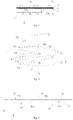
- the vehicle 1000 may be a fuel vehicle, a gas vehicle or a new energy vehicle that may be a pure electric vehicle, a hybrid vehicle or an extended-range vehicle.
- a battery 2000, a controller 3000 and a motor 4000 may be arranged inside the vehicle 1000, and the controller 3000 is used to control the battery 2000 to supply power to the motor 4000.
- the battery 2000 may be arranged at the bottom or the front or rear of the vehicle 1000.
- the battery 2000 can be used for supplying power of the vehicle 1000, for example, the battery 2000 being used as an operating power source of the vehicle 1000, and for the circuit system of the vehicle 1000, for example, for starting, navigating and running of the vehicle 1000.
- the battery 2000 can not only be used as the operating power source of the vehicle 1000, but also can be used as a driving power source of the automobile 4000 to provide driving power for the vehicle 1000 in place of or partially in place of fuel or natural gas.
- the battery may include a plurality of battery cells which may be connected in series or in parallel or in mixed connection that refers to the mixture of the series connection and the parallel connection.
- the plurality of battery cells can be connected in series or in parallel or in mixed connection to form a battery module, and then a plurality of battery modules can be connected in series or in parallel or in mixed connection to form the battery.
- the plurality of battery cells can form the battery directly, or form the battery module first, and then the battery modules can form the battery.
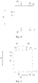
- the battery 2000 includes one or more battery modules 2010.
- the battery 2000 includes the plurality of battery modules 2010, and the plurality of battery modules 2010 can be connected in series or in parallel or in mixed.
- the mixed connection refers to the mixture of the series connection and the parallel connection.
- the battery 2000 may further include a box body 2020 (or a cover body), the box body 2020 has a hollow structure inside, and the plurality of battery modules 2010 are accommodated in the box body 2020. As shown in Fig.
- the box body 2020 includes two parts, which are referred to here as a first part 2021 and a second part 2022 respectively, and the first part 2021 and the second part 2022 are closed opposite to each other.
- the shapes of the first part 2021 and the second part 2022 may be determined according to the combined shape of the plurality of battery modules 2010, and each of the first part 2021 and the second part 2022 may have an opening.
- each of the first part 2021 and the second part 2022 can be a rectangular parallelepiped with a hollow inside and only one of its surfaces open, and with the opening of the first part 2021 and the opening of the second part 2022 arranged opposite to each other, the first part 2021 and the second part 2022 are coupled with each other to form a box body 2020 with a closed cavity.
- the plurality of battery modules 2010 are combined and connected in parallel or in series or in mixed connection, they are placed in a box body 2020 enclosed by the first part 2021 and the second part 2022 coupled with each other.
- the battery 2000 may also include other structures, which will not be repeated here.
- the battery 2000 may further include a confluence portion, which is used to realize the electrical connection among the plurality of battery cells, such as connection in parallel or in series or mixed.
- the confluence portion may realize electrical connection among the battery cells by connecting electrode terminals of the battery cells.
- the confluence portion may be fixed to the electrode terminals of the battery cells by welding.
- the electrical energy of the plurality of battery cells can be further drawn out through the box body 2020 through an electricity-conducting mechanism.
- the electricity-conducting mechanism may also belong to the bussing member.
- the battery module 2010 may include one or more battery cells. As shown in Fig. 3 , the battery module 2010 includes a plurality of battery cells 2011 which can be connected in series, in parallel or in mixed connection to achieve the larger capacity or power. Optionally, the battery module 2010 further includes the confluence portion 2012, and the confluence portion 2012 is used to realize the electrical connection (for example, in parallel, in series, or in mixed connection) among the plurality of battery cells 2011.
- the battery cell includes a lithium-ion secondary battery, a lithium-ion primary battery, a lithium-sulfur battery, a sodium-lithium-ion battery or a magnesium-ion battery, but is not limited thereto.
- the battery cell may be in the shape of cylinder, flat body, cuboid or other shapes. For example, as shown in Fig. 3 , the battery cell is in the shape of a cuboid structure.
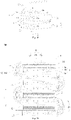
- Fig. 4 is an exploded structure schematic view of a battery cell disclosed in an embodiment of the present application.
- the battery cell 2011 of the embodiment in the present application includes a housing 20, an electrode assembly 10 arranged in the chousing 20, a cover plate 30 connected to the housing 20 and an electrode terminal 40 arranged at the cover plate 30 and electrically connected to the electrode assembly 10.
- the housing 20 in the embodiment of the present application is in a shape of a cuboid structure or other shapes.
- the housing 20 has an inner space that accommodates the electrode assembly 10 and electrolyte, and an opening communicating with the inner space.
- the housing 20 may be made of the material such as the aluminum, the aluminum alloy, the plastic or the like.
- the cover plate 30 in the embodiment of the present application has an outer surface and an inner surface opposite to each other and an electrode lead-out hole penetrating the outer surface and the inner surface.
- the cover plate 30 can cover an opening of the housing 20 and be connected with the housing 20 in a sealed manner.
- the inner surface of the cover plate 30 faces towards the electrode assembly 10.
- the electrode terminal 40 is arranged at the cover plate 30 and is arranged corresponding to the electrode lead-out hole. A part of the electrode terminal 40 is exposed on the outer surface of the cover plate 30 and is used for welding with the confluence portion.
- the battery cell 2011 further includes an adapter sheet 50, and the adapter sheet 50 is used to connect the electrode assembly 10 and the electrode terminal 40.
- the applicant found that at least one of the positive electrode sheet and the negative electrode sheet in the formed electrode assembly deviates from a predetermined position, so that it can affect the electrochemical performance of the battery cell.
- the applicant further found that at least one of the positive electrode sheet and the negative electrode sheet in the formed electrode assembly deviates from the predetermined position, resulting in lithium deposition in the electrode assembly, thereby affecting the electrochemical performance of the battery cell. It can be speculated that the reason may be that a size of a portion of the negative electrode sheet extending out of the outer edge of the positive electrode sheet is too small or the negative electrode sheet does not extend out of the outer edge of the positive electrode sheet.
- the applicant further studied the lithium deposition phenomenon and found that, taking the negative electrode sheet arranged continuously and the positive electrode sheet arranged to be spaced from one another as an example, it is difficult for the negative electrode sheet to be bent along the predetermined region during the bending process. As a result, after the positive electrode sheet and the negative electrode sheet are stacked to form the electrode assembly, the size of the portion of the negative electrode sheet extending out of the outer edge of the positive electrode sheet is too small, which is likely to cause the lithium deposition in the electrode assembly, thereby affecting the electrochemical performance and safety performance of the battery cell.
- the applicant improves the structure of the electrode assembly, and the embodiments of the present application are further described below.
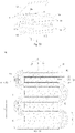
- Fig. 5 schematically discloses a schematic crosssectional view of an electrode assembly.
- the electrode assembly 10 includes a first electrode sheet 11 and a second electrode sheet 12, and a polarity of the second electrode sheet 12 is opposite to a polarity of the first electrode sheet 11.
- the electrode assembly 10 further includes two separators 13, and the first electrode sheet 11 is arranged between the two separators 13.
- the separators 13 can separate the first electrode sheet 11 from the second electrode sheet 12 to avoid the short circuit caused by the direct conduction between the first electrode sheet and the second electrode sheet.
- the first electrode sheet 11 is the negative electrode sheet
- the second electrode sheet 12 is the positive electrode sheet; alternatively, the first electrode sheet 11 can also be the positive electrode sheet, and the second electrode sheet 12 can be the negative electrode sheet.
- the first electrode sheet 11 includes an insulating substrate 11a, an electricity-conducting layer 11b arranged on a surface of the insulating substrate 11a and an active material layer 11c coating on a surface of the electricity-conducting layer 11b.
- the insulating substrate 11a can be made of the high molecular polymer material such as PP, PE, PET, or PI, which are resistant to corrosion by the electrolyte.
- the electricity-conducting layer 11b can be the metal base material; the active material layer 11c includes the active material.
- the first electrode sheet 11 is the negative electrode sheet, the electricity-conducting layer 11b of the negative electrode sheet is made of the copper base material, and the active material layer 11c of the negative electrode sheet includes the graphite or silicon.
- each of two surfaces of the insulating substrate 11a is provided with the electricity-conducting layer 11b.
- the second electrode sheet 12 includes an insulating substrate 12a, an electricity-conducting layer 12b arranged at the surface of the insulating substrate 12a and an active material layer 12c coating on a surface of the electricity-conducting layer 12b.
- the insulating substrate 12a can be made of the high molecular polymer material such as PP, PE, PET, or PI, which are resistant to corrosion by the electrolyte.
- the electricity-conducting layer 12b can be the metal base material; the active material layer 12c includes the active material.
- the second electrode sheet 12 is the positive electrode sheet
- the electricity-conducting layer 12b of the positive electrode sheet is made of the aluminum base material
- the active material layer 12c of the positive electrode sheet includes the lithium manganate, the lithium iron phosphate or the ternary material.
- each of two surfaces of the insulating substrate 12a is provided with the electricity-conducting layer 12b.
- the second electrode sheet 12 includes a metal current collector and an active material layer coating on the surface of the metal current collector, and the metal current collector is used to replace the insulating substrate 12a and the electricity-conducting layer 12b.
- the first electrode sheet 11 is bent to form a multi-layer structure and includes a plurality of bending segments 111 and a plurality of first layer-stacking segments 112 arranged to be stacked. Each of the bending segments 111 is used to connect two adjacent first layer-stacking segments 112.
- the first electrode sheet 11 is a continuous extending structure as a whole, and is cyclically bent in a "Z" shape. After the first electrode sheet 11 is bent into the multi-layer structure, the bending segments 111 are at least partially in a bent state.
- Each of the bending segments 111 has a guiding portion 113 for guiding the bending segment 111 to be bent during production. The guiding portion 113 can at least reduce the stiffness of a partial region of the bending segment 111 to guide the bending segment 111 to be bent during production.
- each of the bending segments 111 includes a weak region 114 and a connecting region 115.
- the weak region 114 is formed by arranging the guiding portion 113 on the bending segment 111. Compared with the connecting region 115, the weak region 114 is easier to be bent.
- the guiding portion 113 includes a groove 113a, and the groove 113a can reduce a thickness of the weak region 114, thereby making the weak region 114 easier to be bent.
- the weak region 114 is connected between the two connecting regions 115, and each of the connecting regions 115 is connected to a corresponding one of the first layer-stacking segments 112; in an alternative embodiment, there are two weak regions 114, the connecting region 115 is connected between the two weak regions 114 , and each of weak regions 114 is connected to a corresponding one of the first layer-stacking segments 112.
- the second electrode sheet 12 includes a plurality of second layer-stacking segments 121, and the plurality of second layer-stacking segments 121 and the plurality of first layer-stacking segments 112 are arranged alternately in a stacking direction of the first layer-stacking segments 112.
- the bending segments 111 and the second layer-stacking segments 121 do not have an overlapping region with each other.
- the bending segments 111 are completely in the bent state, and starting lines of the bending segments 111 are the regions where the bending segments start bending relative to the first layer-stacking segments 112.
- the edges of the first layer-stacking segments 112 extend out of the edges of the second layer-stacking segments 121.
- the groove 113a on each of bending segments 111 is arranged at an inner surface of the bending segment 111, in other words, the groove 113a is recessed with respect to the inner side surface of the bending segment 111.
- the inner side surface refers to a surface of the bending segment 111 close to the second layer-stacking segment 121.
- an outer surface of the bending segment 111 refers to a surface of the bending segment 111 away from the second layer-stacking segment 121.
- the groove 113a on each of the bending segments 111 is located at the side of the insulating substrate 11a close to the second layer-stacking segment 121. In this embodiment, the groove 113a is formed in a middle region of the bending segment 111.
- Fig. 6 schematically shows a partial structure of the first electrode sheet 11 in an unfolded state.
- the first electrode sheet 11 includes the plurality of bending segments 111 which are at least partially in the bent state after being bent and the plurality of first layer-stacking segments 112.
- the first electrode sheet 11 is a continuous extension structure as a whole.
- the bending segments 111 and the first layer-stacking segments 112 are arranged alternately.
- Each of the bending segments 111 is connected to two adjacent first layer-stacking segments 112.
- each of the first layer-stacking segments 112 has two first outer edges 116 opposite to each other, and each of the bending segments 111 has two second outer edges 117 opposite to each other.
- the first direction X is the same as the width direction of the first electrode sheet 11.
- the first direction X is perpendicular to the extending direction W.
- the first outer edge 116 and the second outer edge 117 at the same side are flush with each other.
- the first electrode sheet 11 also has a first tab 118 extending out of the first outer edge 116 of the first layer-stacking segment 112 in the first direction X; the first tab 118 includes the insulating substrate 11a and the electricity-conducting layer 11b arranged on the surface of the insulating substrate 11a, and the electricity-conducting layer 11b is at least partially uncoated with the active material layer 11c.
- the number and positions of the first tabs 118 are arranged in a one-to-one correspondence with the number and positions of the first layer-stacking segments 112.
- the number of the guiding portions 113 may be the same as the number of the bending segments 111.
- the bending segments 111 of all the bending segments 111 are provided with the guiding portions 113, while other bending segments 111 may not be provided with the guiding portions 113.
- the guiding portions 113 are used to guide the bending segments 111 to be bent during production. During the production process, when an external force is applied to the first electrode sheet 11 to perform the bending operation, since the guiding portions 113 are arranged on the bending segments 111, the bending segments 111 can be more easily bent in the region where the guiding portions 113 are located.
- the guiding portions 113 are arranged in the first direction X.
- each of the guiding portions 113 includes the groove 113a extending in the first direction X.
- Fig. 7 schematically shows a cross-segmental structure of the first electrode sheet 11 of the embodiment shown in Fig. 6 .
- the first electrode sheet 11 includes the insulating substrate 11a, an electricity-conducting layer 11b arranged on the surface of the insulating substrate 11a, and the active material layer 11c coating on the surface of the electricity-conducting layer 11b.
- the insulating substrate 11a has two surfaces opposite to each other in a thickness direction H of the first electrode sheet 11.
- the two electricity-conducting layers 11b are respectively arranged on the two surfaces, and each of the electricity-conducting layers 11b is coated with an active material layer 11c.
- the insulating substrate 11a can be made of the high molecular polymer material such as PP, PE, PET or PI, which is resistant to corrosion by the electrolyte.
- the electricity-conducting layer 12b is made of the aluminum base material, and the active material layer 12c includes lithium manganate, lithium iron phosphate or a ternary material.
- the electricity-conducting layer 11b adopts the copper base material, and the active material layer 11c includes graphite or silicon.
- the guiding portion 113 may be a trace left by things.
- it may refer to a structure formed after removing a part of the active material layer 11c on the first electrode sheet 11 by a material removing member, or a structure formed by removing a part of the active material layer 11c and a part of the electricity-conducting layer 11b on the first electrode sheet 11, or a structure formed by removing a part of the active material layer 11c, a part of the electricity-conducting layer 11b and a part of the insulating substrate 11a on the first electrode sheet 11.
- each of the bending segments 111 is provided with the guiding portion 113.
- the guiding portion 113 includes a groove 113a.
- the grooves 113a are recessed and extended in a direction from the surface of the first electrode sheet 11 towards the insulating substrate 11a in the thickness direction H of the first electrode sheet 11.
- the groove 113a arranged in one bending segment 111 is located at one side of the insulating substrate 11a, and the groove 113a arranged in the other bending segment 111 is located at the other side of the insulating substrate 11a.
- the grooves 113a may be formed by removing a part of the active material layer 11c and a part of the electricity-conducting layer 11b on the first electrode sheet 11. Alternatively, when the electricity-conducting layer 11b is formed on the insulating substrate 11a, the electricity-conducting layer 11b can be omitted at a corresponding position. In this embodiment, the groove 113a penetrates the electricity-conducting layer 11b and exposes the insulating substrate 11a; alternatively, in the thickness direction H, the depth of the groove 113a may be equal to the sum of the thicknesses of the active material layer 11c and the thicknesses of the electricity-conducting layer 11b.
- the groove 113a extends to the surface of the insulating substrate 11a, but does not extend into the insulating substrate 11a. However, it can be understood that the depth of the groove 113a can also be less than or equal to the thickness of the active material layer 11c, so that the groove 113a does not penetrate the electricity-conducting layer 11b in the thickness direction H, at this time, an electricity-conducting layer 11b is further arranged between the groove 113a and the insulating substrate 11a.
- the grooves 113a When the depth of the grooves 113a is less than or equal to the thickness of the active material layer 11c, the grooves 113a will not damage the electricity-conducting layer 11b, and the adjacent first layer-stacking segments 112 can be electrically connected through the electricity-conducting layers 11b of the bending segments 111.
- an orthographic projection of the groove 113a on a plane perpendicular to the first direction X may be a rectangle.
- the orthographic projection of the groove 113a may be not limited to a rectangle, or may be a U-shape or a V-shape.
- a mouth portion of the groove 113a is greater than or equal to a bottom of the groove 113a, which, on the one hand, is beneficial to ensuring the proper bending positions of the bending segments 111 and also the ease of forming the groove 113a, and which, on the other hand, allows the electrode active material near the mouth portion of the groove 113a to be subjected to a less or no extrusion stress during the bending process, so that the bending resistance of the first layer-stacking segments 112 can be reduced, making bending easier and more accurate to a predetermined position.
- the grooves 113a are continuously arranged and extend to the two second outer edges 117 of the bending segment 111 opposite to each other so as to penetrate the entire bending segment 111.
- the electrode active material near the groove 113a can be subjected to the less or no squeezing stress, so that the bending resistance of the first layer-stacking segment 112 can be reduced, and therefore, the accuracy of the bending position of the bending segment 111 can be better ensured, which further ensures that the first layer-stacking segment 112 can be more easily and more accurately bent to a predetermined position.
- the bending segment 111 has a part of the active material layer 11c. One of the two active material layers 11c is not completely removed, and the other layer may or may not be completely removed.
- the opening size of the groove 113a is smaller than the size of the bending segment 111, as a result of which, the other regions on the bending segment 111 than the guiding portion 113 can be covered by the active material layer 11c.
- both two active material layers 11c are completely removed.
- the size of the guiding portion 113 in the first direction X can be set according to the size of the bending segment 111 in the first direction X.
- the size of the guiding portion 113 in the first direction X is the length of the guide portion 113.
- the size of the bending segment 111 in the first direction X is also the length of the bending segment 111. Therefore, in some other embodiments, the groove 113a does not penetrate through the bending segment 111 in the first direction X.
- the ratio of the size of the groove 113a in the first direction X to the size of the bending segment 111 in the first direction X may be 0.4 to 0.8, preferably 0.4, 0.5, 0.6, 0.7 or 0.8.
- Fig. 8 schematically shows the structure of the first electrode sheet 11 of the embodiment shown in Fig. 6 that is in a state of multiple reciprocating fold.
- the first electrode sheet 11 needs to be bent.
- the guiding portion 113 can guide the bending segment 111 to be bent; in other words, the bending segment 111 can be bent along the guiding portion 113, so that the bending position can be located at a predetermined position, and it is beneficial to ensure that the first outer edges 116 of the two adjacent first layer-stacking segments 112 can be consistent.
- the bending segment 111 of the first electrode sheet 11 can be bent in the bending direction Z as shown in Fig. 8 .
- the bending direction Z and the first direction X are perpendicular to each other, that is, the plane where the bending direction Z is located and the first direction X are perpendicular to each other.
- the first electrode sheet 11 may be reciprocatingly bent substantially in a zigzag.
- the dashed line shown in Fig. 8 does not represent a physical structure, but schematically shows a dividing line between the bending segment 111 and the first layer-stacking segment 112.
- the two adjacent grooves 113a are located on two surfaces of the first electrode sheet 11 opposite to each other, and the grooves 113a are located at the side of the bending segment 111 that is subjected to the extrusion stress when the bending segment 111 is bent, after the first electrode sheet 11 is bent, the opening of the groove 113 a on the bending segment 111 faces to a space formed between two adjacent first layer-stacking segments 112; that is, the groove 113a is located on the inner surface of the bending segment 111, so that a side of the weak region 114 close to the groove 113a does not bear a tensile stress, thereby reducing the possibility of breaking under the action of the tensile stress in the weak region 114.
- first layer-stacking segments 112 can be stacked and arranged spaced from one another in a second direction Y, and the space formed between the two adjacent first layer-stacking segments 112 can be used to accommodate the second layer-stacking segments 121 of the second electrode sheet 12.
- the second direction Y is the same as a stacking direction of the first layer-stacking segment 112 and is perpendicular to the first direction X.
- the bending segment 111 may be in a shape of an arc, such as a circular arc.
- the separators 13 are respectively arranged at two sides of the first electrode sheet 11 opposite to each other.
- the two separators 13 are arranged in pairs, and the first electrode sheet 11 is arranged between the two separators 13.
- the separators 13 cover the first layer-stacking segment 112 and the bending segment 111.
- the two separators 13 each are attached to the first electrode sheet 11 by a corresponding feeding equipment.
- the second electrode sheet 12 is arranged at the side of the separator 13 away from the first electrode sheet 11.
- the polarity of the first electrode sheet 11 and the polarity of the second electrode sheet 12 are opposite, and when one of the electrode sheets is the positive electrode sheet, the other one is the negative electrode sheet.
- the second electrode sheet 12 includes the plurality of second layer-stacking segments 121.
- two adjacent second layer-stacking segments 121 are respectively arranged at two sides of the first electrode sheet 11 opposite to each other.
- the first layer-stacking segment 112 and the second layer-stacking segment 121 are positioned corresponding to each other.
- a second layer-stacking segment 121 is arranged between the two adj acent bending segments 111.
- the present application does not limit the second layer-stacking segment 121 arranged between two adjacent bending segments 111, and the suitable number of the second layer-stacking segments 121 may also be provided according to the product requirements.
- the second layer-stacking segment 121 is attached to the separator 13.
- the second layer-stacking segment 121 and the separator 13 may be connected by thermal compression, electrophoresis or adhesive.
- the separator 13 is an insulator arranged between the first electrode sheet 11 and the second electrode sheet 12.
- the material of the separator 13 may be an insulating material such as the plastic or the like, so as to insulate and isolate the first electrode sheet 11 and the second electrode sheet 12.
- first electrode sheet 11 the separators 13 and the second electrode sheet 12 are combined according to the mode as shown in Fig. 9 , the bending segment 111 can be bent under the guidance by the guiding portion 113, and finally the bent state as shown in Fig. 5 can be formed.
- Fig. 10 schematically shows a top-view structure after the first layer-stacking segment 112 and the second layer-stacking segment 121 are stacked.
- the first electrode sheet 11 is the negative electrode sheet
- the second electrode sheet 12 is the positive electrode sheet.
- the expression that the second layer-stacking segment 121 is entirely covered by the first layer-stacking segment 112 means that an orthographic projection of the second layer-stacking segment 121 in the second direction Y is completely within an orthographic projection of the first layer-stacking segment 112 in the second direction Y, and then the projected area of the second layer-stacking segment 121 is smaller than the projected area of the first layer-stacking segment 112.
- the distance between the first outer edge 116 of the first layer-stacking segment 112 and a third outer edge 122 of the corresponding second layer-stacking segment 121 is greater than or equal to 0.2 mm and less than or equal to 5 mm, preferably 0.5 mm, 1mm, 1.5mm, 2mm, 2.5mm, 3mm, 3.5mm, 4mm or 4.5mm. Since the bending segment 111 is provided with the guiding portion 113, the first electrode sheet 11 is bent under the guiding action of the guiding portion 113, so that the respective first outer edges 116 of the two adjacent first layer-stacking segments 112 connected with the bending segment 111 are consistent.
- the expression that the respective first outer edges 116 of the two adjacent first layer-stacking segments 112 are consistent includes the state shown in Fig. 10 , that is, in the second direction Y, the orthographic projections of the two adjacent first layer-stacking segments 112 coincide with each other.
- the angle ⁇ between the two first outer edges 116 of the two adjacent first layer-stacking segments 112 at the same side is 0°, therefore, in the top-view state, the respective first outer edges 116 of the two adjacent first layer-stacking segments 112 are aligned with each other and kept consistent.
- the consistency of the respective first outer edges 116 of the two adjacent first layer-stacking segments 112 also includes the state shown in Fig. 11.
- Fig. 11 schematically shows another top-view structure after the first layer-stacking segment 112 and the second layer-stacking segment 121 are stacked.
- the two first outer edges 116 of the two adjacent first layer-stacking segments 112 at the same side in the top-view state are not completely aligned with each other.
- the angle ⁇ is greater than 0° and less than or equal to 30° to ensure that the first layer-stacking segment 112 covers the second layer-stacking segment 121.
- the value of the angle ⁇ is 5°, 10°, 15°, 20° or 25°.
- the angle ⁇ is an allowable error angle.
- the first outer edge 116 of the first layer-stacking segment 112 which has been bent is offset so as to fail to coincide with the first outer edge 116 of another first layer-stacking segment 112; however, it can still be ensured that when the first layer-stacking segment 112 covers the second layer-stacking segment 121, the angle ⁇ between the two first outer edges 116 of two adjacent first layer-stacking segments 112 at the same side can refer to the allowable error angle.
- the first electrode sheet 11 of the embodiment of the application due to arranging the guiding portion 113 in the bending segment 111, in the production process of the electrode assembly 10, when the first electrode sheet 11 is subjected to a bending operation, under the guiding action of the guiding portion 113 , the first electrode sheet 11 is more easily bent in the region of the guiding portion 113 of the bending segment 111, so that the controllability and accuracy of the bending position of the bending segment 111 can be improved by arranging the guiding portion 113, thereby improving the consistency of the first outer edges 116 of the two adjacent first layer-stacking segments 112.
- the possibility can be reduced that one of the first layer-stacking segment 112 and the second layer-stacking segment 121 as the negative electrode may not completely cover the other one as the positive electrode due to the randomness of the bending position after the first electrode sheet 11 is bent, so as to reduce the possibility of lithium deposition in the fabricated electrode assembly 10.
- the active material layer 11c itself has a certain brittleness. During the bending process of the bending segment 111, the active material layer 11c will be subjected to an external force, so that the active material layer 11c may fall off or drop the powder from the electricity-conducting layer 11b, which can affect the electrochemical performance and safety performance of the electrode assembly 10.
- the grooves 113a are formed by reducing the corresponding active material layers 11c, so that during the bending process of the bending segment 111, the provided grooves 113a are beneficial to reducing the internal stress borne by the corresponding active material layer 11c, thereby reducing the possibility that the active material layer 11c falls off or drops powder.
- the first electrode sheet 11 in the embodiment of the present application utilizes the composite structure of the insulating substrate 11a and the electricity-electricity-conducting layer 11b to replace the traditional metal current collector, which can further reduce the bending difficulty of the first electrode sheet 11, thereby improving the controllability and the accuracy of the bending position of the bending segment 111, and improving the consistency of the first outer edges 116 of the two adjacent first layer-stacking segments 112.
- a thickness of the insulating substrate 11a may be 1 ⁇ m-20 ⁇ m, and a thickness of the electricity-electricity-conducting layer 11b may be 0.1 ⁇ m-10 ⁇ m.
- the burr generated by the electricity-electricity-conducting layer 11b at a pierced position is also small, and it is difficult for the burr to pierce the separator 13, which can reduce the risk of short circuit and improve safety performance.
- Fig. 12 schematically shows a cross-segmental view of an electrode assembly 100 according to another embodiment of the present application.
- the guiding portion 113 includes a groove 113a.
- the groove 113a is recessed and extended from the inner surface of the bending segment 111 toward the insulating substrate 11a.
- the opening of the groove 113 a faces to the second layer-stacking segment 121.
- the groove 113a penetrates the inner active material layer 11c and the inner electricity-electricity-conducting layer 11b in the thickness direction H of the first electrode sheet 11, and in the extending direction W of the first electrode sheet 11, the size of the groove 113a is equal to the size of the bending segment 111.
- the portions of the inner active material layer 11c and the inner electricity-conducting layer 11b corresponding to the bending segment 111 are completely removed, so that the surface of the insulating substrate 11a facing to the second layer-stacking segment 121 may be exposed.
- the portions of the outer active material layer 11c and the outer electricity-conducting layer 11b corresponding to the bending segment 111 are not removed but completely retained.
- the rigidity of the bending segment 111 can be further reduced, so that the bending segment 111 is easy to be bent at the guiding portion 113, thereby effectively preventing the inner active material layer 11c from falling off or dropping powder after the bending segment 111 has been bent.
- the portions of the outer active material layer 11c and the outer electricity-conducting layer 11b corresponding to the bending segment 111 may be partially removed to form the groove 113a on the outer active material layer 11c.
- Fig. 13 schematically shows a cross-segmental view of an electrode assembly 200 according to another embodiment of the present application.
- the electrode assembly 200 of the embodiment shown in Fig. 13 the structures same as the electrode assembly 10 of the embodiment shown in Fig. 5 will not be repeated here.
- the differences from the electrode assembly 10 of the embodiment shown in Fig. 5 are mainly described here.
- the guiding portion 113 includes the groove 113a, and the groove 113a is arranged on the outer surface of the bending portion 111.
- Fig. 14 schematically shows a cross-segmental view of an electrode assembly 300 according to another embodiment of the present application.
- the structure same as that of the electrode assembly 10 of the embodiment shown in Fig. 5 will not be repeated here.
- the differences from the electrode assembly 10 of the embodiment shown in Fig. 5 are mainly described here.
- each of the bending segments 111 is correspondingly provided with a guiding portion 113.
- the guiding portion 113 includes two grooves 113a. When the first electrode sheet 11 is in the unfolded state, the two grooves 113a are correspondingly arranged in the thickness direction H of the first electrode sheet 11.
- one of the two grooves 113a is arranged on the outer surface of the bending segment 111 so as to face away from the space formed between the two adjacent first layer-stacking segments 112, and the other is arranged on the inner surface of the bending segment 111 so as to face to the space formed between the two adjacent first layer-stacking segments 112.
- two grooves 113a are arranged in the thickness direction H, and the thickness of the weak region 114 is smaller in this case, so that it is beneficial to further reducing the rigidity of the weak region 114.
- the bending segment 111 is more likely to be bent in the weak region 114 where the grooves 113a are arranged, so that it is beneficial to further improving the controllability of the bending position and the accuracy.
- the internal stress of its own will be smaller, so that it is beneficial to further reducing the difficulty of bending, and reducing the possibility that the active material layers 11c falls off or drops powder from the electricity-conducting layer 11b due to the tensile or the compressive stress.
- the structures of the two grooves 113a are the same.
- Fig. 15 schematically shows a cross-segmental view of an electrode assembly 400 according to another embodiment of the present application.
- the structures same as the electrode assembly 300 of the embodiment shown in Fig. 14 will not be repeated here.
- the differences from the electrode assembly 10 of the embodiment shown in Fig. 14 are mainly described here.
- only the insulating substrate 11a is arranged on each bending segment 111.
- each bending segment 111 is correspondingly provided with a guiding portion 113.
- the guiding portion 113 includes two grooves 113a.
- the active material layer 11c and the electricity-conducting layer 11b on the inner side of the insulating substrate 11a are completely removed, so that the surface of the insulating substrate 11a facing to the second layer-stacking segment 121 can be exposed; the electricity-conducting layer 11b and the active material layer 11c on the outer side of the insulating substrate 11a are all removed, so that the surface of the insulating substrate 11a facing away from the second layer-stacking segment 121 can be exposed.
- the rigidity of the bending segment 111 can be further reduced, so that the bending segment 111 is easily bent at the guiding portion 113, so as to effectively prevent the active material layer 11c at the inside from falling off or dropping powder after the bending segment 111 has been bent.
- Fig. 16 schematically shows a cross-segmental view of an electrode assembly 500 according to another embodiment of the present application.
- the electrode assembly 500 of the embodiment shown in Fig. 16 the structure same as the electrode assembly 400 of the embodiment shown in Fig. 15 will not be repeated here.
- the differences from the electrode assembly 10 of the embodiment shown in Fig. 14 are mainly described here.
- the groove 113a also extends to a part of the insulating substrate 11a after penetrating the active material layer 11c and the electricity-conducting layer 11b.
- a part of the groove 113a is allowed to be recessed into the insulating substrate 11a.
- a part of the insulating substrate 11a can be removed to form a part of the groove 113a, so that it is beneficial to further reduce the rigidity of the bending segment 111, and the bending segment 111 can be easier to be bent under the guidance of the guiding portion 113.
- Fig. 17 schematically shows a cross-segmental view of an electrode assembly 600 according to another embodiment of the present application
- Fig. 18 shows the structure of the first electrode sheet of Fig. 17 in the bent state.
- the electrode assembly 600 of the embodiment shown in Fig. 17 the structure same as the electrode assembly 10 of the embodiment shown in Fig. 5 will not be repeated here.
- the differences from the electrode assembly 10 of the embodiment shown in Fig. 5 are mainly described here.
- the guiding portion 113 includes more than two grooves 113a. In the first direction X, two or more grooves 113a are arranged to be spaced from one another.
- the weak regions 114 when the first electrode sheet 11 is in the unfolded state, in the thickness direction H of the first electrode sheet 11, the weak regions 114 can be arranged corresponding to the grooves 113a.
- the number and positions of the weak regions 114 are set in a one-to-one correspondence with the number and positions of the grooves 113a.
- the orthographic projection of each of the grooves 113a on a plane perpendicular to the first direction X may be a rectangle.
- the orthographic projection of the groove 113a is not limited to the rectangle, but can also be a trapezoid or a triangle.
- each of the grooves 113a extends from the inner surface of the bending segment 111 toward the insulating substrate 11a, so that the opening of the groove 113a faces towards the second layer-stacking segment 121.
- the ratio of the sum of the sizes of the respective grooves 113a in the first direction X to the size of the bending segment 111 in the first direction X is 0.4 to 0.8, preferably 0.4, 0.5, 0.6, 0.7 or 0.8.
- each of the grooves 113a extends from the outer surface of the bending segment 111 toward the insulating substrate 11a, so that the opening of the groove 113a can face away from the second layer-stacking segment 121.
- a plurality of grooves 113a are arranged on each of the inner surface and the outer surface of the bending segment 111.
- the positions of the grooves 113a on the inner surface and the grooves 113a on the outer surface correspond to each other.
- the positions of the weak regions 114 are arranged in a one-to-one correspondence with the positions of the grooves 113a on the inner surface and the positions of the grooves 113a on the outer surface.
- the grooves 113a on the inner surface and the grooves 113a on the outer surface jointly correspond one weak region 114.
- Fig. 19 schematically shows a cross-segmental view of an electrode assembly 700 according to another embodiment of the present application
- Fig. 20 shows the structure of the first electrode sheet of Fig. 19 in the bent state.
- the electrode assembly 700 of the embodiment shown in Fig. 19 the structure same as the electrode assembly 10 of the embodiment shown in Fig. 5 will not be repeated here.
- the differences from the electrode assembly 10 of the embodiment shown in Fig. 5 are mainly described here.
- the guiding portion 113 includes two or more through holes 113b. In the first direction X, two or more through holes 113b are arranged to be spaced from one another.
- the through holes 113b penetrate through two active material layers 11c, the two electricity-conducting layers 11b and the insulating substrate 11a.
- the size of the through hole 113b in the extending direction W of the first electrode sheet 11 is smaller than the size of the bending segment 111 in the extending direction W of the first electrode sheet 11.
- the shape of the through hole 113b may be a rectangle, a square, an ellipse, a trapezoid or a triangle.
- the ratio of the sum of the sizes of the through holes 113b in the first direction X to the size of the bending segment 111 in the first direction X is 0.4 to 0.8, preferably 0.6 or 0.7.
- the guiding portion 113 includes the through holes 113b.
- the ratio of the sizes of the through holes 113b in the first direction X to the size of the bending segment 111 in the first direction X is 0.4 to 0.8, preferably 0.6 or 0.7.
- the through holes 113b on the bending segment 111 which has been bent are arranged to correspond to a middle region of the second layer-stacking segment 121.
- the present application does not limit the positions of the through holes 113b, and the positions of the through holes 113b may also be set to correspond to other regions of the second layer-stacking segment 121 that are deviated from the middle region in the second direction Y.
- Fig. 21 schematically shows a schematic cross-segmental view of an electrode assembly 800 according to another embodiment of the present application
- Fig. 22 shows the structure of the first electrode sheet of Fig. 21 in a bent state.
- the electrode assembly 800 of the embodiment shown in Fig. 21 the structure same as the electrode assembly 700 of the embodiment shown in Fig. 19 will not be repeated here.
- the differences from the electrode assembly 700 of the embodiment shown in Fig. 19 are mainly described here.
- the guiding portion 113 includes two or more grooves 113a and two or more through holes 113b.
- one or two or more grooves 113a may be arranged between two adjacent through holes 113b.
- one or two or more through holes 113b may be arranged between two adjacent grooves 113a.
- the guiding portion 113 may include other numbers of grooves 113a and other numbers of through holes 113b according to the requirement.
- the guiding portion 113 may include one groove 113a and one through hole 113b. As shown in Fig.
- each groove 113a extends from the outer surface of the bending segment 111 toward the insulating substrate 11a, so that the opening of the groove 113a faces away from the second layer-stacking segment 121; on the other bending segment 111, each groove 113a extends from the inner surface of the bending segment 111 toward the insulating substrate 11a, so that the opening of the groove 113a can face to the second layer-stacking segment 121.
- each groove 113a on each bending segment 111 extends from the outer surface of the bending segment 111 toward the insulating substrate 11a, so that the opening of the groove 113a can face away from the second layer-stacking segment 121.
- each groove 113a on each bending segment 111 extends from the outer surface of the bending segment 111 toward the insulating substrate 11a, so that the opening of the groove 113a can face the second layer-stacking segment 121.
Landscapes
- Chemical & Material Sciences (AREA)
- Chemical Kinetics & Catalysis (AREA)
- Electrochemistry (AREA)
- General Chemical & Material Sciences (AREA)
- Engineering & Computer Science (AREA)
- Manufacturing & Machinery (AREA)
- Materials Engineering (AREA)
- Connection Of Batteries Or Terminals (AREA)
- Secondary Cells (AREA)
- Cell Electrode Carriers And Collectors (AREA)
- Battery Electrode And Active Subsutance (AREA)
Abstract
Description
- This application claims priority to
Chinese Patent Application No. 202022087154.2, titled "ELECTRODE ASSEMBLY, BATTERY CELL, BATTERY, AND ELECTRICITY-CONSUMING DEVICE" and filed on September 22, 2020 - The present application relates to the technical field of batteries, and in particular, to an electrode assembly, a battery cell, a battery and an electricity-consuming device.
- With the development of society, science and technology, a battery is widely used to supply power to high-power devices, such as an electric vehicle. The battery achieves greater capacity or power by connecting a plurality of battery cells in series or in parallel.
- The battery cell includes a positive electrode sheet and a negative electrode sheet, and the positive electrode sheet and the negative electrode sheet are stacked to form an electrode assembly. However, during a stacking process, the positive electrode sheet and the negative electrode sheet are easily deviated from predetermined positions, thereby affecting the electrochemical performance of the battery cells.
- The present application provides an electrode assembly, a battery cell, a battery and an electricity-consuming device, which can reduce the dislocation of an electrode sheet and reduce the risk of the lithium deposition.
- In a first aspect, an embodiment of the present application provides an electrode assembly for a battery, including: a first electrode sheet including an insulating substrate, an electricity-conducting layer arranged on a surface of the insulating substrate, and an active material layer coating on a surface of the electricity-conducting layer, in which the first electrode sheet is bent to form a multi-layer structure and includes a plurality of bending segments and a plurality of first layer-stacking segments arranged to be stacked, each of the bending segments is configured to connect two adjacent first layer-stacking segments, and each of the bending segments includes a guiding portion for guiding the bending segment to be bent during production; a second electrode sheet, in which a polarity of the second electrode sheet is opposite to a polarity of the first electrode sheet, and the second electrode sheet includes a plurality of second layer-stacking segments, the plurality of second layer-stacking segments and the plurality of first layer-stacking segments are alternately arranged in a layer-stacking direction of the first layer-stacking segments.
- According to an aspect of the embodiments of the present application, the guiding portion is arranged in a first direction, and the first direction is perpendicular to a bending direction of the bending segments.
- According to an aspect of the embodiments of the present application, each of the first layer-stacking segments includes two first outer edges opposite to each other; after the bending segments is guided to be bent during production, the first outer edges of the two adjacent first layer-stacking segments connected to the bending segments are consistent.
- According to an aspect of the embodiments of the present application, the guiding portion includes at least one groove and/or at least one through hole.
- According to an aspect of the embodiments of the present application, when the guiding portion includes only one groove, in a first direction perpendicular to a bending direction of the bending segment, the groove is arranged continuously and penetrates the bending segment.
- According to an aspect of the embodiments of the present application, when the guiding portion includes a plurality of grooves and/or a plurality of through holes, the plurality of grooves and/or the plurality of through holes are arranged to be spaced from one another.
- According to an aspect of the embodiments of the present application, the groove is arranged on a surface of the bending segment close to the second layer-stacking segments.
- According to an aspect of the embodiments of the present application, the groove penetrates the electricity-conducting layer and exposes the insulating substrate.
- According to an aspect of the embodiments of the present application, when the guiding portion includes the through hole, the through hole penetrates the bending segment.
- According to an aspect of the embodiments of the present application, only the insulating substrate is arranged on each of the bending segments.
- In a second aspect, an embodiment of the present application provides a battery cell including the electrode assembly as described in the first aspect.
- In a third aspect, an embodiment of the present application provides a battery including the battery cell as described in the second aspect.
- In a fourth aspect, an embodiment of the present application provides an electricity-consuming device including the battery as described in the third aspect, in which the battery is configured to provide electrical energy.
- In the electrode assembly in the embodiment of the present application, since the guiding portion is arranged at bending segment in the first electrode sheet, during the production process of the electrode assembly, when the first electrode sheet is bent, the first electrode sheet is easier to be bent in a region of the guiding portion of the bending segment under a guiding action of the guiding portion. Therefore, the controllability and accuracy of a bending position of the bending segment can be improved by arranging the guiding portion, thereby improving the consistency of the first outer edges of the two adjacent first layer-stacking segments. The possibility can be reduced that one of the first layer-stacking segment and the second layer-stacking segment as the negative electrode cannot completely cover the other one as the positive electrode due to the randomness of the bending position when the first electrode has been bent, so that the possibility of lithium deposition in the fabricated electrode assembly can be reduced. In addition, the first electrode sheet takes a composite structure composed of an insulating substrate and a electricity-conducting layer to replace a traditional metal current collector, so that it can further reduce the difficulty of bending the first electrode sheet and improve the controllability and accuracy of the bending position of the bending segment, thereby improving the uniformity of the first outer edges of the two adjacent first layer-stacking segments.
- Features, advantages, and technical effects of exemplary embodiments of the present application will be described below with reference to the drawings.
-
Fig 1 shows a schematic structural view of a vehicle according to an embodiment of the present application; -
Fig. 2 shows a schematic view of an exploded structure of a battery according to an embodiment of the present application; -
Fig. 3 shows a partial schematic structure view of a battery module according to an embodiment of the present application; -
Fig. 4 shows an exploded structure schematic view of a battery cell according to an embodiment of the present application; -
Fig. 5 shows a schematic cross-segmental view of an electrode assembly according to an embodiment of the present application; -
Fig. 6 shows a partial structure schematic top view of a first electrode sheet that has not been bent in the embodiment shown inFig. 5 ; -
Fig. 7 shows a side view structure schematic view of the first electrode sheet in the embodiment shown inFig. 6 ; -
Fig. 8 shows a schematic structural view of the first electrode sheet in the embodiment shown inFig. 6 in a bent state; -
Fig. 9 shows a schematic view of a first electrode sheet, a second electrode sheet and an separator that have not been bent in the embodiment shown inFig. 5 ; -
Fig. 10 shows a schematic top view of a first structure of an electrode assembly in the embodiment shown inFig. 5 ; -
Fig. 11 shows a schematic top view of a second structure of an electrode assembly in the embodiment shown inFig. 5 ; -
Figs. 12 to 17 respectively show schematic cross-segmental views of electrode assemblies according to various embodiments of the present application; -
Fig. 18 shows a schematic structural view of a first electrode sheet as shown inFig. 17 in a bent state; -
Fig. 19 shows a schematic cross-segmental view of an electrode assembly according to another embodiment of the present application; -
Fig. 20 shows a schematic structural view of a first electrode as shown inFig. 19 in a bent state; -
Fig. 21 shows a schematic cross-segmental view of an electrode assembly according to another embodiment of the present application; -
Fig. 22 shows a schematic structural view of a first electrode sheet as shown inFig. 21 in a bent state. - In the drawings, the drawings are not drawn to actual scale.
- Reference number:
- 10. electrode assembly; 20. housing; 30. top cover plate; 40. electrode terminal; 50. adapter sheet;
- 11. first electrode sheet; 11a, insulating substrate; 11b, electricity-conducting layer; 11c, active material layer; 111, bending segment; 112, first layer-stacking segment; 113, guiding portion; 113a, groove; 113b. through hole; 114, weak region; 115, connecting region; 116, first outer edge; 117, second outer edge; 118, first tab;
- 12. second electrode sheet; 12a. insulating substrate; 12b, electricity-conducting layer; 12c. active material layer; 121, second layer-stacking segment; 122; third outer edge; 123. second tab;
- 13. separator;
- 100, 200, 300, 400, 500, 600, 700, 800: electrode assembly;
- 1000. vehicle; 2000. battery; 2010. battery module; 2011. battery cell; 2012. confluence portion; 2020. box body; 2021. first part; 2022. second part; 3000, controller; 4000, motor;
- W, extending direction; H, thickness direction; X, first direction; Y, second direction; Z, bending direction.
- The implementation of the present application will be described in further detail below in conjunction with the drawings and embodiments. The detailed description and drawings of the embodiments below are used to exemplarily illustrate the principle of the present application, but cannot be used to limit the scope of the present application, that is, the present application can be not limited to the described embodiments.
- In the description of the present application, it should be noted that, unless otherwise specified, "plurality" means more than two; the terms "upper", "lower", "left", "right", "inner", "outer", etc. indicate the orientation or positional relationship only for the convenience of describing the present application and simplifying the description, rather than indicating or implying that the device or the element referred to must have a specific orientation, be configured and operated in a specific orientation, and therefore cannot be understood as a limitation of the present application. In addition, the terms "first", "second", "third", etc. are only used for descriptive purposes, and shall not be understood as indicating or implying relative importance. The term "perpendicular" does not mean strictly perpendicular, but allows for an error within the allowable range. The term "parallel" does not mean strictly parallel, but allows for an error within the allowable range.
- The "embodiment" referred in the present application means that a particular feature, a structure, or a characteristic described in connection with the embodiment can be included in at least one embodiment of the present application. The appearances of the phrase in various positions in the specification are not necessarily all referring to the same embodiment, nor a separate or alternative embodiment that is mutually exclusive of other embodiments. It is explicitly and implicitly understood by those skilled in the art that the embodiments described in the present application may be combined with other embodiments.
- In the description of the present application, it should also be noted that, unless otherwise clearly specified and limited, the terms "mount", "communicate" and "connect" should be understood in a broad sense, for example, it can be a fixed connection, a detachable connection, or an integral connection, it can be a direct connection, or it can be connected indirectly through an intermediary. For those of ordinary skill in the art, the specific meaning of the above-mentioned terms in the present application can be understood according to specific situations.
- A battery cell and a battery described in the embodiments of the present application are adapted to various devices using the battery, such as a mobile phone, a portable device, a notebook computer, a storage-battery car, an electric vehicle, a ship, a spacecraft, an electric toy, an electric tool and the like; for example, the spacecraft includes an airplane, a rocket, a space shuttle and a spacecraft and the like, the electric toy includes a stationary or mobile electric toy, such as a game console, an electric car toy, an electric ship toy and an electric airplane toy and the like; and the power tool includes a metal cutting power tool, a grinding power tool, an assembly power tool and a railway power tool, such as a power drill, a power grinder, a power wrench, a power screwdriver, a hammer, an impact drill, a concrete vibrator and a power planer.
- The battery cell and battery described in the embodiments of the present application are not only adapted to the above-described electrical device, but can also be applied to all devices using battery. However, for the sake of brevity, the following embodiments take an electric vehicle as an example to illustrate.
- For example, as shown in
Fig. 1 which is a schematic structural view of avehicle 1000 according to an embodiment of the present application, thevehicle 1000 may be a fuel vehicle, a gas vehicle or a new energy vehicle that may be a pure electric vehicle, a hybrid vehicle or an extended-range vehicle. Abattery 2000, acontroller 3000 and amotor 4000 may be arranged inside thevehicle 1000, and thecontroller 3000 is used to control thebattery 2000 to supply power to themotor 4000. For example, thebattery 2000 may be arranged at the bottom or the front or rear of thevehicle 1000. Thebattery 2000 can be used for supplying power of thevehicle 1000, for example, thebattery 2000 being used as an operating power source of thevehicle 1000, and for the circuit system of thevehicle 1000, for example, for starting, navigating and running of thevehicle 1000. In another embodiment of the present application, thebattery 2000 can not only be used as the operating power source of thevehicle 1000, but also can be used as a driving power source of theautomobile 4000 to provide driving power for thevehicle 1000 in place of or partially in place of fuel or natural gas. - In order to meet different usage power requirements, the battery may include a plurality of battery cells which may be connected in series or in parallel or in mixed connection that refers to the mixture of the series connection and the parallel connection. Optionally, the plurality of battery cells can be connected in series or in parallel or in mixed connection to form a battery module, and then a plurality of battery modules can be connected in series or in parallel or in mixed connection to form the battery. In other words, the plurality of battery cells can form the battery directly, or form the battery module first, and then the battery modules can form the battery.
- In another embodiment of the present application, as shown in
Fig. 2 which is an exploded structure schematic view of thebattery 2000 according to an embodiment of the present application, thebattery 2000 includes one ormore battery modules 2010. For example, thebattery 2000 includes the plurality ofbattery modules 2010, and the plurality ofbattery modules 2010 can be connected in series or in parallel or in mixed. The mixed connection refers to the mixture of the series connection and the parallel connection. Thebattery 2000 may further include a box body 2020 (or a cover body), thebox body 2020 has a hollow structure inside, and the plurality ofbattery modules 2010 are accommodated in thebox body 2020. As shown inFig. 2 , thebox body 2020 includes two parts, which are referred to here as afirst part 2021 and asecond part 2022 respectively, and thefirst part 2021 and thesecond part 2022 are closed opposite to each other. The shapes of thefirst part 2021 and thesecond part 2022 may be determined according to the combined shape of the plurality ofbattery modules 2010, and each of thefirst part 2021 and thesecond part 2022 may have an opening. For example, each of thefirst part 2021 and thesecond part 2022 can be a rectangular parallelepiped with a hollow inside and only one of its surfaces open, and with the opening of thefirst part 2021 and the opening of thesecond part 2022 arranged opposite to each other, thefirst part 2021 and thesecond part 2022 are coupled with each other to form abox body 2020 with a closed cavity. After the plurality ofbattery modules 2010 are combined and connected in parallel or in series or in mixed connection, they are placed in abox body 2020 enclosed by thefirst part 2021 and thesecond part 2022 coupled with each other. - Optionally, the
battery 2000 may also include other structures, which will not be repeated here. For example, thebattery 2000 may further include a confluence portion, which is used to realize the electrical connection among the plurality of battery cells, such as connection in parallel or in series or mixed. Specifically, the confluence portion may realize electrical connection among the battery cells by connecting electrode terminals of the battery cells. Further, the confluence portion may be fixed to the electrode terminals of the battery cells by welding. The electrical energy of the plurality of battery cells can be further drawn out through thebox body 2020 through an electricity-conducting mechanism. Optionally, the electricity-conducting mechanism may also belong to the bussing member. - According to different power requirements, the
battery module 2010 may include one or more battery cells. As shown inFig. 3 , thebattery module 2010 includes a plurality ofbattery cells 2011 which can be connected in series, in parallel or in mixed connection to achieve the larger capacity or power. Optionally, thebattery module 2010 further includes theconfluence portion 2012, and theconfluence portion 2012 is used to realize the electrical connection (for example, in parallel, in series, or in mixed connection) among the plurality ofbattery cells 2011. For example, the battery cell includes a lithium-ion secondary battery, a lithium-ion primary battery, a lithium-sulfur battery, a sodium-lithium-ion battery or a magnesium-ion battery, but is not limited thereto. The battery cell may be in the shape of cylinder, flat body, cuboid or other shapes. For example, as shown inFig. 3 , the battery cell is in the shape of a cuboid structure. -
Fig. 4 is an exploded structure schematic view of a battery cell disclosed in an embodiment of the present application. Referring toFig. 4 , thebattery cell 2011 of the embodiment in the present application includes ahousing 20, anelectrode assembly 10 arranged in thechousing 20, acover plate 30 connected to thehousing 20 and anelectrode terminal 40 arranged at thecover plate 30 and electrically connected to theelectrode assembly 10. - The
housing 20 in the embodiment of the present application is in a shape of a cuboid structure or other shapes. Thehousing 20 has an inner space that accommodates theelectrode assembly 10 and electrolyte, and an opening communicating with the inner space. Thehousing 20 may be made of the material such as the aluminum, the aluminum alloy, the plastic or the like. - The
cover plate 30 in the embodiment of the present application has an outer surface and an inner surface opposite to each other and an electrode lead-out hole penetrating the outer surface and the inner surface. Thecover plate 30 can cover an opening of thehousing 20 and be connected with thehousing 20 in a sealed manner. The inner surface of thecover plate 30 faces towards theelectrode assembly 10. Theelectrode terminal 40 is arranged at thecover plate 30 and is arranged corresponding to the electrode lead-out hole. A part of theelectrode terminal 40 is exposed on the outer surface of thecover plate 30 and is used for welding with the confluence portion. Optionally, thebattery cell 2011 further includes anadapter sheet 50, and theadapter sheet 50 is used to connect theelectrode assembly 10 and theelectrode terminal 40. - After noticing the problem of the poor electrochemical performance of the battery cell in the related art, the applicant found that at least one of the positive electrode sheet and the negative electrode sheet in the formed electrode assembly deviates from a predetermined position, so that it can affect the electrochemical performance of the battery cell. The applicant further found that at least one of the positive electrode sheet and the negative electrode sheet in the formed electrode assembly deviates from the predetermined position, resulting in lithium deposition in the electrode assembly, thereby affecting the electrochemical performance of the battery cell. It can be speculated that the reason may be that a size of a portion of the negative electrode sheet extending out of the outer edge of the positive electrode sheet is too small or the negative electrode sheet does not extend out of the outer edge of the positive electrode sheet.
- By analyzing the assembly process of the electrode assembly, the applicant further studied the lithium deposition phenomenon and found that, taking the negative electrode sheet arranged continuously and the positive electrode sheet arranged to be spaced from one another as an example, it is difficult for the negative electrode sheet to be bent along the predetermined region during the bending process. As a result, after the positive electrode sheet and the negative electrode sheet are stacked to form the electrode assembly, the size of the portion of the negative electrode sheet extending out of the outer edge of the positive electrode sheet is too small, which is likely to cause the lithium deposition in the electrode assembly, thereby affecting the electrochemical performance and safety performance of the battery cell.
- Based on the above problems discovered by the applicant, the applicant improves the structure of the electrode assembly, and the embodiments of the present application are further described below.
- In some optional embodiments,
Fig. 5 schematically discloses a schematic crosssectional view of an electrode assembly. Referring toFig. 5 , theelectrode assembly 10 includes afirst electrode sheet 11 and asecond electrode sheet 12, and a polarity of thesecond electrode sheet 12 is opposite to a polarity of thefirst electrode sheet 11. Theelectrode assembly 10 further includes twoseparators 13, and thefirst electrode sheet 11 is arranged between the twoseparators 13. Theseparators 13 can separate thefirst electrode sheet 11 from thesecond electrode sheet 12 to avoid the short circuit caused by the direct conduction between the first electrode sheet and the second electrode sheet. Optionally, thefirst electrode sheet 11 is the negative electrode sheet, and thesecond electrode sheet 12 is the positive electrode sheet; alternatively, thefirst electrode sheet 11 can also be the positive electrode sheet, and thesecond electrode sheet 12 can be the negative electrode sheet. - The
first electrode sheet 11 includes an insulatingsubstrate 11a, an electricity-conductinglayer 11b arranged on a surface of the insulatingsubstrate 11a and anactive material layer 11c coating on a surface of the electricity-conductinglayer 11b. The insulatingsubstrate 11a can be made of the high molecular polymer material such as PP, PE, PET, or PI, which are resistant to corrosion by the electrolyte. The electricity-conductinglayer 11b can be the metal base material; theactive material layer 11c includes the active material. Optionally, thefirst electrode sheet 11 is the negative electrode sheet, the electricity-conductinglayer 11b of the negative electrode sheet is made of the copper base material, and theactive material layer 11c of the negative electrode sheet includes the graphite or silicon. In some embodiments, each of two surfaces of the insulatingsubstrate 11a is provided with the electricity-conductinglayer 11b. - Optionally, the
second electrode sheet 12 includes an insulatingsubstrate 12a, an electricity-conductinglayer 12b arranged at the surface of the insulatingsubstrate 12a and anactive material layer 12c coating on a surface of the electricity-conductinglayer 12b. The insulatingsubstrate 12a can be made of the high molecular polymer material such as PP, PE, PET, or PI, which are resistant to corrosion by the electrolyte. The electricity-conductinglayer 12b can be the metal base material; theactive material layer 12c includes the active material. Optionally, thesecond electrode sheet 12 is the positive electrode sheet, the electricity-conductinglayer 12b of the positive electrode sheet is made of the aluminum base material, and theactive material layer 12c of the positive electrode sheet includes the lithium manganate, the lithium iron phosphate or the ternary material. In some embodiments, each of two surfaces of the insulatingsubstrate 12a is provided with the electricity-conductinglayer 12b. - In some embodiments, the
second electrode sheet 12 includes a metal current collector and an active material layer coating on the surface of the metal current collector, and the metal current collector is used to replace the insulatingsubstrate 12a and the electricity-conductinglayer 12b. - The
first electrode sheet 11 is bent to form a multi-layer structure and includes a plurality of bendingsegments 111 and a plurality of first layer-stackingsegments 112 arranged to be stacked. Each of the bendingsegments 111 is used to connect two adjacent first layer-stackingsegments 112. Thefirst electrode sheet 11 is a continuous extending structure as a whole, and is cyclically bent in a "Z" shape. After thefirst electrode sheet 11 is bent into the multi-layer structure, the bendingsegments 111 are at least partially in a bent state. Each of the bendingsegments 111 has a guidingportion 113 for guiding thebending segment 111 to be bent during production. The guidingportion 113 can at least reduce the stiffness of a partial region of thebending segment 111 to guide thebending segment 111 to be bent during production. - Optionally, each of the bending
segments 111 includes aweak region 114 and a connectingregion 115. Theweak region 114 is formed by arranging the guidingportion 113 on thebending segment 111. Compared with the connectingregion 115, theweak region 114 is easier to be bent. For example, the guidingportion 113 includes agroove 113a, and thegroove 113a can reduce a thickness of theweak region 114, thereby making theweak region 114 easier to be bent. - In some embodiments, there are two connecting
regions 115, theweak region 114 is connected between the two connectingregions 115, and each of the connectingregions 115 is connected to a corresponding one of the first layer-stackingsegments 112; in an alternative embodiment, there are twoweak regions 114, the connectingregion 115 is connected between the twoweak regions 114 , and each ofweak regions 114 is connected to a corresponding one of the first layer-stackingsegments 112. - The
second electrode sheet 12 includes a plurality of second layer-stackingsegments 121, and the plurality of second layer-stackingsegments 121 and the plurality of first layer-stackingsegments 112 are arranged alternately in a stacking direction of the first layer-stackingsegments 112. In the stacking direction of the first layer-stackingsegments 112, the bendingsegments 111 and the second layer-stackingsegments 121 do not have an overlapping region with each other. In the embodiment, the bendingsegments 111 are completely in the bent state, and starting lines of the bendingsegments 111 are the regions where the bending segments start bending relative to the first layer-stackingsegments 112. In a direction parallel to the second layer-stackingsegments 121, the edges of the first layer-stackingsegments 112 extend out of the edges of the second layer-stackingsegments 121. There are gaps between the bendingsegments 111 and the second layer-stackingsegments 121, and ends of the second layer-stackingsegments 121 do not contact with the bendingsegments 111, so as to reduce the possibility that the active material falls off or drops powder from the ends of the second layer-stackingsegments 121 due to conflict between the ends and the bending segments. - Optionally, after the
first electrode sheet 11 has been bent, thegroove 113a on each of bendingsegments 111 is arranged at an inner surface of thebending segment 111, in other words, thegroove 113a is recessed with respect to the inner side surface of thebending segment 111. Here, the inner side surface refers to a surface of thebending segment 111 close to the second layer-stackingsegment 121. Correspondingly, an outer surface of thebending segment 111 refers to a surface of thebending segment 111 away from the second layer-stackingsegment 121. Further optionally, thegroove 113a on each of the bendingsegments 111 is located at the side of the insulatingsubstrate 11a close to the second layer-stackingsegment 121. In this embodiment, thegroove 113a is formed in a middle region of thebending segment 111. -
Fig. 6 schematically shows a partial structure of thefirst electrode sheet 11 in an unfolded state. Referring toFig. 6 , thefirst electrode sheet 11 includes the plurality of bendingsegments 111 which are at least partially in the bent state after being bent and the plurality of first layer-stackingsegments 112. Thefirst electrode sheet 11 is a continuous extension structure as a whole. In an extending direction W of thefirst electrode sheet 11 itself, the bendingsegments 111 and the first layer-stackingsegments 112 are arranged alternately. Each of the bendingsegments 111 is connected to two adjacent first layer-stackingsegments 112. In a first direction X, each of the first layer-stackingsegments 112 has two firstouter edges 116 opposite to each other, and each of the bendingsegments 111 has two secondouter edges 117 opposite to each other. The first direction X is the same as the width direction of thefirst electrode sheet 11. The first direction X is perpendicular to the extending direction W. In the embodiment, in the first direction X, the firstouter edge 116 and the secondouter edge 117 at the same side are flush with each other. Thefirst electrode sheet 11 also has afirst tab 118 extending out of the firstouter edge 116 of the first layer-stackingsegment 112 in the first direction X; thefirst tab 118 includes the insulatingsubstrate 11a and the electricity-conductinglayer 11b arranged on the surface of the insulatingsubstrate 11a, and the electricity-conductinglayer 11b is at least partially uncoated with theactive material layer 11c. Optionally, the number and positions of thefirst tabs 118 are arranged in a one-to-one correspondence with the number and positions of the first layer-stackingsegments 112. In the embodiment, the number of the guidingportions 113 may be the same as the number of the bendingsegments 111. Of course, it can be understood that some of the bendingsegments 111 of all the bendingsegments 111 are provided with the guidingportions 113, while other bendingsegments 111 may not be provided with the guidingportions 113. The guidingportions 113 are used to guide the bendingsegments 111 to be bent during production. During the production process, when an external force is applied to thefirst electrode sheet 11 to perform the bending operation, since the guidingportions 113 are arranged on the bendingsegments 111, the bendingsegments 111 can be more easily bent in the region where the guidingportions 113 are located. Therefore, it is beneficial to improving the controllability and accuracy of the bending positions, thereby ensuring that thefirst electrode sheet 11 and thesecond electrode sheet 12 are respectively at predetermined positions, and ensuring that the battery cell has good electrochemical performance. The guidingportions 113 are arranged in the first direction X. Optionally, each of the guidingportions 113 includes thegroove 113a extending in the first direction X. -
Fig. 7 schematically shows a cross-segmental structure of thefirst electrode sheet 11 of the embodiment shown inFig. 6 . Thefirst electrode sheet 11 includes the insulatingsubstrate 11a, an electricity-conductinglayer 11b arranged on the surface of the insulatingsubstrate 11a, and theactive material layer 11c coating on the surface of the electricity-conductinglayer 11b. The insulatingsubstrate 11a has two surfaces opposite to each other in a thickness direction H of thefirst electrode sheet 11. The two electricity-conductinglayers 11b are respectively arranged on the two surfaces, and each of the electricity-conductinglayers 11b is coated with anactive material layer 11c. The insulatingsubstrate 11a can be made of the high molecular polymer material such as PP, PE, PET or PI, which is resistant to corrosion by the electrolyte. In an example, when thefirst electrode sheet 11 is the positive electrode sheet, the electricity-conductinglayer 12b is made of the aluminum base material, and theactive material layer 12c includes lithium manganate, lithium iron phosphate or a ternary material. When thefirst electrode sheet 11 is the negative electrode sheet, the electricity-conductinglayer 11b adopts the copper base material, and theactive material layer 11c includes graphite or silicon. The guidingportion 113 may be a trace left by things. Alternatively, it may refer to a structure formed after removing a part of theactive material layer 11c on thefirst electrode sheet 11 by a material removing member, or a structure formed by removing a part of theactive material layer 11c and a part of the electricity-conductinglayer 11b on thefirst electrode sheet 11, or a structure formed by removing a part of theactive material layer 11c, a part of the electricity-conductinglayer 11b and a part of the insulatingsubstrate 11a on thefirst electrode sheet 11. - In this embodiment, each of the bending
segments 111 is provided with the guidingportion 113. In this embodiment, the guidingportion 113 includes agroove 113a. Thegrooves 113a are recessed and extended in a direction from the surface of thefirst electrode sheet 11 towards the insulatingsubstrate 11a in the thickness direction H of thefirst electrode sheet 11. In the twoadjacent bending segments 111, thegroove 113a arranged in onebending segment 111 is located at one side of the insulatingsubstrate 11a, and thegroove 113a arranged in theother bending segment 111 is located at the other side of the insulatingsubstrate 11a. Thegrooves 113a may be formed by removing a part of theactive material layer 11c and a part of the electricity-conductinglayer 11b on thefirst electrode sheet 11. Alternatively, when the electricity-conductinglayer 11b is formed on the insulatingsubstrate 11a, the electricity-conductinglayer 11b can be omitted at a corresponding position. In this embodiment, thegroove 113a penetrates the electricity-conductinglayer 11b and exposes the insulatingsubstrate 11a; alternatively, in the thickness direction H, the depth of thegroove 113a may be equal to the sum of the thicknesses of theactive material layer 11c and the thicknesses of the electricity-conductinglayer 11b. Thegroove 113a extends to the surface of the insulatingsubstrate 11a, but does not extend into the insulatingsubstrate 11a. However, it can be understood that the depth of thegroove 113a can also be less than or equal to the thickness of theactive material layer 11c, so that thegroove 113a does not penetrate the electricity-conductinglayer 11b in the thickness direction H, at this time, an electricity-conductinglayer 11b is further arranged between thegroove 113a and the insulatingsubstrate 11a. When the depth of thegrooves 113a is less than or equal to the thickness of theactive material layer 11c, thegrooves 113a will not damage the electricity-conductinglayer 11b, and the adjacent first layer-stackingsegments 112 can be electrically connected through the electricity-conductinglayers 11b of the bendingsegments 111. - In an example, an orthographic projection of the
groove 113a on a plane perpendicular to the first direction X may be a rectangle. However, the orthographic projection of thegroove 113a may be not limited to a rectangle, or may be a U-shape or a V-shape. Optionally, a mouth portion of thegroove 113a is greater than or equal to a bottom of thegroove 113a, which, on the one hand, is beneficial to ensuring the proper bending positions of the bendingsegments 111 and also the ease of forming thegroove 113a, and which, on the other hand, allows the electrode active material near the mouth portion of thegroove 113a to be subjected to a less or no extrusion stress during the bending process, so that the bending resistance of the first layer-stackingsegments 112 can be reduced, making bending easier and more accurate to a predetermined position. - Referring to
Fig. 5 to Fig. 7 , in the first direction X, thegrooves 113a are continuously arranged and extend to the two secondouter edges 117 of thebending segment 111 opposite to each other so as to penetrate theentire bending segment 111. Compared with the case where thegroove 113a does not penetrate theentire bending segment 111, during the bending process, the electrode active material near thegroove 113a can be subjected to the less or no squeezing stress, so that the bending resistance of the first layer-stackingsegment 112 can be reduced, and therefore, the accuracy of the bending position of thebending segment 111 can be better ensured, which further ensures that the first layer-stackingsegment 112 can be more easily and more accurately bent to a predetermined position. In this embodiment, thebending segment 111 has a part of theactive material layer 11c. One of the twoactive material layers 11c is not completely removed, and the other layer may or may not be completely removed. In this embodiment, in the extending direction W of thefirst electrode sheet 11, the opening size of thegroove 113a is smaller than the size of thebending segment 111, as a result of which, the other regions on thebending segment 111 than the guidingportion 113 can be covered by theactive material layer 11c. In an example, in theweak region 114, both twoactive material layers 11c are completely removed. - The size of the guiding
portion 113 in the first direction X can be set according to the size of thebending segment 111 in the first direction X. The size of the guidingportion 113 in the first direction X is the length of theguide portion 113. The size of thebending segment 111 in the first direction X is also the length of thebending segment 111. Therefore, in some other embodiments, thegroove 113a does not penetrate through thebending segment 111 in the first direction X. The ratio of the size of thegroove 113a in the first direction X to the size of thebending segment 111 in the first direction X may be 0.4 to 0.8, preferably 0.4, 0.5, 0.6, 0.7 or 0.8. -
Fig. 8 schematically shows the structure of thefirst electrode sheet 11 of the embodiment shown inFig. 6 that is in a state of multiple reciprocating fold. During the manufacturing process of theelectrode assembly 10, thefirst electrode sheet 11 needs to be bent. During production, the guidingportion 113 can guide thebending segment 111 to be bent; in other words, thebending segment 111 can be bent along the guidingportion 113, so that the bending position can be located at a predetermined position, and it is beneficial to ensure that the firstouter edges 116 of the two adjacent first layer-stackingsegments 112 can be consistent. Thebending segment 111 of thefirst electrode sheet 11 can be bent in the bending direction Z as shown inFig. 8 . The bending direction Z and the first direction X are perpendicular to each other, that is, the plane where the bending direction Z is located and the first direction X are perpendicular to each other. In this embodiment, thefirst electrode sheet 11 may be reciprocatingly bent substantially in a zigzag. The dashed line shown inFig. 8 does not represent a physical structure, but schematically shows a dividing line between the bendingsegment 111 and the first layer-stackingsegment 112. Since the twoadjacent grooves 113a are located on two surfaces of thefirst electrode sheet 11 opposite to each other, and thegrooves 113a are located at the side of thebending segment 111 that is subjected to the extrusion stress when thebending segment 111 is bent, after thefirst electrode sheet 11 is bent, the opening of thegroove 113 a on thebending segment 111 faces to a space formed between two adjacent first layer-stackingsegments 112; that is, thegroove 113a is located on the inner surface of thebending segment 111, so that a side of theweak region 114 close to thegroove 113a does not bear a tensile stress, thereby reducing the possibility of breaking under the action of the tensile stress in theweak region 114. After thefirst electrode sheet 11 is folded, two adjacent first layer-stackingsegments 112 can be stacked and arranged spaced from one another in a second direction Y, and the space formed between the two adjacent first layer-stackingsegments 112 can be used to accommodate the second layer-stackingsegments 121 of thesecond electrode sheet 12. The second direction Y is the same as a stacking direction of the first layer-stackingsegment 112 and is perpendicular to the first direction X. In this embodiment, thebending segment 111 may be in a shape of an arc, such as a circular arc. - In the embodiment as shown in
Fig. 9 , based on thefirst electrode sheet 11, in the thickness direction H of thefirst electrode sheet 11, theseparators 13 are respectively arranged at two sides of thefirst electrode sheet 11 opposite to each other. The twoseparators 13 are arranged in pairs, and thefirst electrode sheet 11 is arranged between the twoseparators 13. Theseparators 13 cover the first layer-stackingsegment 112 and thebending segment 111. During the production process, the twoseparators 13 each are attached to thefirst electrode sheet 11 by a corresponding feeding equipment. Thesecond electrode sheet 12 is arranged at the side of theseparator 13 away from thefirst electrode sheet 11. The polarity of thefirst electrode sheet 11 and the polarity of thesecond electrode sheet 12 are opposite, and when one of the electrode sheets is the positive electrode sheet, the other one is the negative electrode sheet. Thesecond electrode sheet 12 includes the plurality of second layer-stackingsegments 121. In this embodiment, two adjacent second layer-stackingsegments 121 are respectively arranged at two sides of thefirst electrode sheet 11 opposite to each other. In the thickness direction H, the first layer-stackingsegment 112 and the second layer-stackingsegment 121 are positioned corresponding to each other. In this embodiment, a second layer-stackingsegment 121 is arranged between the two adjacent bending segments 111. However, the present application does not limit the second layer-stackingsegment 121 arranged between twoadjacent bending segments 111, and the suitable number of the second layer-stackingsegments 121 may also be provided according to the product requirements. In an example, after theseparators 13 are arranged on thefirst electrode sheet 11, the second layer-stackingsegment 121 is attached to theseparator 13. For example, the second layer-stackingsegment 121 and theseparator 13 may be connected by thermal compression, electrophoresis or adhesive. Theseparator 13 is an insulator arranged between thefirst electrode sheet 11 and thesecond electrode sheet 12. The material of theseparator 13 may be an insulating material such as the plastic or the like, so as to insulate and isolate thefirst electrode sheet 11 and thesecond electrode sheet 12. - After
first electrode sheet 11, theseparators 13 and thesecond electrode sheet 12 are combined according to the mode as shown inFig. 9 , thebending segment 111 can be bent under the guidance by the guidingportion 113, and finally the bent state as shown inFig. 5 can be formed. -
Fig. 10 schematically shows a top-view structure after the first layer-stackingsegment 112 and the second layer-stackingsegment 121 are stacked. In this embodiment, thefirst electrode sheet 11 is the negative electrode sheet, and thesecond electrode sheet 12 is the positive electrode sheet. Under the guiding action of the guidingportion 113 on thebending segment 111, after thefirst electrode sheet 11 has been bent reciprocatingly, all of circumferential edges of the first layer-stackingsegment 112 extend out of the second layer-stackingsegment 121, thereby ensuring that the second stackingsegment 121 is entirely covered by the first layer-stackingsegment 112, and effectively reducing the possibility of lithium deposition caused by the second layer-stackingsegment 121 extending out of the first layer-stackingsegment 112. Herein, the expression that the second layer-stackingsegment 121 is entirely covered by the first layer-stackingsegment 112 means that an orthographic projection of the second layer-stackingsegment 121 in the second direction Y is completely within an orthographic projection of the first layer-stackingsegment 112 in the second direction Y, and then the projected area of the second layer-stackingsegment 121 is smaller than the projected area of the first layer-stackingsegment 112. In an example, the distance between the firstouter edge 116 of the first layer-stackingsegment 112 and a thirdouter edge 122 of the corresponding second layer-stackingsegment 121 is greater than or equal to 0.2 mm and less than or equal to 5 mm, preferably 0.5 mm, 1mm, 1.5mm, 2mm, 2.5mm, 3mm, 3.5mm, 4mm or 4.5mm. Since thebending segment 111 is provided with the guidingportion 113, thefirst electrode sheet 11 is bent under the guiding action of the guidingportion 113, so that the respective firstouter edges 116 of the two adjacent first layer-stackingsegments 112 connected with thebending segment 111 are consistent. In other words, there is an angle α between the two firstouter edges 116 of the two adjacent first layer-stackingsegments 112 at the same side. Herein, the expression that the respective firstouter edges 116 of the two adjacent first layer-stackingsegments 112 are consistent includes the state shown inFig. 10 , that is, in the second direction Y, the orthographic projections of the two adjacent first layer-stackingsegments 112 coincide with each other. The angle α between the two firstouter edges 116 of the two adjacent first layer-stackingsegments 112 at the same side is 0°, therefore, in the top-view state, the respective firstouter edges 116 of the two adjacent first layer-stackingsegments 112 are aligned with each other and kept consistent. The consistency of the respective firstouter edges 116 of the two adjacent first layer-stackingsegments 112 also includes the state shown inFig. 11. Fig. 11 schematically shows another top-view structure after the first layer-stackingsegment 112 and the second layer-stackingsegment 121 are stacked. The two firstouter edges 116 of the two adjacent first layer-stackingsegments 112 at the same side in the top-view state are not completely aligned with each other. There is an angle α between the two firstouter edges 116 of the two adjacent first layer-stackingsegments 112 at the same side. The angle α is greater than 0° and less than or equal to 30° to ensure that the first layer-stackingsegment 112 covers the second layer-stackingsegment 121. Preferably, the value of the angle α is 5°, 10°, 15°, 20° or 25°. Herein, the angle α is an allowable error angle. The firstouter edge 116 of the first layer-stackingsegment 112 which has been bent is offset so as to fail to coincide with the firstouter edge 116 of another first layer-stackingsegment 112; however, it can still be ensured that when the first layer-stackingsegment 112 covers the second layer-stackingsegment 121, the angle α between the two firstouter edges 116 of two adjacent first layer-stackingsegments 112 at the same side can refer to the allowable error angle. - In the
first electrode sheet 11 of the embodiment of the application, due to arranging the guidingportion 113 in thebending segment 111, in the production process of theelectrode assembly 10, when thefirst electrode sheet 11 is subjected to a bending operation, under the guiding action of the guidingportion 113 , thefirst electrode sheet 11 is more easily bent in the region of the guidingportion 113 of thebending segment 111, so that the controllability and accuracy of the bending position of thebending segment 111 can be improved by arranging the guidingportion 113, thereby improving the consistency of the firstouter edges 116 of the two adjacent first layer-stackingsegments 112. Therefore, the possibility can be reduced that one of the first layer-stackingsegment 112 and the second layer-stackingsegment 121 as the negative electrode may not completely cover the other one as the positive electrode due to the randomness of the bending position after thefirst electrode sheet 11 is bent, so as to reduce the possibility of lithium deposition in the fabricatedelectrode assembly 10. In addition, theactive material layer 11c itself has a certain brittleness. During the bending process of thebending segment 111, theactive material layer 11c will be subjected to an external force, so that theactive material layer 11c may fall off or drop the powder from the electricity-conductinglayer 11b, which can affect the electrochemical performance and safety performance of theelectrode assembly 10. In the present application, thegrooves 113a are formed by reducing the correspondingactive material layers 11c, so that during the bending process of thebending segment 111, the providedgrooves 113a are beneficial to reducing the internal stress borne by the correspondingactive material layer 11c, thereby reducing the possibility that theactive material layer 11c falls off or drops powder. - In addition, the
first electrode sheet 11 in the embodiment of the present application utilizes the composite structure of the insulatingsubstrate 11a and the electricity-electricity-conductinglayer 11b to replace the traditional metal current collector, which can further reduce the bending difficulty of thefirst electrode sheet 11, thereby improving the controllability and the accuracy of the bending position of thebending segment 111, and improving the consistency of the firstouter edges 116 of the two adjacent first layer-stackingsegments 112. - A thickness of the insulating
substrate 11a may be 1 µm-20 µm, and a thickness of the electricity-electricity-conductinglayer 11b may be 0.1 µm-10 µm. During the use of the battery cell, in the case that a foreign object pierces thefirst electrode sheet 11, since the thickness of the electricity-electricity-conductinglayer 11b is small, the burr generated by the electricity-electricity-conductinglayer 11b at a pierced position is also small, and it is difficult for the burr to pierce theseparator 13, which can reduce the risk of short circuit and improve safety performance. - In some other embodiments, the same structure as the embodiment shown in
Fig. 5 is not repeated here, and the difference from the embodiment shown inFig. 5 will be mainly described here. -
Fig. 12 schematically shows a cross-segmental view of anelectrode assembly 100 according to another embodiment of the present application. In theelectrode assembly 100 of the embodiment shown inFig. 12 , the structure same as that of theelectrode assembly 10 of the embodiment shown inFig. 5 will not be repeated here. The differences from theelectrode assembly 10 of the embodiment shown inFig. 5 are mainly described here. In this embodiment, the guidingportion 113 includes agroove 113a. Thegroove 113a is recessed and extended from the inner surface of thebending segment 111 toward the insulatingsubstrate 11a. The opening of thegroove 113 a faces to the second layer-stackingsegment 121. Thegroove 113a penetrates the inneractive material layer 11c and the inner electricity-electricity-conductinglayer 11b in the thickness direction H of thefirst electrode sheet 11, and in the extending direction W of thefirst electrode sheet 11, the size of thegroove 113a is equal to the size of thebending segment 111. The portions of the inneractive material layer 11c and the inner electricity-conductinglayer 11b corresponding to thebending segment 111 are completely removed, so that the surface of the insulatingsubstrate 11a facing to the second layer-stackingsegment 121 may be exposed. The portions of the outeractive material layer 11c and the outer electricity-conductinglayer 11b corresponding to thebending segment 111 are not removed but completely retained. Since theactive material layer 11c and the electricity-conductinglayer 11b at the inner side of thebending segment 111 are all removed, the rigidity of thebending segment 111 can be further reduced, so that thebending segment 111 is easy to be bent at the guidingportion 113, thereby effectively preventing the inneractive material layer 11c from falling off or dropping powder after thebending segment 111 has been bent. In some other embodiments, the portions of the outeractive material layer 11c and the outer electricity-conductinglayer 11b corresponding to thebending segment 111 may be partially removed to form thegroove 113a on the outeractive material layer 11c. -
Fig. 13 schematically shows a cross-segmental view of anelectrode assembly 200 according to another embodiment of the present application. In theelectrode assembly 200 of the embodiment shown inFig. 13 , the structures same as theelectrode assembly 10 of the embodiment shown inFig. 5 will not be repeated here. The differences from theelectrode assembly 10 of the embodiment shown inFig. 5 are mainly described here. In this embodiment, the guidingportion 113 includes thegroove 113a, and thegroove 113a is arranged on the outer surface of the bendingportion 111. -
Fig. 14 schematically shows a cross-segmental view of anelectrode assembly 300 according to another embodiment of the present application. In theelectrode assembly 300 of the embodiment shown inFig. 14 , the structure same as that of theelectrode assembly 10 of the embodiment shown inFig. 5 will not be repeated here. The differences from theelectrode assembly 10 of the embodiment shown inFig. 5 are mainly described here. In this embodiment, each of the bendingsegments 111 is correspondingly provided with a guidingportion 113. The guidingportion 113 includes twogrooves 113a. When thefirst electrode sheet 11 is in the unfolded state, the twogrooves 113a are correspondingly arranged in the thickness direction H of thefirst electrode sheet 11. In thefirst electrode sheet 11 which has been bent, one of the twogrooves 113a is arranged on the outer surface of thebending segment 111 so as to face away from the space formed between the two adjacent first layer-stackingsegments 112, and the other is arranged on the inner surface of thebending segment 111 so as to face to the space formed between the two adjacent first layer-stackingsegments 112. In this embodiment, for each of the bendingsegments 111, twogrooves 113a are arranged in the thickness direction H, and the thickness of theweak region 114 is smaller in this case, so that it is beneficial to further reducing the rigidity of theweak region 114. In this way, since the stiffness of theweak region 114 corresponding to the twogrooves 113a is relatively small, thebending segment 111 is more likely to be bent in theweak region 114 where thegrooves 113a are arranged, so that it is beneficial to further improving the controllability of the bending position and the accuracy. Thus, compared with thebending segment 111 without thegrooves 113a, when theactive material layers 11c at two sides in the embodiment are bent, the internal stress of its own will be smaller, so that it is beneficial to further reducing the difficulty of bending, and reducing the possibility that the active material layers 11c falls off or drops powder from the electricity-conductinglayer 11b due to the tensile or the compressive stress. In an example, the structures of the twogrooves 113a are the same. -
Fig. 15 schematically shows a cross-segmental view of anelectrode assembly 400 according to another embodiment of the present application. In theelectrode assembly 400 of the embodiment shown inFig. 15 , the structures same as theelectrode assembly 300 of the embodiment shown inFig. 14 will not be repeated here. The differences from theelectrode assembly 10 of the embodiment shown inFig. 14 are mainly described here. In this embodiment, only the insulatingsubstrate 11a is arranged on each bendingsegment 111. In this embodiment, each bendingsegment 111 is correspondingly provided with a guidingportion 113. The guidingportion 113 includes twogrooves 113a. At thebending segment 111, theactive material layer 11c and the electricity-conductinglayer 11b on the inner side of the insulatingsubstrate 11a are completely removed, so that the surface of the insulatingsubstrate 11a facing to the second layer-stackingsegment 121 can be exposed; the electricity-conductinglayer 11b and theactive material layer 11c on the outer side of the insulatingsubstrate 11a are all removed, so that the surface of the insulatingsubstrate 11a facing away from the second layer-stackingsegment 121 can be exposed. Since theactive material layer 11c and the electricity-conductinglayer 11b on thebending segment 111 are all removed, the rigidity of thebending segment 111 can be further reduced, so that thebending segment 111 is easily bent at the guidingportion 113, so as to effectively prevent theactive material layer 11c at the inside from falling off or dropping powder after thebending segment 111 has been bent. -
Fig. 16 schematically shows a cross-segmental view of anelectrode assembly 500 according to another embodiment of the present application. In theelectrode assembly 500 of the embodiment shown inFig. 16 , the structure same as theelectrode assembly 400 of the embodiment shown inFig. 15 will not be repeated here. The differences from theelectrode assembly 10 of the embodiment shown inFig. 14 are mainly described here. In this embodiment, thegroove 113a also extends to a part of the insulatingsubstrate 11a after penetrating theactive material layer 11c and the electricity-conductinglayer 11b. In this embodiment, a part of thegroove 113a is allowed to be recessed into the insulatingsubstrate 11a. Since a part of the insulatingsubstrate 11a can be removed to form a part of thegroove 113a, so that it is beneficial to further reduce the rigidity of thebending segment 111, and thebending segment 111 can be easier to be bent under the guidance of the guidingportion 113. -
Fig. 17 schematically shows a cross-segmental view of anelectrode assembly 600 according to another embodiment of the present application, andFig. 18 shows the structure of the first electrode sheet ofFig. 17 in the bent state. In theelectrode assembly 600 of the embodiment shown inFig. 17 , the structure same as theelectrode assembly 10 of the embodiment shown inFig. 5 will not be repeated here. The differences from theelectrode assembly 10 of the embodiment shown inFig. 5 are mainly described here. Referring toFigs. 17 and18 , in this embodiment, the guidingportion 113 includes more than twogrooves 113a. In the first direction X, two ormore grooves 113a are arranged to be spaced from one another. In this embodiment, when thefirst electrode sheet 11 is in the unfolded state, in the thickness direction H of thefirst electrode sheet 11, theweak regions 114 can be arranged corresponding to thegrooves 113a. The number and positions of theweak regions 114 are set in a one-to-one correspondence with the number and positions of thegrooves 113a. In this embodiment, the orthographic projection of each of thegrooves 113a on a plane perpendicular to the first direction X may be a rectangle. However, the orthographic projection of thegroove 113a is not limited to the rectangle, but can also be a trapezoid or a triangle. Each of thegrooves 113a extends from the inner surface of thebending segment 111 toward the insulatingsubstrate 11a, so that the opening of thegroove 113a faces towards the second layer-stackingsegment 121. The ratio of the sum of the sizes of therespective grooves 113a in the first direction X to the size of thebending segment 111 in the first direction X is 0.4 to 0.8, preferably 0.4, 0.5, 0.6, 0.7 or 0.8. In some other embodiments, each of thegrooves 113a extends from the outer surface of thebending segment 111 toward the insulatingsubstrate 11a, so that the opening of thegroove 113a can face away from the second layer-stackingsegment 121. In some other embodiments, a plurality ofgrooves 113a are arranged on each of the inner surface and the outer surface of thebending segment 111. In an example, when thefirst electrode sheet 11 is in the unfolded state, in the thickness direction H of thefirst electrode sheet 11, the positions of thegrooves 113a on the inner surface and thegrooves 113a on the outer surface correspond to each other. The positions of theweak regions 114 are arranged in a one-to-one correspondence with the positions of thegrooves 113a on the inner surface and the positions of thegrooves 113a on the outer surface. Thegrooves 113a on the inner surface and thegrooves 113a on the outer surface jointly correspond oneweak region 114. -
Fig. 19 schematically shows a cross-segmental view of anelectrode assembly 700 according to another embodiment of the present application, andFig. 20 shows the structure of the first electrode sheet ofFig. 19 in the bent state. In theelectrode assembly 700 of the embodiment shown inFig. 19 , the structure same as theelectrode assembly 10 of the embodiment shown inFig. 5 will not be repeated here. The differences from theelectrode assembly 10 of the embodiment shown inFig. 5 are mainly described here. In this embodiment, the guidingportion 113 includes two or more throughholes 113b. In the first direction X, two or more throughholes 113b are arranged to be spaced from one another. When thefirst electrode sheet 11 is in the unfolded state, in the thickness direction H of thefirst electrode sheet 11, the throughholes 113b penetrate through twoactive material layers 11c, the two electricity-conductinglayers 11b and the insulatingsubstrate 11a. In the unfolded state of thefirst electrode sheet 11, the size of the throughhole 113b in the extending direction W of thefirst electrode sheet 11 is smaller than the size of thebending segment 111 in the extending direction W of thefirst electrode sheet 11. In an example, the shape of the throughhole 113b may be a rectangle, a square, an ellipse, a trapezoid or a triangle. In this embodiment, the ratio of the sum of the sizes of the throughholes 113b in the first direction X to the size of thebending segment 111 in the first direction X is 0.4 to 0.8, preferably 0.6 or 0.7. - In an embodiment, the guiding
portion 113 includes the throughholes 113b. The ratio of the sizes of the throughholes 113b in the first direction X to the size of thebending segment 111 in the first direction X is 0.4 to 0.8, preferably 0.6 or 0.7. - In this embodiment, the through
holes 113b on thebending segment 111 which has been bent are arranged to correspond to a middle region of the second layer-stackingsegment 121. However, the present application does not limit the positions of the throughholes 113b, and the positions of the throughholes 113b may also be set to correspond to other regions of the second layer-stackingsegment 121 that are deviated from the middle region in the second direction Y. -
Fig. 21 schematically shows a schematic cross-segmental view of anelectrode assembly 800 according to another embodiment of the present application, andFig. 22 shows the structure of the first electrode sheet ofFig. 21 in a bent state. In theelectrode assembly 800 of the embodiment shown inFig. 21 , the structure same as theelectrode assembly 700 of the embodiment shown inFig. 19 will not be repeated here. The differences from theelectrode assembly 700 of the embodiment shown inFig. 19 are mainly described here. - The guiding
portion 113 includes two ormore grooves 113a and two or more throughholes 113b. In the first direction X, one or two ormore grooves 113a may be arranged between two adjacent throughholes 113b. Alternatively, one or two or more throughholes 113b may be arranged between twoadjacent grooves 113a. In some other embodiments, the guidingportion 113 may include other numbers ofgrooves 113a and other numbers of throughholes 113b according to the requirement. In an example, the guidingportion 113 may include onegroove 113a and one throughhole 113b. As shown inFig. 22 , in one of the twoadjacent bending segments 111, eachgroove 113a extends from the outer surface of thebending segment 111 toward the insulatingsubstrate 11a, so that the opening of thegroove 113a faces away from the second layer-stackingsegment 121; on theother bending segment 111, eachgroove 113a extends from the inner surface of thebending segment 111 toward the insulatingsubstrate 11a, so that the opening of thegroove 113a can face to the second layer-stackingsegment 121. It can be understood that, in some other embodiments, eachgroove 113a on each bendingsegment 111 extends from the outer surface of thebending segment 111 toward the insulatingsubstrate 11a, so that the opening of thegroove 113a can face away from the second layer-stackingsegment 121. Alternatively, eachgroove 113a on each bendingsegment 111 extends from the outer surface of thebending segment 111 toward the insulatingsubstrate 11a, so that the opening of thegroove 113a can face the second layer-stackingsegment 121. - Although the present application has been described with reference to the preferred embodiments, various modifications can be made to the present application and the components in the present application can be replaced with equivalents without departing from the scope of the present application. In particular, as long as there is no structural conflict, various technical features mentioned in the various embodiments can be combined in any way. The present application is not limited to the specific embodiments disclosed in the text, but includes all technical solutions falling within the scope of claims.
Claims (13)
- An electrode assembly for a battery, the electrode assembly comprisinga first electrode sheet, comprising an insulating substrate, an electricity-conducting layer arranged on a surface of the insulating substrate, and an active material layer coating on a surface of the electricity-conducting layer, wherein the first electrode sheet is bent to form a multi-layer structure and comprises a plurality of bending segments and a plurality of first layer-stacking segments arranged to be stacked, each of the bending segments is configured to connect two adjacent first layer-stacking segments, and each of the bending segments comprises a guiding portion for guiding the bending segment to be bent during production;a second electrode sheet, wherein a polarity of the second electrode sheet is opposite to a polarity of the first electrode sheet, and the second electrode sheet comprises a plurality of second layer-stacking segments, the plurality of second layer-stacking segments and the plurality of first layer-stacking segments are alternately arranged in a layer-stacking direction of the first layer-stacking segments.
- The electrode assembly according to claim 1, wherein the guiding portion is arranged in a first direction, and the first direction is perpendicular to a bending direction of the bending segments.
- The electrode assembly according to claim 1 or 2, wherein each of the first layer-stacking segments comprises two first outer edges opposite to each other; after the bending segments is guided to be bent during production, the first outer edges of the two adjacent first layer-stacking segments connected to the bending segments are consistent.
- The electrode assembly according to any one of claims 1-3, wherein the guiding portion comprises at least one groove and/or at least one through hole.
- The electrode assembly according to claim 4, wherein when the guiding portion comprises only one groove, in a first direction perpendicular to a bending direction of the bending segment, the groove is arranged continuously and penetrates the bending segment.
- The electrode assembly according to claim 4, wherein when the guiding portion comprises a plurality of grooves and/or a plurality of through holes, the plurality of grooves and/or the plurality of through holes are arranged to be spaced from one another.
- The electrode assembly according to claim 4, wherein the groove is arranged on a surface of the bending segment close to the second layer-stacking segments.
- The electrode assembly according to claim 4, wherein the groove penetrates the electricity-conducting layer and exposes the insulating substrate.
- The electrode assembly according to claim 4, wherein when the guiding portion comprises the through hole, the through hole penetrates the bending segment.
- The electrode assembly according to claim 1, wherein only the insulating substrate is arranged on each of the bending segments.
- A battery cell, comprising the electrode assembly according to any one of claims 1 to 10.
- A battery comprising the battery cell according to claim 11.
- An electricity-consuming device comprising the battery according to claim 12, wherein the battery is configured to supply electrical energy.
Applications Claiming Priority (2)
| Application Number | Priority Date | Filing Date | Title |
|---|---|---|---|
| CN202022087154.2U CN213340434U (en) | 2020-09-22 | 2020-09-22 | Electrode assembly, battery cell, battery, and power consumption device |
| PCT/CN2020/139149 WO2022062221A1 (en) | 2020-09-22 | 2020-12-24 | Electrode assembly, battery cell, battery, and electrical apparatus |
Publications (2)
| Publication Number | Publication Date |
|---|---|
| EP4047708A1 true EP4047708A1 (en) | 2022-08-24 |
| EP4047708A4 EP4047708A4 (en) | 2023-06-21 |
Family
ID=76065470
Family Applications (1)
| Application Number | Title | Priority Date | Filing Date |
|---|---|---|---|
| EP20955063.1A Pending EP4047708A4 (en) | 2020-09-22 | 2020-12-24 | ELECTRODE ASSEMBLY, BATTERY CELL, BATTERY AND ELECTRICAL DEVICE |
Country Status (6)
| Country | Link |
|---|---|
| US (1) | US20220344718A1 (en) |
| EP (1) | EP4047708A4 (en) |
| JP (1) | JP7427099B2 (en) |
| KR (1) | KR102753888B1 (en) |
| CN (2) | CN213340434U (en) |
| WO (1) | WO2022062221A1 (en) |
Families Citing this family (15)
| Publication number | Priority date | Publication date | Assignee | Title |
|---|---|---|---|---|
| CN113644321A (en) * | 2021-08-30 | 2021-11-12 | 蜂巢能源科技有限公司 | Lamination method and equipment of laminated battery |
| CN115732628B (en) * | 2021-08-31 | 2024-08-09 | 宁德时代新能源科技股份有限公司 | Electrode assembly, battery cell, battery and electric equipment |
| EP4333151B1 (en) * | 2021-11-09 | 2026-03-11 | Contemporary Amperex Technology (Hong Kong) Limited | Electrode assembly and manufacturing method therefor, battery cell, battery, and electric apparatus |
| WO2023082290A1 (en) * | 2021-11-15 | 2023-05-19 | 宁德时代新能源科技股份有限公司 | Electrode assembly and method for manufacturing same, and battery cell, battery and electric apparatus |
| CN116783746A (en) * | 2021-11-23 | 2023-09-19 | 宁德时代新能源科技股份有限公司 | Electrode components, battery cells, batteries and electrical devices |
| KR102944682B1 (en) * | 2021-11-23 | 2026-03-26 | 컨템포러리 엠퍼렉스 테크놀로지 (홍콩) 리미티드 | Electrode assembly and method of manufacturing the same, battery cell, battery and electric device |
| CN115824062A (en) * | 2022-03-30 | 2023-03-21 | 宁德时代新能源科技股份有限公司 | Size detection device and detection method, lamination equipment |
| CN217158236U (en) * | 2022-04-08 | 2022-08-09 | 宁德时代新能源科技股份有限公司 | Electrode Pieces, Electrode Assemblies and Batteries |
| CN118922955A (en) * | 2022-12-30 | 2024-11-08 | 宁德时代新能源科技股份有限公司 | Electrode assembly, manufacturing method thereof, battery cell, battery and electricity utilization device |
| CN118975005A (en) * | 2022-12-30 | 2024-11-15 | 宁德时代新能源科技股份有限公司 | Electrode assembly, battery cell, battery and electrical device |
| WO2024138643A1 (en) * | 2022-12-30 | 2024-07-04 | 宁德时代新能源科技股份有限公司 | Electrode assembly and manufacturing method therefor, and battery cell, battery and electric device |
| EP4579861A4 (en) * | 2023-02-15 | 2025-12-17 | Contemporary Amperex Technology Hong Kong Ltd | Electrode assembly, battery cell, battery and electrical device |
| EP4604254A4 (en) * | 2023-03-03 | 2026-05-06 | Contemporary Amperex Technology Hong Kong Ltd | Electrode assembly, battery cell, battery and electric device |
| WO2025206543A1 (en) * | 2024-03-26 | 2025-10-02 | 삼성에스디아이 주식회사 | Electrode assembly, secondary battery comprising same, and method for manufacturing secondary battery |
| CN222126633U (en) * | 2024-04-03 | 2024-12-06 | 湖北亿纬动力有限公司 | Composite laminated cell |
Family Cites Families (19)
| Publication number | Priority date | Publication date | Assignee | Title |
|---|---|---|---|---|
| JP3397351B2 (en) * | 1992-12-18 | 2003-04-14 | キヤノン株式会社 | Prismatic or sheet type battery and manufacturing method thereof |
| JP2003092143A (en) * | 2001-09-19 | 2003-03-28 | Mitsubishi Materials Corp | Lithium polymer battery |
| JP4472259B2 (en) * | 2002-12-27 | 2010-06-02 | パナソニック株式会社 | Electrochemical element |
| CN1732587B (en) * | 2002-12-27 | 2010-10-06 | 松下电器产业株式会社 | Electrochemical element and its manufacturing method |
| JP4927064B2 (en) * | 2008-11-11 | 2012-05-09 | シャープ株式会社 | Secondary battery |
| JP5124506B2 (en) * | 2009-02-13 | 2013-01-23 | シャープ株式会社 | Secondary battery and method for manufacturing secondary battery |
| KR101084075B1 (en) * | 2009-11-03 | 2011-11-16 | 삼성에스디아이 주식회사 | Secondary Battery and Manufacturing Method Thereof |
| US20120288747A1 (en) * | 2010-01-29 | 2012-11-15 | Jsr Corporation | Electrochemical device |
| KR101292952B1 (en) * | 2011-03-16 | 2013-08-02 | 삼성에스디아이 주식회사 | Electrode assembly and secondary battery using the same |
| JP2013026057A (en) * | 2011-07-22 | 2013-02-04 | Sharp Corp | Collector and nonaqueous secondary battery |
| JP6986827B2 (en) * | 2015-02-12 | 2021-12-22 | 株式会社半導体エネルギー研究所 | Power storage device and electronic equipment |
| KR102143558B1 (en) * | 2017-03-20 | 2020-08-12 | 주식회사 엘지화학 | Electrode assembly and the manufacturing method |
| JP2021036484A (en) * | 2017-10-11 | 2021-03-04 | 株式会社村田製作所 | Secondary battery and manufacturing method of the secondary battery |
| US12046708B2 (en) * | 2017-11-03 | 2024-07-23 | Renata Sa | Foldable flexible assembling of cells for a lithium-ion battery and current collector with carbon based conductive material |
| CN208062197U (en) * | 2017-12-29 | 2018-11-06 | 长城汽车股份有限公司 | The electrode tinkertoy module and electrochemical appliance of electrochemical appliance |
| CN208507818U (en) * | 2018-06-29 | 2019-02-15 | 宁德时代新能源科技股份有限公司 | Secondary cell and its pole piece |
| US11322804B2 (en) * | 2018-12-27 | 2022-05-03 | Sion Power Corporation | Isolatable electrodes and associated articles and methods |
| WO2020139802A2 (en) * | 2018-12-27 | 2020-07-02 | Sion Power Corporation | Electrochemical devices and related articles, components, configurations, and methods |
| CN111584823B (en) * | 2019-02-19 | 2022-01-25 | 宁德新能源科技有限公司 | Pole piece, battery core and battery |
-
2020
- 2020-09-22 CN CN202022087154.2U patent/CN213340434U/en active Active
- 2020-12-24 KR KR1020227024391A patent/KR102753888B1/en active Active
- 2020-12-24 EP EP20955063.1A patent/EP4047708A4/en active Pending
- 2020-12-24 JP JP2022544632A patent/JP7427099B2/en active Active
- 2020-12-24 CN CN202080071711.1A patent/CN114586216A/en active Pending
- 2020-12-24 WO PCT/CN2020/139149 patent/WO2022062221A1/en not_active Ceased
-
2022
- 2022-07-05 US US17/857,426 patent/US20220344718A1/en active Pending
Also Published As
| Publication number | Publication date |
|---|---|
| CN213340434U (en) | 2021-06-01 |
| JP2023511400A (en) | 2023-03-17 |
| JP7427099B2 (en) | 2024-02-02 |
| EP4047708A4 (en) | 2023-06-21 |
| KR102753888B1 (en) | 2025-01-14 |
| WO2022062221A1 (en) | 2022-03-31 |
| KR20220116010A (en) | 2022-08-19 |
| US20220344718A1 (en) | 2022-10-27 |
| CN114586216A (en) | 2022-06-03 |
Similar Documents
| Publication | Publication Date | Title |
|---|---|---|
| US20220344718A1 (en) | Electrode assembly, battery cell, battery, and electricity-consuming device | |
| EP4131631B1 (en) | Electrode assembly, battery cell, battery and power-consuming apparatus | |
| CN213692108U (en) | Electrode assembly, battery cell, battery, and power consumption device | |
| US20240372153A1 (en) | Battery cell, battery, electric device, and electrode assembly and manufacturing method thereof | |
| CN219937323U (en) | Battery monomer, battery and power consumption device | |
| CN115693049B (en) | Battery cell, battery and electricity utilization device | |
| US20240283099A1 (en) | Battery cell, battery, power consumption device, and method and device for producing battery cell | |
| US20230387558A1 (en) | Battery cell, battery, and electrical apparatus | |
| EP4645579A1 (en) | Battery cell, battery, and electric device | |
| EP4068490B1 (en) | Battery cell, battery, electric device, and manufacturing method and device for battery cell | |
| US20240304965A1 (en) | Battery cell, battery, electrical device, and method and equipment for manufacturing battery cell | |
| US20260112794A1 (en) | Battery cell, battery, and electric device | |
| CN101627491B (en) | battery unit | |
| CN116686127A (en) | Shell, manufacturing method and system thereof, battery cell, battery, electrical device | |
| EP4539243A1 (en) | Battery cell, battery, and electric device | |
| EP4546555A1 (en) | Battery cell, battery, and electrical apparatus | |
| US20240413508A1 (en) | Battery cell, battery, electrical device, and method and device for manufacturing battery cell | |
| US20250023160A1 (en) | End cover assembly of battery cell, battery cell, battery and electricity-consuming apparatus | |
| EP4675814A1 (en) | Battery cell, battery, and electric device | |
| EP4618305A1 (en) | Battery cell, battery and electric device | |
| EP4432454A1 (en) | Electrode sheet, electrode assembly, battery cell, battery, and electrical device | |
| EP4485657A1 (en) | Battery cell and manufacturing method and manufacturing apparatus therefor, battery, and power consuming apparatus | |
| CN118693474A (en) | Battery cells, batteries and electrical devices | |
| CN220672722U (en) | Battery cell, battery and electricity utilization device | |
| US20250023161A1 (en) | End cover assembly of battery cell, battery cell, battery and electricity-consuming apparatus |
Legal Events
| Date | Code | Title | Description |
|---|---|---|---|
| STAA | Information on the status of an ep patent application or granted ep patent |
Free format text: STATUS: THE INTERNATIONAL PUBLICATION HAS BEEN MADE |
|
| PUAI | Public reference made under article 153(3) epc to a published international application that has entered the european phase |
Free format text: ORIGINAL CODE: 0009012 |
|
| STAA | Information on the status of an ep patent application or granted ep patent |
Free format text: STATUS: REQUEST FOR EXAMINATION WAS MADE |
|
| 17P | Request for examination filed |
Effective date: 20220505 |
|
| AK | Designated contracting states |
Kind code of ref document: A1 Designated state(s): AL AT BE BG CH CY CZ DE DK EE ES FI FR GB GR HR HU IE IS IT LI LT LU LV MC MK MT NL NO PL PT RO RS SE SI SK SM TR |
|
| REG | Reference to a national code |
Ref country code: DE Ref legal event code: R079 Free format text: PREVIOUS MAIN CLASS: H01M0010058300 Ipc: H01M0004130000 |
|
| A4 | Supplementary search report drawn up and despatched |
Effective date: 20230524 |
|
| RIC1 | Information provided on ipc code assigned before grant |
Ipc: H01M 4/13 20100101AFI20230517BHEP |
|
| DAV | Request for validation of the european patent (deleted) | ||
| DAX | Request for extension of the european patent (deleted) | ||
| RAP1 | Party data changed (applicant data changed or rights of an application transferred) |
Owner name: CONTEMPORARY AMPEREX TECHNOLOGY(HONG KONG) LIMITED |
|
| STAA | Information on the status of an ep patent application or granted ep patent |
Free format text: STATUS: EXAMINATION IS IN PROGRESS |
|
| 17Q | First examination report despatched |
Effective date: 20250416 |