EP4047653A1 - Arraysubstrat und anzeigevorrichtung - Google Patents
Arraysubstrat und anzeigevorrichtung Download PDFInfo
- Publication number
- EP4047653A1 EP4047653A1 EP19945474.5A EP19945474A EP4047653A1 EP 4047653 A1 EP4047653 A1 EP 4047653A1 EP 19945474 A EP19945474 A EP 19945474A EP 4047653 A1 EP4047653 A1 EP 4047653A1
- Authority
- EP
- European Patent Office
- Prior art keywords
- power bus
- drive
- base substrate
- gate
- drain
- Prior art date
- Legal status (The legal status is an assumption and is not a legal conclusion. Google has not performed a legal analysis and makes no representation as to the accuracy of the status listed.)
- Granted
Links
Images


Classifications
-
- G—PHYSICS
- G09—EDUCATION; CRYPTOGRAPHY; DISPLAY; ADVERTISING; SEALS
- G09G—ARRANGEMENTS OR CIRCUITS FOR CONTROL OF INDICATING DEVICES USING STATIC MEANS TO PRESENT VARIABLE INFORMATION
- G09G3/00—Control arrangements or circuits, of interest only in connection with visual indicators other than cathode-ray tubes
- G09G3/20—Control arrangements or circuits, of interest only in connection with visual indicators other than cathode-ray tubes for presentation of an assembly of a number of characters, e.g. a page, by composing the assembly by combination of individual elements arranged in a matrix no fixed position being assigned to or needed to be assigned to the individual characters or partial characters
- G09G3/22—Control arrangements or circuits, of interest only in connection with visual indicators other than cathode-ray tubes for presentation of an assembly of a number of characters, e.g. a page, by composing the assembly by combination of individual elements arranged in a matrix no fixed position being assigned to or needed to be assigned to the individual characters or partial characters using controlled light sources
- G09G3/30—Control arrangements or circuits, of interest only in connection with visual indicators other than cathode-ray tubes for presentation of an assembly of a number of characters, e.g. a page, by composing the assembly by combination of individual elements arranged in a matrix no fixed position being assigned to or needed to be assigned to the individual characters or partial characters using controlled light sources using electroluminescent panels
- G09G3/32—Control arrangements or circuits, of interest only in connection with visual indicators other than cathode-ray tubes for presentation of an assembly of a number of characters, e.g. a page, by composing the assembly by combination of individual elements arranged in a matrix no fixed position being assigned to or needed to be assigned to the individual characters or partial characters using controlled light sources using electroluminescent panels semiconductive, e.g. using light-emitting diodes [LED]
- G09G3/3208—Control arrangements or circuits, of interest only in connection with visual indicators other than cathode-ray tubes for presentation of an assembly of a number of characters, e.g. a page, by composing the assembly by combination of individual elements arranged in a matrix no fixed position being assigned to or needed to be assigned to the individual characters or partial characters using controlled light sources using electroluminescent panels semiconductive, e.g. using light-emitting diodes [LED] organic, e.g. using organic light-emitting diodes [OLED]
- G09G3/3225—Control arrangements or circuits, of interest only in connection with visual indicators other than cathode-ray tubes for presentation of an assembly of a number of characters, e.g. a page, by composing the assembly by combination of individual elements arranged in a matrix no fixed position being assigned to or needed to be assigned to the individual characters or partial characters using controlled light sources using electroluminescent panels semiconductive, e.g. using light-emitting diodes [LED] organic, e.g. using organic light-emitting diodes [OLED] using an active matrix
-
- G—PHYSICS
- G09—EDUCATION; CRYPTOGRAPHY; DISPLAY; ADVERTISING; SEALS
- G09G—ARRANGEMENTS OR CIRCUITS FOR CONTROL OF INDICATING DEVICES USING STATIC MEANS TO PRESENT VARIABLE INFORMATION
- G09G3/00—Control arrangements or circuits, of interest only in connection with visual indicators other than cathode-ray tubes
- G09G3/20—Control arrangements or circuits, of interest only in connection with visual indicators other than cathode-ray tubes for presentation of an assembly of a number of characters, e.g. a page, by composing the assembly by combination of individual elements arranged in a matrix no fixed position being assigned to or needed to be assigned to the individual characters or partial characters
- G09G3/22—Control arrangements or circuits, of interest only in connection with visual indicators other than cathode-ray tubes for presentation of an assembly of a number of characters, e.g. a page, by composing the assembly by combination of individual elements arranged in a matrix no fixed position being assigned to or needed to be assigned to the individual characters or partial characters using controlled light sources
- G09G3/30—Control arrangements or circuits, of interest only in connection with visual indicators other than cathode-ray tubes for presentation of an assembly of a number of characters, e.g. a page, by composing the assembly by combination of individual elements arranged in a matrix no fixed position being assigned to or needed to be assigned to the individual characters or partial characters using controlled light sources using electroluminescent panels
- G09G3/32—Control arrangements or circuits, of interest only in connection with visual indicators other than cathode-ray tubes for presentation of an assembly of a number of characters, e.g. a page, by composing the assembly by combination of individual elements arranged in a matrix no fixed position being assigned to or needed to be assigned to the individual characters or partial characters using controlled light sources using electroluminescent panels semiconductive, e.g. using light-emitting diodes [LED]
- G09G3/3208—Control arrangements or circuits, of interest only in connection with visual indicators other than cathode-ray tubes for presentation of an assembly of a number of characters, e.g. a page, by composing the assembly by combination of individual elements arranged in a matrix no fixed position being assigned to or needed to be assigned to the individual characters or partial characters using controlled light sources using electroluminescent panels semiconductive, e.g. using light-emitting diodes [LED] organic, e.g. using organic light-emitting diodes [OLED]
- G09G3/3275—Details of drivers for data electrodes
-
- H—ELECTRICITY
- H10—SEMICONDUCTOR DEVICES; ELECTRIC SOLID-STATE DEVICES NOT OTHERWISE PROVIDED FOR
- H10D—INORGANIC ELECTRIC SEMICONDUCTOR DEVICES
- H10D86/00—Integrated devices formed in or on insulating or conducting substrates, e.g. formed in silicon-on-insulator [SOI] substrates or on stainless steel or glass substrates
-
- H—ELECTRICITY
- H10—SEMICONDUCTOR DEVICES; ELECTRIC SOLID-STATE DEVICES NOT OTHERWISE PROVIDED FOR
- H10K—ORGANIC ELECTRIC SOLID-STATE DEVICES
- H10K59/00—Integrated devices, or assemblies of multiple devices, comprising at least one organic light-emitting element covered by group H10K50/00
- H10K59/10—OLED displays
- H10K59/12—Active-matrix OLED [AMOLED] displays
- H10K59/121—Active-matrix OLED [AMOLED] displays characterised by the geometry or disposition of pixel elements
- H10K59/1216—Active-matrix OLED [AMOLED] displays characterised by the geometry or disposition of pixel elements the pixel elements being capacitors
-
- H—ELECTRICITY
- H10—SEMICONDUCTOR DEVICES; ELECTRIC SOLID-STATE DEVICES NOT OTHERWISE PROVIDED FOR
- H10K—ORGANIC ELECTRIC SOLID-STATE DEVICES
- H10K59/00—Integrated devices, or assemblies of multiple devices, comprising at least one organic light-emitting element covered by group H10K50/00
- H10K59/10—OLED displays
- H10K59/12—Active-matrix OLED [AMOLED] displays
- H10K59/123—Connection of the pixel electrodes to the thin film transistors [TFT]
-
- G—PHYSICS
- G09—EDUCATION; CRYPTOGRAPHY; DISPLAY; ADVERTISING; SEALS
- G09G—ARRANGEMENTS OR CIRCUITS FOR CONTROL OF INDICATING DEVICES USING STATIC MEANS TO PRESENT VARIABLE INFORMATION
- G09G2300/00—Aspects of the constitution of display devices
- G09G2300/04—Structural and physical details of display devices
- G09G2300/0421—Structural details of the set of electrodes
- G09G2300/0426—Layout of electrodes and connections
-
- G—PHYSICS
- G09—EDUCATION; CRYPTOGRAPHY; DISPLAY; ADVERTISING; SEALS
- G09G—ARRANGEMENTS OR CIRCUITS FOR CONTROL OF INDICATING DEVICES USING STATIC MEANS TO PRESENT VARIABLE INFORMATION
- G09G2310/00—Command of the display device
- G09G2310/02—Addressing, scanning or driving the display screen or processing steps related thereto
- G09G2310/0264—Details of driving circuits
- G09G2310/0297—Special arrangements with multiplexing or demultiplexing of display data in the drivers for data electrodes, in a pre-processing circuitry delivering display data to said drivers or in the matrix panel, e.g. multiplexing plural data signals to one D/A converter or demultiplexing the D/A converter output to multiple columns
-
- H—ELECTRICITY
- H10—SEMICONDUCTOR DEVICES; ELECTRIC SOLID-STATE DEVICES NOT OTHERWISE PROVIDED FOR
- H10K—ORGANIC ELECTRIC SOLID-STATE DEVICES
- H10K59/00—Integrated devices, or assemblies of multiple devices, comprising at least one organic light-emitting element covered by group H10K50/00
- H10K59/10—OLED displays
- H10K59/12—Active-matrix OLED [AMOLED] displays
- H10K59/131—Interconnections, e.g. wiring lines or terminals
Definitions
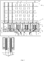
- the first power bus, the second power bus and the plurality of connecting portions define a plurality of first apertures which are arranged in an array, and orthographic projections of the plurality of selector switches on the base substrate fall within the plurality of first apertures.
- the array substrate further includes a third power bus, and an orthographic projection of the third power bus on the base substrate at least partially overlaps with an orthographic projection of the first power bus on the base substrate, and the third power bus is connected to the first power bus.
- an orthographic projection of each of the first gate and the second gate on the base substrate fails to overlap with orthographic projections of the first source, the first drain and the second drain on the base substrate.
- the plurality of data line leads are located in the same layer with the first gate or the second gate.
- the first power bus 08, the second power bus 010 and the plurality of connecting portions 09 define a plurality of first apertures 011 that are arranged in an array, and orthographic projections of the plurality of selector switches 06 on the base substrate 01 fall within the plurality of first apertures 011.
- the plurality of selector switches 06 are in one-to-one correspondence with the plurality of first apertures 011, and the orthographic projection of each selector switch 06 on the base substrate 01 may be located in the corresponding first aperture 011.
- first power bus 08, the second power bus 010 and the connecting portion 09 that are used to transmit the power signal do not overlap with the selector switch 06, thus reducing the parasitic capacitance, and effectively transmitting the power signal to the sub-pixel 02 in the display region AA.
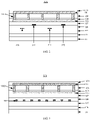
- FIG. 3 is a schematic diagram of a section YY in FIG. 1 provided by an embodiment of the present disclosure.
- the array substrate further includes a fourth power bus 013; an orthographic projection of the fourth power bus 013 on the base substrate 01 at least partially overlaps with an orthographic projection of the second power bus 010 on the base substrate 01; and the fourth power bus 013 is connected to the second power bus 010.
- some insulating layers are provided between the second power bus 010 and the fourth power bus 013, and the second power bus 010 may be connected to the fourth power bus 013 through via holes VH2 in the insulating layers.
- the second power bus 010 may further be connected to the fourth power bus 013, such that the structure used to transmit the power signal is of a double-layer structure, thereby reducing the resistance and the pressure drop when the power signal is transmitted.
- the third power bus 012 in FIG. 2 and the fourth power bus 013 in FIG. 3 may be located in the same layer. With such a manner, when the array substrate is manufactured, the third power bus 012 and the fourth power bus 013 may be manufactured simultaneously, thus reducing the complexity of the process for manufacturing the array substrate. Certainly, the third power bus 012 and the fourth power bus 013 may also not be located in the same layer, which is not limited by the embodiment of the present disclosure thereto.
- the connecting portion 09 of the single-layer structure is used as the example in the embodiment of the present disclosure. Certainly, the connecting portion 09 may also be made into the double-layer structure.
- the connecting portion 09 further includes a connecting sub-portion 09' (not shown and labeled in the drawings of the specification), and the connecting sub-portion 09' is located in the same layer with the third power bus 012, and connected to the third power bus 012 and the fourth power bus 013.
- the connecting portion 09 may further be connected to the connecting sub-portion 09' through a via hole.
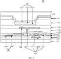
- FIG. 4 is a schematic diagram of a section ZZ in FIG. 1 provided by an embodiment of the present disclosure.
- at least one sub-pixel 02 of the plurality of sub-pixels 02 in the display region AA includes a drive TFT 021 and a connecting electrode 022.
- the drive TFT 021 includes a drive active layer 0211 located on the base substrate 01, a drive gate 0212 located at a side of the drive active layer 0211 away from the base substrate 01, and a drive source 0213 and a drive drain 0214 that are located at a side of the drive gate 0212 away from the base substrate 01.
- the connecting electrode 022 is located at a side of the drive source 0213 and the drive drain 0214 away from the base substrate 01.
- the sub-pixel 02 in FIG. 4 may further include: a buffer layer 024, a first gate insulating layer 025, a second gate insulating layer 026, an interlayer dielectric layer 027, a passivation layer 028, a first planarization layer 029, a second planarization layer 030, a pixel defining layer 031, a support layer 032 and a packaging layer 033 that are sequentially arranged along the direction away from the base substrate 01.
- the buffer layer 024, the first gate insulating layer 025, the second gate insulating layer 026, the interlayer dielectric layer 027, the passivation layer 028, the first planarization layer 029 and the second planarization layer 030 in the display region AA may extend to the peripheral region BB.
- the relative positional relationship among the film layers in the peripheral region BB is the same as that in the display region AA, which is not elaborated herein in the embodiment of the present disclosure.
- the sub-pixel 02 in FIG. 4 may further include: a storage capacitor 034.
- the storage capacitor 034 includes a first capacitive electrode 0341 and a second capacitive electrode 0342.
- the first capacitive electrode 0341 and the drive gate 0212 are located in the same layer, and the second capacitive electrode 0342 is located between the gate insulating layer 026 and the interlayer dielectric layer 027.
- a part of structures of the display region AA and a part of structures of the peripheral region BB in the array substrate may be located in the same layer, and the structures are described hereinafter.
- the first power bus 08 and the second power bus 010 may be located in the same layer with the connecting electrode 022. With such a manner, when the connecting electrode 022 in the display region AA is manufactured, the first power bus 08 and the second power bus 010 in the peripheral region BB may be manufactured simultaneously, thus simplifying the process for manufacturing the array substrate. Certainly, the first power bus 08 and the second power bus 010 may also not be located in the same layer with the connecting electrode 022, which is not limited by the embodiment of the present disclosure thereto.
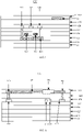
- the first source 064 is connected to one data signal input line 07 of the plurality of data signal input lines 07, and the first drain 065 and the second drain 066 are connected to two data line lead 05 in the plurality of data line leads 05.
- an orthographic projection of each of the first gate 062 and the second gate 063 on the base substrate 01 does not overlap with orthographic projections of the first source 064, the first drain 065 and the second drain 066 on the base substrate 01.
- some structures in the selector switch 06 may be located in the same layer with some structures in the drive transistor.
- the first active layer 061 and the drive active layer 0211 are located in the same layer
- the first gate 062 and the drive gate 0212 are located in the same layer
- the first source 064 and the drive source 0213 are located in the same layer.
- the first active layer 061 and the drive active layer 0211 may also not be located in the same layer
- the first gate 062 and the drive gate 0212 may also not be located in the same layer
- the first source 064 and the drive source 0213 may also not be located in the same layer, which is not limited by the embodiment of the present disclosure thereto.
- the array substrate may further include a first control line 014 and a second control line 015; the first control line 014 is connected to the first gate 062, and the second control line 015 is connected to the second gate 063; and orthographic projections of the first control line 014 and the second control line 015 on the base substrate 01 overlap with the orthographic projections of the plurality of first apertures 011 on the base substrate 01.
- FIG. 6 is a schematic diagram of a section VV in FIG. 1 provided by an embodiment of the present disclosure.
- FIG. 7-1 is a schematic diagram of a section WW in FIG. 1 provided by an embodiment of the present disclosure.
- FIG. 7-2 is a schematic diagram of a section TT in FIG. 1 provided by an embodiment of the present disclosure.
- at least one connecting potion 09 of the plurality of connecting portions 09 includes a second aperture 091, and an orthographic projection of the second aperture 091 on the base substrate 01 overlaps with the orthographic projections of the first control line 014 and the second control line 015 on the base substrate 01.
- the second aperture 091 is provided in the connecting portion 09 in the embodiment of the present disclosure. Under the action of the second aperture 091, the overlapping degree between the connecting portion 09 and the first control line 014 and the second control line 015 can be reduced. Thus, the parasitic capacitance formed by the connecting portion 09 and the two control lines can be reduced, thereby further alleviating the influence on the power signal transmitted on the connecting portion 09.
- the plurality of data signal input lines 07 include a first data signal input line 071 and a second data signal input line 072, the first data signal input line 071 and the second data signal input line 072 are arranged alternately, and the first data signal input line 071 and the second data signal input line 072 are located in different layers.
- the first data signal input line 071 and the drive gate (such as the drive gate 0212 in FIG. 4 ) in the sub-pixel 02 are located in the same layer
- the second data signal input line 072 and the second capacitive electrode 0342 in the sub-pixel 02 are located in the same layer.
- first data signal input line 071 and the drive gate in the sub-pixel 02 may also not be located in the same layer, and the second data signal input line 072 and the second capacitive electrode 0342 in the sub-pixel 02 may also not be located in the same layer, which is not limited by the embodiment of the present disclosure thereto.
- the signal source end in the array substrate may also respectively input the data signal to a plurality of selector switches through a plurality of data signal input lines.
- the signal source end inputs the data signal to one selector switch via each data signal input line
- the data signal is input to the first source of the selector switch.
- the data signal on the first source may be respectively transmitted to two data lines.
- an on signal may be first input to the first control line, such that the first source is connected to the first drain. At this time, the data signal on the first source is transmitted to one data line through the first drain and one data line lead.
- an on signal is input to the second control line, such that the first source is connected to the second drain.
- the data signal on the first source is transmitted to the other data line through the second drain and the other data line lead.
- the sub-pixel connected to each data line also receives the data signal.
- the conductive structure may be made of a transparent material, and may also be made of a nontransparent material, such as a metal simple substance or alloy of indium tin oxide, copper, aluminum, silver, molybdenum, nickel, gold and other metal elements.
- a plurality of sub-pixels, a plurality of data lines, a plurality of first power lines, a plurality of data line leads, a plurality of selector switches, a plurality of data signal input lines, a first power bus and a plurality of connecting portions are formed on a base substrate.
- the base substrate includes a display region and a peripheral region located at at least one side of the display region.
- the plurality of sub-pixels are located in the display region.
- the plurality of data lines are located in the display region, and used to provide data signals for the plurality of sub-pixels.
- the plurality of first power lines are located in the display region, and used to provide a power signal for the plurality of sub-pixels.
- the plurality of data line leads are located in the peripheral region and connected to the plurality of data lines.
- the plurality of selector switches are located in the peripheral region and arranged at intervals, the plurality of selector switches are located at a side of the plurality of data lines away from the display region, and each of at least a part of the plurality of selector switches is connected to at least two data line leads in the plurality of data line leads.
- the plurality of data signal input lines are located in the peripheral region and located at a side of the plurality of selector switches away from the display region, and each of at least a part of the plurality of selector switches is connected to one of the plurality of data signal input lines.
- the plurality of connecting portions are connected to the first power bus and the plurality of first power lines, and the plurality of connecting portions extend towards the display region along regions between the plurality of selector switches.
- one or more of a second power bus, a third power bus, a fourth power bus, a first control line and a second control line may further be manufactured on the base substrate.
- the structures may be referred to the above embodiment of the array substrate, and are not elaborated herein in the embodiment of the present disclosure.
- the method in the embodiment of the present disclosure may be implemented, for example, by the way of changing the pattern on the mask, with reference to any method similar to the method for manufacturing the array substrate provided by the embodiment of the present disclosure, which is not elaborated one by one.
- An embodiment of the present disclosure further provides a display device, including the above any array substrate.
- the display device in the embodiment of the present disclosure may be: any products or parts with display functions, such as a display panel (like the liquid crystal display panel, the OLED display panel and the like), a mobile phone, a tablet computer, a television, a display, a notebook computer, a digital photo frame, a navigator, etc..
- FIG. 8 is a schematic structural diagram of a display device provided by an embodiment of the present disclosure.
- the display device includes the above any display panel, and a display region AA of the display device includes sub-pixels 02 arranged in rows and columns.
- the detailed structure of the peripheral region BB is not shown in FIG. 8 .
- the term "at least one” refers to one or more, and the term "a plurality of' refers to two or more.
- the term "at least one of the followings" or similar expression refers to any combination of these items, including any combination of single items or plural items.
- at least one of a, b or c may be expressed as: a, b, c, a+b, a+c, b+c and a+b+c; and the a, b and c may be the single items, and may also be the plural items.
- the method embodiments according to the embodiments of the present disclosure can be cross-referenced with the embodiments of the corresponding transistor, which is not limited in the embodiments of the present disclosure thereto.
- the sequence of the steps of the method embodiment provided by the embodiments of the present disclosure may be properly adjusted, the steps may also be increased or reduced correspondingly as the case may be, and any method readily conceivable for those skilled in the art within the technical scope disclosed by the present disclosure should be included in the protection scope of the present disclosure and is not elaborated.
Landscapes
- Engineering & Computer Science (AREA)
- Physics & Mathematics (AREA)
- Microelectronics & Electronic Packaging (AREA)
- Computer Hardware Design (AREA)
- General Physics & Mathematics (AREA)
- Theoretical Computer Science (AREA)
- Geometry (AREA)
- Devices For Indicating Variable Information By Combining Individual Elements (AREA)
- Electroluminescent Light Sources (AREA)
Applications Claiming Priority (1)
| Application Number | Priority Date | Filing Date | Title |
|---|---|---|---|
| PCT/CN2019/111057 WO2021072600A1 (zh) | 2019-10-14 | 2019-10-14 | 阵列基板及显示装置 |
Publications (3)
| Publication Number | Publication Date |
|---|---|
| EP4047653A1 true EP4047653A1 (de) | 2022-08-24 |
| EP4047653A4 EP4047653A4 (de) | 2022-11-23 |
| EP4047653B1 EP4047653B1 (de) | 2025-05-07 |
Family
ID=75537301
Family Applications (1)
| Application Number | Title | Priority Date | Filing Date |
|---|---|---|---|
| EP19945474.5A Active EP4047653B1 (de) | 2019-10-14 | 2019-10-14 | Arraysubstrat und anzeigevorrichtung |
Country Status (4)
| Country | Link |
|---|---|
| US (1) | US11551609B2 (de) |
| EP (1) | EP4047653B1 (de) |
| CN (1) | CN115668499B (de) |
| WO (1) | WO2021072600A1 (de) |
Families Citing this family (1)
| Publication number | Priority date | Publication date | Assignee | Title |
|---|---|---|---|---|
| CN115172428B (zh) * | 2022-07-22 | 2025-03-07 | 合肥京东方卓印科技有限公司 | 显示基板及显示装置 |
Family Cites Families (15)
| Publication number | Priority date | Publication date | Assignee | Title |
|---|---|---|---|---|
| JP4165120B2 (ja) * | 2002-05-17 | 2008-10-15 | 株式会社日立製作所 | 画像表示装置 |
| KR100637457B1 (ko) * | 2004-06-29 | 2006-10-20 | 삼성에스디아이 주식회사 | 유기전계 발광 표시 패널 |
| TW200734996A (en) * | 2005-11-29 | 2007-09-16 | Hitachi Displays Ltd | Organic EL display device |
| JP5778485B2 (ja) * | 2011-06-03 | 2015-09-16 | ルネサスエレクトロニクス株式会社 | パネル表示装置のデータドライバ |
| KR102086644B1 (ko) * | 2013-12-31 | 2020-03-09 | 엘지디스플레이 주식회사 | 플렉서블표시장치 및 이의 제조방법 |
| KR102279274B1 (ko) * | 2014-11-05 | 2021-07-21 | 엘지디스플레이 주식회사 | 디지털 엑스레이 검출기용 박막 트랜지스터 어레이 기판 |
| KR102349283B1 (ko) * | 2014-12-19 | 2022-01-11 | 삼성디스플레이 주식회사 | 박막 트랜지스터 어레이 기판, 및 이를 포함하는 유기 발광 표시 장치 |
| CN104900181A (zh) * | 2015-07-03 | 2015-09-09 | 京东方科技集团股份有限公司 | 一种阵列基板及其驱动方法和显示装置 |
| KR102551789B1 (ko) * | 2016-06-15 | 2023-07-07 | 삼성디스플레이 주식회사 | 디스플레이 장치 |
| CN107065336B (zh) * | 2017-06-13 | 2020-05-01 | 厦门天马微电子有限公司 | 一种阵列基板、显示面板及显示装置 |
| KR102555210B1 (ko) * | 2017-12-29 | 2023-07-12 | 엘지디스플레이 주식회사 | 발광 표시 장치 |
| KR102649144B1 (ko) * | 2018-06-25 | 2024-03-21 | 삼성디스플레이 주식회사 | 디스플레이 장치 |
| KR20200028567A (ko) * | 2018-09-06 | 2020-03-17 | 삼성디스플레이 주식회사 | 표시 장치 |
| KR102815241B1 (ko) * | 2019-05-28 | 2025-06-04 | 삼성디스플레이 주식회사 | 표시 장치 |
| CN110148384B (zh) * | 2019-06-28 | 2021-08-03 | 上海天马有机发光显示技术有限公司 | 一种阵列基板、显示面板和像素驱动电路的驱动方法 |
-
2019
- 2019-10-14 EP EP19945474.5A patent/EP4047653B1/de active Active
- 2019-10-14 US US17/256,186 patent/US11551609B2/en active Active
- 2019-10-14 CN CN201980001972.3A patent/CN115668499B/zh active Active
- 2019-10-14 WO PCT/CN2019/111057 patent/WO2021072600A1/zh not_active Ceased
Also Published As
| Publication number | Publication date |
|---|---|
| WO2021072600A1 (zh) | 2021-04-22 |
| EP4047653A4 (de) | 2022-11-23 |
| US11551609B2 (en) | 2023-01-10 |
| CN115668499A (zh) | 2023-01-31 |
| US20210375202A1 (en) | 2021-12-02 |
| EP4047653B1 (de) | 2025-05-07 |
| CN115668499B (zh) | 2025-06-17 |
Similar Documents
| Publication | Publication Date | Title |
|---|---|---|
| EP3565005B1 (de) | Organische lichtemittierende anzeigevorrichtung | |
| US12464910B2 (en) | Display substrate and display device | |
| US10573694B2 (en) | Backplane substrate and flexible display using the same | |
| US10976848B2 (en) | Display apparatus with touch sensor | |
| US11599217B2 (en) | Touch display device | |
| US11387310B2 (en) | Array substrate with connection portion connecting power bus and power line and display panel | |
| CN110797352B (zh) | 显示面板及其制作方法、显示装置 | |
| US11995281B2 (en) | Display device | |
| US20230185400A1 (en) | Touch display device | |
| KR20220149879A (ko) | 표시 장치 | |
| US20260007006A1 (en) | Display device | |
| US20240324333A1 (en) | Display Substrate and Preparation Method therefor, and Display Apparatus | |
| EP4047653B1 (de) | Arraysubstrat und anzeigevorrichtung | |
| US20220335883A1 (en) | Display device and manufacturing method of the same | |
| US20250056890A1 (en) | Display panels including metal layer having fan-out segment and display terminals including the same | |
| US11024697B2 (en) | Display apparatus and method of manufacturing the same | |
| KR102911310B1 (ko) | 유기 발광 표시 장치 | |
| US12282618B2 (en) | Display apparatus | |
| US20260044226A1 (en) | Display apparatus | |
| US12414419B2 (en) | Display substrate | |
| JP7753325B2 (ja) | 発光表示装置 | |
| CN113628577B (zh) | 一种显示基板、显示面板和显示装置 | |
| KR20250135936A (ko) | 표시 장치 | |
| EP4080576A1 (de) | Anzeigevorrichtung, anzeigetafel und herstellungsverfahren dafür | |
| CN119173810A (zh) | 显示基板及其制备方法和显示装置 |
Legal Events
| Date | Code | Title | Description |
|---|---|---|---|
| STAA | Information on the status of an ep patent application or granted ep patent |
Free format text: STATUS: UNKNOWN |
|
| STAA | Information on the status of an ep patent application or granted ep patent |
Free format text: STATUS: THE INTERNATIONAL PUBLICATION HAS BEEN MADE |
|
| PUAI | Public reference made under article 153(3) epc to a published international application that has entered the european phase |
Free format text: ORIGINAL CODE: 0009012 |
|
| STAA | Information on the status of an ep patent application or granted ep patent |
Free format text: STATUS: REQUEST FOR EXAMINATION WAS MADE |
|
| 17P | Request for examination filed |
Effective date: 20210326 |
|
| AK | Designated contracting states |
Kind code of ref document: A1 Designated state(s): AL AT BE BG CH CY CZ DE DK EE ES FI FR GB GR HR HU IE IS IT LI LT LU LV MC MK MT NL NO PL PT RO RS SE SI SK SM TR |
|
| A4 | Supplementary search report drawn up and despatched |
Effective date: 20221026 |
|
| RIC1 | Information provided on ipc code assigned before grant |
Ipc: G09G 3/3225 20160101ALI20221020BHEP Ipc: H01L 27/12 20060101AFI20221020BHEP |
|
| DAV | Request for validation of the european patent (deleted) | ||
| DAX | Request for extension of the european patent (deleted) | ||
| GRAP | Despatch of communication of intention to grant a patent |
Free format text: ORIGINAL CODE: EPIDOSNIGR1 |
|
| STAA | Information on the status of an ep patent application or granted ep patent |
Free format text: STATUS: GRANT OF PATENT IS INTENDED |
|
| INTG | Intention to grant announced |
Effective date: 20241206 |
|
| GRAS | Grant fee paid |
Free format text: ORIGINAL CODE: EPIDOSNIGR3 |
|
| GRAA | (expected) grant |
Free format text: ORIGINAL CODE: 0009210 |
|
| STAA | Information on the status of an ep patent application or granted ep patent |
Free format text: STATUS: THE PATENT HAS BEEN GRANTED |
|
| AK | Designated contracting states |
Kind code of ref document: B1 Designated state(s): AL AT BE BG CH CY CZ DE DK EE ES FI FR GB GR HR HU IE IS IT LI LT LU LV MC MK MT NL NO PL PT RO RS SE SI SK SM TR |
|
| REG | Reference to a national code |
Ref country code: GB Ref legal event code: FG4D |
|
| REG | Reference to a national code |
Ref country code: DE Ref legal event code: R096 Ref document number: 602019069829 Country of ref document: DE |
|
| REG | Reference to a national code |
Ref country code: IE Ref legal event code: FG4D |
|
| REG | Reference to a national code |
Ref country code: NL Ref legal event code: MP Effective date: 20250507 |
|
| PG25 | Lapsed in a contracting state [announced via postgrant information from national office to epo] |
Ref country code: FI Free format text: LAPSE BECAUSE OF FAILURE TO SUBMIT A TRANSLATION OF THE DESCRIPTION OR TO PAY THE FEE WITHIN THE PRESCRIBED TIME-LIMIT Effective date: 20250507 Ref country code: ES Free format text: LAPSE BECAUSE OF FAILURE TO SUBMIT A TRANSLATION OF THE DESCRIPTION OR TO PAY THE FEE WITHIN THE PRESCRIBED TIME-LIMIT Effective date: 20250507 Ref country code: PT Free format text: LAPSE BECAUSE OF FAILURE TO SUBMIT A TRANSLATION OF THE DESCRIPTION OR TO PAY THE FEE WITHIN THE PRESCRIBED TIME-LIMIT Effective date: 20250908 |
|
| REG | Reference to a national code |
Ref country code: LT Ref legal event code: MG9D |
|
| PG25 | Lapsed in a contracting state [announced via postgrant information from national office to epo] |
Ref country code: NO Free format text: LAPSE BECAUSE OF FAILURE TO SUBMIT A TRANSLATION OF THE DESCRIPTION OR TO PAY THE FEE WITHIN THE PRESCRIBED TIME-LIMIT Effective date: 20250807 Ref country code: GR Free format text: LAPSE BECAUSE OF FAILURE TO SUBMIT A TRANSLATION OF THE DESCRIPTION OR TO PAY THE FEE WITHIN THE PRESCRIBED TIME-LIMIT Effective date: 20250808 |
|
| PG25 | Lapsed in a contracting state [announced via postgrant information from national office to epo] |
Ref country code: PL Free format text: LAPSE BECAUSE OF FAILURE TO SUBMIT A TRANSLATION OF THE DESCRIPTION OR TO PAY THE FEE WITHIN THE PRESCRIBED TIME-LIMIT Effective date: 20250507 Ref country code: NL Free format text: LAPSE BECAUSE OF FAILURE TO SUBMIT A TRANSLATION OF THE DESCRIPTION OR TO PAY THE FEE WITHIN THE PRESCRIBED TIME-LIMIT Effective date: 20250507 |
|
| REG | Reference to a national code |
Ref country code: AT Ref legal event code: MK05 Ref document number: 1793475 Country of ref document: AT Kind code of ref document: T Effective date: 20250507 |
|
| PG25 | Lapsed in a contracting state [announced via postgrant information from national office to epo] |
Ref country code: BG Free format text: LAPSE BECAUSE OF FAILURE TO SUBMIT A TRANSLATION OF THE DESCRIPTION OR TO PAY THE FEE WITHIN THE PRESCRIBED TIME-LIMIT Effective date: 20250507 |
|
| PG25 | Lapsed in a contracting state [announced via postgrant information from national office to epo] |
Ref country code: HR Free format text: LAPSE BECAUSE OF FAILURE TO SUBMIT A TRANSLATION OF THE DESCRIPTION OR TO PAY THE FEE WITHIN THE PRESCRIBED TIME-LIMIT Effective date: 20250507 |
|
| PG25 | Lapsed in a contracting state [announced via postgrant information from national office to epo] |
Ref country code: AT Free format text: LAPSE BECAUSE OF FAILURE TO SUBMIT A TRANSLATION OF THE DESCRIPTION OR TO PAY THE FEE WITHIN THE PRESCRIBED TIME-LIMIT Effective date: 20250507 |
|
| PG25 | Lapsed in a contracting state [announced via postgrant information from national office to epo] |
Ref country code: RS Free format text: LAPSE BECAUSE OF FAILURE TO SUBMIT A TRANSLATION OF THE DESCRIPTION OR TO PAY THE FEE WITHIN THE PRESCRIBED TIME-LIMIT Effective date: 20250807 |
|
| PG25 | Lapsed in a contracting state [announced via postgrant information from national office to epo] |
Ref country code: IS Free format text: LAPSE BECAUSE OF FAILURE TO SUBMIT A TRANSLATION OF THE DESCRIPTION OR TO PAY THE FEE WITHIN THE PRESCRIBED TIME-LIMIT Effective date: 20250907 |
|
| PG25 | Lapsed in a contracting state [announced via postgrant information from national office to epo] |
Ref country code: LV Free format text: LAPSE BECAUSE OF FAILURE TO SUBMIT A TRANSLATION OF THE DESCRIPTION OR TO PAY THE FEE WITHIN THE PRESCRIBED TIME-LIMIT Effective date: 20250507 |
|
| PGFP | Annual fee paid to national office [announced via postgrant information from national office to epo] |
Ref country code: DE Payment date: 20251021 Year of fee payment: 7 |
|
| PGFP | Annual fee paid to national office [announced via postgrant information from national office to epo] |
Ref country code: GB Payment date: 20251022 Year of fee payment: 7 |
|
| PG25 | Lapsed in a contracting state [announced via postgrant information from national office to epo] |
Ref country code: DK Free format text: LAPSE BECAUSE OF FAILURE TO SUBMIT A TRANSLATION OF THE DESCRIPTION OR TO PAY THE FEE WITHIN THE PRESCRIBED TIME-LIMIT Effective date: 20250507 Ref country code: SM Free format text: LAPSE BECAUSE OF FAILURE TO SUBMIT A TRANSLATION OF THE DESCRIPTION OR TO PAY THE FEE WITHIN THE PRESCRIBED TIME-LIMIT Effective date: 20250507 |
|
| PG25 | Lapsed in a contracting state [announced via postgrant information from national office to epo] |
Ref country code: CZ Free format text: LAPSE BECAUSE OF FAILURE TO SUBMIT A TRANSLATION OF THE DESCRIPTION OR TO PAY THE FEE WITHIN THE PRESCRIBED TIME-LIMIT Effective date: 20250507 |
|
| PG25 | Lapsed in a contracting state [announced via postgrant information from national office to epo] |
Ref country code: EE Free format text: LAPSE BECAUSE OF FAILURE TO SUBMIT A TRANSLATION OF THE DESCRIPTION OR TO PAY THE FEE WITHIN THE PRESCRIBED TIME-LIMIT Effective date: 20250507 |
|
| PG25 | Lapsed in a contracting state [announced via postgrant information from national office to epo] |
Ref country code: SK Free format text: LAPSE BECAUSE OF FAILURE TO SUBMIT A TRANSLATION OF THE DESCRIPTION OR TO PAY THE FEE WITHIN THE PRESCRIBED TIME-LIMIT Effective date: 20250507 |
|
| PG25 | Lapsed in a contracting state [announced via postgrant information from national office to epo] |
Ref country code: IT Free format text: LAPSE BECAUSE OF FAILURE TO SUBMIT A TRANSLATION OF THE DESCRIPTION OR TO PAY THE FEE WITHIN THE PRESCRIBED TIME-LIMIT Effective date: 20250507 |