EP4047650A1 - Semiconductor package - Google Patents
Semiconductor package Download PDFInfo
- Publication number
- EP4047650A1 EP4047650A1 EP22158074.9A EP22158074A EP4047650A1 EP 4047650 A1 EP4047650 A1 EP 4047650A1 EP 22158074 A EP22158074 A EP 22158074A EP 4047650 A1 EP4047650 A1 EP 4047650A1
- Authority
- EP
- European Patent Office
- Prior art keywords
- package
- carrier
- electronic element
- electrical surface
- semiconductor package
- Prior art date
- Legal status (The legal status is an assumption and is not a legal conclusion. Google has not performed a legal analysis and makes no representation as to the accuracy of the status listed.)
- Withdrawn
Links
Images



Classifications
-
- H—ELECTRICITY
- H10—SEMICONDUCTOR DEVICES; ELECTRIC SOLID-STATE DEVICES NOT OTHERWISE PROVIDED FOR
- H10W—GENERIC PACKAGES, INTERCONNECTIONS, CONNECTORS OR OTHER CONSTRUCTIONAL DETAILS OF DEVICES COVERED BY CLASS H10
- H10W74/00—Encapsulations, e.g. protective coatings
- H10W74/10—Encapsulations, e.g. protective coatings characterised by their shape or disposition
- H10W74/111—Encapsulations, e.g. protective coatings characterised by their shape or disposition the semiconductor body being completely enclosed
- H10W74/114—Encapsulations, e.g. protective coatings characterised by their shape or disposition the semiconductor body being completely enclosed by a substrate and the encapsulations
-
- H—ELECTRICITY
- H10—SEMICONDUCTOR DEVICES; ELECTRIC SOLID-STATE DEVICES NOT OTHERWISE PROVIDED FOR
- H10W—GENERIC PACKAGES, INTERCONNECTIONS, CONNECTORS OR OTHER CONSTRUCTIONAL DETAILS OF DEVICES COVERED BY CLASS H10
- H10W70/00—Package substrates; Interposers; Redistribution layers [RDL]
- H10W70/40—Leadframes
- H10W70/479—Leadframes on or in insulating or insulated package substrates, interposers, or redistribution layers
-
- H—ELECTRICITY
- H10—SEMICONDUCTOR DEVICES; ELECTRIC SOLID-STATE DEVICES NOT OTHERWISE PROVIDED FOR
- H10W—GENERIC PACKAGES, INTERCONNECTIONS, CONNECTORS OR OTHER CONSTRUCTIONAL DETAILS OF DEVICES COVERED BY CLASS H10
- H10W20/00—Interconnections in chips, wafers or substrates
- H10W20/40—Interconnections external to wafers or substrates, e.g. back-end-of-line [BEOL] metallisations or vias connecting to gate electrodes
-
- H—ELECTRICITY
- H10—SEMICONDUCTOR DEVICES; ELECTRIC SOLID-STATE DEVICES NOT OTHERWISE PROVIDED FOR
- H10W—GENERIC PACKAGES, INTERCONNECTIONS, CONNECTORS OR OTHER CONSTRUCTIONAL DETAILS OF DEVICES COVERED BY CLASS H10
- H10W20/00—Interconnections in chips, wafers or substrates
- H10W20/40—Interconnections external to wafers or substrates, e.g. back-end-of-line [BEOL] metallisations or vias connecting to gate electrodes
- H10W20/482—Interconnections external to wafers or substrates, e.g. back-end-of-line [BEOL] metallisations or vias connecting to gate electrodes for individual devices provided for in groups H10D8/00 - H10D48/00, e.g. for power transistors
- H10W20/484—Interconnections having extended contours, e.g. pads having mesh shape or interconnections comprising connected parallel stripes
-
- H—ELECTRICITY
- H10—SEMICONDUCTOR DEVICES; ELECTRIC SOLID-STATE DEVICES NOT OTHERWISE PROVIDED FOR
- H10W—GENERIC PACKAGES, INTERCONNECTIONS, CONNECTORS OR OTHER CONSTRUCTIONAL DETAILS OF DEVICES COVERED BY CLASS H10
- H10W70/00—Package substrates; Interposers; Redistribution layers [RDL]
- H10W70/40—Leadframes
- H10W70/464—Additional interconnections in combination with leadframes
- H10W70/468—Circuit boards
-
- H—ELECTRICITY
- H10—SEMICONDUCTOR DEVICES; ELECTRIC SOLID-STATE DEVICES NOT OTHERWISE PROVIDED FOR
- H10W—GENERIC PACKAGES, INTERCONNECTIONS, CONNECTORS OR OTHER CONSTRUCTIONAL DETAILS OF DEVICES COVERED BY CLASS H10
- H10W70/00—Package substrates; Interposers; Redistribution layers [RDL]
- H10W70/60—Insulating or insulated package substrates; Interposers; Redistribution layers
- H10W70/62—Insulating or insulated package substrates; Interposers; Redistribution layers characterised by their interconnections
- H10W70/63—Vias, e.g. via plugs
- H10W70/635—Through-vias
-
- H—ELECTRICITY
- H10—SEMICONDUCTOR DEVICES; ELECTRIC SOLID-STATE DEVICES NOT OTHERWISE PROVIDED FOR
- H10W—GENERIC PACKAGES, INTERCONNECTIONS, CONNECTORS OR OTHER CONSTRUCTIONAL DETAILS OF DEVICES COVERED BY CLASS H10
- H10W70/00—Package substrates; Interposers; Redistribution layers [RDL]
- H10W70/60—Insulating or insulated package substrates; Interposers; Redistribution layers
- H10W70/67—Insulating or insulated package substrates; Interposers; Redistribution layers characterised by their insulating layers or insulating parts
- H10W70/68—Shapes or dispositions thereof
-
- H—ELECTRICITY
- H10—SEMICONDUCTOR DEVICES; ELECTRIC SOLID-STATE DEVICES NOT OTHERWISE PROVIDED FOR
- H10W—GENERIC PACKAGES, INTERCONNECTIONS, CONNECTORS OR OTHER CONSTRUCTIONAL DETAILS OF DEVICES COVERED BY CLASS H10
- H10W90/00—Package configurations
-
- H—ELECTRICITY
- H10—SEMICONDUCTOR DEVICES; ELECTRIC SOLID-STATE DEVICES NOT OTHERWISE PROVIDED FOR
- H10W—GENERIC PACKAGES, INTERCONNECTIONS, CONNECTORS OR OTHER CONSTRUCTIONAL DETAILS OF DEVICES COVERED BY CLASS H10
- H10W90/00—Package configurations
- H10W90/811—Multiple chips on leadframes
-
- H—ELECTRICITY
- H10—SEMICONDUCTOR DEVICES; ELECTRIC SOLID-STATE DEVICES NOT OTHERWISE PROVIDED FOR
- H10W—GENERIC PACKAGES, INTERCONNECTIONS, CONNECTORS OR OTHER CONSTRUCTIONAL DETAILS OF DEVICES COVERED BY CLASS H10
- H10W72/00—Interconnections or connectors in packages
- H10W72/071—Connecting or disconnecting
- H10W72/073—Connecting or disconnecting of die-attach connectors
-
- H—ELECTRICITY
- H10—SEMICONDUCTOR DEVICES; ELECTRIC SOLID-STATE DEVICES NOT OTHERWISE PROVIDED FOR
- H10W—GENERIC PACKAGES, INTERCONNECTIONS, CONNECTORS OR OTHER CONSTRUCTIONAL DETAILS OF DEVICES COVERED BY CLASS H10
- H10W72/00—Interconnections or connectors in packages
- H10W72/071—Connecting or disconnecting
- H10W72/075—Connecting or disconnecting of bond wires
- H10W72/07551—Connecting or disconnecting of bond wires characterised by changes in properties of the bond wires during the connecting
- H10W72/07554—Connecting or disconnecting of bond wires characterised by changes in properties of the bond wires during the connecting changes in dispositions
-
- H—ELECTRICITY
- H10—SEMICONDUCTOR DEVICES; ELECTRIC SOLID-STATE DEVICES NOT OTHERWISE PROVIDED FOR
- H10W—GENERIC PACKAGES, INTERCONNECTIONS, CONNECTORS OR OTHER CONSTRUCTIONAL DETAILS OF DEVICES COVERED BY CLASS H10
- H10W72/00—Interconnections or connectors in packages
- H10W72/30—Die-attach connectors
- H10W72/341—Dispositions of die-attach connectors, e.g. layouts
-
- H—ELECTRICITY
- H10—SEMICONDUCTOR DEVICES; ELECTRIC SOLID-STATE DEVICES NOT OTHERWISE PROVIDED FOR
- H10W—GENERIC PACKAGES, INTERCONNECTIONS, CONNECTORS OR OTHER CONSTRUCTIONAL DETAILS OF DEVICES COVERED BY CLASS H10
- H10W72/00—Interconnections or connectors in packages
- H10W72/50—Bond wires
-
- H—ELECTRICITY
- H10—SEMICONDUCTOR DEVICES; ELECTRIC SOLID-STATE DEVICES NOT OTHERWISE PROVIDED FOR
- H10W—GENERIC PACKAGES, INTERCONNECTIONS, CONNECTORS OR OTHER CONSTRUCTIONAL DETAILS OF DEVICES COVERED BY CLASS H10
- H10W72/00—Interconnections or connectors in packages
- H10W72/50—Bond wires
- H10W72/541—Dispositions of bond wires
- H10W72/547—Dispositions of multiple bond wires
-
- H—ELECTRICITY
- H10—SEMICONDUCTOR DEVICES; ELECTRIC SOLID-STATE DEVICES NOT OTHERWISE PROVIDED FOR
- H10W—GENERIC PACKAGES, INTERCONNECTIONS, CONNECTORS OR OTHER CONSTRUCTIONAL DETAILS OF DEVICES COVERED BY CLASS H10
- H10W72/00—Interconnections or connectors in packages
- H10W72/50—Bond wires
- H10W72/551—Materials of bond wires
-
- H—ELECTRICITY
- H10—SEMICONDUCTOR DEVICES; ELECTRIC SOLID-STATE DEVICES NOT OTHERWISE PROVIDED FOR
- H10W—GENERIC PACKAGES, INTERCONNECTIONS, CONNECTORS OR OTHER CONSTRUCTIONAL DETAILS OF DEVICES COVERED BY CLASS H10
- H10W72/00—Interconnections or connectors in packages
- H10W72/50—Bond wires
- H10W72/551—Materials of bond wires
- H10W72/552—Materials of bond wires comprising metals or metalloids, e.g. silver
-
- H—ELECTRICITY
- H10—SEMICONDUCTOR DEVICES; ELECTRIC SOLID-STATE DEVICES NOT OTHERWISE PROVIDED FOR
- H10W—GENERIC PACKAGES, INTERCONNECTIONS, CONNECTORS OR OTHER CONSTRUCTIONAL DETAILS OF DEVICES COVERED BY CLASS H10
- H10W72/00—Interconnections or connectors in packages
- H10W72/50—Bond wires
- H10W72/551—Materials of bond wires
- H10W72/552—Materials of bond wires comprising metals or metalloids, e.g. silver
- H10W72/5522—Materials of bond wires comprising metals or metalloids, e.g. silver comprising gold [Au]
-
- H—ELECTRICITY
- H10—SEMICONDUCTOR DEVICES; ELECTRIC SOLID-STATE DEVICES NOT OTHERWISE PROVIDED FOR
- H10W—GENERIC PACKAGES, INTERCONNECTIONS, CONNECTORS OR OTHER CONSTRUCTIONAL DETAILS OF DEVICES COVERED BY CLASS H10
- H10W72/00—Interconnections or connectors in packages
- H10W72/50—Bond wires
- H10W72/551—Materials of bond wires
- H10W72/552—Materials of bond wires comprising metals or metalloids, e.g. silver
- H10W72/5525—Materials of bond wires comprising metals or metalloids, e.g. silver comprising copper [Cu]
-
- H—ELECTRICITY
- H10—SEMICONDUCTOR DEVICES; ELECTRIC SOLID-STATE DEVICES NOT OTHERWISE PROVIDED FOR
- H10W—GENERIC PACKAGES, INTERCONNECTIONS, CONNECTORS OR OTHER CONSTRUCTIONAL DETAILS OF DEVICES COVERED BY CLASS H10
- H10W72/00—Interconnections or connectors in packages
- H10W72/851—Dispositions of multiple connectors or interconnections
- H10W72/853—On the same surface
- H10W72/865—Die-attach connectors and bond wires
-
- H—ELECTRICITY
- H10—SEMICONDUCTOR DEVICES; ELECTRIC SOLID-STATE DEVICES NOT OTHERWISE PROVIDED FOR
- H10W—GENERIC PACKAGES, INTERCONNECTIONS, CONNECTORS OR OTHER CONSTRUCTIONAL DETAILS OF DEVICES COVERED BY CLASS H10
- H10W72/00—Interconnections or connectors in packages
- H10W72/851—Dispositions of multiple connectors or interconnections
- H10W72/874—On different surfaces
- H10W72/884—Die-attach connectors and bond wires
-
- H—ELECTRICITY
- H10—SEMICONDUCTOR DEVICES; ELECTRIC SOLID-STATE DEVICES NOT OTHERWISE PROVIDED FOR
- H10W—GENERIC PACKAGES, INTERCONNECTIONS, CONNECTORS OR OTHER CONSTRUCTIONAL DETAILS OF DEVICES COVERED BY CLASS H10
- H10W72/00—Interconnections or connectors in packages
- H10W72/90—Bond pads, in general
- H10W72/931—Shapes of bond pads
- H10W72/932—Plan-view shape, i.e. in top view
-
- H—ELECTRICITY
- H10—SEMICONDUCTOR DEVICES; ELECTRIC SOLID-STATE DEVICES NOT OTHERWISE PROVIDED FOR
- H10W—GENERIC PACKAGES, INTERCONNECTIONS, CONNECTORS OR OTHER CONSTRUCTIONAL DETAILS OF DEVICES COVERED BY CLASS H10
- H10W72/00—Interconnections or connectors in packages
- H10W72/90—Bond pads, in general
- H10W72/941—Dispositions of bond pads
- H10W72/944—Dispositions of multiple bond pads
- H10W72/9445—Top-view layouts, e.g. mirror arrays
-
- H—ELECTRICITY
- H10—SEMICONDUCTOR DEVICES; ELECTRIC SOLID-STATE DEVICES NOT OTHERWISE PROVIDED FOR
- H10W—GENERIC PACKAGES, INTERCONNECTIONS, CONNECTORS OR OTHER CONSTRUCTIONAL DETAILS OF DEVICES COVERED BY CLASS H10
- H10W74/00—Encapsulations, e.g. protective coatings
-
- H—ELECTRICITY
- H10—SEMICONDUCTOR DEVICES; ELECTRIC SOLID-STATE DEVICES NOT OTHERWISE PROVIDED FOR
- H10W—GENERIC PACKAGES, INTERCONNECTIONS, CONNECTORS OR OTHER CONSTRUCTIONAL DETAILS OF DEVICES COVERED BY CLASS H10
- H10W74/00—Encapsulations, e.g. protective coatings
- H10W74/10—Encapsulations, e.g. protective coatings characterised by their shape or disposition
- H10W74/111—Encapsulations, e.g. protective coatings characterised by their shape or disposition the semiconductor body being completely enclosed
- H10W74/121—Encapsulations, e.g. protective coatings characterised by their shape or disposition the semiconductor body being completely enclosed by multiple encapsulations, e.g. by a thin protective coating and a thick encapsulation
-
- H—ELECTRICITY
- H10—SEMICONDUCTOR DEVICES; ELECTRIC SOLID-STATE DEVICES NOT OTHERWISE PROVIDED FOR
- H10W—GENERIC PACKAGES, INTERCONNECTIONS, CONNECTORS OR OTHER CONSTRUCTIONAL DETAILS OF DEVICES COVERED BY CLASS H10
- H10W90/00—Package configurations
- H10W90/20—Configurations of stacked chips
- H10W90/24—Configurations of stacked chips at least one of the stacked chips being laterally offset from a neighbouring stacked chip, e.g. chip stacks having a staircase shape
-
- H—ELECTRICITY
- H10—SEMICONDUCTOR DEVICES; ELECTRIC SOLID-STATE DEVICES NOT OTHERWISE PROVIDED FOR
- H10W—GENERIC PACKAGES, INTERCONNECTIONS, CONNECTORS OR OTHER CONSTRUCTIONAL DETAILS OF DEVICES COVERED BY CLASS H10
- H10W90/00—Package configurations
- H10W90/701—Package configurations characterised by the relative positions of pads or connectors relative to package parts
- H10W90/731—Package configurations characterised by the relative positions of pads or connectors relative to package parts of die-attach connectors
- H10W90/732—Package configurations characterised by the relative positions of pads or connectors relative to package parts of die-attach connectors between stacked chips
-
- H—ELECTRICITY
- H10—SEMICONDUCTOR DEVICES; ELECTRIC SOLID-STATE DEVICES NOT OTHERWISE PROVIDED FOR
- H10W—GENERIC PACKAGES, INTERCONNECTIONS, CONNECTORS OR OTHER CONSTRUCTIONAL DETAILS OF DEVICES COVERED BY CLASS H10
- H10W90/00—Package configurations
- H10W90/701—Package configurations characterised by the relative positions of pads or connectors relative to package parts
- H10W90/731—Package configurations characterised by the relative positions of pads or connectors relative to package parts of die-attach connectors
- H10W90/734—Package configurations characterised by the relative positions of pads or connectors relative to package parts of die-attach connectors between a chip and a stacked insulating package substrate, interposer or RDL
-
- H—ELECTRICITY
- H10—SEMICONDUCTOR DEVICES; ELECTRIC SOLID-STATE DEVICES NOT OTHERWISE PROVIDED FOR
- H10W—GENERIC PACKAGES, INTERCONNECTIONS, CONNECTORS OR OTHER CONSTRUCTIONAL DETAILS OF DEVICES COVERED BY CLASS H10
- H10W90/00—Package configurations
- H10W90/701—Package configurations characterised by the relative positions of pads or connectors relative to package parts
- H10W90/731—Package configurations characterised by the relative positions of pads or connectors relative to package parts of die-attach connectors
- H10W90/736—Package configurations characterised by the relative positions of pads or connectors relative to package parts of die-attach connectors between a chip and a stacked lead frame, conducting package substrate or heat sink
-
- H—ELECTRICITY
- H10—SEMICONDUCTOR DEVICES; ELECTRIC SOLID-STATE DEVICES NOT OTHERWISE PROVIDED FOR
- H10W—GENERIC PACKAGES, INTERCONNECTIONS, CONNECTORS OR OTHER CONSTRUCTIONAL DETAILS OF DEVICES COVERED BY CLASS H10
- H10W90/00—Package configurations
- H10W90/701—Package configurations characterised by the relative positions of pads or connectors relative to package parts
- H10W90/751—Package configurations characterised by the relative positions of pads or connectors relative to package parts of bond wires
- H10W90/752—Package configurations characterised by the relative positions of pads or connectors relative to package parts of bond wires between stacked chips
-
- H—ELECTRICITY
- H10—SEMICONDUCTOR DEVICES; ELECTRIC SOLID-STATE DEVICES NOT OTHERWISE PROVIDED FOR
- H10W—GENERIC PACKAGES, INTERCONNECTIONS, CONNECTORS OR OTHER CONSTRUCTIONAL DETAILS OF DEVICES COVERED BY CLASS H10
- H10W90/00—Package configurations
- H10W90/701—Package configurations characterised by the relative positions of pads or connectors relative to package parts
- H10W90/751—Package configurations characterised by the relative positions of pads or connectors relative to package parts of bond wires
- H10W90/753—Package configurations characterised by the relative positions of pads or connectors relative to package parts of bond wires between laterally-adjacent chips
-
- H—ELECTRICITY
- H10—SEMICONDUCTOR DEVICES; ELECTRIC SOLID-STATE DEVICES NOT OTHERWISE PROVIDED FOR
- H10W—GENERIC PACKAGES, INTERCONNECTIONS, CONNECTORS OR OTHER CONSTRUCTIONAL DETAILS OF DEVICES COVERED BY CLASS H10
- H10W90/00—Package configurations
- H10W90/701—Package configurations characterised by the relative positions of pads or connectors relative to package parts
- H10W90/751—Package configurations characterised by the relative positions of pads or connectors relative to package parts of bond wires
- H10W90/754—Package configurations characterised by the relative positions of pads or connectors relative to package parts of bond wires between a chip and a stacked insulating package substrate, interposer or RDL
-
- H—ELECTRICITY
- H10—SEMICONDUCTOR DEVICES; ELECTRIC SOLID-STATE DEVICES NOT OTHERWISE PROVIDED FOR
- H10W—GENERIC PACKAGES, INTERCONNECTIONS, CONNECTORS OR OTHER CONSTRUCTIONAL DETAILS OF DEVICES COVERED BY CLASS H10
- H10W90/00—Package configurations
- H10W90/701—Package configurations characterised by the relative positions of pads or connectors relative to package parts
- H10W90/751—Package configurations characterised by the relative positions of pads or connectors relative to package parts of bond wires
- H10W90/756—Package configurations characterised by the relative positions of pads or connectors relative to package parts of bond wires between a chip and a stacked lead frame, conducting package substrate or heat sink
Definitions
- the invention relates to a semiconductor package, and more particularly to a semiconductor package including a package module.
- Conventional semiconductor package includes a lead frame, a chip and a plurality of solder wires.
- the chip is disposed on the lead frame, and the solder wires electrically connect the chip with the lead frame.
- the conductive wires are boned to the lead frame which is thin, and thus it cause unreliability of bonding. Thus, how to bond the conductive wire in a way of reliability has become a prominent task for the industries.
- a semiconductor package in an embodiment of the invention, includes a carrier, a package module and a second package body.
- the package module is disposed on the carrier and includes a first substrate, a first electronic element, a first conductive wire and a first package body.
- the first substrate has a first electrical surface facing the carrier and a second electrical surface opposite to the first electrical surface.
- the first electronic element is disposed on the first electrical surface.
- the first conductive wire connects the electronic element with the first electrical surface of the first substrate.
- the first package body encapsulates the first electrical surface, the first electronic element and the first solder wire.
- the second package body encapsulates the package module and a portion of the carrier.
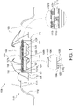
- FIG. 1 illustrates a diagram view of a semiconductor package 100 according to an embodiment of the invention
- FIGS. 2 and 3 illustrate top views of configuration relationships between the package module 120 and the second electronic element 150 of FIG. 1 .
- the semiconductor package 100 includes a carrier 110, a package module 120, a first adhesive layer 125, a second package body 130, at least one second conductive wire140, at least one second electronic element 150, a second adhesive layer 155 and at least one third electronic element 160.
- the conductive wire could be made of a material including, for example, Au, Ag, Cu, Ni, etc.
- the package module 120 is disposed on the carrier 110 and includes a first substrate 121, at least one first electronic element 122, at least one first conductive wire 123 and a first package body 124.
- the first substrate 121 has a first electrical surface 121b facing the carrier 110 and a second electrical surface 121u opposite to the first electrical surface 121b.
- the first electronic elements 122 are disposed on the first electrical surface 121b.
- the first conductive wires 123 connect the first electronic elements 122 with the first electrical surface 121b of the first substrate 121.
- the first package body 124 encapsulates the first electrical surface 121b, the first electronic element 122 and the first conductive wires 123.
- the second package body 130 encapsulates the package module 120 and a portion of the carrier 110.
- the conductive wire could more reliably (or steadily) be boned to the package module 120.
- the package module 120 provides a steady platform, it could increase the stability of the wire bonding and reduce the complexity of the wire bonding.
- the electronic elements 122 being embedded in the first package body 124 in advance, the required number of the second conductive wires 140 could be reduced and/or it could reduce the complexity of the wire bonding.
- the carrier 110 is, for example, lead frame.
- the carrier 110 includes a plurality of inner leads 111, a plurality of outer leads 112, a grounding ring 113 and a die pad 114, wherein each the outer lead 112 is connected to the corresponding inner lead 111, and the grounding ring 113 could be connected to one or some of the inner leads 111.
- the inner leads 111 and the grounding ring 113 are encapsulated by the second package body 130, and the outer leads 112 protrude relative to the second package body 130 for electrically connected with an external electronic device.
- PCB Printed Circuit Board
- the die pad 114 could carry the package module 120.
- the package module 120 further has a package surface 120b away from the second electrical surface 121u.
- the package surface 120b faces the carrier 110, and the second electrical surface 121u faces away from the carrier 110.
- the first substrate 121 has, for example, single-layered structure or multi-layered structure.
- the first substrate 121 has multi-layered structure including at least one dielectric layer 1211, at least one conductive layer 1212 and at least one conductive via 1213.
- the dielectric layer 1211 could be made of a material of non-conductive material, for example, epoxy or resin.
- Two of the conductive layers 1212 are separated from each other by one of the dielectric layers 1211, and electrically connected with each other by one of the conductive vias 1213.
- Each conductive layer 1212 includes at least one trace, and at least one conductive via 1213 connects with the traces of the conductive layers 1212.
- the bottommost conductive layer 1212 includes at least one trace and/or pad which form the first electrical surface 121b, and the bottommost conductive layer 1212 could be covered by solder mask (not illustrated) exposing the pad.
- the topmost dielectric layer 1212 includes at least one trace and/or pad which form the second electrical surface 121u, and the topmost conductive layer 1212 could be covered by solder mask (not illustrated) exposing the pad.
- the first substrate 121 is, for example, a PCB, interposer, etc.; however, such exemplification is not meant to be for limiting.
- first electronic elements 122 could be stacked each other and/or a group of the stacked first electronic elements 122 and another group of the stacked first electronic elements 122 are disposed side by side.
- the number of a group of the stacked first electronic elements 122 is, for example, two, three or more.
- the number of the stacked group including the stacked first electronic elements 122 is, for example, one, two, three or more.
- two first electronic elements 122 on which no first electronic element 122 is stacked are disposed with side by side, or one first electronic element 122 on which no first electronic element 122 is stacked and one stacked group of are disposed with side by side.
- the first electronic element 122 is, for example, memory chip, Sop (System on a Chip), etc.; however, such exemplification is not meant to be for limiting.
- the first electronic element 122 has an active surface 122a facing the carrier 110, that is, the first electronic element 122 is disposed in a reverse orientation and at least one of the first conductive wire123 electrically connects the active surface 122a of at least one of the first electronic elements 122 with the first electrical surface 121b.
- the first electronic element 122 has a back surface 122b opposite to the active surface 122a, and the back surface 122b faces the first substrate 121.
- the package module 120 further includes at least one adhesive layer 126 disposed between the active surface 122a of the electronic element 122 with the back surface 122b of the electronic element 122.
- At least one of the first conductive wires 123 electrically connect the first electronic elements 122 with the first electrical surface 121b of the first substrate 121.
- at least one of the first conductive wires 123 connects the first electronic elements 122 with the bottommost conductive layers 1212 forming the first electrical surface 121b.
- at least one of the first conductive wires 123 electrically connect two of the first electronic elements 122.
- the first package body 124 has the package surface 120b.
- the package body 124 could be made of a material including, for example, a Novolac-based resin, an epoxy-based resin, a silicone-based resin, or another suitable encapsulant. Suitable fillers also can be included, such as powdered SiO2.
- the package body 124 could be applied using any of a number of molding techniques, such as compression molding, injection molding, or transfer molding.
- the first adhesive layer 125 is disposed between the package module 120 and the carrier 110. Furthermore, the first adhesive layer 125 is disposed between the package surface 120b of the package module 120 and the die pad 114 of the carrier 110 for fixing the relative position between the carrier 110 and the package module 120.
- the second package body 130 encapsulates the package module 120, a portion of the carrier 110, the second conductive wires 140, the second electronic element 150 and the third electronic element 160.
- the second package body 130 could be made of a material the same as or similar to the first package body 124.
- At least one of the second conductive wires 140 connect the package module 120 with the second electrical surface 121u of the first substrate 121 of the package module 120.
- at least one of the second conductive wires 140 connect the package module 120 with the topmost dielectric layer 1212 forming the second electrical surface 121u.
- one of some of the second conductive wires 140 electrically connect the grounding ring 113 with the second electronic element 150.
- the second electronic element 150 is, for example, active chip, such as a SoC, etc.
- the second electronic element 150 is disposed on the second electrical surface 121u.
- the second adhesive layer 155 is disposed between the package module 120 and the second electronic element 150. Furthermore, the second adhesive layer 155 is disposed between the second electrical surface 121u of the package module 120 and the second electronic element 150 for fixing the relative position between the second electronic element 150 and the package module 120.
- the third electronic element 160 is, for example, passive element, such as resistor, inductor and/or capacitor; however, such exemplification is not meant to be for limiting.
- the third electronic element 160 is disposed on the second electrical surface 121u.
- At least one portion of the second electronic element 150 could overlap the package module 120.
- a portion of the second electronic element 150 is disposed over the package module 120.
- the entire of the second electronic element 150 is disposed over the package module 120.
- the position of the second electronic element 150 could be determined according to design of the wire bonding.
- FIG. 4 illustrates a diagram view of a semiconductor package 200 according to another embodiment of the invention.
- the semiconductor package 200 includes the carrier 110, the package module 120, the first adhesive layer 125, the second package body 130, at least one second conductive wire140, at least one second electronic element 150, the second adhesive layer 155 and at least one third electronic element 160.
- the semiconductor package 200 includes the features the same as or similar to that of the semiconductor package 100 expect that the second electronic element 150 and the package module 120 are disposed on the die pad 114 of the carrier 110 side by side.
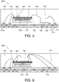
- FIG. 5 illustrates a diagram view of a semiconductor package 300 according to another embodiment of the invention.
- the semiconductor package 300 includes a carrier 210, the package module 120, the first adhesive layer 125, the second package body 130, at least one second conductive wire140, at least one second electronic element 150, the second adhesive layer 155 and at least one third electronic element 160.
- the semiconductor package 300 includes the features the same as or similar to that of the semiconductor package 200 expect that the carrier 210 has the structure different from that of the carrier 110.
- the carrier 210 is a second substrate including the structure the same as or similar to that of the first substrate 121 of the package module 120.
- the carrier 210 has, for example, single-layered structure or multi-layered structure.
- the carrier 210 has multi-layered structure including at least one dielectric layer 211, at least one conductive layer 212 and at least one conductive via 213.
- the dielectric layer 211 could be made of a material of non-conductive material, for example, epoxy or resin. Two of the conductive layers 212 are separated from each other by one of the dielectric layers 211, and electrically connected with each other by one of the conductive vias 213.
- first adhesive layer 125 is disposed between the carrier 210 and package surface 120b of the package module 120 for fixing the relative position between the carrier 210 and the second electronic element 150.
- the second adhesive layer 155 is disposed between the carrier 210 and the second electronic element 150 for fixing the relative position between the carrier 210 and the second electronic element 150.
- the carrier 210 has a third electrical surface 210u.
- the second package body 130 encapsulates the third electrical surface 210u of the carrier 210.
- the third electrical surface 210u is entirely covered by, for example, the package module 120 and the second electronic element 150 and the second package body 130.
- FIG. 6 illustrates a diagram view of a semiconductor package 400 according to another embodiment of the invention.
- the semiconductor package 400 includes the carrier 210, the package module 120, the first adhesive layer 125, the second package body 130, at least one second conductive wire140, at least one second electronic element 150, the second adhesive layer 155 and at least one third electronic element 160.
- the semiconductor package 400 includes the features the same as or similar to that of the semiconductor package 300 expect that the second electronic element 150 and the package module 120 are stacked to each other.
- FIGS. 7A to 7B illustrate diagram views of some package modules 120A to 120B according to some embodiments of the invention.
- the package module 120 of each of the semiconductor packages 100 to 400 could be replaced by one of the package modules 120A and 120B.
- the first substrate 121 of the package modules 120A has a through hole 120A1 and further includes a plug 120A2 filling up the through hole 120A1.
- the plug 120A2 protrudes respect to the second electrical surface 121u of the first substrate 121 and covers a portion of the second electrical surface 121u.
- the back surface 122b of the first electronic elements 122 is, for example, active surface. At least one of the first electronic elements 122 electrically connects with the second electrical surface 121u by one or some of the first conductive wires 123 encapsulated by the plug 120A2.
Landscapes
- Structures Or Materials For Encapsulating Or Coating Semiconductor Devices Or Solid State Devices (AREA)
- Wire Bonding (AREA)
- Control And Other Processes For Unpacking Of Materials (AREA)
- Structures For Mounting Electric Components On Printed Circuit Boards (AREA)
Abstract
Description
- The invention relates to a semiconductor package, and more particularly to a semiconductor package including a package module.
- Conventional semiconductor package includes a lead frame, a chip and a plurality of solder wires. The chip is disposed on the lead frame, and the solder wires electrically connect the chip with the lead frame. However, the conductive wires are boned to the lead frame which is thin, and thus it cause unreliability of bonding. Thus, how to bond the conductive wire in a way of reliability has become a prominent task for the industries.
- In an embodiment of the invention, a semiconductor package is provided. The semiconductor package includes a carrier, a package module and a second package body. The package module is disposed on the carrier and includes a first substrate, a first electronic element, a first conductive wire and a first package body. The first substrate has a first electrical surface facing the carrier and a second electrical surface opposite to the first electrical surface. The first electronic element is disposed on the first electrical surface. The first conductive wire connects the electronic element with the first electrical surface of the first substrate. The first package body encapsulates the first electrical surface, the first electronic element and the first solder wire. The second package body encapsulates the package module and a portion of the carrier.
- Numerous objects, features and advantages of the invention will be readily apparent upon a reading of the following detailed description of embodiments of the invention when taken in conjunction with the accompanying drawings. However, the drawings employed herein are for the purpose of descriptions and should not be regarded as limiting.
- The above objects and advantages of the invention will become more readily apparent to those ordinarily skilled in the art after reviewing the following detailed description and accompanying drawings, in which:
-
FIG. 1 illustrates a diagram view of a semiconductor package according to an embodiment of the invention; -
FIGS. 2 and 3 illustrate top views of configuration relationships between the package module and the second electronic element ofFIG. 1 ; -
FIG. 4 illustrates a diagram view of a semiconductor package according to another embodiment of the invention; -
FIG. 5 illustrates a diagram view of a semiconductor package according to another embodiment of the invention; -
FIG. 6 illustrates a diagram view of a semiconductor package according to another embodiment of the invention; and -
FIGS. 7A to 7B illustrate diagram views of some package modules according to some embodiments of the invention. - Referring to
FIGS. 1 to 3 ,FIG. 1 illustrates a diagram view of asemiconductor package 100 according to an embodiment of the invention, andFIGS. 2 and 3 illustrate top views of configuration relationships between thepackage module 120 and the secondelectronic element 150 ofFIG. 1 . - As illustrated in
FIG. 1 , thesemiconductor package 100 includes acarrier 110, apackage module 120, a firstadhesive layer 125, asecond package body 130, at least one second conductive wire140, at least one secondelectronic element 150, a secondadhesive layer 155 and at least one thirdelectronic element 160. In the present embodiment, the conductive wire could be made of a material including, for example, Au, Ag, Cu, Ni, etc. - The
package module 120 is disposed on thecarrier 110 and includes afirst substrate 121, at least one firstelectronic element 122, at least one firstconductive wire 123 and afirst package body 124. Thefirst substrate 121 has a firstelectrical surface 121b facing thecarrier 110 and a secondelectrical surface 121u opposite to the firstelectrical surface 121b. The firstelectronic elements 122 are disposed on the firstelectrical surface 121b. The firstconductive wires 123 connect the firstelectronic elements 122 with the firstelectrical surface 121b of thefirst substrate 121. Thefirst package body 124 encapsulates the firstelectrical surface 121b, the firstelectronic element 122 and the firstconductive wires 123. Thesecond package body 130 encapsulates thepackage module 120 and a portion of thecarrier 110. - Compared to the conductive wire being bonded to the
carrier 110, the conductive wire could more reliably (or steadily) be boned to thepackage module 120. In other words, due to thepackage module 120 provides a steady platform, it could increase the stability of the wire bonding and reduce the complexity of the wire bonding. In addition, due to theelectronic elements 122 being embedded in thefirst package body 124 in advance, the required number of the secondconductive wires 140 could be reduced and/or it could reduce the complexity of the wire bonding. - The
carrier 110 is, for example, lead frame. Thecarrier 110 includes a plurality ofinner leads 111, a plurality ofouter leads 112, agrounding ring 113 and adie pad 114, wherein each theouter lead 112 is connected to the correspondinginner lead 111, and thegrounding ring 113 could be connected to one or some of theinner leads 111. Theinner leads 111 and thegrounding ring 113 are encapsulated by thesecond package body 130, and theouter leads 112 protrude relative to thesecond package body 130 for electrically connected with an external electronic device. For example, Printed Circuit Board (PCB). The diepad 114 could carry thepackage module 120. - The
package module 120 further has apackage surface 120b away from the secondelectrical surface 121u. Thepackage surface 120b faces thecarrier 110, and the secondelectrical surface 121u faces away from thecarrier 110. - The
first substrate 121 has, for example, single-layered structure or multi-layered structure. In the present embodiment, thefirst substrate 121 has multi-layered structure including at least onedielectric layer 1211, at least oneconductive layer 1212 and at least one conductive via 1213. In addition, thedielectric layer 1211 could be made of a material of non-conductive material, for example, epoxy or resin. Two of theconductive layers 1212 are separated from each other by one of thedielectric layers 1211, and electrically connected with each other by one of theconductive vias 1213. Eachconductive layer 1212 includes at least one trace, and at least one conductive via 1213 connects with the traces of theconductive layers 1212. In addition, the bottommostconductive layer 1212 includes at least one trace and/or pad which form the firstelectrical surface 121b, and the bottommostconductive layer 1212 could be covered by solder mask (not illustrated) exposing the pad. The topmostdielectric layer 1212 includes at least one trace and/or pad which form the secondelectrical surface 121u, and the topmostconductive layer 1212 could be covered by solder mask (not illustrated) exposing the pad. - In another embodiment, the
first substrate 121 is, for example, a PCB, interposer, etc.; however, such exemplification is not meant to be for limiting. - Some of the first
electronic elements 122 could be stacked each other and/or a group of the stacked firstelectronic elements 122 and another group of the stacked firstelectronic elements 122 are disposed side by side. The number of a group of the stacked firstelectronic elements 122 is, for example, two, three or more. The number of the stacked group including the stacked firstelectronic elements 122 is, for example, one, two, three or more. In another embodiment, two firstelectronic elements 122 on which no firstelectronic element 122 is stacked are disposed with side by side, or one firstelectronic element 122 on which no firstelectronic element 122 is stacked and one stacked group of are disposed with side by side. - The first
electronic element 122 is, for example, memory chip, Sop (System on a Chip), etc.; however, such exemplification is not meant to be for limiting. In addition, the firstelectronic element 122 has anactive surface 122a facing thecarrier 110, that is, the firstelectronic element 122 is disposed in a reverse orientation and at least one of the first conductive wire123 electrically connects theactive surface 122a of at least one of the firstelectronic elements 122 with the firstelectrical surface 121b. The firstelectronic element 122 has aback surface 122b opposite to theactive surface 122a, and theback surface 122b faces thefirst substrate 121. In addition, thepackage module 120 further includes at least oneadhesive layer 126 disposed between theactive surface 122a of theelectronic element 122 with theback surface 122b of theelectronic element 122. - At least one of the first
conductive wires 123 electrically connect the firstelectronic elements 122 with the firstelectrical surface 121b of thefirst substrate 121. For example, at least one of the firstconductive wires 123 connects the firstelectronic elements 122 with the bottommostconductive layers 1212 forming the firstelectrical surface 121b. In another, at least one of the firstconductive wires 123 electrically connect two of the firstelectronic elements 122. - The
first package body 124 has thepackage surface 120b. Thepackage body 124 could be made of a material including, for example, a Novolac-based resin, an epoxy-based resin, a silicone-based resin, or another suitable encapsulant. Suitable fillers also can be included, such as powdered SiO2. Thepackage body 124 could be applied using any of a number of molding techniques, such as compression molding, injection molding, or transfer molding. - The first
adhesive layer 125 is disposed between thepackage module 120 and thecarrier 110. Furthermore, the firstadhesive layer 125 is disposed between thepackage surface 120b of thepackage module 120 and thedie pad 114 of thecarrier 110 for fixing the relative position between thecarrier 110 and thepackage module 120. - The
second package body 130 encapsulates thepackage module 120, a portion of thecarrier 110, the secondconductive wires 140, the secondelectronic element 150 and the thirdelectronic element 160. Thesecond package body 130 could be made of a material the same as or similar to thefirst package body 124. - At least one of the second
conductive wires 140 connect thepackage module 120 with the secondelectrical surface 121u of thefirst substrate 121 of thepackage module 120. For example, at least one of the secondconductive wires 140 connect thepackage module 120 with thetopmost dielectric layer 1212 forming the secondelectrical surface 121u. In addition, one of some of the secondconductive wires 140 electrically connect thegrounding ring 113 with the secondelectronic element 150. - The second
electronic element 150 is, for example, active chip, such as a SoC, etc. The secondelectronic element 150 is disposed on the secondelectrical surface 121u. - The second
adhesive layer 155 is disposed between thepackage module 120 and the secondelectronic element 150. Furthermore, the secondadhesive layer 155 is disposed between the secondelectrical surface 121u of thepackage module 120 and the secondelectronic element 150 for fixing the relative position between the secondelectronic element 150 and thepackage module 120. - The third
electronic element 160 is, for example, passive element, such as resistor, inductor and/or capacitor; however, such exemplification is not meant to be for limiting. The thirdelectronic element 160 is disposed on the secondelectrical surface 121u. - As illustrated in
FIGS. 2 and 3 , at least one portion of the secondelectronic element 150 could overlap thepackage module 120. For example, inFIG. 2 , a portion of the secondelectronic element 150 is disposed over thepackage module 120. InFIG. 3 , the entire of the secondelectronic element 150 is disposed over thepackage module 120. The position of the secondelectronic element 150 could be determined according to design of the wire bonding. - Referring to
FIG. 4, FIG. 4 illustrates a diagram view of asemiconductor package 200 according to another embodiment of the invention. - The
semiconductor package 200 includes thecarrier 110, thepackage module 120, the firstadhesive layer 125, thesecond package body 130, at least one second conductive wire140, at least one secondelectronic element 150, the secondadhesive layer 155 and at least one thirdelectronic element 160. - The
semiconductor package 200 includes the features the same as or similar to that of thesemiconductor package 100 expect that the secondelectronic element 150 and thepackage module 120 are disposed on thedie pad 114 of thecarrier 110 side by side. - Referring to
FIG. 5, FIG. 5 illustrates a diagram view of asemiconductor package 300 according to another embodiment of the invention. - The
semiconductor package 300 includes acarrier 210, thepackage module 120, the firstadhesive layer 125, thesecond package body 130, at least one second conductive wire140, at least one secondelectronic element 150, the secondadhesive layer 155 and at least one thirdelectronic element 160. - The
semiconductor package 300 includes the features the same as or similar to that of thesemiconductor package 200 expect that thecarrier 210 has the structure different from that of thecarrier 110. In the present embodiment, thecarrier 210 is a second substrate including the structure the same as or similar to that of thefirst substrate 121 of thepackage module 120. - The
carrier 210 has, for example, single-layered structure or multi-layered structure. In the present embodiment, thecarrier 210 has multi-layered structure including at least onedielectric layer 211, at least oneconductive layer 212 and at least one conductive via 213. In addition, thedielectric layer 211 could be made of a material of non-conductive material, for example, epoxy or resin. Two of theconductive layers 212 are separated from each other by one of thedielectric layers 211, and electrically connected with each other by one of theconductive vias 213. - In addition, the first
adhesive layer 125 is disposed between thecarrier 210 andpackage surface 120b of thepackage module 120 for fixing the relative position between thecarrier 210 and the secondelectronic element 150. The secondadhesive layer 155 is disposed between thecarrier 210 and the secondelectronic element 150 for fixing the relative position between thecarrier 210 and the secondelectronic element 150. - The
carrier 210 has a thirdelectrical surface 210u. Thesecond package body 130 encapsulates the thirdelectrical surface 210u of thecarrier 210. The thirdelectrical surface 210u is entirely covered by, for example, thepackage module 120 and the secondelectronic element 150 and thesecond package body 130. - Referring to
FIG. 6, FIG. 6 illustrates a diagram view of asemiconductor package 400 according to another embodiment of the invention. - The
semiconductor package 400 includes thecarrier 210, thepackage module 120, the firstadhesive layer 125, thesecond package body 130, at least one second conductive wire140, at least one secondelectronic element 150, the secondadhesive layer 155 and at least one thirdelectronic element 160. - The
semiconductor package 400 includes the features the same as or similar to that of thesemiconductor package 300 expect that the secondelectronic element 150 and thepackage module 120 are stacked to each other. - Referring to
FIGS. 7A to 7B, FIGS. 7A to 7B illustrate diagram views of somepackage modules 120A to 120B according to some embodiments of the invention. - The
package module 120 of each of the semiconductor packages 100 to 400 could be replaced by one of thepackage modules - As illustrated in
FIGS. 7A and 7B , thefirst substrate 121 of thepackage modules 120A has a through hole 120A1 and further includes a plug 120A2 filling up the through hole 120A1. The plug 120A2 protrudes respect to the secondelectrical surface 121u of thefirst substrate 121 and covers a portion of the secondelectrical surface 121u. In addition, in the present embodiment, theback surface 122b of the firstelectronic elements 122 is, for example, active surface. At least one of the firstelectronic elements 122 electrically connects with the secondelectrical surface 121u by one or some of the firstconductive wires 123 encapsulated by the plug 120A2. - While the invention has been described in terms of what is presently considered to be the most practical and preferred embodiments, it is to be understood that the invention needs not be limited to the disclosed embodiment. On the contrary, it is intended to cover various modifications and similar arrangements included within the scope of the appended claims which are to be accorded with the broadest interpretation so as to encompass all such modifications and similar structures.
Claims (13)
- A semiconductor package, comprising:a carrier;a package module disposed on the carrier, comprising:a first substrate having a first electrical surface facing the carrier and a second electrical surface opposite to the first electrical surface;a first electronic element disposed on the first electrical surface;a first conductive wire connecting the electronic element with the first electrical surface of the first substrate; anda first package body encapsulating the first electrical surface, the first electronic element and the first solder wire; anda second package body encapsulating the package module and a portion of the carrier.
- The semiconductor package as claimed in claim 1, wherein the carrier is lead frame.
- The semiconductor package as claimed in claim 1 or 2, wherein the carrier is a second substrate.
- The semiconductor package as claimed in any one of the preceding claims, further comprising:
a second conductive wire connecting the package module with the second electrical surface of the first substrate. - The semiconductor package as claimed in any one of the preceding claims, further comprising a plurality of the first electronic elements and a plurality of the first conductive wires, and one of the first conductive wires connects one of the first electronic elements with another of the first electronic elements.
- The semiconductor package as claimed in any one of the preceding claims, further comprising:a second electronic element disposed on the package module; anda second conductive wire connecting the second electronic element with the second electrical surface of the first substrate.
- The semiconductor package as claimed in any one of claims 1 to 3, further comprising:a second electronic element disposed on the carrier; anda second conductive wire connecting the second electronic element with the second electrical surface of the first substrate.
- The semiconductor package as claimed in claim 7, wherein the second electronic element and the package module are disposed side by side.
- The semiconductor package as claimed in any one of the preceding claims, wherein the first package body has a package surface; the semiconductor package further comprises:
an adhesive disposed between the package surface and the carrier. - The semiconductor package as claimed in any one of the preceding claims, wherein the first electronic element has an active surface facing the carrier, and the first conductive wire electrically connects the active surface with the first electrical surface.
- The semiconductor package as claimed in any one of claims 1 to 8, further comprising:
a first adhesive layer disposed between the carrier and the package module. - The semiconductor package as claimed in any one of claims 1 to 8 and claim 11, further comprising:
a second adhesive layer disposed between the package module and a second electronic element disposed on the package module. - The semiconductor package as claimed in any one of the preceding claims, wherein the carrier is a second substrate having a third electrical surface, and the second package body encapsulates the third electrical surface of the second substrate.
Priority Applications (1)
| Application Number | Priority Date | Filing Date | Title |
|---|---|---|---|
| EP25151616.7A EP4521457A3 (en) | 2021-02-22 | 2022-02-22 | Semiconductor package |
Applications Claiming Priority (3)
| Application Number | Priority Date | Filing Date | Title |
|---|---|---|---|
| US202163200210P | 2021-02-22 | 2021-02-22 | |
| US202163165307P | 2021-03-24 | 2021-03-24 | |
| US17/667,773 US12230598B2 (en) | 2021-02-22 | 2022-02-09 | Semiconductor package |
Related Child Applications (1)
| Application Number | Title | Priority Date | Filing Date |
|---|---|---|---|
| EP25151616.7A Division EP4521457A3 (en) | 2021-02-22 | 2022-02-22 | Semiconductor package |
Publications (1)
| Publication Number | Publication Date |
|---|---|
| EP4047650A1 true EP4047650A1 (en) | 2022-08-24 |
Family
ID=80447634
Family Applications (2)
| Application Number | Title | Priority Date | Filing Date |
|---|---|---|---|
| EP22158074.9A Withdrawn EP4047650A1 (en) | 2021-02-22 | 2022-02-22 | Semiconductor package |
| EP25151616.7A Pending EP4521457A3 (en) | 2021-02-22 | 2022-02-22 | Semiconductor package |
Family Applications After (1)
| Application Number | Title | Priority Date | Filing Date |
|---|---|---|---|
| EP25151616.7A Pending EP4521457A3 (en) | 2021-02-22 | 2022-02-22 | Semiconductor package |
Country Status (4)
| Country | Link |
|---|---|
| US (1) | US12230598B2 (en) |
| EP (2) | EP4047650A1 (en) |
| CN (1) | CN114975330A (en) |
| TW (1) | TWI796953B (en) |
Citations (5)
| Publication number | Priority date | Publication date | Assignee | Title |
|---|---|---|---|---|
| US20060138649A1 (en) * | 2002-10-08 | 2006-06-29 | Chippac, Inc. | Semiconductor multi-package module having inverted second package stacked over die-up flip-chip ball grid array (BGA) package |
| US20060175715A1 (en) * | 2005-02-07 | 2006-08-10 | Renesas Technology Corp. | Semiconductor device and capsule type semiconductor package |
| US20090001563A1 (en) * | 2007-06-27 | 2009-01-01 | Henry Descalzo Bathan | Integrated circuit package in package system with adhesiveless package attach |
| US20090236755A1 (en) * | 2008-03-19 | 2009-09-24 | Cheng-Ting Wu | Chip package structure |
| US20120326304A1 (en) * | 2011-06-24 | 2012-12-27 | Warren Robert W | Externally Wire Bondable Chip Scale Package in a System-in-Package Module |
Family Cites Families (5)
| Publication number | Priority date | Publication date | Assignee | Title |
|---|---|---|---|---|
| US6396130B1 (en) * | 2001-09-14 | 2002-05-28 | Amkor Technology, Inc. | Semiconductor package having multiple dies with independently biased back surfaces |
| TWI278947B (en) * | 2004-01-13 | 2007-04-11 | Samsung Electronics Co Ltd | A multi-chip package, a semiconductor device used therein and manufacturing method thereof |
| US8334171B2 (en) * | 2009-12-02 | 2012-12-18 | Stats Chippac Ltd. | Package system with a shielded inverted internal stacking module and method of manufacture thereof |
| JP2013021216A (en) * | 2011-07-13 | 2013-01-31 | Toshiba Corp | Laminate type semiconductor package |
| CN102403283B (en) * | 2011-11-25 | 2013-08-07 | 江苏长电科技股份有限公司 | Ball grid array packaging structure with basic islands and manufacturing method thereof |
-
2022
- 2022-02-09 US US17/667,773 patent/US12230598B2/en active Active
- 2022-02-14 TW TW111105284A patent/TWI796953B/en active
- 2022-02-18 CN CN202210150197.1A patent/CN114975330A/en active Pending
- 2022-02-22 EP EP22158074.9A patent/EP4047650A1/en not_active Withdrawn
- 2022-02-22 EP EP25151616.7A patent/EP4521457A3/en active Pending
Patent Citations (5)
| Publication number | Priority date | Publication date | Assignee | Title |
|---|---|---|---|---|
| US20060138649A1 (en) * | 2002-10-08 | 2006-06-29 | Chippac, Inc. | Semiconductor multi-package module having inverted second package stacked over die-up flip-chip ball grid array (BGA) package |
| US20060175715A1 (en) * | 2005-02-07 | 2006-08-10 | Renesas Technology Corp. | Semiconductor device and capsule type semiconductor package |
| US20090001563A1 (en) * | 2007-06-27 | 2009-01-01 | Henry Descalzo Bathan | Integrated circuit package in package system with adhesiveless package attach |
| US20090236755A1 (en) * | 2008-03-19 | 2009-09-24 | Cheng-Ting Wu | Chip package structure |
| US20120326304A1 (en) * | 2011-06-24 | 2012-12-27 | Warren Robert W | Externally Wire Bondable Chip Scale Package in a System-in-Package Module |
Also Published As
| Publication number | Publication date |
|---|---|
| EP4521457A3 (en) | 2025-06-18 |
| EP4521457A2 (en) | 2025-03-12 |
| CN114975330A (en) | 2022-08-30 |
| US20220270997A1 (en) | 2022-08-25 |
| US12230598B2 (en) | 2025-02-18 |
| TW202247389A (en) | 2022-12-01 |
| TWI796953B (en) | 2023-03-21 |
Similar Documents
| Publication | Publication Date | Title |
|---|---|---|
| US7298033B2 (en) | Stack type ball grid array package and method for manufacturing the same | |
| US6828665B2 (en) | Module device of stacked semiconductor packages and method for fabricating the same | |
| US6441483B1 (en) | Die stacking scheme | |
| US7166917B2 (en) | Semiconductor package having passive component disposed between semiconductor device and substrate | |
| US20060071315A1 (en) | Method of forming a stacked semiconductor package | |
| EP3147942B1 (en) | Semiconductor package, semiconductor device using the same and manufacturing method thereof | |
| JP2002016182A (en) | Wiring board, semiconductor device and package stack semiconductor device | |
| US11133284B2 (en) | Semiconductor package device | |
| US20090310322A1 (en) | Semiconductor Package | |
| KR20020061812A (en) | Ball grid array type multi chip package and stack package | |
| JP2009141169A (en) | Semiconductor device | |
| EP3128551A1 (en) | Semiconductor package and manufacturing method thereof | |
| JPH113969A (en) | Substrate components with stacked chip components | |
| US7652361B1 (en) | Land patterns for a semiconductor stacking structure and method therefor | |
| KR100673379B1 (en) | Laminated package and its manufacturing method | |
| EP4521457A2 (en) | Semiconductor package | |
| US7154171B1 (en) | Stacking structure for semiconductor devices using a folded over flexible substrate and method therefor | |
| JP2005057271A (en) | Semiconductor chip package having a functional part and a mounting part arranged horizontally on the same plane, and a stacked module thereof | |
| KR100650049B1 (en) | Stacked Packages Using Multi-Chip Packages | |
| KR101708870B1 (en) | Stacked semiconductor package and method for manufacturing the same | |
| US7781898B2 (en) | IC package reducing wiring layers on substrate and its chip carrier | |
| CN114975296B (en) | Semiconductor structure and manufacturing method | |
| KR200283421Y1 (en) | Stacked chip ceramic package device and stacked package device stacking the same | |
| KR20010018381A (en) | Circuit board using conductive ink and semiconductor package using the same | |
| KR940006578B1 (en) | Semicondoctor package and manufacturing method thereof |
Legal Events
| Date | Code | Title | Description |
|---|---|---|---|
| PUAI | Public reference made under article 153(3) epc to a published international application that has entered the european phase |
Free format text: ORIGINAL CODE: 0009012 |
|
| STAA | Information on the status of an ep patent application or granted ep patent |
Free format text: STATUS: REQUEST FOR EXAMINATION WAS MADE |
|
| 17P | Request for examination filed |
Effective date: 20220222 |
|
| AK | Designated contracting states |
Kind code of ref document: A1 Designated state(s): AL AT BE BG CH CY CZ DE DK EE ES FI FR GB GR HR HU IE IS IT LI LT LU LV MC MK MT NL NO PL PT RO RS SE SI SK SM TR |
|
| P01 | Opt-out of the competence of the unified patent court (upc) registered |
Effective date: 20230607 |
|
| STAA | Information on the status of an ep patent application or granted ep patent |
Free format text: STATUS: EXAMINATION IS IN PROGRESS |
|
| 17Q | First examination report despatched |
Effective date: 20240801 |
|
| STAA | Information on the status of an ep patent application or granted ep patent |
Free format text: STATUS: THE APPLICATION HAS BEEN WITHDRAWN |
|
| 18W | Application withdrawn |
Effective date: 20250130 |