EP4047413A1 - Liquid crystal display device - Google Patents
Liquid crystal display device Download PDFInfo
- Publication number
- EP4047413A1 EP4047413A1 EP20875719.5A EP20875719A EP4047413A1 EP 4047413 A1 EP4047413 A1 EP 4047413A1 EP 20875719 A EP20875719 A EP 20875719A EP 4047413 A1 EP4047413 A1 EP 4047413A1
- Authority
- EP
- European Patent Office
- Prior art keywords
- liquid crystal
- area
- pixel electrode
- crystal display
- pixel
- Prior art date
- Legal status (The legal status is an assumption and is not a legal conclusion. Google has not performed a legal analysis and makes no representation as to the accuracy of the status listed.)
- Granted
Links
Images




Classifications
-
- G—PHYSICS
- G02—OPTICS
- G02F—OPTICAL DEVICES OR ARRANGEMENTS FOR THE CONTROL OF LIGHT BY MODIFICATION OF THE OPTICAL PROPERTIES OF THE MEDIA OF THE ELEMENTS INVOLVED THEREIN; NON-LINEAR OPTICS; FREQUENCY-CHANGING OF LIGHT; OPTICAL LOGIC ELEMENTS; OPTICAL ANALOGUE/DIGITAL CONVERTERS
- G02F1/00—Devices or arrangements for the control of the intensity, colour, phase, polarisation or direction of light arriving from an independent light source, e.g. switching, gating or modulating; Non-linear optics
- G02F1/01—Devices or arrangements for the control of the intensity, colour, phase, polarisation or direction of light arriving from an independent light source, e.g. switching, gating or modulating; Non-linear optics for the control of the intensity, phase, polarisation or colour
- G02F1/13—Devices or arrangements for the control of the intensity, colour, phase, polarisation or direction of light arriving from an independent light source, e.g. switching, gating or modulating; Non-linear optics for the control of the intensity, phase, polarisation or colour based on liquid crystals, e.g. single liquid crystal display cells
- G02F1/133—Constructional arrangements; Operation of liquid crystal cells; Circuit arrangements
- G02F1/1333—Constructional arrangements; Manufacturing methods
- G02F1/1335—Structural association of cells with optical devices, e.g. polarisers or reflectors
- G02F1/133553—Reflecting elements
-
- G—PHYSICS
- G02—OPTICS
- G02F—OPTICAL DEVICES OR ARRANGEMENTS FOR THE CONTROL OF LIGHT BY MODIFICATION OF THE OPTICAL PROPERTIES OF THE MEDIA OF THE ELEMENTS INVOLVED THEREIN; NON-LINEAR OPTICS; FREQUENCY-CHANGING OF LIGHT; OPTICAL LOGIC ELEMENTS; OPTICAL ANALOGUE/DIGITAL CONVERTERS
- G02F1/00—Devices or arrangements for the control of the intensity, colour, phase, polarisation or direction of light arriving from an independent light source, e.g. switching, gating or modulating; Non-linear optics
- G02F1/01—Devices or arrangements for the control of the intensity, colour, phase, polarisation or direction of light arriving from an independent light source, e.g. switching, gating or modulating; Non-linear optics for the control of the intensity, phase, polarisation or colour
- G02F1/13—Devices or arrangements for the control of the intensity, colour, phase, polarisation or direction of light arriving from an independent light source, e.g. switching, gating or modulating; Non-linear optics for the control of the intensity, phase, polarisation or colour based on liquid crystals, e.g. single liquid crystal display cells
- G02F1/133—Constructional arrangements; Operation of liquid crystal cells; Circuit arrangements
- G02F1/1333—Constructional arrangements; Manufacturing methods
- G02F1/1343—Electrodes
- G02F1/134309—Electrodes characterised by their geometrical arrangement
-
- G—PHYSICS
- G02—OPTICS
- G02F—OPTICAL DEVICES OR ARRANGEMENTS FOR THE CONTROL OF LIGHT BY MODIFICATION OF THE OPTICAL PROPERTIES OF THE MEDIA OF THE ELEMENTS INVOLVED THEREIN; NON-LINEAR OPTICS; FREQUENCY-CHANGING OF LIGHT; OPTICAL LOGIC ELEMENTS; OPTICAL ANALOGUE/DIGITAL CONVERTERS
- G02F1/00—Devices or arrangements for the control of the intensity, colour, phase, polarisation or direction of light arriving from an independent light source, e.g. switching, gating or modulating; Non-linear optics
- G02F1/01—Devices or arrangements for the control of the intensity, colour, phase, polarisation or direction of light arriving from an independent light source, e.g. switching, gating or modulating; Non-linear optics for the control of the intensity, phase, polarisation or colour
- G02F1/13—Devices or arrangements for the control of the intensity, colour, phase, polarisation or direction of light arriving from an independent light source, e.g. switching, gating or modulating; Non-linear optics for the control of the intensity, phase, polarisation or colour based on liquid crystals, e.g. single liquid crystal display cells
- G02F1/133—Constructional arrangements; Operation of liquid crystal cells; Circuit arrangements
- G02F1/1333—Constructional arrangements; Manufacturing methods
- G02F1/1335—Structural association of cells with optical devices, e.g. polarisers or reflectors
- G02F1/133553—Reflecting elements
- G02F1/133555—Transflectors
-
- G—PHYSICS
- G02—OPTICS
- G02F—OPTICAL DEVICES OR ARRANGEMENTS FOR THE CONTROL OF LIGHT BY MODIFICATION OF THE OPTICAL PROPERTIES OF THE MEDIA OF THE ELEMENTS INVOLVED THEREIN; NON-LINEAR OPTICS; FREQUENCY-CHANGING OF LIGHT; OPTICAL LOGIC ELEMENTS; OPTICAL ANALOGUE/DIGITAL CONVERTERS
- G02F1/00—Devices or arrangements for the control of the intensity, colour, phase, polarisation or direction of light arriving from an independent light source, e.g. switching, gating or modulating; Non-linear optics
- G02F1/01—Devices or arrangements for the control of the intensity, colour, phase, polarisation or direction of light arriving from an independent light source, e.g. switching, gating or modulating; Non-linear optics for the control of the intensity, phase, polarisation or colour
- G02F1/13—Devices or arrangements for the control of the intensity, colour, phase, polarisation or direction of light arriving from an independent light source, e.g. switching, gating or modulating; Non-linear optics for the control of the intensity, phase, polarisation or colour based on liquid crystals, e.g. single liquid crystal display cells
- G02F1/133—Constructional arrangements; Operation of liquid crystal cells; Circuit arrangements
- G02F1/1333—Constructional arrangements; Manufacturing methods
-
- G—PHYSICS
- G02—OPTICS
- G02F—OPTICAL DEVICES OR ARRANGEMENTS FOR THE CONTROL OF LIGHT BY MODIFICATION OF THE OPTICAL PROPERTIES OF THE MEDIA OF THE ELEMENTS INVOLVED THEREIN; NON-LINEAR OPTICS; FREQUENCY-CHANGING OF LIGHT; OPTICAL LOGIC ELEMENTS; OPTICAL ANALOGUE/DIGITAL CONVERTERS
- G02F1/00—Devices or arrangements for the control of the intensity, colour, phase, polarisation or direction of light arriving from an independent light source, e.g. switching, gating or modulating; Non-linear optics
- G02F1/01—Devices or arrangements for the control of the intensity, colour, phase, polarisation or direction of light arriving from an independent light source, e.g. switching, gating or modulating; Non-linear optics for the control of the intensity, phase, polarisation or colour
- G02F1/13—Devices or arrangements for the control of the intensity, colour, phase, polarisation or direction of light arriving from an independent light source, e.g. switching, gating or modulating; Non-linear optics for the control of the intensity, phase, polarisation or colour based on liquid crystals, e.g. single liquid crystal display cells
- G02F1/133—Constructional arrangements; Operation of liquid crystal cells; Circuit arrangements
- G02F1/1333—Constructional arrangements; Manufacturing methods
- G02F1/133371—Cells with varying thickness of the liquid crystal layer
-
- G—PHYSICS
- G02—OPTICS
- G02F—OPTICAL DEVICES OR ARRANGEMENTS FOR THE CONTROL OF LIGHT BY MODIFICATION OF THE OPTICAL PROPERTIES OF THE MEDIA OF THE ELEMENTS INVOLVED THEREIN; NON-LINEAR OPTICS; FREQUENCY-CHANGING OF LIGHT; OPTICAL LOGIC ELEMENTS; OPTICAL ANALOGUE/DIGITAL CONVERTERS
- G02F1/00—Devices or arrangements for the control of the intensity, colour, phase, polarisation or direction of light arriving from an independent light source, e.g. switching, gating or modulating; Non-linear optics
- G02F1/01—Devices or arrangements for the control of the intensity, colour, phase, polarisation or direction of light arriving from an independent light source, e.g. switching, gating or modulating; Non-linear optics for the control of the intensity, phase, polarisation or colour
- G02F1/13—Devices or arrangements for the control of the intensity, colour, phase, polarisation or direction of light arriving from an independent light source, e.g. switching, gating or modulating; Non-linear optics for the control of the intensity, phase, polarisation or colour based on liquid crystals, e.g. single liquid crystal display cells
- G02F1/133—Constructional arrangements; Operation of liquid crystal cells; Circuit arrangements
- G02F1/1333—Constructional arrangements; Manufacturing methods
- G02F1/1337—Surface-induced orientation of the liquid crystal molecules, e.g. by alignment layers
- G02F1/133707—Structures for producing distorted electric fields, e.g. bumps, protrusions, recesses, slits in pixel electrodes
-
- G—PHYSICS
- G02—OPTICS
- G02F—OPTICAL DEVICES OR ARRANGEMENTS FOR THE CONTROL OF LIGHT BY MODIFICATION OF THE OPTICAL PROPERTIES OF THE MEDIA OF THE ELEMENTS INVOLVED THEREIN; NON-LINEAR OPTICS; FREQUENCY-CHANGING OF LIGHT; OPTICAL LOGIC ELEMENTS; OPTICAL ANALOGUE/DIGITAL CONVERTERS
- G02F1/00—Devices or arrangements for the control of the intensity, colour, phase, polarisation or direction of light arriving from an independent light source, e.g. switching, gating or modulating; Non-linear optics
- G02F1/01—Devices or arrangements for the control of the intensity, colour, phase, polarisation or direction of light arriving from an independent light source, e.g. switching, gating or modulating; Non-linear optics for the control of the intensity, phase, polarisation or colour
- G02F1/13—Devices or arrangements for the control of the intensity, colour, phase, polarisation or direction of light arriving from an independent light source, e.g. switching, gating or modulating; Non-linear optics for the control of the intensity, phase, polarisation or colour based on liquid crystals, e.g. single liquid crystal display cells
- G02F1/133—Constructional arrangements; Operation of liquid crystal cells; Circuit arrangements
- G02F1/1333—Constructional arrangements; Manufacturing methods
- G02F1/1337—Surface-induced orientation of the liquid crystal molecules, e.g. by alignment layers
- G02F1/133742—Surface-induced orientation of the liquid crystal molecules, e.g. by alignment layers for homeotropic alignment
-
- G—PHYSICS
- G02—OPTICS
- G02F—OPTICAL DEVICES OR ARRANGEMENTS FOR THE CONTROL OF LIGHT BY MODIFICATION OF THE OPTICAL PROPERTIES OF THE MEDIA OF THE ELEMENTS INVOLVED THEREIN; NON-LINEAR OPTICS; FREQUENCY-CHANGING OF LIGHT; OPTICAL LOGIC ELEMENTS; OPTICAL ANALOGUE/DIGITAL CONVERTERS
- G02F1/00—Devices or arrangements for the control of the intensity, colour, phase, polarisation or direction of light arriving from an independent light source, e.g. switching, gating or modulating; Non-linear optics
- G02F1/01—Devices or arrangements for the control of the intensity, colour, phase, polarisation or direction of light arriving from an independent light source, e.g. switching, gating or modulating; Non-linear optics for the control of the intensity, phase, polarisation or colour
- G02F1/13—Devices or arrangements for the control of the intensity, colour, phase, polarisation or direction of light arriving from an independent light source, e.g. switching, gating or modulating; Non-linear optics for the control of the intensity, phase, polarisation or colour based on liquid crystals, e.g. single liquid crystal display cells
- G02F1/133—Constructional arrangements; Operation of liquid crystal cells; Circuit arrangements
- G02F1/136—Liquid crystal cells structurally associated with a semi-conducting layer or substrate, e.g. cells forming part of an integrated circuit
- G02F1/1362—Active matrix addressed cells
- G02F1/136227—Through-hole connection of the pixel electrode to the active element through an insulation layer
-
- G—PHYSICS
- G02—OPTICS
- G02F—OPTICAL DEVICES OR ARRANGEMENTS FOR THE CONTROL OF LIGHT BY MODIFICATION OF THE OPTICAL PROPERTIES OF THE MEDIA OF THE ELEMENTS INVOLVED THEREIN; NON-LINEAR OPTICS; FREQUENCY-CHANGING OF LIGHT; OPTICAL LOGIC ELEMENTS; OPTICAL ANALOGUE/DIGITAL CONVERTERS
- G02F2203/00—Function characteristic
- G02F2203/09—Function characteristic transflective
Definitions
- the present invention relates to a liquid crystal display device capable of transmission display and reflection display.
- a transflective liquid crystal display device capable of displaying images in both transmission mode and reflection mode has been known as a liquid crystal display device that is improved in outdoor visibility.
- a reflective metal film provided inside a liquid crystal cell is patterned to form a reflection area and a transmission area and combine reflection display by the reflection area and transmission display by the transmission area.
- a transparent step film or the like is provided in the reflection area to vary a cell gap (multigap) between the reflection area and the transmission area and thus optimize the optical characteristics (refer to patent literatures 1 and 2, for example).
- steps are formed between the reflection area and the transmission area to easily cause an alignment failure at the boundary of the steps and a light leakage from the boundary.
- the alignment failure makes an image rough and the light leakage reduces the contrast of display.
- the alignment failure is continued and the traces of the pressure will be left (patent literature 3).
- various methods are proposed, such as separating a pixel electrode (forming a slit) in a step portion between a reflection area and a transmission area in one pixel to form the reflection area and the transmission area independently (patent literature 4), controlling the height (patent literature 5) and inclination (patent literature 6) of a protrusion formed in the transmission area to control alignment, controlling alignment by an opening (hole) of the electrode in the reflection area of the electrode and a protrusion in the transmission area (patent literature 7), forming a recess in the reflection area and placing the protrusion in the recess (patent literature 8), and the like.
- the reflection area needs to be sufficiently large (for example, the area of the reflection area is 30% or more larger than that of the pixel electrode) and the brightness of transmission display is lowered.
- the alignment is controlled by the height and shape of a protrusion in the transmission area without increasing the area of the reflection area, the height and area of the protrusion are increased to lower the brightness of transmission display.
- the present invention provides a liquid crystal display device capable of inhibiting display quality from lowering without lowering the brightness of transmission display.
- a liquid crystal display device comprising:
- a liquid crystal display device capable of inhibiting display quality from lowering without lowering the brightness of transmission display, can be provided.
- FIG. 1 is a block diagram of a liquid crystal display device 1 according to a first embodiment of the present invention.
- the liquid crystal display device 1 includes a liquid crystal display panel 2, a backlight (illumination device) 3, a scan line driving circuit 4, a signal line driving circuit 5, a common electrode driver 6, a voltage generation circuit 7 and a control circuit 8.
- the liquid crystal display panel 2 includes a pixel array in which a plurality of pixels PX are arranged in a matrix.
- the liquid crystal display panel 2 includes a plurality of scan lines GL1 to GLm each extending in the row direction and a plurality of signal lines SL1 to SLn each extending in the column direction.
- the letters "m” and "n” each indicate an integer of two or more.
- Pixels PX are placed in intersection areas between the scan and signal lines GL and SL.
- the backlight 3 is a surface light source that irradiates the back surface of the liquid crystal display panel 2 with light.
- the backlight 3 for example, a direct type or a side light (edge light) type LED backlight is used.
- the scan line driving circuit 4 is electrically connected to the scan lines GL. Upon receiving a control signal from the control circuit 8, the scan line driving circuit 4 sends scan signals to the liquid crystal display panel 2 to turn on/off the switching elements included in the pixels PX.
- the signal line driving circuit 5 is electrically connected to the signal lines SL.
- the signal line driving circuit 5 receives a control signal and display data from the control circuit 8.
- the signal line driving circuit 5 sends gradation signals (drive voltages) corresponding to the display data to the liquid crystal display panel 2.
- the common electrode driver 6 generates a common voltage Vcom and applies it to the common electrode in the liquid crystal display panel 2.
- the voltage generation circuit 7 generates various voltages necessary for the operation of the liquid crystal display device 1 and applies them to the respective circuits.
- the control circuit 8 collectively controls the operation of the liquid crystal display device 1.
- the control circuit 8 externally receives image data DT and control signal CNT. Based on the image data DT, the control circuit 8 generates various control signals and sends the control signals to each of the circuits.
- the liquid crystal display panel 2 is a transflective liquid crystal display panel capable of transmission display and reflection display.
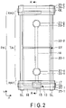
- FIG. 2 is a plan view of the liquid crystal display panel 2 according to the first embodiment.
- FIG. 3 is a sectional view of the liquid crystal display panel 2 taken along line A-A' in FIG. 2 .
- a portion corresponding to one pixel is extracted and actually, a plurality of pixels each corresponding to the pixel shown in FIG. 2 are arranged in a matrix.
- the liquid crystal display panel 2 includes a TFT substrate 10 on which a switching element (TFT), a pixel electrode and the like are formed, and a color filter substrate (CF substrate) 11 on which a color filter, a common electrode and the like are formed and which is opposed to the TFT substrate 10.
- TFT switching element
- CF substrate color filter substrate
- Each of the TFT and CF substrates 10 and 11 is configured by a transparent substrate (for example, a glass substrate or a plastic substrate).
- the liquid crystal layer 12 is filled between the TFT and CF substrates 10 and 11. Specifically, the liquid crystal layer 12 is sealed in a display area surrounded by the TFT and CF substrates 10 and 11 and a sealing member (not shown).
- the sealing member is made of an ultravioletcuring resin, a thermosetting resin, an ultraviolet-heat combination-type curing resin, or the like, and is applied to the TFT substrate 10 or the CF substrate 11 in the manufacturing process and then cured by ultraviolet irradiation, heating, or the like.
- the liquid crystal materials of the liquid crystal layer 12 vary in optical characteristics as the alignment of liquid crystal molecules is manipulated in accordance with an electric field applied between the TFT and CF substrates 10 and 11.
- the liquid crystal display panel 2 of the present embodiment is set in a vertical alignment (VA) mode using a VA type liquid crystal. That is, a negative (N-type) nematic liquid crystal having negative dielectric anisotropy is used as the liquid crystal layer 12.
- VA vertical alignment
- the liquid crystal layer 12 is vertically aligned in an initial state. When no voltage (no electric field) is applied to the liquid crystal layer 12, the major axes (directors) of liquid crystal molecules is aligned substantially vertically with respect to the main surface of the substrate. When a voltage is applied to the liquid crystal layer 12, the major axes of the liquid crystal molecules tilt toward the horizontal direction with respect to the main surface of the substrate.
- a switching element 13 is provided for each pixel on the liquid crystal layer 12 side of the TFT substrate 10.
- the switching element 13 for example, a thin film transistor (TFT) and an n-channel TFT are used.
- the TFT 13 includes a gate electrode functioning as a scan line, a gate insulating film provided on the gate electrode, a semiconductor layer provided on the gate insulating film, and a source electrode and a drain electrode which are provided on the semiconductor layer so as to be spaced from each other.
- a gate electrode GL is provided on the TFT substrate 10 to extend in the X direction.
- the gate electrode GL functions as a scan line GL.
- a plurality of pixels of one row arranged in the X direction are connected in common to one scan line GL.
- a gate insulating film 14 is provided on the TFT substrate 10 and the gate electrode GL.
- a semiconductor layer 15 is provided for each pixel.
- amorphous silicon is used as the semiconductor layer 15.
- a source electrode 16 and a drain electrode 17 are provided so as to be spaced from each other in a Y direction (which is orthogonal to the X direction).
- the source electrode 16 and drain electrode 17 each overlap the semiconductor layer 15.
- an n + -type semiconductor layer into which high-concentration n-type impurities are doped may be provided between them.
- an n + -type semiconductor layer may be provided between the drain electrode 17 and the semiconductor layer 15.
- connection electrode 18 is provided on the gate insulating film 14 to extend in the Y direction.
- the connection electrode 18 is electrically connected to the drain electrode 17.
- Signal lines SL are provided on the gate insulating film 14 to extend in the Y direction.
- the signal lines SL are each placed at a boundary between adjacent two pixels in the X direction.
- a plurality of pixels for one row arranged in the Y direction are connected in common to one signal line SL.
- the signal line SL is electrically connected to the source electrode 16.
- An insulating film 19 is provided on the source electrode 16, drain electrode 17, connection electrode 18, signal lines SL and gate insulating film 14.
- Reflecting films 20-1 and 20-2 are provided on the insulating film 19.
- the reflecting film 20-1 extends in the X direction to cover the TFT 13.
- the reflecting film 20-2 extends in the X direction to cover a TFT of a pixel adjacent to the pixel in the Y direction.
- the reflecting films 20-1 and 20-2 have a function of reflecting external light that is incident from the display surface side.
- An insulating film 21 is provided on the insulating film 19 and the reflecting films 20-1 and 20-2.
- Pixel electrodes 22-1 and 22-2 are provided on the insulating film 21.
- the pixel electrodes 22-1 and 22-2 are separated by a slit ST and arranged side by side in the Y direction.
- the pixel electrode 22-1 overlaps the reflecting film 20-1.
- the pixel electrode 22-2 overlaps the reflecting film 20-2.
- the planar view is viewing a pixel from above (from the substrate 11 side).
- the pixel electrode 22-1 is electrically connected to the connection electrode 18 by a contact 23-1.
- the pixel electrode 22-2 is electrically connected to the connection electrode 18 by a contact 23-2.
- a pixel area PA is defined by the pixel electrodes 22-1 and 22-2 and corresponds to an area of the combination of the pixel electrodes 22-1 and 22-2.
- an area of the combination of the reflection area RA1 and RA2 is a reflection area of the entire pixel.
- an area where neither of the reflecting films 20-1 and 20-2 is provided is a transmission area TA.
- the cell gap of the transmission area TA is defined as "d.”
- the cell gap is the thickness of the liquid crystal layer and is defined by the distance between the pixel electrode and the common electrode.
- an alignment film is provided on the pixel electrodes 22-1 and 22-2 and the insulating film 21 to control the alignment of the liquid crystal layer 12.
- the alignment film vertically aligns the liquid crystal molecules in the initial state of the liquid crystal layer 12.
- a color filter 24 is provided on the liquid crystal layer 12 side of the CF substrate 11.
- the color filter 24 is any one of a red filter, a green filter and a blue filter.
- Thickness adjusting layers 25-1 and 25-2 are provided on the color filter 24.
- the thickness adjusting layer 25-1 has approximately the same size (area) as the reflecting film 20-1, and is placed so as to overlap the reflecting film 20-1 in planar view.
- the thickness adjusting layer 25-2 has approximately the same size (area) as the reflecting film 20-2, and is placed so as to overlap the reflecting film 20-2 in planar view.
- the height (thickness) of each of the thickness adjusting layers 25-1 and 25-2 is defined as "t. "
- a common electrode 26 is provided on the color filter 24 and the thickness adjusting layers 25-1 and 25-2.
- the common electrode 26 is provided in common to a plurality of pixels.
- Protrusions 27-1 and 27-2 are provided on the common electrode 26.
- the protrusion 27-1 is disposed so as to overlap the contact 23-1 in planar view.
- the protrusion 27-2 is disposed so as to overlap the contact 23-2 in planar view.
- the projections 27-1 and 27-2 have a function of controlling the alignment of the liquid crystal layer 12.
- the protrusions 27-1 and 27-2 are provided to correspond to the pixel electrodes 22-1 and 22-2, respectively.
- the protrusion 27-1 is disposed closer to the center of the pixel than the thickness adjusting layer 25-1.
- the protrusion 27-2 is disposed closer to the center of the pixel than the thickness adjusting layer 25-2.
- the distance between the protrusion 27-1 and the thickness adjusting layer 25-1 and the distance between the protrusion 27-2 and the thickness adjusting layer 25-2 are defined as "L.”
- a multi-domain (alignment division) system namely, a multi-domain vertical alignment (MVA) mode is applied to the liquid crystal display panel 2.
- MVA multi-domain vertical alignment
- one pixel is divided into a plurality of areas (domains), and the direction in which liquid crystal molecules are inclined in each of the areas is changed.
- the protrusions 27-1 and 27-2 control the direction in which the liquid crystal molecules are inclined. That is, the liquid crystal molecules are inclined radially about each of the protrusions 27-1 and 27-2.
- the use of the MVA mode makes it possible to decrease the viewing angle dependence greatly and increase the viewing angle.
- openings formed in the common electrode 26 may be used.
- the openings have substantially the same size as the protrusions 27-1 and 27-2.
- an alignment film is provided on the common electrode 26 and the protrusions 27-1 and 27-2 to control the alignment of the liquid crystal layer 12.
- the alignment film vertically aligns the liquid crystal molecules in the initial state of the liquid crystal layer 12.
- a polarizing plate 28 is stacked on the TFT substrate 10 opposite to the liquid crystal layer 12, and a polarizing plate 29 is stacked on the CF substrate 11 opposite to the liquid crystal layer 12.
- the polarizing plates 28 and 29 are placed such that their transmission axes are orthogonal to each other, that is, in a crossed nicols state.
- a 1/4 wavelength plate may be provided between the TFT substrate 10 and the polarizing plate 28.
- a 1/4 wavelength plate may be provided between the CF substrate 11 and the polarizing plate 29.
- the gate electrode GL, source electrode 16, drain electrode 17 and signal lines SL for example, any one of aluminum (Al), molybdenum (Mo), chromium (Cr) and tungsten (W), or an alloy containing one or more of these is used.
- the connection electrode 18, pixel electrodes 22-1 and 22-2, contacts 23-1 and 23-2, and the common electrode 26 are formed of a transparent electrode, and, for example, indium tin oxide (ITO) is used.
- ITO indium tin oxide
- the reflecting films 20-1 and 20-2 for example, aluminum (Al) is used.
- the gate insulating film 14 and the insulating films 19 and 21 are formed of a transparent insulating material, such as silicon nitride (SiN).
- the thickness adjusting layers 25-1 and 25-2 are made of a transparent resin.
- the protrusions 27-1 and 27-2 are made of a transparent resin.
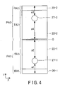
- FIG. 4 is a schematic diagram illustrating the conditions of the liquid crystal display panel 2.
- an area in which the pixel electrode 22-1 is provided is a partial pixel area PA1 and an area in which the pixel electrode 22-2 is provided is a partial pixel area PA2.
- the area corresponding to the combination of the partial pixel areas PA1 and PA2 is a pixel area PA.
- the boundary between the partial pixel areas PA1 and PA2 corresponds to the center line C of the pixel.
- an area in which the reflecting film 20-1 (and the thickness adjusting layer 25-1) is provided is a reflecting area RA1 and an area in which the reflecting film 20-1 is not provided is a transmitting area TA1.
- an area in which the reflecting film 20-2 (and the thickness adjusting layer 25-2) is provided is a reflecting area RA2 and an area in which the reflecting film 20-2 is not provided is a transmitting area TA2.
- An area corresponding to the combination of the reflecting areas RA1 and RA2 is a reflecting area RA of the entire pixel.
- An area corresponding to the combination of the transmitting areas TA1 and TA2 is a transmitting area TA of the entire pixel.
- the protrusion 27-1 is displaced from the center of the partial pixel area PA1 in the Y direction toward the reflecting area RA1.
- the protrusion 27-2 is displaced from the center of the partial pixel area PA2 in the Y direction toward the reflecting area RA2.
- the distance between the protrusion 27-1 and the end of the partial pixel area PA1 closer to the reflecting area RA1 is defined as a1.
- the distance between the protrusion 27-1 and the other end of the partial pixel area PA1 (the end closer to the center line of the pixel) is defined as a2.
- the distances al and a2 have the relation of "a1 ⁇ a2.”
- the distance between the protrusion 27-2 and the end of the partial pixel area PA2 closer to the reflecting area RA2 is defined as a3.
- the distance between the protrusion 27-2 and the other end of the partial pixel area PA2 (the end closer to the center line of the pixel) is defined as a4.
- the distances a3 and a4 have the relation of "a3 ⁇ a4.”
- the distances a3 and a4 have the relation of "a1 ⁇ a3" and "a2 ⁇ a4" in order to equalize the upper and lower viewing angle dependence in the Y direction.
- FIG. 5 is a graph showing the relationship between distance L between a thickness adjusting layer and a protrusion and surface pressure recovery time.
- the surface pressure means a case where a user applies pressure onto the display surface of the liquid crystal display panel 2 with his or her finger or a pen, and the surface pressure recovery time means time until a display failure, which is caused by the misalignment of a liquid crystal layer due to the surface pressure, is recovered.
- the horizontal axis represents the distance L ( ⁇ m) between the thickness adjusting layer and the protrusion and the vertical axis represents the surface pressure recovery time (sec).
- the cell gap d of the transmitting area is 3.8 ⁇ m
- the surface pressure is 0.5 MPa
- the surface pressure hold time is 5 sec.
- the flat gap means that there is no thickness adjusting layer and thus the gap of the liquid crystal layer is uniform.
- FIG. 6 is a modification to the graph of multigap shown in FIG. 5 .
- the horizontal axis represents parameter L ⁇ D ( ⁇ m) and the vertical axis represents surface pressure recovery time (sec).
- the parameter L ⁇ D is the product of the distance L between the thickness adjusting layer and the protrusion and the ratio D.
- the liquid crystal display panel 2 is capable of recovering a display failure due to surface pressure within 30 seconds.
- the distance L between the thickness adjusting layer and the protrusion, the cell gap d of the transmitting area, and the height t of the thickness adjusting layer are set so as to satisfy the condition of "L ⁇ D ⁇ 4.9 ⁇ m.
- the area of the transmitting area is set larger than that of the reflecting area.
- the area of the reflecting area is 30% or less of that of the partial pixel area.
- the area of the reflecting film 20-1 (or the thickness adjusting layer 25-1) is 30% or less of the area of the pixel electrode 22-1.
- the area of the reflecting film 20-1 is the area of the portion of the reflecting film 20-1 that overlaps the pixel electrode 22-1.
- the area of the reflecting film 20-2 (or the thickness adjusting layer 25-2) is 30% or less of the area of the pixel electrode 22-2.
- the area of the reflecting film 20-2 is the area of the portion of the reflecting film 20-2 that overlaps the pixel electrode 22-2.
- FIG. 7 is a schematic diagram of a liquid crystal display panel 2 according to the modification.
- the configuration of a partial pixel area PA1 is the same as that in the above-described embodiment. That is, the partial pixel area PA1 includes a reflecting area RA1 and a transmitting area TA1.
- the partial pixel area PA1 is provided with a pixel electrode 22-1, and the reflecting area RA1 is provided with a reflecting film 20-1.
- the partial pixel area PA2 is configured by the transmitting area TA1 in its entity.
- the partial pixel area PA2 is provided with a pixel electrode 22-2.
- the partial pixel area PA2 is provided with no reflecting area.
- a protrusion 27-2 is formed in the center of the partial pixel area PA2.
- the conditions of distances a1 and a2 in the partial pixel area PA1 are the same as those in the embodiment.
- the present embodiment can also be applied to the liquid crystal display panel 2 according to the modification in which a pixel includes one reflecting area.
- one pixel is divided into two partial pixel areas PA1 and PA2.
- the partial pixel area PA1 includes a reflecting area RA1 provided with a reflecting film 20-1 and a thickness adjusting layer 25-1, and a transmitting area TA1 other than the reflecting area RA1.
- the partial pixel area PA2 includes a reflecting area RA2 provided with a reflecting film 20-2 and a thickness adjusting layer 25-2, and a transmitting area TA2 other than the reflecting area RA2.
- the boundary between the reflecting area RA1 and the transmitting area TA1 is stepped by the thickness adjusting layer 25-1.
- the boundary between the reflecting area RA2 and the transmitting area TA2 is stepped by the thickness adjusting layer 25-2.
- the protrusion 27-1 for alignment control is located to shift from the center of the partial pixel area PA1 (pixel electrode 22-1) in the Y direction toward the thickness adjusting layer 25-1.
- the protrusion 27-2 is located to shift from the center of the partial pixel area PA2 (pixel electrode 22-2) in the Y direction toward the thickness adjusting layer 25-2.
- the first embodiment makes it possible to inhibit display quality from being lowered by alignment failure and to inhibit traces, which are caused by the alignment failure at the time of surface pressure, from being left, without decreasing brightness in transmission display.
- the above advantageous effects can be obtained more effectively if the area of the reflection area is, for example, 30% or less of the area of the partial pixel area.
- the second embodiment is directed to an example of a configuration example of a three-division pixel in which one pixel is divided into three partial pixels.
- FIG. 8 is a plan view of a liquid crystal display panel 2 according to the second embodiment.
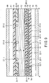
- FIG. 9 is a sectional view of the liquid crystal display panel 2 taken along line A-A' in FIG. 8 .
- Pixel electrodes 22-1, 22-2 and 22-3 are provided on an insulating film 21.
- the pixel electrodes 22-1, 22-2 and 22-3 are separated by slits ST.
- the pixel electrode 22-1, pixel electrode 22-3 and pixel electrode 22-2 are arranged in the Y direction in the order presented here.
- the pixel electrode 22-3 is electrically connected to a connection electrode 18 by a contact 23-3.
- a reflection film 20-1 overlaps the pixel electrode 22-1.
- a reflection film 20-2 overlaps the pixel electrode 22-2. No reflection film is provided below the pixel electrode 22-3.
- a protrusion 27-3 is provided on a common electrode 26. In planar view, the protrusion 27-3 is placed at the center of the pixel electrode 22-3 in the Y direction.
- a thickness adjusting layer 25-1 is provided on a color filter 24 and above the reflection film 20-1.
- a protrusion 27-1 is provided on the common electrode 26 and above the pixel electrode 22-1.
- a thickness adjusting layer 25-2 is provided on the color filter 24 and above the reflection film 20-2.
- a protrusion 27-2 is provided on the common electrode 26 and above the pixel electrode 22-2.
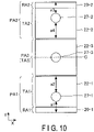
- FIG. 10 is a schematic diagram of the liquid crystal display panel 2 according to the second embodiment.
- an area where the pixel electrode 22-1 is provided is a partial pixel area PA1
- an area where the pixel electrode 22-2 is provided is a partial pixel area PA2
- an area where the pixel electrode 22-3 is provided is a partial pixel area PA3.
- the partial pixel area PA3 as a whole is configured by a transmission area TA3.
- the protrusion 27-3 is placed on the centerline C of the pixel.
- the conditions of distances al to a4 shown in FIG. 10 are the same as those in the first embodiment.
- the second embodiment also makes it possible to inhibit display quality from being lowered without decreasing brightness in transmission display.
- the present invention is not limited to the foregoing embodiments.
- the invention is reduced to practice, a variety of modifications can be made without departing from the spirit of the invention.
- the embodiments can be combined as appropriate, and advantageous effects can be obtained from the combination.
- the foregoing embodiments include a variety of inventions, and a variety of inventions can be extracted by selecting and combining a plurality of structural elements. For example, even though some of the structural elements are deleted from the embodiments, a configuration from which the structural elements are deleted can be extracted as an invention if the problem can be solved and an advantageous effect can be obtained.
Landscapes
- Physics & Mathematics (AREA)
- Nonlinear Science (AREA)
- Mathematical Physics (AREA)
- Chemical & Material Sciences (AREA)
- Crystallography & Structural Chemistry (AREA)
- General Physics & Mathematics (AREA)
- Optics & Photonics (AREA)
- Spectroscopy & Molecular Physics (AREA)
- Geometry (AREA)
- Liquid Crystal (AREA)
Abstract
Description
- The present invention relates to a liquid crystal display device capable of transmission display and reflection display.
- A transflective liquid crystal display device capable of displaying images in both transmission mode and reflection mode has been known as a liquid crystal display device that is improved in outdoor visibility. In the transflective liquid crystal display device, a reflective metal film provided inside a liquid crystal cell is patterned to form a reflection area and a transmission area and combine reflection display by the reflection area and transmission display by the transmission area. In addition, a transparent step film or the like is provided in the reflection area to vary a cell gap (multigap) between the reflection area and the transmission area and thus optimize the optical characteristics (refer to
patent literatures - In the liquid crystal display device having a multigap, steps are formed between the reflection area and the transmission area to easily cause an alignment failure at the boundary of the steps and a light leakage from the boundary. Thus, the following problems arise. The alignment failure makes an image rough and the light leakage reduces the contrast of display. In addition, when a user applies pressure to a display area with his or her finger or a pen (when the display area is pressed), the alignment failure is continued and the traces of the pressure will be left (patent literature 3).
- In order to solve the above problems, various methods are proposed, such as separating a pixel electrode (forming a slit) in a step portion between a reflection area and a transmission area in one pixel to form the reflection area and the transmission area independently (patent literature 4), controlling the height (patent literature 5) and inclination (patent literature 6) of a protrusion formed in the transmission area to control alignment, controlling alignment by an opening (hole) of the electrode in the reflection area of the electrode and a protrusion in the transmission area (patent literature 7), forming a recess in the reflection area and placing the protrusion in the recess (patent literature 8), and the like.
-
- Patent literature 1: Jpn. Pat. Appln. KOKAI Publication No.
2003-262852 - Patent literature 2: Jpn. Pat. Appln. KOKAI Publication No.
2003-270627 - Patent literature 3: International Publication No.
2005/111708 - Patent literature 4:
Japanese Patent No. 3900123 - Patent literature 5:
Japanese Patent No. 4432371 - Patent literature 6:
Japanese Patent No. 3903980 - Patent literature 7:
Japanese Patent No. 4182748 - Patent literature 8:
Japanese Patent No. 4123208 - However, the following problems arise. When a pixel electrode is separated by a slit between a reflection area and a transmission area in one pixel and when the alignment of the reflection area is controlled by a protrusion, an opening (hole) of the electrode and the like, the reflection area needs to be sufficiently large (for example, the area of the reflection area is 30% or more larger than that of the pixel electrode) and the brightness of transmission display is lowered. Similarly, even when the alignment is controlled by the height and shape of a protrusion in the transmission area without increasing the area of the reflection area, the height and area of the protrusion are increased to lower the brightness of transmission display.
- The present invention provides a liquid crystal display device capable of inhibiting display quality from lowering without lowering the brightness of transmission display.
- According to an aspect of the present invention, there is provided a liquid crystal display device comprising:
- first and second substrates;
- a liquid crystal layer interposed between the first and second substrates and set in vertical alignment (VA) when no electric field is applied;
- a switching element provided on the first substrate;
- a connection electrode provided on the first substrate, connected to the switching element, and extending in a first direction;
- a first reflection film provided above the switching element with an insulating film therebetween;
- a first pixel electrode provided above the first reflection film with an insulating film therebetween and overlapping the first reflection film in planar view;
- a second pixel electrode located adjacent to the first pixel electrode in the first direction;
- first and second contacts which connect the first and second pixel electrodes to the connection electrode;
- a first thickness adjusting layer provided on the second substrate and overlapping the first reflection film in planar view;
- a common electrode provided on the second substrate and the first thickness adjusting layer; and
- first and second protrusions provided on the common electrode and corresponding to the first and second pixel electrodes, respectively,
- wherein the first protrusion is located to shift toward the first thickness adjusting layer from a center of the first pixel electrode in the first direction.
- According to the present invention, a liquid crystal display device capable of inhibiting display quality from lowering without lowering the brightness of transmission display, can be provided.
-
-
FIG. 1 is a block diagram of a liquid crystal display device according to a first embodiment. -
FIG. 2 is a plan view of a liquid crystal display panel according to the first embodiment. -
FIG. 3 is a sectional view of the liquid crystal display panel taken along line A-A' ofFIG. 2 . -
FIG. 4 is a schematic diagram illustrating the conditions of the liquid crystal display panel. -
FIG. 5 is a graph showing the relationship between a distance between a thickness adjusting layer and a protrusion and surface pressure recovery time. -
FIG. 6 is a modification to the graph of multigap shown inFIG. 5 . -
FIG. 7 is a schematic diagram of a liquid crystal display panel according to a modification. -
FIG. 8 is a plan view of a liquid crystal display panel according to a second embodiment. -
FIG. 9 is a sectional view of the liquid crystal display panel taken along line A-A' ofFIG. 8 . -
FIG. 10 is a schematic diagram of the liquid crystal display panel according to the second embodiment. - Embodiments will be described below with reference to the drawings. The drawings are schematic or conceptual, and the dimension, ratio, or the like in each of the drawings is not necessarily the same as the actual one. The drawings may include portions that differ in the relationship in dimensions and in the ratio even though the portions are the same. Some of the embodiments exemplify a device and a method for embodying the technical concept of the present invention, and the technical concept is not specified by the shape, configuration, placement, etc. of the components. In the following descriptions, the elements having the same function and configuration are denoted by the same sign and their descriptions will be repeated only when necessary.
-
FIG. 1 is a block diagram of a liquidcrystal display device 1 according to a first embodiment of the present invention. The liquidcrystal display device 1 includes a liquidcrystal display panel 2, a backlight (illumination device) 3, a scanline driving circuit 4, a signalline driving circuit 5, acommon electrode driver 6, avoltage generation circuit 7 and acontrol circuit 8. - The liquid
crystal display panel 2 includes a pixel array in which a plurality of pixels PX are arranged in a matrix. The liquidcrystal display panel 2 includes a plurality of scan lines GL1 to GLm each extending in the row direction and a plurality of signal lines SL1 to SLn each extending in the column direction. The letters "m" and "n" each indicate an integer of two or more. Pixels PX are placed in intersection areas between the scan and signal lines GL and SL. - The
backlight 3 is a surface light source that irradiates the back surface of the liquidcrystal display panel 2 with light. As thebacklight 3, for example, a direct type or a side light (edge light) type LED backlight is used. - The scan
line driving circuit 4 is electrically connected to the scan lines GL. Upon receiving a control signal from thecontrol circuit 8, the scanline driving circuit 4 sends scan signals to the liquidcrystal display panel 2 to turn on/off the switching elements included in the pixels PX. - The signal
line driving circuit 5 is electrically connected to the signal lines SL. The signalline driving circuit 5 receives a control signal and display data from thecontrol circuit 8. In response to the control signal, the signalline driving circuit 5 sends gradation signals (drive voltages) corresponding to the display data to the liquidcrystal display panel 2. - The
common electrode driver 6 generates a common voltage Vcom and applies it to the common electrode in the liquidcrystal display panel 2. Thevoltage generation circuit 7 generates various voltages necessary for the operation of the liquidcrystal display device 1 and applies them to the respective circuits. - The
control circuit 8 collectively controls the operation of the liquidcrystal display device 1. Thecontrol circuit 8 externally receives image data DT and control signal CNT. Based on the image data DT, thecontrol circuit 8 generates various control signals and sends the control signals to each of the circuits. - [1-2] Configuration of Liquid
Crystal Display Panel 2 The liquidcrystal display panel 2 according to the present embodiment is a transflective liquid crystal display panel capable of transmission display and reflection display. -
FIG. 2 is a plan view of the liquidcrystal display panel 2 according to the first embodiment.FIG. 3 is a sectional view of the liquidcrystal display panel 2 taken along line A-A' inFIG. 2 . InFIG. 2 , a portion corresponding to one pixel is extracted and actually, a plurality of pixels each corresponding to the pixel shown inFIG. 2 are arranged in a matrix. - The liquid
crystal display panel 2 includes aTFT substrate 10 on which a switching element (TFT), a pixel electrode and the like are formed, and a color filter substrate (CF substrate) 11 on which a color filter, a common electrode and the like are formed and which is opposed to theTFT substrate 10. Each of the TFT andCF substrates - The
liquid crystal layer 12 is filled between the TFT andCF substrates liquid crystal layer 12 is sealed in a display area surrounded by the TFT andCF substrates TFT substrate 10 or theCF substrate 11 in the manufacturing process and then cured by ultraviolet irradiation, heating, or the like. - The liquid crystal materials of the
liquid crystal layer 12 vary in optical characteristics as the alignment of liquid crystal molecules is manipulated in accordance with an electric field applied between the TFT andCF substrates crystal display panel 2 of the present embodiment is set in a vertical alignment (VA) mode using a VA type liquid crystal. That is, a negative (N-type) nematic liquid crystal having negative dielectric anisotropy is used as theliquid crystal layer 12. Theliquid crystal layer 12 is vertically aligned in an initial state. When no voltage (no electric field) is applied to theliquid crystal layer 12, the major axes (directors) of liquid crystal molecules is aligned substantially vertically with respect to the main surface of the substrate. When a voltage is applied to theliquid crystal layer 12, the major axes of the liquid crystal molecules tilt toward the horizontal direction with respect to the main surface of the substrate. - First is a description of the configuration alongside the
TFT substrate 10. A switchingelement 13 is provided for each pixel on theliquid crystal layer 12 side of theTFT substrate 10. As the switchingelement 13, for example, a thin film transistor (TFT) and an n-channel TFT are used. As will be described later, theTFT 13 includes a gate electrode functioning as a scan line, a gate insulating film provided on the gate electrode, a semiconductor layer provided on the gate insulating film, and a source electrode and a drain electrode which are provided on the semiconductor layer so as to be spaced from each other. - A gate electrode GL is provided on the
TFT substrate 10 to extend in the X direction. The gate electrode GL functions as a scan line GL. A plurality of pixels of one row arranged in the X direction are connected in common to one scan line GL. Agate insulating film 14 is provided on theTFT substrate 10 and the gate electrode GL. - On the
gate insulating film 14, asemiconductor layer 15 is provided for each pixel. For example, amorphous silicon is used as thesemiconductor layer 15. - On the
semiconductor layer 15 and thegate insulating film 14, asource electrode 16 and adrain electrode 17 are provided so as to be spaced from each other in a Y direction (which is orthogonal to the X direction). Thesource electrode 16 anddrain electrode 17 each overlap thesemiconductor layer 15. In order to improve electrical connection between thesource electrode 16 and thesemiconductor layer 15, an n+-type semiconductor layer into which high-concentration n-type impurities are doped may be provided between them. Similarly, an n+-type semiconductor layer may be provided between thedrain electrode 17 and thesemiconductor layer 15. - A
connection electrode 18 is provided on thegate insulating film 14 to extend in the Y direction. Theconnection electrode 18 is electrically connected to thedrain electrode 17. - Signal lines SL are provided on the
gate insulating film 14 to extend in the Y direction. The signal lines SL are each placed at a boundary between adjacent two pixels in the X direction. A plurality of pixels for one row arranged in the Y direction are connected in common to one signal line SL. The signal line SL is electrically connected to thesource electrode 16. - An insulating
film 19 is provided on thesource electrode 16,drain electrode 17,connection electrode 18, signal lines SL andgate insulating film 14. - Reflecting films 20-1 and 20-2 are provided on the insulating
film 19. The reflecting film 20-1 extends in the X direction to cover theTFT 13. The reflecting film 20-2 extends in the X direction to cover a TFT of a pixel adjacent to the pixel in the Y direction. The reflecting films 20-1 and 20-2 have a function of reflecting external light that is incident from the display surface side. - An insulating
film 21 is provided on the insulatingfilm 19 and the reflecting films 20-1 and 20-2. - Pixel electrodes 22-1 and 22-2 are provided on the insulating
film 21. The pixel electrodes 22-1 and 22-2 are separated by a slit ST and arranged side by side in the Y direction. In planar view, the pixel electrode 22-1 overlaps the reflecting film 20-1. In planar view, the pixel electrode 22-2 overlaps the reflecting film 20-2. The planar view is viewing a pixel from above (from thesubstrate 11 side). - The pixel electrode 22-1 is electrically connected to the
connection electrode 18 by a contact 23-1. The pixel electrode 22-2 is electrically connected to theconnection electrode 18 by a contact 23-2. - A pixel area PA is defined by the pixel electrodes 22-1 and 22-2 and corresponds to an area of the combination of the pixel electrodes 22-1 and 22-2. An area where the pixel electrode 22-1 and the reflecting film 20-1 overlap, is a reflection area RA1. An area where the pixel electrode 22-2 and the reflecting film 20-2 overlap, is a reflection area RA2. In the pixel area PA, an area of the combination of the reflection area RA1 and RA2, is a reflection area of the entire pixel. In the pixel area PA, an area where neither of the reflecting films 20-1 and 20-2 is provided, is a transmission area TA. The cell gap of the transmission area TA is defined as "d." The cell gap is the thickness of the liquid crystal layer and is defined by the distance between the pixel electrode and the common electrode.
- Although not shown, an alignment film is provided on the pixel electrodes 22-1 and 22-2 and the insulating
film 21 to control the alignment of theliquid crystal layer 12. The alignment film vertically aligns the liquid crystal molecules in the initial state of theliquid crystal layer 12. - Next is a description of the configuration alongside the
CF substrate 11. Acolor filter 24 is provided on theliquid crystal layer 12 side of theCF substrate 11. Thecolor filter 24 is any one of a red filter, a green filter and a blue filter. - Thickness adjusting layers 25-1 and 25-2 are provided on the
color filter 24. The thickness adjusting layer 25-1 has approximately the same size (area) as the reflecting film 20-1, and is placed so as to overlap the reflecting film 20-1 in planar view. The thickness adjusting layer 25-2 has approximately the same size (area) as the reflecting film 20-2, and is placed so as to overlap the reflecting film 20-2 in planar view. The height (thickness) of each of the thickness adjusting layers 25-1 and 25-2 is defined as "t. " - A
common electrode 26 is provided on thecolor filter 24 and the thickness adjusting layers 25-1 and 25-2. Thecommon electrode 26 is provided in common to a plurality of pixels. - Protrusions 27-1 and 27-2 are provided on the
common electrode 26. The protrusion 27-1 is disposed so as to overlap the contact 23-1 in planar view. The protrusion 27-2 is disposed so as to overlap the contact 23-2 in planar view. The projections 27-1 and 27-2 have a function of controlling the alignment of theliquid crystal layer 12. The protrusions 27-1 and 27-2 are provided to correspond to the pixel electrodes 22-1 and 22-2, respectively. - The protrusion 27-1 is disposed closer to the center of the pixel than the thickness adjusting layer 25-1. The protrusion 27-2 is disposed closer to the center of the pixel than the thickness adjusting layer 25-2. The distance between the protrusion 27-1 and the thickness adjusting layer 25-1 and the distance between the protrusion 27-2 and the thickness adjusting layer 25-2 are defined as "L."
- In the present embodiment, a multi-domain (alignment division) system, namely, a multi-domain vertical alignment (MVA) mode is applied to the liquid
crystal display panel 2. In the MVA mode, one pixel is divided into a plurality of areas (domains), and the direction in which liquid crystal molecules are inclined in each of the areas is changed. The protrusions 27-1 and 27-2 control the direction in which the liquid crystal molecules are inclined. That is, the liquid crystal molecules are inclined radially about each of the protrusions 27-1 and 27-2. The use of the MVA mode makes it possible to decrease the viewing angle dependence greatly and increase the viewing angle. - Instead of the protrusions 27-1 and 27-2, openings formed in the
common electrode 26 may be used. In this case, the openings have substantially the same size as the protrusions 27-1 and 27-2. - Although not shown, an alignment film is provided on the
common electrode 26 and the protrusions 27-1 and 27-2 to control the alignment of theliquid crystal layer 12. The alignment film vertically aligns the liquid crystal molecules in the initial state of theliquid crystal layer 12. - A
polarizing plate 28 is stacked on theTFT substrate 10 opposite to theliquid crystal layer 12, and apolarizing plate 29 is stacked on theCF substrate 11 opposite to theliquid crystal layer 12. Thepolarizing plates TFT substrate 10 and thepolarizing plate 28. A 1/4 wavelength plate may be provided between theCF substrate 11 and thepolarizing plate 29. - As the gate electrode GL,
source electrode 16,drain electrode 17 and signal lines SL, for example, any one of aluminum (Al), molybdenum (Mo), chromium (Cr) and tungsten (W), or an alloy containing one or more of these is used. Theconnection electrode 18, pixel electrodes 22-1 and 22-2, contacts 23-1 and 23-2, and thecommon electrode 26 are formed of a transparent electrode, and, for example, indium tin oxide (ITO) is used. As the reflecting films 20-1 and 20-2, for example, aluminum (Al) is used. Thegate insulating film 14 and the insulatingfilms - [1-3] Conditions of Liquid
Crystal Display Panel 2 Next is a description of the conditions of the liquidcrystal display panel 2.FIG. 4 is a schematic diagram illustrating the conditions of the liquidcrystal display panel 2. - In
FIG. 4 , in the pixel, an area in which the pixel electrode 22-1 is provided is a partial pixel area PA1 and an area in which the pixel electrode 22-2 is provided is a partial pixel area PA2. The area corresponding to the combination of the partial pixel areas PA1 and PA2 is a pixel area PA. The boundary between the partial pixel areas PA1 and PA2 corresponds to the center line C of the pixel. - In the partial pixel area PA1, an area in which the reflecting film 20-1 (and the thickness adjusting layer 25-1) is provided is a reflecting area RA1 and an area in which the reflecting film 20-1 is not provided is a transmitting area TA1. In the partial pixel area PA2, an area in which the reflecting film 20-2 (and the thickness adjusting layer 25-2) is provided is a reflecting area RA2 and an area in which the reflecting film 20-2 is not provided is a transmitting area TA2. An area corresponding to the combination of the reflecting areas RA1 and RA2 is a reflecting area RA of the entire pixel. An area corresponding to the combination of the transmitting areas TA1 and TA2 is a transmitting area TA of the entire pixel.
- In planar view, the protrusion 27-1 is displaced from the center of the partial pixel area PA1 in the Y direction toward the reflecting area RA1. In planar view, the protrusion 27-2 is displaced from the center of the partial pixel area PA2 in the Y direction toward the reflecting area RA2.
- The following are specific definitions. The distance between the protrusion 27-1 and the end of the partial pixel area PA1 closer to the reflecting area RA1 is defined as a1. The distance between the protrusion 27-1 and the other end of the partial pixel area PA1 (the end closer to the center line of the pixel) is defined as a2. The distances al and a2 have the relation of "a1 < a2."
- The distance between the protrusion 27-2 and the end of the partial pixel area PA2 closer to the reflecting area RA2 is defined as a3. The distance between the protrusion 27-2 and the other end of the partial pixel area PA2 (the end closer to the center line of the pixel) is defined as a4. The distances a3 and a4 have the relation of "a3 < a4." Preferably, the distances a3 and a4 have the relation of "a1 ≈ a3" and "a2 ≒ a4" in order to equalize the upper and lower viewing angle dependence in the Y direction.
-
FIG. 5 is a graph showing the relationship between distance L between a thickness adjusting layer and a protrusion and surface pressure recovery time. The surface pressure means a case where a user applies pressure onto the display surface of the liquidcrystal display panel 2 with his or her finger or a pen, and the surface pressure recovery time means time until a display failure, which is caused by the misalignment of a liquid crystal layer due to the surface pressure, is recovered. InFIG. 5 , the horizontal axis represents the distance L (µm) between the thickness adjusting layer and the protrusion and the vertical axis represents the surface pressure recovery time (sec). The cell gap d of the transmitting area is 3.8 µm, the surface pressure is 0.5 MPa, and the surface pressure hold time is 5 sec. The graph ofFIG. 5 shows (1) a flat gap, (2) a multigap and a reflecting area cell gap of 2.5 µm, and (3) a multigap and a reflecting area cell gap of 2.2 µm. The flat gap means that there is no thickness adjusting layer and thus the gap of the liquid crystal layer is uniform. -
FIG. 6 is a modification to the graph of multigap shown inFIG. 5 . InFIG. 6 , the horizontal axis represents parameter L × D (µm) and the vertical axis represents surface pressure recovery time (sec). The ratio of height t of the thickness adjusting layer to cell gap d of the transmitting area is defined as D. That is, "D = t/d." The parameter L × D is the product of the distance L between the thickness adjusting layer and the protrusion and the ratio D. By modifying the graph ofFIG. 5 using the parameters L × D, the surface pressure recovery time can be defined uniquely in a plurality of multigaps. The curve inFIG. 6 is obtained by fitting using a function of "ax/(b-x)." - In the present embodiment, the liquid
crystal display panel 2 is capable of recovering a display failure due to surface pressure within 30 seconds. In this case, the distance L between the thickness adjusting layer and the protrusion, the cell gap d of the transmitting area, and the height t of the thickness adjusting layer are set so as to satisfy the condition of "L × D ≦ 4.9 µm. " - In the present embodiment, the area of the transmitting area is set larger than that of the reflecting area. For example, the area of the reflecting area is 30% or less of that of the partial pixel area. In other words, the area of the reflecting film 20-1 (or the thickness adjusting layer 25-1) is 30% or less of the area of the pixel electrode 22-1. Referring to
FIG. 2 , the area of the reflecting film 20-1 is the area of the portion of the reflecting film 20-1 that overlaps the pixel electrode 22-1. Similarly, the area of the reflecting film 20-2 (or the thickness adjusting layer 25-2) is 30% or less of the area of the pixel electrode 22-2. Referring toFIG. 2 , the area of the reflecting film 20-2 is the area of the portion of the reflecting film 20-2 that overlaps the pixel electrode 22-2. - Next is a description of a modification.
FIG. 7 is a schematic diagram of a liquidcrystal display panel 2 according to the modification. - The configuration of a partial pixel area PA1 is the same as that in the above-described embodiment. That is, the partial pixel area PA1 includes a reflecting area RA1 and a transmitting area TA1. The partial pixel area PA1 is provided with a pixel electrode 22-1, and the reflecting area RA1 is provided with a reflecting film 20-1.
- The partial pixel area PA2 is configured by the transmitting area TA1 in its entity. The partial pixel area PA2 is provided with a pixel electrode 22-2. The partial pixel area PA2 is provided with no reflecting area. A protrusion 27-2 is formed in the center of the partial pixel area PA2.
- The conditions of distances a1 and a2 in the partial pixel area PA1 are the same as those in the embodiment.
- The present embodiment can also be applied to the liquid
crystal display panel 2 according to the modification in which a pixel includes one reflecting area. - In the first embodiment, one pixel is divided into two partial pixel areas PA1 and PA2. The partial pixel area PA1 includes a reflecting area RA1 provided with a reflecting film 20-1 and a thickness adjusting layer 25-1, and a transmitting area TA1 other than the reflecting area RA1. The partial pixel area PA2 includes a reflecting area RA2 provided with a reflecting film 20-2 and a thickness adjusting layer 25-2, and a transmitting area TA2 other than the reflecting area RA2. The boundary between the reflecting area RA1 and the transmitting area TA1 is stepped by the thickness adjusting layer 25-1. The boundary between the reflecting area RA2 and the transmitting area TA2 is stepped by the thickness adjusting layer 25-2. The protrusion 27-1 for alignment control is located to shift from the center of the partial pixel area PA1 (pixel electrode 22-1) in the Y direction toward the thickness adjusting layer 25-1. Similarly, the protrusion 27-2 is located to shift from the center of the partial pixel area PA2 (pixel electrode 22-2) in the Y direction toward the thickness adjusting layer 25-2.
- Therefore, the first embodiment makes it possible to inhibit display quality from being lowered by alignment failure and to inhibit traces, which are caused by the alignment failure at the time of surface pressure, from being left, without decreasing brightness in transmission display.
- When the area of the reflection area is small, the above advantageous effects can be obtained more effectively if the area of the reflection area is, for example, 30% or less of the area of the partial pixel area.
- The second embodiment is directed to an example of a configuration example of a three-division pixel in which one pixel is divided into three partial pixels.
FIG. 8 is a plan view of a liquidcrystal display panel 2 according to the second embodiment.FIG. 9 is a sectional view of the liquidcrystal display panel 2 taken along line A-A' inFIG. 8 . - Pixel electrodes 22-1, 22-2 and 22-3 are provided on an insulating
film 21. The pixel electrodes 22-1, 22-2 and 22-3 are separated by slits ST. The pixel electrode 22-1, pixel electrode 22-3 and pixel electrode 22-2 are arranged in the Y direction in the order presented here. - The pixel electrode 22-3 is electrically connected to a
connection electrode 18 by a contact 23-3. - In planar view, a reflection film 20-1 overlaps the pixel electrode 22-1. In planar view, a reflection film 20-2 overlaps the pixel electrode 22-2. No reflection film is provided below the pixel electrode 22-3.
- A protrusion 27-3 is provided on a
common electrode 26. In planar view, the protrusion 27-3 is placed at the center of the pixel electrode 22-3 in the Y direction. - As in the first embodiment, a thickness adjusting layer 25-1 is provided on a
color filter 24 and above the reflection film 20-1. A protrusion 27-1 is provided on thecommon electrode 26 and above the pixel electrode 22-1. A thickness adjusting layer 25-2 is provided on thecolor filter 24 and above the reflection film 20-2. A protrusion 27-2 is provided on thecommon electrode 26 and above the pixel electrode 22-2. -
FIG. 10 is a schematic diagram of the liquidcrystal display panel 2 according to the second embodiment. - In each pixel, an area where the pixel electrode 22-1 is provided is a partial pixel area PA1, an area where the pixel electrode 22-2 is provided is a partial pixel area PA2, and an area where the pixel electrode 22-3 is provided is a partial pixel area PA3. The partial pixel area PA3 as a whole is configured by a transmission area TA3. The protrusion 27-3 is placed on the centerline C of the pixel.
- The conditions of distances al to a4 shown in
FIG. 10 are the same as those in the first embodiment. The second embodiment also makes it possible to inhibit display quality from being lowered without decreasing brightness in transmission display. - The present invention is not limited to the foregoing embodiments. When the invention is reduced to practice, a variety of modifications can be made without departing from the spirit of the invention. The embodiments can be combined as appropriate, and advantageous effects can be obtained from the combination. Furthermore, the foregoing embodiments include a variety of inventions, and a variety of inventions can be extracted by selecting and combining a plurality of structural elements. For example, even though some of the structural elements are deleted from the embodiments, a configuration from which the structural elements are deleted can be extracted as an invention if the problem can be solved and an advantageous effect can be obtained.
Claims (9)
- A liquid crystal display device comprising:first and second substrates;a liquid crystal layer interposed between the first and second substrates and set in vertical alignment (VA) when no electric field is applied;a switching element provided on the first substrate;a connection electrode provided on the first substrate, connected to the switching element, and extending in a first direction;a first reflection film provided above the switching element with an insulating film therebetween;a first pixel electrode provided above the first reflection film with an insulating film therebetween and overlapping the first reflection film in planar view;a second pixel electrode located adjacent to the first pixel electrode in the first direction;first and second contacts which connect the first and second pixel electrodes to the connection electrode;a first thickness adjusting layer provided on the second substrate and overlapping the first reflection film in planar view;a common electrode provided on the second substrate and the first thickness adjusting layer; andfirst and second protrusions provided on the common electrode and corresponding to the first and second pixel electrodes, respectively,wherein the first protrusion is located to shift toward the first thickness adjusting layer from a center of the first pixel electrode in the first direction.
- The liquid crystal display device according to claim 1, further comprising:a second reflection film located at a same level as the first reflection film to overlap the second pixel electrode in planar view; anda second thickness adjusting layer provided on the second substrate to overlap the second reflection film in planar view,wherein the second protrusion is located to shift toward the second thickness adjusting layer from a center of the second pixel electrode in the first direction.
- The liquid crystal display device according to one of claims 1 and 2, wherein the first and second protrusions overlap the first and second contacts, respectively in planar view.
- The liquid crystal display device according to claim 1, wherein when a distance between the first protrusion and the first thickness adjusting layer is L, a height of the first thickness, adjusting layer is t, a thickness of the liquid crystal layer in a transmission area where no reflection film is formed is d, and a ratio of the height t to the thickness d is D (= t/d), L × D is 4.9 µm or less.
- The liquid crystal display device according to claim 1, wherein the first reflection film has an area that is 30% or less of an area of the first pixel electrode.
- The liquid crystal display device according to claim 2, wherein when a distance between the second protrusion and the second thickness adjusting layer is L, a height of the second thickness adjusting layer is t, a thickness of the liquid crystal layer in a transmission area where no reflection film is formed is d, and a ratio of the height t to the thickness d is D (= t/d), L × D is 4.9 µm or less.
- The liquid crystal display device according to claim 2, wherein the second reflection film has an area that is 30% or less of an area of the second pixel electrode.
- The liquid crystal display device according to one of claims 1 and 2, further comprising:a third pixel electrode located at a same level as the first pixel electrode and between the first pixel electrode and the second pixel electrode;a third contact which connects the third pixel electrode and the connection electrode; anda third protrusion provided on the common electrode to correspond to the third pixel electrode.
- The liquid crystal display device according to claim 8, wherein the third protrusion is located at a center of the third pixel electrode in the first direction.
Applications Claiming Priority (2)
| Application Number | Priority Date | Filing Date | Title |
|---|---|---|---|
| JP2019189202A JP7331614B2 (en) | 2019-10-16 | 2019-10-16 | liquid crystal display |
| PCT/JP2020/038780 WO2021075462A1 (en) | 2019-10-16 | 2020-10-14 | Liquid crystal display device |
Publications (3)
| Publication Number | Publication Date |
|---|---|
| EP4047413A1 true EP4047413A1 (en) | 2022-08-24 |
| EP4047413A4 EP4047413A4 (en) | 2023-10-25 |
| EP4047413B1 EP4047413B1 (en) | 2024-10-23 |
Family
ID=75486221
Family Applications (1)
| Application Number | Title | Priority Date | Filing Date |
|---|---|---|---|
| EP20875719.5A Active EP4047413B1 (en) | 2019-10-16 | 2020-10-14 | Liquid crystal display device |
Country Status (6)
| Country | Link |
|---|---|
| US (1) | US11940691B2 (en) |
| EP (1) | EP4047413B1 (en) |
| JP (1) | JP7331614B2 (en) |
| CN (1) | CN114556204B (en) |
| TW (1) | TWI760891B (en) |
| WO (1) | WO2021075462A1 (en) |
Families Citing this family (1)
| Publication number | Priority date | Publication date | Assignee | Title |
|---|---|---|---|---|
| CN112419954B (en) * | 2019-08-21 | 2025-02-28 | 群创光电股份有限公司 | Electronic Devices |
Family Cites Families (25)
| Publication number | Priority date | Publication date | Assignee | Title |
|---|---|---|---|---|
| JP2003262852A (en) | 2001-09-25 | 2003-09-19 | Seiko Epson Corp | Transflective / reflective liquid crystal device and electronic equipment using the same |
| JP2003270627A (en) | 2001-09-25 | 2003-09-25 | Seiko Epson Corp | Transflective / reflective liquid crystal device and electronic equipment using the same |
| JP4182748B2 (en) | 2002-12-20 | 2008-11-19 | セイコーエプソン株式会社 | Liquid crystal display device and electronic device |
| JP3753141B2 (en) * | 2002-12-25 | 2006-03-08 | セイコーエプソン株式会社 | Liquid crystal display device and electronic device |
| JP4432371B2 (en) | 2003-06-06 | 2010-03-17 | セイコーエプソン株式会社 | Liquid crystal display device and electronic device |
| JP3900123B2 (en) | 2003-07-30 | 2007-04-04 | セイコーエプソン株式会社 | Liquid crystal display device and electronic device |
| JP3858882B2 (en) | 2003-10-21 | 2006-12-20 | セイコーエプソン株式会社 | Liquid crystal display device and electronic device |
| JP3903980B2 (en) | 2003-11-06 | 2007-04-11 | セイコーエプソン株式会社 | Liquid crystal display device and electronic device |
| CN100460964C (en) | 2004-05-18 | 2009-02-11 | 夏普株式会社 | Liquid crystal display device and electronic apparatus having the same |
| JP4361844B2 (en) * | 2004-07-28 | 2009-11-11 | 富士通株式会社 | Liquid crystal display |
| KR20060015209A (en) * | 2004-08-13 | 2006-02-16 | 삼성전자주식회사 | Array substrate, manufacturing method thereof and display device having same |
| JP4123208B2 (en) | 2004-09-03 | 2008-07-23 | セイコーエプソン株式会社 | Liquid crystal display device, electronic equipment |
| JP4082418B2 (en) * | 2005-03-04 | 2008-04-30 | エプソンイメージングデバイス株式会社 | Liquid crystal device and electronic device |
| JP2007101874A (en) | 2005-10-04 | 2007-04-19 | Toshiba Matsushita Display Technology Co Ltd | Liquid crystal display element |
| JP2007139948A (en) * | 2005-11-16 | 2007-06-07 | Epson Imaging Devices Corp | Electro-optical device and electronic apparatus |
| JP4923847B2 (en) * | 2006-08-21 | 2012-04-25 | ソニー株式会社 | LCD panel |
| JP4910642B2 (en) * | 2006-11-02 | 2012-04-04 | ソニー株式会社 | LCD panel |
| KR101332154B1 (en) | 2006-12-13 | 2014-01-08 | 엘지디스플레이 주식회사 | liquid crystal display device and method of fabricating the same |
| TWI395030B (en) * | 2007-03-27 | 2013-05-01 | Au Optronics Corp | A pixel structure and a display panel and optoelectronic device comprising the pixel structure and the manufacturing methods thereof |
| CN101122698A (en) * | 2007-09-18 | 2008-02-13 | 友达光电股份有限公司 | Multi-domain liquid crystal display |
| TWI374325B (en) | 2008-08-19 | 2012-10-11 | Au Optronics Corp | Liquid crystal display panel and pixel structure thereof |
| KR20130049194A (en) * | 2010-07-29 | 2013-05-13 | 도판 인사츠 가부시키가이샤 | Color filter substrate for liquid crystal display device, and liquid crystal display device |
| WO2016151429A1 (en) * | 2015-03-23 | 2016-09-29 | Semiconductor Energy Laboratory Co., Ltd. | Display panel and information processing device |
| JP6531313B2 (en) | 2015-05-01 | 2019-06-19 | 凸版印刷株式会社 | Liquid crystal display |
| JP6891514B2 (en) * | 2017-01-27 | 2021-06-18 | 凸版印刷株式会社 | Liquid crystal display device |
-
2019
- 2019-10-16 JP JP2019189202A patent/JP7331614B2/en active Active
-
2020
- 2020-10-14 EP EP20875719.5A patent/EP4047413B1/en active Active
- 2020-10-14 WO PCT/JP2020/038780 patent/WO2021075462A1/en not_active Ceased
- 2020-10-14 CN CN202080072566.9A patent/CN114556204B/en active Active
- 2020-10-15 TW TW109135644A patent/TWI760891B/en active
-
2022
- 2022-04-07 US US17/715,489 patent/US11940691B2/en active Active
Also Published As
| Publication number | Publication date |
|---|---|
| TW202125061A (en) | 2021-07-01 |
| EP4047413A4 (en) | 2023-10-25 |
| WO2021075462A1 (en) | 2021-04-22 |
| US20220229332A1 (en) | 2022-07-21 |
| CN114556204B (en) | 2024-03-22 |
| US11940691B2 (en) | 2024-03-26 |
| EP4047413B1 (en) | 2024-10-23 |
| JP7331614B2 (en) | 2023-08-23 |
| TWI760891B (en) | 2022-04-11 |
| CN114556204A (en) | 2022-05-27 |
| JP2021063936A (en) | 2021-04-22 |
Similar Documents
| Publication | Publication Date | Title |
|---|---|---|
| EP2916166B1 (en) | Liquid crystal display device | |
| US7206050B2 (en) | IPS type LCD and method for fabricating the same | |
| US7209198B2 (en) | Color filter array substrate and fabricating method thereof | |
| KR102334808B1 (en) | Display panel | |
| GB2557085A (en) | VA type COA liquid crystal display panel | |
| US11009758B2 (en) | Display panel and display device | |
| CN101627334A (en) | Display device, driving device for display device, and electronic apparatus | |
| US8310642B2 (en) | Liquid crystal display with texture control portion between pixel and common electrodes and method thereof | |
| CN101609219A (en) | Liquid crystal display device and manufacturing method thereof | |
| JP2007334345A (en) | Method of providing a gap in a liquid crystal display panel | |
| JP2002311448A (en) | Liquid crystal display device and manufacturing method thereof | |
| US20160363823A1 (en) | Liquid crystal display | |
| CN112327530A (en) | Display panel and display device | |
| US11940691B2 (en) | Liquid crystal display device | |
| US10416488B2 (en) | Liquid crystal display having a plurality of pixel electrodes in one pixel region | |
| US11789323B2 (en) | Liquid crystal display device | |
| US7623210B2 (en) | LCD apparatus having insulating layer with increased thickness over and in the same direction as data line with pixel electrodes overlapping top surface thereof to prevent light leakage | |
| US8018561B2 (en) | Liquid crystal display element | |
| JP4519691B2 (en) | Liquid crystal display panel and liquid crystal display device including the same | |
| JP2010139919A (en) | Liquid crystal display panel for ecb mode | |
| WO2016143621A1 (en) | Liquid crystal display device | |
| KR20040013787A (en) | Liquid Crystal Display Panel and Method of Fabricating the same | |
| KR101386576B1 (en) | Liquid crystal display panel | |
| JPWO2009066402A1 (en) | Liquid crystal display device and manufacturing method thereof | |
| JP2010060994A (en) | Liquid crystal display element |
Legal Events
| Date | Code | Title | Description |
|---|---|---|---|
| STAA | Information on the status of an ep patent application or granted ep patent |
Free format text: STATUS: THE INTERNATIONAL PUBLICATION HAS BEEN MADE |
|
| PUAI | Public reference made under article 153(3) epc to a published international application that has entered the european phase |
Free format text: ORIGINAL CODE: 0009012 |
|
| STAA | Information on the status of an ep patent application or granted ep patent |
Free format text: STATUS: REQUEST FOR EXAMINATION WAS MADE |
|
| 17P | Request for examination filed |
Effective date: 20220413 |
|
| AK | Designated contracting states |
Kind code of ref document: A1 Designated state(s): AL AT BE BG CH CY CZ DE DK EE ES FI FR GB GR HR HU IE IS IT LI LT LU LV MC MK MT NL NO PL PT RO RS SE SI SK SM TR |
|
| DAV | Request for validation of the european patent (deleted) | ||
| DAX | Request for extension of the european patent (deleted) | ||
| REG | Reference to a national code |
Ref country code: DE Ref legal event code: R079 Free format text: PREVIOUS MAIN CLASS: G02F0001136800 Ipc: G02F0001133500 Ref document number: 602020040078 Country of ref document: DE |
|
| A4 | Supplementary search report drawn up and despatched |
Effective date: 20230921 |
|
| RIC1 | Information provided on ipc code assigned before grant |
Ipc: G02F 1/1333 20060101ALI20230915BHEP Ipc: G02F 1/1337 20060101ALI20230915BHEP Ipc: G02F 1/1335 20060101AFI20230915BHEP |
|
| GRAP | Despatch of communication of intention to grant a patent |
Free format text: ORIGINAL CODE: EPIDOSNIGR1 |
|
| STAA | Information on the status of an ep patent application or granted ep patent |
Free format text: STATUS: GRANT OF PATENT IS INTENDED |
|
| INTG | Intention to grant announced |
Effective date: 20240529 |
|
| GRAS | Grant fee paid |
Free format text: ORIGINAL CODE: EPIDOSNIGR3 |
|
| GRAA | (expected) grant |
Free format text: ORIGINAL CODE: 0009210 |
|
| STAA | Information on the status of an ep patent application or granted ep patent |
Free format text: STATUS: THE PATENT HAS BEEN GRANTED |
|
| AK | Designated contracting states |
Kind code of ref document: B1 Designated state(s): AL AT BE BG CH CY CZ DE DK EE ES FI FR GB GR HR HU IE IS IT LI LT LU LV MC MK MT NL NO PL PT RO RS SE SI SK SM TR |
|
| REG | Reference to a national code |
Ref country code: GB Ref legal event code: FG4D |
|
| REG | Reference to a national code |
Ref country code: CH Ref legal event code: EP |
|
| REG | Reference to a national code |
Ref country code: DE Ref legal event code: R096 Ref document number: 602020040078 Country of ref document: DE |
|
| REG | Reference to a national code |
Ref country code: IE Ref legal event code: FG4D |
|
| REG | Reference to a national code |
Ref country code: LT Ref legal event code: MG9D |
|
| REG | Reference to a national code |
Ref country code: NL Ref legal event code: MP Effective date: 20241023 |
|
| REG | Reference to a national code |
Ref country code: AT Ref legal event code: MK05 Ref document number: 1735318 Country of ref document: AT Kind code of ref document: T Effective date: 20241023 |
|
| PG25 | Lapsed in a contracting state [announced via postgrant information from national office to epo] |
Ref country code: NL Free format text: LAPSE BECAUSE OF FAILURE TO SUBMIT A TRANSLATION OF THE DESCRIPTION OR TO PAY THE FEE WITHIN THE PRESCRIBED TIME-LIMIT Effective date: 20241023 |
|
| PG25 | Lapsed in a contracting state [announced via postgrant information from national office to epo] |
Ref country code: NL Free format text: LAPSE BECAUSE OF FAILURE TO SUBMIT A TRANSLATION OF THE DESCRIPTION OR TO PAY THE FEE WITHIN THE PRESCRIBED TIME-LIMIT Effective date: 20241023 |
|
| PG25 | Lapsed in a contracting state [announced via postgrant information from national office to epo] |
Ref country code: IS Free format text: LAPSE BECAUSE OF FAILURE TO SUBMIT A TRANSLATION OF THE DESCRIPTION OR TO PAY THE FEE WITHIN THE PRESCRIBED TIME-LIMIT Effective date: 20250223 Ref country code: PT Free format text: LAPSE BECAUSE OF FAILURE TO SUBMIT A TRANSLATION OF THE DESCRIPTION OR TO PAY THE FEE WITHIN THE PRESCRIBED TIME-LIMIT Effective date: 20250224 Ref country code: HR Free format text: LAPSE BECAUSE OF FAILURE TO SUBMIT A TRANSLATION OF THE DESCRIPTION OR TO PAY THE FEE WITHIN THE PRESCRIBED TIME-LIMIT Effective date: 20241023 |
|
| PG25 | Lapsed in a contracting state [announced via postgrant information from national office to epo] |
Ref country code: FI Free format text: LAPSE BECAUSE OF FAILURE TO SUBMIT A TRANSLATION OF THE DESCRIPTION OR TO PAY THE FEE WITHIN THE PRESCRIBED TIME-LIMIT Effective date: 20241023 |
|
| PG25 | Lapsed in a contracting state [announced via postgrant information from national office to epo] |
Ref country code: BG Free format text: LAPSE BECAUSE OF FAILURE TO SUBMIT A TRANSLATION OF THE DESCRIPTION OR TO PAY THE FEE WITHIN THE PRESCRIBED TIME-LIMIT Effective date: 20241023 |
|
| PG25 | Lapsed in a contracting state [announced via postgrant information from national office to epo] |
Ref country code: ES Free format text: LAPSE BECAUSE OF FAILURE TO SUBMIT A TRANSLATION OF THE DESCRIPTION OR TO PAY THE FEE WITHIN THE PRESCRIBED TIME-LIMIT Effective date: 20241023 |
|
| PG25 | Lapsed in a contracting state [announced via postgrant information from national office to epo] |
Ref country code: NO Free format text: LAPSE BECAUSE OF FAILURE TO SUBMIT A TRANSLATION OF THE DESCRIPTION OR TO PAY THE FEE WITHIN THE PRESCRIBED TIME-LIMIT Effective date: 20250123 |
|
| PG25 | Lapsed in a contracting state [announced via postgrant information from national office to epo] |
Ref country code: LV Free format text: LAPSE BECAUSE OF FAILURE TO SUBMIT A TRANSLATION OF THE DESCRIPTION OR TO PAY THE FEE WITHIN THE PRESCRIBED TIME-LIMIT Effective date: 20241023 Ref country code: AT Free format text: LAPSE BECAUSE OF FAILURE TO SUBMIT A TRANSLATION OF THE DESCRIPTION OR TO PAY THE FEE WITHIN THE PRESCRIBED TIME-LIMIT Effective date: 20241023 Ref country code: GR Free format text: LAPSE BECAUSE OF FAILURE TO SUBMIT A TRANSLATION OF THE DESCRIPTION OR TO PAY THE FEE WITHIN THE PRESCRIBED TIME-LIMIT Effective date: 20250124 |
|
| PG25 | Lapsed in a contracting state [announced via postgrant information from national office to epo] |
Ref country code: PL Free format text: LAPSE BECAUSE OF FAILURE TO SUBMIT A TRANSLATION OF THE DESCRIPTION OR TO PAY THE FEE WITHIN THE PRESCRIBED TIME-LIMIT Effective date: 20241023 |
|
| PG25 | Lapsed in a contracting state [announced via postgrant information from national office to epo] |
Ref country code: RS Free format text: LAPSE BECAUSE OF FAILURE TO SUBMIT A TRANSLATION OF THE DESCRIPTION OR TO PAY THE FEE WITHIN THE PRESCRIBED TIME-LIMIT Effective date: 20250123 |
|
| PG25 | Lapsed in a contracting state [announced via postgrant information from national office to epo] |
Ref country code: SM Free format text: LAPSE BECAUSE OF FAILURE TO SUBMIT A TRANSLATION OF THE DESCRIPTION OR TO PAY THE FEE WITHIN THE PRESCRIBED TIME-LIMIT Effective date: 20241023 |
|
| PG25 | Lapsed in a contracting state [announced via postgrant information from national office to epo] |
Ref country code: DK Free format text: LAPSE BECAUSE OF FAILURE TO SUBMIT A TRANSLATION OF THE DESCRIPTION OR TO PAY THE FEE WITHIN THE PRESCRIBED TIME-LIMIT Effective date: 20241023 |
|
| PG25 | Lapsed in a contracting state [announced via postgrant information from national office to epo] |
Ref country code: EE Free format text: LAPSE BECAUSE OF FAILURE TO SUBMIT A TRANSLATION OF THE DESCRIPTION OR TO PAY THE FEE WITHIN THE PRESCRIBED TIME-LIMIT Effective date: 20241023 |
|
| PG25 | Lapsed in a contracting state [announced via postgrant information from national office to epo] |
Ref country code: RO Free format text: LAPSE BECAUSE OF FAILURE TO SUBMIT A TRANSLATION OF THE DESCRIPTION OR TO PAY THE FEE WITHIN THE PRESCRIBED TIME-LIMIT Effective date: 20241023 |
|
| REG | Reference to a national code |
Ref country code: DE Ref legal event code: R097 Ref document number: 602020040078 Country of ref document: DE |
|
| PG25 | Lapsed in a contracting state [announced via postgrant information from national office to epo] |
Ref country code: SK Free format text: LAPSE BECAUSE OF FAILURE TO SUBMIT A TRANSLATION OF THE DESCRIPTION OR TO PAY THE FEE WITHIN THE PRESCRIBED TIME-LIMIT Effective date: 20241023 |
|
| PG25 | Lapsed in a contracting state [announced via postgrant information from national office to epo] |
Ref country code: CZ Free format text: LAPSE BECAUSE OF FAILURE TO SUBMIT A TRANSLATION OF THE DESCRIPTION OR TO PAY THE FEE WITHIN THE PRESCRIBED TIME-LIMIT Effective date: 20241023 |
|
| PG25 | Lapsed in a contracting state [announced via postgrant information from national office to epo] |
Ref country code: IT Free format text: LAPSE BECAUSE OF FAILURE TO SUBMIT A TRANSLATION OF THE DESCRIPTION OR TO PAY THE FEE WITHIN THE PRESCRIBED TIME-LIMIT Effective date: 20241023 |
|
| PLBE | No opposition filed within time limit |
Free format text: ORIGINAL CODE: 0009261 |
|
| STAA | Information on the status of an ep patent application or granted ep patent |
Free format text: STATUS: NO OPPOSITION FILED WITHIN TIME LIMIT |
|
| PG25 | Lapsed in a contracting state [announced via postgrant information from national office to epo] |
Ref country code: SE Free format text: LAPSE BECAUSE OF FAILURE TO SUBMIT A TRANSLATION OF THE DESCRIPTION OR TO PAY THE FEE WITHIN THE PRESCRIBED TIME-LIMIT Effective date: 20241023 |
|
| 26N | No opposition filed |
Effective date: 20250724 |
|
| PGFP | Annual fee paid to national office [announced via postgrant information from national office to epo] |
Ref country code: FR Payment date: 20250908 Year of fee payment: 6 |
|
| PGFP | Annual fee paid to national office [announced via postgrant information from national office to epo] |
Ref country code: DE Payment date: 20250902 Year of fee payment: 6 |
|
| REG | Reference to a national code |
Ref country code: CH Ref legal event code: H13 Free format text: ST27 STATUS EVENT CODE: U-0-0-H10-H13 (AS PROVIDED BY THE NATIONAL OFFICE) Effective date: 20260527 |
|
| PG25 | Lapsed in a contracting state [announced via postgrant information from national office to epo] |
Ref country code: LU Free format text: LAPSE BECAUSE OF NON-PAYMENT OF DUE FEES Effective date: 20251014 |
|
| REG | Reference to a national code |
Ref country code: BE Ref legal event code: MM Effective date: 20251031 |
|
| GBPC | Gb: european patent ceased through non-payment of renewal fee |
Effective date: 20251014 |
|
| PG25 | Lapsed in a contracting state [announced via postgrant information from national office to epo] |
Ref country code: LT Free format text: LAPSE BECAUSE OF FAILURE TO SUBMIT A TRANSLATION OF THE DESCRIPTION OR TO PAY THE FEE WITHIN THE PRESCRIBED TIME-LIMIT Effective date: 20241023 |
|
| PG25 | Lapsed in a contracting state [announced via postgrant information from national office to epo] |
Ref country code: MC Free format text: LAPSE BECAUSE OF FAILURE TO SUBMIT A TRANSLATION OF THE DESCRIPTION OR TO PAY THE FEE WITHIN THE PRESCRIBED TIME-LIMIT Effective date: 20241023 |
|
| PG25 | Lapsed in a contracting state [announced via postgrant information from national office to epo] |
Ref country code: GB Free format text: LAPSE BECAUSE OF NON-PAYMENT OF DUE FEES Effective date: 20251014 |
|
| PG25 | Lapsed in a contracting state [announced via postgrant information from national office to epo] |
Ref country code: CH Free format text: LAPSE BECAUSE OF NON-PAYMENT OF DUE FEES Effective date: 20251031 Ref country code: BE Free format text: LAPSE BECAUSE OF NON-PAYMENT OF DUE FEES Effective date: 20251031 |