EP4046801A1 - Element substrate, liquid discharge head, and liquid discharge apparatus - Google Patents
Element substrate, liquid discharge head, and liquid discharge apparatus Download PDFInfo
- Publication number
- EP4046801A1 EP4046801A1 EP22155129.4A EP22155129A EP4046801A1 EP 4046801 A1 EP4046801 A1 EP 4046801A1 EP 22155129 A EP22155129 A EP 22155129A EP 4046801 A1 EP4046801 A1 EP 4046801A1
- Authority
- EP
- European Patent Office
- Prior art keywords
- memory element
- liquid discharge
- current
- write
- elements
- Prior art date
- Legal status (The legal status is an assumption and is not a legal conclusion. Google has not performed a legal analysis and makes no representation as to the accuracy of the status listed.)
- Pending
Links
Images


Classifications
-
- B—PERFORMING OPERATIONS; TRANSPORTING
- B41—PRINTING; LINING MACHINES; TYPEWRITERS; STAMPS
- B41J—TYPEWRITERS; SELECTIVE PRINTING MECHANISMS, i.e. MECHANISMS PRINTING OTHERWISE THAN FROM A FORME; CORRECTION OF TYPOGRAPHICAL ERRORS
- B41J2/00—Typewriters or selective printing mechanisms characterised by the printing or marking process for which they are designed
- B41J2/005—Typewriters or selective printing mechanisms characterised by the printing or marking process for which they are designed characterised by bringing liquid or particles selectively into contact with a printing material
- B41J2/01—Ink jet
- B41J2/015—Ink jet characterised by the jet generation process
- B41J2/04—Ink jet characterised by the jet generation process generating single droplets or particles on demand
- B41J2/045—Ink jet characterised by the jet generation process generating single droplets or particles on demand by pressure, e.g. electromechanical transducers
- B41J2/04501—Control methods or devices therefor, e.g. driver circuits, control circuits
- B41J2/04541—Specific driving circuit
-
- B—PERFORMING OPERATIONS; TRANSPORTING
- B41—PRINTING; LINING MACHINES; TYPEWRITERS; STAMPS
- B41J—TYPEWRITERS; SELECTIVE PRINTING MECHANISMS, i.e. MECHANISMS PRINTING OTHERWISE THAN FROM A FORME; CORRECTION OF TYPOGRAPHICAL ERRORS
- B41J2/00—Typewriters or selective printing mechanisms characterised by the printing or marking process for which they are designed
- B41J2/005—Typewriters or selective printing mechanisms characterised by the printing or marking process for which they are designed characterised by bringing liquid or particles selectively into contact with a printing material
- B41J2/01—Ink jet
- B41J2/015—Ink jet characterised by the jet generation process
- B41J2/04—Ink jet characterised by the jet generation process generating single droplets or particles on demand
- B41J2/045—Ink jet characterised by the jet generation process generating single droplets or particles on demand by pressure, e.g. electromechanical transducers
- B41J2/04501—Control methods or devices therefor, e.g. driver circuits, control circuits
- B41J2/04581—Control methods or devices therefor, e.g. driver circuits, control circuits controlling heads based on piezoelectric elements
-
- B—PERFORMING OPERATIONS; TRANSPORTING
- B41—PRINTING; LINING MACHINES; TYPEWRITERS; STAMPS
- B41J—TYPEWRITERS; SELECTIVE PRINTING MECHANISMS, i.e. MECHANISMS PRINTING OTHERWISE THAN FROM A FORME; CORRECTION OF TYPOGRAPHICAL ERRORS
- B41J2/00—Typewriters or selective printing mechanisms characterised by the printing or marking process for which they are designed
- B41J2/005—Typewriters or selective printing mechanisms characterised by the printing or marking process for which they are designed characterised by bringing liquid or particles selectively into contact with a printing material
- B41J2/01—Ink jet
- B41J2/135—Nozzles
- B41J2/14—Structure thereof only for on-demand ink jet heads
- B41J2/14016—Structure of bubble jet print heads
-
- G—PHYSICS
- G11—INFORMATION STORAGE
- G11C—STATIC STORES
- G11C17/00—Read-only memories programmable only once; Semi-permanent stores, e.g. manually-replaceable information cards
- G11C17/14—Read-only memories programmable only once; Semi-permanent stores, e.g. manually-replaceable information cards in which contents are determined by selectively establishing, breaking or modifying connecting links by permanently altering the state of coupling elements, e.g. PROM
- G11C17/16—Read-only memories programmable only once; Semi-permanent stores, e.g. manually-replaceable information cards in which contents are determined by selectively establishing, breaking or modifying connecting links by permanently altering the state of coupling elements, e.g. PROM using electrically-fusible links
-
- G—PHYSICS
- G11—INFORMATION STORAGE
- G11C—STATIC STORES
- G11C17/00—Read-only memories programmable only once; Semi-permanent stores, e.g. manually-replaceable information cards
- G11C17/14—Read-only memories programmable only once; Semi-permanent stores, e.g. manually-replaceable information cards in which contents are determined by selectively establishing, breaking or modifying connecting links by permanently altering the state of coupling elements, e.g. PROM
- G11C17/18—Auxiliary circuits, e.g. for writing into memory
-
- B—PERFORMING OPERATIONS; TRANSPORTING
- B41—PRINTING; LINING MACHINES; TYPEWRITERS; STAMPS
- B41J—TYPEWRITERS; SELECTIVE PRINTING MECHANISMS, i.e. MECHANISMS PRINTING OTHERWISE THAN FROM A FORME; CORRECTION OF TYPOGRAPHICAL ERRORS
- B41J2/00—Typewriters or selective printing mechanisms characterised by the printing or marking process for which they are designed
- B41J2/005—Typewriters or selective printing mechanisms characterised by the printing or marking process for which they are designed characterised by bringing liquid or particles selectively into contact with a printing material
- B41J2/01—Ink jet
- B41J2/015—Ink jet characterised by the jet generation process
- B41J2/04—Ink jet characterised by the jet generation process generating single droplets or particles on demand
- B41J2/045—Ink jet characterised by the jet generation process generating single droplets or particles on demand by pressure, e.g. electromechanical transducers
- B41J2/04501—Control methods or devices therefor, e.g. driver circuits, control circuits
- B41J2/0458—Control methods or devices therefor, e.g. driver circuits, control circuits controlling heads based on heating elements forming bubbles
-
- B—PERFORMING OPERATIONS; TRANSPORTING
- B41—PRINTING; LINING MACHINES; TYPEWRITERS; STAMPS
- B41J—TYPEWRITERS; SELECTIVE PRINTING MECHANISMS, i.e. MECHANISMS PRINTING OTHERWISE THAN FROM A FORME; CORRECTION OF TYPOGRAPHICAL ERRORS
- B41J2202/00—Embodiments of or processes related to ink-jet or thermal heads
- B41J2202/01—Embodiments of or processes related to ink-jet heads
- B41J2202/13—Heads having an integrated circuit
Definitions
- the present invention mainly relates to an element substrate.
- a liquid discharge head used in, for example, a printer using an inkjet printing method includes an element substrate on which a plurality of liquid discharge elements are arrayed (see Japanese Patent Laid-Open No. 2014-58130 ).
- the element substrate is provided with memory elements that store whether to permit driving of the individual liquid discharge elements.
- whether to permit driving of each or the liquid discharge elements is decided based on the presence/absence of write to a corresponding memory element. For example, if a liquid discharge element cannot be driven, another liquid discharge element can be driven to complement that.
- the memory element a so-called one time programmable memory that is a memory element configured to permit write only once, for example, an anti-fuse element can be used.
- the impedance value mainly, the electric resistance value
- Japanese Patent Laid-Open No. 2008-299989 a configuration capable of determining the presence/absence of write to a memory element by detecting a voltage generated by supplying a current to the memory element is described.
- this configuration for example, if the amount of the current supplied to the memory element varies due to a peripheral environment such as a temperature, the impedance value of the memory element may vary. There is room for improvement from the viewpoint of increasing the accuracy of the determination.
- the first aspect of the present invention provides an element substrate as specified in claims 1 to 10.
- the second aspect of the present invention provides a liquid discharge head as specified in claim 11.
- the third aspect of the present invention provides a liquid discharge apparatus as specified in claim 12.
- the printing apparatus may be a single function printer having only a printing function or may be a multi-function printer having a plurality of functions such as a printing function, a FAX function, and a scanner function.
- the printing apparatus may be a manufacturing device configured to manufacture, for example, a color filter, an electronic device, an optical device, a microstructure, or the like using a predetermined printing method.
- print in this specification should be interpreted in a broader sense.
- the mode of "print” is irrespective of whether or not the target to be formed on a print medium is significant information such as a character or graphic pattern, and is also irrespective of whether the target is manifested in a way that can be perceived visually by humans.
- Print media should also be interpreted in a broader sense, like “print”.
- the concept of "print media” includes sheet-shaped members used in general, and any material capable of receiving ink, including paper, fabrics, plastic films, metals, glass, ceramics, resins, wood, and leathers can be used.
- Ink should also be interpreted in a broader sense, like "print”.
- the concept of "ink” can include not only a liquid that is applied to a print medium to form an image, a design, a pattern, or the like but also an incidental liquid that can be provided to process a print medium or process ink (for example, coagulate or insolubilize color materials in ink applied to a print medium).
- this can be expressed "liquid” in place of "ink”.
- a printing apparatus may be referred to as a liquid discharge apparatus, a discharge apparatus, or the like.
- a printhead provided in the printing apparatus may be referred to as a liquid discharge head, a discharge head, or the like.
- a print element substrate provided in the printhead may be referred to as a liquid discharge element substrate or a discharge element substrate, or simply as an element substrate.
- each of a plurality of print elements arrayed on the print element substrate may be referred to as a liquid discharge element, a discharge element, or the like.
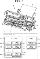
- Fig. 1 shows an example of the configuration of a printing apparatus 1 according to the first embodiment.
- the printing apparatus 1 includes a printhead 11 and a driver 12 and, in this embodiment, performs printing by an inkjet printing method.
- the printhead 11 is configured to execute printing on a predetermined print medium P, and includes a plurality of nozzles NZ and a print element substrate SB.
- Each nozzle NZ is a liquid discharge port that discharges a liquid received from a liquid tank TK that stores the liquid.
- the plurality of nozzles NZ are arrayed on a surface on a side to execute printing.
- the print element substrate SB includes a plurality of print elements PE corresponding to the plurality of nozzles NZ. When each print element PE is driven, a liquid is discharged from the corresponding nozzle NZ, thereby executing printing.
- a resistive element or simply called a heater
- a piezoelectric element may be used as the print element PE.
- the driver 12 includes a conveyance driver 121 and a head driver 122.
- the conveyance driver 121 conveys the print medium P set in the main body of the printing apparatus 1 to the printhead 11.
- the head driver 122 drives the printhead 11 with respect to the conveyed print medium P to cause the individual nozzles NZ to discharge the liquid, thereby performing printing.
- the printhead 11 is a serial head that performs printing on the print medium P while scanning in a direction crossing the conveyance direction of the print medium P.
- the printhead 11 may be a line head capable of printing at once on the whole region of the print medium P in the widthwise direction.
- Fig. 2 shows an example of the configuration of the print element substrate SB.
- the print element substrate SB In a planar view (a viewpoint in a direction vertical to the principal plane, a top view), the print element substrate SB has an outer shape including a long side (first side) E L and a short side (second side) Es.
- the print element substrate SB has a rectangular shape.
- the print element substrate SB may have a square shape, a parallelogram shape, or a trapezoidal shape.
- the print element substrate SB includes driving units 21, a plurality of memory elements ME, a plurality of write units 22, a current supply unit 23, and a determination unit 24.
- a channel LQ for a liquid is extended in a longitudinal direction (a direction parallel to the long side E L ) in a planar view, and the plurality of print elements PE are arrayed in the longitudinal direction on both sides of the channel LQ.
- the driving unit 21 is arranged, on each side of the channel LQ, between the long side E L and the plurality of print elements PE, and can individually drive the plurality of print elements PE.
- the liquid is supplied from the liquid tank TK to above the print element PE via the channel LQ, and after that, foamed and discharged when the driving units 21 drive the print elements PE.
- the driving units 21 can drive the plurality of print elements PE by a time division method. That is, the plurality of print elements PE are divided into a plurality of groups, and the driving units 21 sequentially drive each of two or more print elements PE of each group as a block. For example, if the number of groups is i, and each group includes j print elements PE as blocks, first, the driving units 21 drive a first block (i print elements PE) for each of the first to ith groups. Next, the driving units 21 drive a second block (i print elements PE) for each of the first to ith groups. According to the same procedure, the driving units 21 sequentially drive a third, fourth,..., jth blocks (i print elements PE in each block) for each of the first to ith groups.
- the driving unit 21 can typically include a decoder, a shift register, a latch circuit, a selector, an AND circuit, an OR circuit, and the like. Note that each of i and j is an integer of 2 or more. Also, the group can also be called a time division group, and the block can also be called a time division block.
- the plurality of memory elements ME are arrayed in the longitudinal direction, and the plurality of write units 22 are similarly arrayed in the longitudinal direction. Also, the current supply unit 23 and the determination unit 24 are juxtaposed in the widthwise direction (a direction parallel to the short side Es).
- a plurality of terminals T are arrayed in the widthwise direction. Supply of a power supply voltage to the print element substrate SB and signal transmission/reception of the print element substrate SB are performed via the plurality of terminals T.
- a power supply voltage VI shown in Fig. 2 is 3.3 [V (volt)]
- a power supply voltage V2 is 0 [V] (the voltage V2 can also be referred to as a ground voltage). Note that a voltage described in this specification represents a potential difference from the ground voltage V2.
- Fig. 2 shows two types of voltages, that is, the voltages VI and V2.
- another power supply voltage different from the voltage VI and/or V2 may further be supplied to the print element substrate SB. This/these other voltages may be supplied to some of the circuit portions shown in Fig. 2 in place of the voltage VI and/or V2.
- the memory elements ME can store the individual information of the print element substrate SB, such as correction information for individual variations of the print element substrate SB, the number of printed sheets, the remaining ink amount, and whether to permit driving of the print elements PE.
- a so-called OTP memory one time programmable memory
- an anti-fuse element is used.
- an anti-fuse element having a MOS (Metal Oxide Semiconductor) structure is used as the memory element ME.
- Each write unit 22 is configured to implement one or more writes to the memory element ME, and includes a high breakdown voltage transistor TR1 and a control inverter circuit INV1.
- the high breakdown voltage transistor TR1 is connected in serial with the memory element ME As will be described later in detail, when brought into a conductive state, the high breakdown voltage transistor TR1 functions as a write transistor in write to the memory element ME, and also functions as a read transistor when confirming the presence/absence of write to the memory element ME.
- a DMOS Double Diffused MOS
- the control inverter circuit INV1 is connected to the gate terminal of the high breakdown voltage transistor TR1, and controls the high breakdown voltage transistor TR1 based on a control signal received via a node n1(set the high breakdown voltage transistor TR1 in a conductive state or a non-conductive state).
- Write to the memory element ME is done by applying a relatively high voltage (for example, 32 [V]) to the memory element ME via a write terminal Tx that is one of the plurality of terminals T during the conductive state of the high breakdown voltage transistor TR1 to cause dielectric breakdown of the MOS structure of the memory element ME. For this reason, the impedance value of the memory element ME can be changed by the write.
- the memory element ME before write, is an insulated state, and exhibits a very large electric resistance value (or a high impedance of, for example, several [M ⁇ (megaohm)]).
- the memory element ME After write, the memory element ME is in a conductive state, and exhibits a relatively small electric resistance value (for example, several to several tens [k ⁇ (kiloohm)]. At the time of write, the high voltage is applied to the terminal Tx. Otherwise, the terminal Tx is in an open state.
- a relatively small electric resistance value for example, several to several tens [k ⁇ (kiloohm)].
- a fuse element may be used as the memory element ME In this case, before write, the memory element ME is in a short-circuited state, and exhibits a relatively small electric resistance value. After write, the memory element ME is in an open state, and exhibits a very large electric resistance value.
- the current supply unit 23 includes a current generation unit 231, a selection unit 232, and a current supply controller 233.
- the current generation unit 231 includes a plurality of transistors MP1 0 to MP1 K , and resistive elements R11 and R12. In this embodiment, p-channel MOS transistors are used as the transistors MPlo to MP1 K . Note that K is an integer of 2 or more.
- the transistors MP1 1 to MP1 K constitute a current mirror circuit with the transistor MP1 0 .
- the transistors MPlo to MP1 K have the same channel length and channel widths different from each other, letting m be an arbitrary one of integers 1 to K, a current according to the channel width ratio to the transistor MPlo flows to a transistor MP1 m .
- each of the transistors MP1 1 to MP1 K can output a current in an amount according to the size ratio.
- the resistive elements R11 and R12 are connected in series with the transistor MP1 0 , and the voltage between the resistive elements R11 and R12 is used as a reference voltage V REF .
- the selection unit 232 includes switch elements SW1 1 to SW1 K corresponding to the transistors MP1 1 to MP1 K , and can selectively connect the transistors MP1 1 to MP1 K to the memory element ME For example, letting m be an arbitrary one of integers 1 to K, if a switch element SW1 m is set in a conductive state, the transistor MP1 m is connected to the memory element ME, and a current according to the size ratio is supplied to the memory element ME From this viewpoint, it can be said that each of the transistors MP1 1 to MP1 K functions as a current supply element capable of supplying a current to the memory element ME
- the current supply controller 233 can individually control the switch elements SW1 1 to SW1 K of the selection unit 232, thereby selectively setting the switch elements SW1 1 to SW1 K in a conductive state.
- one of the switch elements SW1 1 to SW1 K is set in the conductive state by the current supply controller 233, that is, one of the transistors MP1 1 to MP1 K can selectively be connected to the memory element ME
- two or more of the switch elements SW1 1 to SW1 K may be set in the conductive state, that is, currents of two or more of the transistors MP1 1 to MP1 K may be superimposed and supplied to the memory element ME
- the current supply controller 233 need only be able to connect at least some of the transistors MP1 1 to MP1 K to the memory element ME by the selection unit 232.
- the current supply controller 233 outputs a control signal to the control inverter circuit INV1 via the node n1, thereby setting the high breakdown voltage transistor TR1 in the conductive state. During this, the current supply controller 233 controls the selection unit 232, thereby supplying a desired amount of current from the current generation unit 231 to the memory element ME via a node n2.
- the determination unit 24 is configured to determine the presence/absence of write to the memory element ME (that is, whether to permit driving of the print element PE).
- the determination unit 24 is a comparator than compares a voltage (the voltage of the node n2) Vm generated in the memory element ME with the reference voltage V REF . Determination of the determination unit 24 is performed by supplying a current from the current supply unit 23 (one of the transistors MP1 1 to MP1 K ) to the memory element ME during the time when the control inverter circuit INV1 sets the high breakdown voltage transistor TR1 in the conductive state. In general, if the memory element ME is in a written state, the voltage Vm is lower than that in the state before the write to the memory element ME.
- the result of determination of the determination unit 24 is output from a node n3 to the circuit portion of the subsequent stage, or output from the terminal T of the print element substrate SB to the outside via the node n3.
- the determination unit 24 can determine the presence/absence of write to the memory element ME based on the voltage Vm generated in the memory element ME by the current supplied from the current supply unit 23. If the memory element ME is in a written state, the driving unit 21 considers that, for example, the corresponding print element PE cannot be driven, and suppresses driving of the corresponding print element PE. To complement this, the driving unit 21 may alternatively drive another print element PE capable of recording almost the same position as the corresponding print element PE.
- the determination by the determination unit 24 is performed to determine the presence/absence of write to the memory element ME, and can also be performed for another purpose, usage, or function.
- the impedance value of the memory element ME can be changed by write.
- the impedance value may change depending on the conditions of the print element substrate SB. It is considered that the impedance value varies due to, for example, a peripheral environment such as a temperature, a manufacturing variation, a mode of dielectric breakdown of a MOS structure, and other factors.
- a peripheral environment such as a temperature, a manufacturing variation, a mode of dielectric breakdown of a MOS structure, and other factors.
- the variations of the power supply voltage VI and the like are also taken into consideration, it is also considered that the amounts of currents output from the transistors MP1 0 to MP1 K vary, and accordingly, the reference voltage V REF and the voltage Vm vary.
- the memory element ME that is an anti-fuse element in this embodiment is in an insulated state and exhibits a very large electric resistance value before write, and is in a conductive state and exhibits a relatively small electric resistance value after write.
- the determination unit 24 for example:
- the electric resistance value R 1M is 100 [k ⁇ ]
- the electric resistance value R 1K is 5 [k ⁇ ]
- the electric resistance value R 2K is 50 [k ⁇ ].
- the parameters are not limited to these values.
- the abscissa represents the electric resistance value of the memory element ME
- the ordinate represents the voltage Vm generated in the memory element ME in correspondence with current amounts I1 1 , I1 2 , and I1 3 output from the transistors MP1 1 , MP1 2 , and MP1 3 , respectively (I1 1 ⁇ I1 3 ⁇ I1 2 ).
- the current amount I1 1 is 10 [ ⁇ A (microampere)]
- the current amount I1 2 is 200 [ ⁇ A]
- the current amount I1 3 is 20 [ ⁇ A].
- the parameters are not limited to these values.
- a margin MG for determination is provided with respect to the cases (a) and (b).
- the margin MG includes a margin for a determination error in both the written state and the state before write.
- the integer K can be changed in accordance with the purpose, usage, or function.
- Fig. 4 is a sectional schematic view of a region including the memory element ME and the high breakdown voltage transistor TR1 on the print element substrate SB.
- a plurality of p-type wells 41 P and a plurality of n-type wells 41 N , and p-type regions 42 P and/or n-type regions 42 N in the wells 41 P or 41 N are provided in a p-type semiconductor substrate 40.
- LOCOS (Local Oxidation of Silicon) films are provided as thick insulating members OX.
- a gate electrode GT is provided such that a part thereof covers the insulating member OX.
- silicon can be used for the above-described semiconductor substrate 40
- silicon oxide can be used for the insulating member OX
- polysilicon can be used for the gate electrode GT.
- the net p-type impurity concentration in the semiconductor substrate 40 is, for example, about 1 ⁇ 10 16 [cm -3 ].
- the net p-type impurity concentration in the p-type well 41 P is, for example, about 1 ⁇ 10 18 [cm -3 ].
- the net n-type impurity concentration in the n-type well 41 N is, for example, about 1 ⁇ 10 18 [cm -3 ].
- the net p-type impurity concentration in the p-type region 42 P is, for example, about 1 ⁇ 10 19 [cm -3 ].
- the net n-type impurity concentration in the n-type region 42 N is, for example, about 1 ⁇ 10 19 [cm -3 ]. Note that the net impurity concentrations are not limited to these examples.
- the memory element ME is configured to store, by write, whether to permit driving of the print element PE and change the impedance value by the write.
- the transistors MP1 1 to MP1 K constitute a part of a current mirror circuit, and each transistor supplies a current in an amount according to the size ratio to the memory element ME.
- the transistors MP1 1 to MP1 K are provided in accordance with the purpose, usage, or function.
- the current is selectively supplied from one of the transistors MP1 1 to MP1 K to the memory element ME
- the determination unit 24 determines the presence/absence of write to the memory element ME based on the voltage Vm generated in the memory element ME at that time. According to this configuration, it is possible to increase the accuracy of determination of the determination unit 24 independently of the variation of the impedance value of the memory element ME caused by a factor such as the peripheral environment or manufacturing variation, or the variations of the power supply voltage VI and the like.
- the single channel LQ has been exemplified, and a configuration in which the plurality of print elements PE, the driving units 21, the plurality of memory elements ME, and the plurality of write units 22 are arranged on both sides of the channel LQ has been described.
- the number of channels LQ may be two or more.
- the plurality of print elements PE, the driving units 21, the plurality of memory elements ME, and the plurality of write units 22 are preferably arranged on both sides of each channel LQ.
- the two or more channels LQ are assumed to be juxtaposed in the widthwise direction. However, these may additionally/alternatively be juxtaposed in the longitudinal direction. Note that in accordance with the number of channels LQ juxtaposed in the widthwise direction, the relationship between the long sides E L and the short sides E S in the outer shape of the print element substrate SB may be reversed.
- the plurality of print elements PE are driven by the time division method, the plurality of memory elements ME and the plurality of write units 22 may be managed on a group basis.
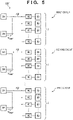
- Fig. 5 shows an example of the configuration of a print element substrate SB' according to an example of this embodiment.
- the plurality of memory elements ME and the plurality of write units 22 are divided into i groups, like the plurality of print elements PE. That is, j memory elements ME and j write units 22 are arranged in each of the first to ith groups.
- One current supply unit 23 can be provided for each group, and one determination unit 24 can be provided for each group.
- the i current supply units 23 and the i determination units 24, which are provided in this way, are preferably arrayed in the widthwise direction.
- the result of each determination unit 24 is obtained as a bit signal for each group. For this reason, i bit signals are obtained in total, and these can be read out as bit data using, for example, i flip-flop circuits connected in series.
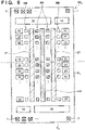
- Fig. 6 shows an example of the configuration of a print element substrate SB 2 according to the second embodiment.
- a current supply unit 23 and a determination unit 24 are juxtaposed in the widthwise direction on each of one side and the other side (the upper side and the lower side in Fig. 6 ) of short sides E S .
- a plurality of print elements PE, a plurality of memory elements ME, and a plurality of write units 22 are divided into the one side and the other side of the short sides E S . Note that this division is indicated by a broken line in Fig. 6 .
- the current supply unit 23 on the one side supplies a current. Based on a voltage Vm generated by this, the determination unit 24 on the one side determines the presence/absence of write to the memory elements ME. Similarly, to the memory elements ME on the other side of the short sides E S , the current supply unit 23 on the other side supplies a current. Based on the voltage Vm generated by this, the determination unit 24 on the other side determines the presence/absence of write to the memory elements ME.
- the current supply controller 233 may be provided only on the one side.
- the node between the high breakdown voltage transistor TR1 and the memory element ME is substantially in a floating state.
- Fig. 7 shows an example of the configuration of a print element substrate SB 3 according to the third embodiment.
- the print element substrate SB 3 further includes a resistive element R21 connected in parallel with each memory element ME. According to this configuration, it is possible to prevent write from being performed to the memory element ME in a case in which a high voltage is applied to the memory element ME via a write terminal Tx during the non-conductive state of a high breakdown voltage transistor TR1.
- An element substrate including a liquid discharge element comprising a memory element capable of storing individual information of the element substrate by write, the memory element being configured to change an impedance value by the write, a plurality of current supply elements capable of supplying a current to the memory element, and a determination unit configured to determine presence/absence of the write based on a voltage generated in the memory element by the current selectively supplied from the plurality of current supply elements, wherein the plurality of current supply elements constitute a part of a current mirror circuit and each supply the current in an amount according to a size ratio to the memory element.
Landscapes
- Semiconductor Memories (AREA)
- Particle Formation And Scattering Control In Inkjet Printers (AREA)
- Ink Jet (AREA)
Abstract
Description
- The present invention mainly relates to an element substrate.
- A liquid discharge head used in, for example, a printer using an inkjet printing method includes an element substrate on which a plurality of liquid discharge elements are arrayed (see
Japanese Patent Laid-Open No. 2014-58130 - In
Japanese Patent Laid-Open No. 2008-299989 - It is an exemplary object of the present invention to provide a technique advantageous in increasing the accuracy of determining the presence/absence of write to a memory element.
- The first aspect of the present invention provides an element substrate as specified in
claims 1 to 10. - The second aspect of the present invention provides a liquid discharge head as specified in
claim 11. - The third aspect of the present invention provides a liquid discharge apparatus as specified in
claim 12. - Further features of the present invention will become apparent from the following description of exemplary embodiments (with reference to the attached drawings).
-
-
Fig. 1 is a view showing an example of the configuration of a printing apparatus (liquid discharge apparatus); -
Fig. 2 is a view showing an example of the configuration of a print element substrate (element substrate); -
Fig. 3 is a view for explaining an example of a method of determining the presence/absence of write to a memory element; -
Fig. 4 is a sectional schematic view showing a part of the structure of the print element substrate; -
Fig. 5 is a view showing another example of the configuration of the print element substrate; -
Fig. 6 is a view showing still another example of the configuration of the print element substrate; and -
Fig. 7 is a view showing still another example of the configuration of the print element substrate. - Hereinafter, embodiments will be described in detail with reference to the attached drawings. Note, the following embodiments are not intended to limit the scope of the claimed invention. Multiple features are described in the embodiments, but limitation is not made to an invention that requires all such features, and multiple such features may be combined as appropriate. Furthermore, in the attached drawings, the same reference numerals are given to the same or similar configurations, and redundant description thereof is omitted.
- In this specification, embodiments will be described by exemplifying a printing apparatus using an inkjet printing method. However, the printing method is not limited to this. Also, the printing apparatus may be a single function printer having only a printing function or may be a multi-function printer having a plurality of functions such as a printing function, a FAX function, and a scanner function. In addition, the printing apparatus may be a manufacturing device configured to manufacture, for example, a color filter, an electronic device, an optical device, a microstructure, or the like using a predetermined printing method.
- Also, "print" in this specification should be interpreted in a broader sense. Hence, the mode of "print" is irrespective of whether or not the target to be formed on a print medium is significant information such as a character or graphic pattern, and is also irrespective of whether the target is manifested in a way that can be perceived visually by humans.
- "Print media" should also be interpreted in a broader sense, like "print". Hence, the concept of "print media" includes sheet-shaped members used in general, and any material capable of receiving ink, including paper, fabrics, plastic films, metals, glass, ceramics, resins, wood, and leathers can be used.
- "Ink" should also be interpreted in a broader sense, like "print". Hence, the concept of "ink" can include not only a liquid that is applied to a print medium to form an image, a design, a pattern, or the like but also an incidental liquid that can be provided to process a print medium or process ink (for example, coagulate or insolubilize color materials in ink applied to a print medium). Hence, in this specification, this can be expressed "liquid" in place of "ink".
- In these viewpoints, a printing apparatus may be referred to as a liquid discharge apparatus, a discharge apparatus, or the like. To the same effect, a printhead provided in the printing apparatus may be referred to as a liquid discharge head, a discharge head, or the like. Similarly, a print element substrate provided in the printhead may be referred to as a liquid discharge element substrate or a discharge element substrate, or simply as an element substrate. In addition, each of a plurality of print elements arrayed on the print element substrate may be referred to as a liquid discharge element, a discharge element, or the like.
-
Fig. 1 shows an example of the configuration of aprinting apparatus 1 according to the first embodiment. Theprinting apparatus 1 includes aprinthead 11 and adriver 12 and, in this embodiment, performs printing by an inkjet printing method. Theprinthead 11 is configured to execute printing on a predetermined print medium P, and includes a plurality of nozzles NZ and a print element substrate SB. Each nozzle NZ is a liquid discharge port that discharges a liquid received from a liquid tank TK that stores the liquid. The plurality of nozzles NZ are arrayed on a surface on a side to execute printing. - The print element substrate SB includes a plurality of print elements PE corresponding to the plurality of nozzles NZ. When each print element PE is driven, a liquid is discharged from the corresponding nozzle NZ, thereby executing printing. In this embodiment, a resistive element (or simply called a heater) that is an electrothermal transducer is used as the print element PE. As another embodiment, a piezoelectric element may be used.
- The
driver 12 includes aconveyance driver 121 and ahead driver 122. Theconveyance driver 121 conveys the print medium P set in the main body of theprinting apparatus 1 to theprinthead 11. Thehead driver 122 drives theprinthead 11 with respect to the conveyed print medium P to cause the individual nozzles NZ to discharge the liquid, thereby performing printing. - Note that in this embodiment, the
printhead 11 is a serial head that performs printing on the print medium P while scanning in a direction crossing the conveyance direction of the print medium P. As another embodiment, theprinthead 11 may be a line head capable of printing at once on the whole region of the print medium P in the widthwise direction. -
Fig. 2 shows an example of the configuration of the print element substrate SB. In a planar view (a viewpoint in a direction vertical to the principal plane, a top view), the print element substrate SB has an outer shape including a long side (first side) EL and a short side (second side) Es. In this embodiment, the print element substrate SB has a rectangular shape. As another embodiment, the print element substrate SB may have a square shape, a parallelogram shape, or a trapezoidal shape. In addition to the above-described plurality of print elements PE, the print element substrate SB includesdriving units 21, a plurality of memory elements ME, a plurality ofwrite units 22, acurrent supply unit 23, and adetermination unit 24. - In this embodiment, a channel LQ for a liquid is extended in a longitudinal direction (a direction parallel to the long side EL) in a planar view, and the plurality of print elements PE are arrayed in the longitudinal direction on both sides of the channel LQ. The driving
unit 21 is arranged, on each side of the channel LQ, between the long side EL and the plurality of print elements PE, and can individually drive the plurality of print elements PE. The liquid is supplied from the liquid tank TK to above the print element PE via the channel LQ, and after that, foamed and discharged when the drivingunits 21 drive the print elements PE. - Here, the driving
units 21 can drive the plurality of print elements PE by a time division method. That is, the plurality of print elements PE are divided into a plurality of groups, and the drivingunits 21 sequentially drive each of two or more print elements PE of each group as a block. For example, if the number of groups is i, and each group includes j print elements PE as blocks, first, the drivingunits 21 drive a first block (i print elements PE) for each of the first to ith groups. Next, the drivingunits 21 drive a second block (i print elements PE) for each of the first to ith groups. According to the same procedure, the drivingunits 21 sequentially drive a third, fourth,..., jth blocks (i print elements PE in each block) for each of the first to ith groups. - To implement driving of the plurality of print elements PE by the time division method, the driving
unit 21 can typically include a decoder, a shift register, a latch circuit, a selector, an AND circuit, an OR circuit, and the like. Note that each of i and j is an integer of 2 or more. Also, the group can also be called a time division group, and the block can also be called a time division block. - To correspond to the above-described plurality of print elements PE, the plurality of memory elements ME are arrayed in the longitudinal direction, and the plurality of
write units 22 are similarly arrayed in the longitudinal direction. Also, thecurrent supply unit 23 and thedetermination unit 24 are juxtaposed in the widthwise direction (a direction parallel to the short side Es). - In addition, at edge portions near the short sides ES of the print element substrate SB, a plurality of terminals T are arrayed in the widthwise direction. Supply of a power supply voltage to the print element substrate SB and signal transmission/reception of the print element substrate SB are performed via the plurality of terminals T. A power supply voltage VI shown in
Fig. 2 is 3.3 [V (volt)], and a power supply voltage V2 is 0 [V] (the voltage V2 can also be referred to as a ground voltage). Note that a voltage described in this specification represents a potential difference from the ground voltage V2. - To facilitate understanding,
Fig. 2 shows two types of voltages, that is, the voltages VI and V2. However, another power supply voltage different from the voltage VI and/or V2 may further be supplied to the print element substrate SB. This/these other voltages may be supplied to some of the circuit portions shown inFig. 2 in place of the voltage VI and/or V2. - The memory elements ME can store the individual information of the print element substrate SB, such as correction information for individual variations of the print element substrate SB, the number of printed sheets, the remaining ink amount, and whether to permit driving of the print elements PE. As the memory element ME, a so-called OTP memory (one time programmable memory) that permits write only once is used. In this embodiment, an anti-fuse element is used. Here, an anti-fuse element having a MOS (Metal Oxide Semiconductor) structure is used as the memory element ME.
- Each
write unit 22 is configured to implement one or more writes to the memory element ME, and includes a high breakdown voltage transistor TR1 and a control inverter circuit INV1. The high breakdown voltage transistor TR1 is connected in serial with the memory element ME As will be described later in detail, when brought into a conductive state, the high breakdown voltage transistor TR1 functions as a write transistor in write to the memory element ME, and also functions as a read transistor when confirming the presence/absence of write to the memory element ME. As the high breakdown voltage transistor TR1, a DMOS (Double Diffused MOS) transistor is used. - The control inverter circuit INV1 is connected to the gate terminal of the high breakdown voltage transistor TR1, and controls the high breakdown voltage transistor TR1 based on a control signal received via a node n1(set the high breakdown voltage transistor TR1 in a conductive state or a non-conductive state).
- Write to the memory element ME is done by applying a relatively high voltage (for example, 32 [V]) to the memory element ME via a write terminal Tx that is one of the plurality of terminals T during the conductive state of the high breakdown voltage transistor TR1 to cause dielectric breakdown of the MOS structure of the memory element ME. For this reason, the impedance value of the memory element ME can be changed by the write. In this embodiment, before write, the memory element ME is an insulated state, and exhibits a very large electric resistance value (or a high impedance of, for example, several [MΩ (megaohm)]). After write, the memory element ME is in a conductive state, and exhibits a relatively small electric resistance value (for example, several to several tens [kΩ (kiloohm)]. At the time of write, the high voltage is applied to the terminal Tx. Otherwise, the terminal Tx is in an open state.
- Note that as another embodiment, a fuse element may be used as the memory element ME In this case, before write, the memory element ME is in a short-circuited state, and exhibits a relatively small electric resistance value. After write, the memory element ME is in an open state, and exhibits a very large electric resistance value.
- The
current supply unit 23 includes acurrent generation unit 231, aselection unit 232, and acurrent supply controller 233. Thecurrent generation unit 231 includes a plurality of transistors MP10 to MP1K, and resistive elements R11 and R12. In this embodiment, p-channel MOS transistors are used as the transistors MPlo to MP1K. Note that K is an integer of 2 or more. - The transistors MP11 to MP1K constitute a current mirror circuit with the transistor MP10. For example, if the transistors MPlo to MP1K have the same channel length and channel widths different from each other, letting m be an arbitrary one of
integers 1 to K, a current according to the channel width ratio to the transistor MPlo flows to a transistor MP1m. Hence, each of the transistors MP11 to MP1K can output a current in an amount according to the size ratio. - In this embodiment, the resistive elements R11 and R12 are connected in series with the transistor MP10, and the voltage between the resistive elements R11 and R12 is used as a reference voltage VREF. Here, the resistive elements R11 and R12 are provided such that the reference voltage VREF = 1 [V] is obtained under the power supply voltage VI = 3.3 [V].
- The
selection unit 232 includes switch elements SW11 to SW1K corresponding to the transistors MP11 to MP1K, and can selectively connect the transistors MP11 to MP1K to the memory element ME For example, letting m be an arbitrary one ofintegers 1 to K, if a switch element SW1m is set in a conductive state, the transistor MP1m is connected to the memory element ME, and a current according to the size ratio is supplied to the memory element ME From this viewpoint, it can be said that each of the transistors MP11 to MP1K functions as a current supply element capable of supplying a current to the memory element ME - The
current supply controller 233 can individually control the switch elements SW11 to SW1K of theselection unit 232, thereby selectively setting the switch elements SW11 to SW1K in a conductive state. To facilitate understanding, in this embodiment, assume that one of the switch elements SW11 to SW1K is set in the conductive state by thecurrent supply controller 233, that is, one of the transistors MP11 to MP1K can selectively be connected to the memory element ME As another embodiment, two or more of the switch elements SW11 to SW1K may be set in the conductive state, that is, currents of two or more of the transistors MP11 to MP1K may be superimposed and supplied to the memory element ME Hence, thecurrent supply controller 233 need only be able to connect at least some of the transistors MP11 to MP1K to the memory element ME by theselection unit 232. - Summarizing the
current supply unit 23, thecurrent supply controller 233 outputs a control signal to the control inverter circuit INV1 via the node n1, thereby setting the high breakdown voltage transistor TR1 in the conductive state. During this, thecurrent supply controller 233 controls theselection unit 232, thereby supplying a desired amount of current from thecurrent generation unit 231 to the memory element ME via a node n2. - The
determination unit 24 is configured to determine the presence/absence of write to the memory element ME (that is, whether to permit driving of the print element PE). In this embodiment, thedetermination unit 24 is a comparator than compares a voltage (the voltage of the node n2) Vm generated in the memory element ME with the reference voltage VREF. Determination of thedetermination unit 24 is performed by supplying a current from the current supply unit 23 (one of the transistors MP11 to MP1K) to the memory element ME during the time when the control inverter circuit INV1 sets the high breakdown voltage transistor TR1 in the conductive state. In general, if the memory element ME is in a written state, the voltage Vm is lower than that in the state before the write to the memory element ME. Based on the magnitude relationship between the voltage Vm and the reference voltage VREF, the result of determination of thedetermination unit 24 is output from a node n3 to the circuit portion of the subsequent stage, or output from the terminal T of the print element substrate SB to the outside via the node n3. - In this way, the
determination unit 24 can determine the presence/absence of write to the memory element ME based on the voltage Vm generated in the memory element ME by the current supplied from thecurrent supply unit 23. If the memory element ME is in a written state, the drivingunit 21 considers that, for example, the corresponding print element PE cannot be driven, and suppresses driving of the corresponding print element PE. To complement this, the drivingunit 21 may alternatively drive another print element PE capable of recording almost the same position as the corresponding print element PE. - As will be described later in detail, the determination by the
determination unit 24 is performed to determine the presence/absence of write to the memory element ME, and can also be performed for another purpose, usage, or function. - As described above, the impedance value of the memory element ME can be changed by write. However, the impedance value may change depending on the conditions of the print element substrate SB. It is considered that the impedance value varies due to, for example, a peripheral environment such as a temperature, a manufacturing variation, a mode of dielectric breakdown of a MOS structure, and other factors. When the variations of the power supply voltage VI and the like are also taken into consideration, it is also considered that the amounts of currents output from the transistors MP10 to MP1K vary, and accordingly, the reference voltage VREF and the voltage Vm vary.
- For this reason, for example,
- (a) in a case in which in an evaluation step upon manufacturing the print element substrate SB, it is confirmed whether the MOS structure of the memory element ME is appropriately formed/it is confirmed whether the memory element ME is in a state before write (to be referred to as "manufacturing confirmation of the memory element ME" for the sake of discrimination),
- (b) in a case in which at another timing different from (a), it is specified not to permit driving of the print element PE, write to the corresponding memory element ME is performed, and after that, it is confirmed whether the write is appropriately implemented/it is confirmed whether the memory element ME is in a written state (to be referred to as "confirmation of write completion in the memory element ME" for the sake of discrimination), and
- (c) in a case in which at another timing different from (a) and (b), the presence/absence of write to the memory element ME is performed (to be referred to as "read from the memory element ME" for the sake of discrimination),
the conditions may be different from each other. As an example, when performing write to the memory element ME, a relatively large amount of current is supplied to the memory element ME, and it is therefore considered that the temperature of the print element substrate SB becomes high. - Hence, in the determination of the
determination unit 24, it is necessary to provide a margin that changes depending on several purposes, usages, or functions, and a current in an amount corresponding to these is preferably supplied to the memory element ME. - As described above, the memory element ME that is an anti-fuse element in this embodiment is in an insulated state and exhibits a very large electric resistance value before write, and is in a conductive state and exhibits a relatively small electric resistance value after write.
- Considering this, the
determination unit 24, for example: - preferably determines, in the case (a), whether the electric resistance value of the memory element ME is larger than R1M,
- preferably determines, in the case (b), whether the electric resistance value of the memory element ME is smaller than R1K (R1K < R1M), and
- preferably determines, in the case (c), whether the electric resistance value of the memory element ME is larger (or smaller) than R2K (R2K > R1K, R2K < R1M).
- The above-described matters occur because it is necessary to:
- reliably confirm that the memory element ME is in the state before write in the case (a),
- reliably confirm that the memory element ME is in the written state in the case (b), and
- prevent a determination error concerning the presence/absence of write to the memory element ME in the case (c).
- Note that as typical examples of parameters, the electric resistance value R1M is 100 [kΩ], the electric resistance value R1K is 5 [kΩ], and the electric resistance value R2K is 50 [kΩ]. However, the parameters are not limited to these values.
-
Fig. 3 shows the voltage Vm in a case in which K = 3 (a case in which a current is supplied from one of transistors MP11 to MP13 to the memory element ME). The abscissa represents the electric resistance value of the memory element ME The ordinate represents the voltage Vm generated in the memory element ME in correspondence with current amounts I11, I12, and I13 output from the transistors MP11, MP12, and MP13, respectively (I11 < I13 <I12). - Note that when reference voltage VREF = 1 [V] is set, as typical examples of parameters, the current amount I11 is 10 [µA (microampere)], the current amount I12 is 200 [µA], and the current amount I13 is 20 [µA]. However, the parameters are not limited to these values.
- According to this embodiment, as is apparent from
Fig. 3 , thedetermination unit 24 - can supply the current amount I11 from the transistor MP11 to the memory element ME and perform manufacturing confirmation of the memory element ME in the case (a),
- can supply the current amount I12 from the transistor MP12 to the memory element ME and perform confirmation of write completion in the memory element ME in the case (b), and
- can supply the current amount I13 from the transistor MP13 to the memory element ME and perform read from the memory element ME in the case (c).
- According to this configuration, in the case (c), a margin MG for determination is provided with respect to the cases (a) and (b). As compared to a case of K = 1, it is possible to appropriately prevent a determination error. The margin MG includes a margin for a determination error in both the written state and the state before write. In this embodiment, a case of K = 3 has been exemplified. As another embodiment, K = 2 is possible, and K ≥ 4 is also possible. The integer K can be changed in accordance with the purpose, usage, or function.
-
Fig. 4 is a sectional schematic view of a region including the memory element ME and the high breakdown voltage transistor TR1 on the print element substrate SB. For example, a plurality of p-type wells 41P and a plurality of n-type wells 41N, and p-type regions 42P and/or n-type regions 42N in the wells 41P or 41N are provided in a p-type semiconductor substrate 40. Between several regions 42P or 42N, LOCOS (Local Oxidation of Silicon) films are provided as thick insulating members OX. A gate electrode GT is provided such that a part thereof covers the insulating member OX. With this structure, a MOS structure serving as an anti-fuse element is formed as the memory element ME, and an n-channel DMOS transistor is formed as the high breakdown voltage transistor TR1. - Typically, silicon can be used for the above-described
semiconductor substrate 40, silicon oxide can be used for the insulating member OX, and polysilicon can be used for the gate electrode GT. The net p-type impurity concentration in thesemiconductor substrate 40 is, for example, about 1 × 10¹⁶ [cm-3]. The net p-type impurity concentration in the p-type well 41P is, for example, about 1 × 10¹⁸ [cm-3]. The net n-type impurity concentration in the n-type well 41N is, for example, about 1 × 10¹⁸ [cm-3]. The net p-type impurity concentration in the p-type region 42P is, for example, about 1 × 10¹⁹ [cm-3]. The net n-type impurity concentration in the n-type region 42N is, for example, about 1 × 10¹⁹ [cm-3]. Note that the net impurity concentrations are not limited to these examples. - As described above, according to this embodiment, the memory element ME is configured to store, by write, whether to permit driving of the print element PE and change the impedance value by the write. The transistors MP11 to MP1K constitute a part of a current mirror circuit, and each transistor supplies a current in an amount according to the size ratio to the memory element ME. The transistors MP11 to MP1K are provided in accordance with the purpose, usage, or function. In this embodiment, the current is selectively supplied from one of the transistors MP11 to MP1K to the memory element ME The
determination unit 24 determines the presence/absence of write to the memory element ME based on the voltage Vm generated in the memory element ME at that time. According to this configuration, it is possible to increase the accuracy of determination of thedetermination unit 24 independently of the variation of the impedance value of the memory element ME caused by a factor such as the peripheral environment or manufacturing variation, or the variations of the power supply voltage VI and the like. - Here, the single channel LQ has been exemplified, and a configuration in which the plurality of print elements PE, the driving
units 21, the plurality of memory elements ME, and the plurality ofwrite units 22 are arranged on both sides of the channel LQ has been described. The number of channels LQ may be two or more. In this case, the plurality of print elements PE, the drivingunits 21, the plurality of memory elements ME, and the plurality ofwrite units 22 are preferably arranged on both sides of each channel LQ. - The two or more channels LQ are assumed to be juxtaposed in the widthwise direction. However, these may additionally/alternatively be juxtaposed in the longitudinal direction. Note that in accordance with the number of channels LQ juxtaposed in the widthwise direction, the relationship between the long sides EL and the short sides ES in the outer shape of the print element substrate SB may be reversed.
- As described above, since the plurality of print elements PE are driven by the time division method, the plurality of memory elements ME and the plurality of
write units 22 may be managed on a group basis. -
Fig. 5 shows an example of the configuration of a print element substrate SB' according to an example of this embodiment. According to the print element substrate SB', the plurality of memory elements ME and the plurality ofwrite units 22 are divided into i groups, like the plurality of print elements PE. That is, j memory elements ME and j writeunits 22 are arranged in each of the first to ith groups. Onecurrent supply unit 23 can be provided for each group, and onedetermination unit 24 can be provided for each group. - The i
current supply units 23 and thei determination units 24, which are provided in this way, are preferably arrayed in the widthwise direction. The result of eachdetermination unit 24 is obtained as a bit signal for each group. For this reason, i bit signals are obtained in total, and these can be read out as bit data using, for example, i flip-flop circuits connected in series. - According to this configuration, it is advantageous in speeding up the determination of the presence/absence of write to the memory element ME by the
determination unit 24. Also, since the influence of a manufacturing variation can further be reduced, it is also advantageous in further speeding up the determination of thedetermination unit 24. - In the above-described first embodiment, a configuration in which the
current supply unit 23 and thedetermination unit 24 are juxtaposed in the widthwise direction on one of the two short sides Es has been exemplified. However, these may be installed on both of the two short sides ES. -
Fig. 6 shows an example of the configuration of a print element substrate SB2 according to the second embodiment. According to this embodiment, acurrent supply unit 23 and adetermination unit 24 are juxtaposed in the widthwise direction on each of one side and the other side (the upper side and the lower side inFig. 6 ) of short sides ES. To cope with this configuration, a plurality of print elements PE, a plurality of memory elements ME, and a plurality ofwrite units 22 are divided into the one side and the other side of the short sides ES. Note that this division is indicated by a broken line inFig. 6 . - To the memory elements ME on one side of the short sides ES, the
current supply unit 23 on the one side supplies a current. Based on a voltage Vm generated by this, thedetermination unit 24 on the one side determines the presence/absence of write to the memory elements ME. Similarly, to the memory elements ME on the other side of the short sides ES, thecurrent supply unit 23 on the other side supplies a current. Based on the voltage Vm generated by this, thedetermination unit 24 on the other side determines the presence/absence of write to the memory elements ME. - Note that in the pair of
current supply units 23, of acurrent generation unit 231, aselection unit 232, and acurrent supply controller 233, thecurrent supply controller 233 may be provided only on the one side. - According to this embodiment, since the influence of a manufacturing variation can further be reduced, it is more advantageous in further speeding up the determination of the
determination unit 24. - According to the configuration of the above-described first embodiment (see
Fig. 2 ), while the high breakdown voltage transistor TR1 is in the non-conductive state, the node between the high breakdown voltage transistor TR1 and the memory element ME is substantially in a floating state. Hence, if a high voltage is applied to the memory element ME via the write terminal Tx during the time, an unexpected dielectric breakdown may occur in the MOS structure of the memory element ME -
Fig. 7 shows an example of the configuration of a print element substrate SB3 according to the third embodiment. In this embodiment, the print element substrate SB3 further includes a resistive element R21 connected in parallel with each memory element ME. According to this configuration, it is possible to prevent write from being performed to the memory element ME in a case in which a high voltage is applied to the memory element ME via a write terminal Tx during the non-conductive state of a high breakdown voltage transistor TR1. - That is, according to this embodiment, it is possible to prevent erroneous write to the memory element ME. Hence, according to this embodiment, it is advantageous in improving the reliability of the print element substrate SB3 as well.
- While the present invention has been described with reference to exemplary embodiments, it is to be understood that the invention is not limited to the disclosed exemplary embodiments. The scope of the following claims is to be accorded the broadest interpretation so as to encompass all such modifications and equivalent structures and functions.
- An element substrate including a liquid discharge element, comprising a memory element capable of storing individual information of the element substrate by write, the memory element being configured to change an impedance value by the write, a plurality of current supply elements capable of supplying a current to the memory element, and a determination unit configured to determine presence/absence of the write based on a voltage generated in the memory element by the current selectively supplied from the plurality of current supply elements, wherein the plurality of current supply elements constitute a part of a current mirror circuit and each supply the current in an amount according to a size ratio to the memory element.
Claims (12)
- An element substrate including a liquid discharge element, characterized by comprising:a memory element capable of storing individual information of the element substrate by write, the memory element being configured to change an impedance value by the write;a plurality of current supply elements capable of supplying a current to the memory element; anda determination unit configured to determine presence/absence of the write based on a voltage generated in the memory element by the current selectively supplied from the plurality of current supply elements,wherein the plurality of current supply elements constitute a part of a current mirror circuit and each supply the current in an amount according to a size ratio to the memory element.
- The substrate according to claim 1, further comprising a selection unit configured to select one of the plurality of current supply elements, which is to be connected to the memory element.
- The substrate according to claim 1 or 2, wherein the determination unit is a comparator configured to compare the voltage generated in the memory element by the current supplied from at least one of the plurality of current supply elements with a reference voltage.
- The substrate according to any one of claims 1 to 3, further comprising a driving unit configured to drive the liquid discharge element,
wherein the driving unit suppresses the driving of the liquid discharge element if the determination unit determines that the memory element is in a written state. - The substrate according to any one of claims 1 to 4, wherein the memory element is an anti-fuse element.
- The substrate according to any one of claims 1 to 5, further comprising a resistive element connected in parallel with the memory element.
- The substrate according to any one of claims 1 to 6, further comprising a write transistor configured to perform write to the memory element.
- The substrate according to claim 7, wherein the write transistor is a DMOS transistor.
- The substrate according to claim 7 or 8, whereinthe liquid discharge element is one of a plurality of liquid discharge elements,the memory element is one of a plurality of memory elements corresponding to the plurality of liquid discharge elements,the write transistor is one of a plurality of transistors corresponding to the plurality of memory elements, andthe plurality of current supply elements supply the current to the memory element corresponding to, of the plurality of transistors, a transistor in a conductive state.
- The substrate according to claim 9, whereinthe element substrate has an outer shape including a first side and a second side in a planar view,the plurality of liquid discharge elements, the plurality of memory elements, and the plurality of transistors are arrayed in a direction parallel to the first side, andthe determination unit and the current mirror circuit are juxtaposed in a direction parallel to the second side.
- A liquid discharge head, comprising:an element substrate defined in any one of claims 1 to 10; anda liquid discharge port corresponding to a liquid discharge element.
- A liquid discharge apparatus, comprising:a liquid discharge head defined in claim 11; anda driver configured to drive the liquid discharge head.
Applications Claiming Priority (1)
| Application Number | Priority Date | Filing Date | Title |
|---|---|---|---|
| JP2021026638A JP7579173B2 (en) | 2021-02-22 | 2021-02-22 | Element substrate, liquid ejection head and liquid ejection device |
Publications (1)
| Publication Number | Publication Date |
|---|---|
| EP4046801A1 true EP4046801A1 (en) | 2022-08-24 |
Family
ID=80218411
Family Applications (1)
| Application Number | Title | Priority Date | Filing Date |
|---|---|---|---|
| EP22155129.4A Pending EP4046801A1 (en) | 2021-02-22 | 2022-02-04 | Element substrate, liquid discharge head, and liquid discharge apparatus |
Country Status (6)
| Country | Link |
|---|---|
| US (1) | US11975536B2 (en) |
| EP (1) | EP4046801A1 (en) |
| JP (1) | JP7579173B2 (en) |
| KR (1) | KR102876963B1 (en) |
| CN (1) | CN114953737A (en) |
| BR (1) | BR102022002530A2 (en) |
Families Citing this family (1)
| Publication number | Priority date | Publication date | Assignee | Title |
|---|---|---|---|---|
| JP2024166106A (en) * | 2023-05-16 | 2024-11-28 | 研能科技股▲ふん▼有限公司 | Inkjet head chip identification circuit |
Citations (4)
| Publication number | Priority date | Publication date | Assignee | Title |
|---|---|---|---|---|
| JPH08263994A (en) * | 1995-03-23 | 1996-10-11 | Kawasaki Steel Corp | Programmable read only memory |
| JP2008299989A (en) | 2007-06-01 | 2008-12-11 | Elpida Memory Inc | Antifuse replacement determination circuit and antifuse replacement determination method for semiconductor memory device |
| JP2014058130A (en) | 2012-09-18 | 2014-04-03 | Canon Inc | Substrate for recording head and recording device |
| US10894403B2 (en) * | 2017-03-30 | 2021-01-19 | Canon Kabushiki Kaisha | Semiconductor apparatus, liquid discharge head substrate, liquid discharge head, and liquid discharge apparatus |
Family Cites Families (9)
| Publication number | Priority date | Publication date | Assignee | Title |
|---|---|---|---|---|
| AUPN232495A0 (en) * | 1995-04-12 | 1995-05-04 | Eastman Kodak Company | Integrated fault tolerance in printing mechanisms |
| US5668751A (en) * | 1996-08-01 | 1997-09-16 | Micron Technology, Inc. | Antifuse programming method and apparatus |
| JP4933057B2 (en) * | 2005-05-13 | 2012-05-16 | キヤノン株式会社 | Head substrate, recording head, and recording apparatus |
| US7333383B2 (en) | 2005-08-23 | 2008-02-19 | Infineon Technologies Ag | Fuse resistance read-out circuit |
| JP5121439B2 (en) * | 2007-12-26 | 2013-01-16 | 株式会社東芝 | Nonvolatile semiconductor memory device |
| US9938136B2 (en) * | 2016-08-18 | 2018-04-10 | Stmicroelectronics Asia Pacific Pte Ltd | Fluid ejection device |
| JP6789729B2 (en) * | 2016-08-31 | 2020-11-25 | キヤノン株式会社 | Semiconductor devices, liquid discharge head substrates, liquid discharge heads, and liquid discharge devices |
| JP6843649B2 (en) * | 2017-02-22 | 2021-03-17 | キヤノン株式会社 | Recording element substrate, liquid discharge head and recording device |
| WO2018186852A1 (en) * | 2017-04-05 | 2018-10-11 | Hewlett-Packard Development Company, L.P. | On-die actuator failure detection |
-
2021
- 2021-02-22 JP JP2021026638A patent/JP7579173B2/en active Active
-
2022
- 2022-02-04 EP EP22155129.4A patent/EP4046801A1/en active Pending
- 2022-02-10 BR BR102022002530-4A patent/BR102022002530A2/en unknown
- 2022-02-11 US US17/670,325 patent/US11975536B2/en active Active
- 2022-02-21 KR KR1020220022371A patent/KR102876963B1/en active Active
- 2022-02-22 CN CN202210159396.9A patent/CN114953737A/en active Pending
Patent Citations (4)
| Publication number | Priority date | Publication date | Assignee | Title |
|---|---|---|---|---|
| JPH08263994A (en) * | 1995-03-23 | 1996-10-11 | Kawasaki Steel Corp | Programmable read only memory |
| JP2008299989A (en) | 2007-06-01 | 2008-12-11 | Elpida Memory Inc | Antifuse replacement determination circuit and antifuse replacement determination method for semiconductor memory device |
| JP2014058130A (en) | 2012-09-18 | 2014-04-03 | Canon Inc | Substrate for recording head and recording device |
| US10894403B2 (en) * | 2017-03-30 | 2021-01-19 | Canon Kabushiki Kaisha | Semiconductor apparatus, liquid discharge head substrate, liquid discharge head, and liquid discharge apparatus |
Also Published As
| Publication number | Publication date |
|---|---|
| US20220266590A1 (en) | 2022-08-25 |
| KR102876963B1 (en) | 2025-10-27 |
| KR20220120499A (en) | 2022-08-30 |
| JP7579173B2 (en) | 2024-11-07 |
| CN114953737A (en) | 2022-08-30 |
| JP2022128224A (en) | 2022-09-01 |
| US11975536B2 (en) | 2024-05-07 |
| BR102022002530A2 (en) | 2022-09-20 |
Similar Documents
| Publication | Publication Date | Title |
|---|---|---|
| JP5981815B2 (en) | Printhead substrate and printing apparatus | |
| US10894403B2 (en) | Semiconductor apparatus, liquid discharge head substrate, liquid discharge head, and liquid discharge apparatus | |
| US20220126576A1 (en) | Recording element substrate, liquid ejection head and recording apparatus | |
| US10566069B2 (en) | Semiconductor apparatus, liquid discharge head substrate, liquid discharge head, and liquid discharge apparatus | |
| EP4046801A1 (en) | Element substrate, liquid discharge head, and liquid discharge apparatus | |
| US10434772B2 (en) | Printhead and printing apparatus | |
| KR101659148B1 (en) | Element substrate, printhead, and printing apparatus | |
| US11837301B2 (en) | Substrate, printing apparatus, and manufacturing method | |
| US11981129B2 (en) | Element substrate, liquid discharge head, and printing apparatus | |
| US20230317186A1 (en) | Storage apparatus, liquid discharge head, and liquid discharge apparatus | |
| US20250077136A1 (en) | Printing apparatus and control method of printing apparatus | |
| US10532565B2 (en) | Print element substrate, printhead, and printing apparatus | |
| CN114083900A (en) | Printing element substrate, printhead, and printing apparatus | |
| US12374414B2 (en) | Semiconductor device, liquid discharge head, and liquid discharge apparatus | |
| JP6470858B2 (en) | Substrate, liquid discharge head, and liquid discharge apparatus | |
| US12036798B2 (en) | Control device and method for controlling element substrate | |
| JP6302513B2 (en) | Printhead substrate and printing apparatus | |
| US20050097385A1 (en) | Method of fault correction for an array of fusible links |
Legal Events
| Date | Code | Title | Description |
|---|---|---|---|
| PUAI | Public reference made under article 153(3) epc to a published international application that has entered the european phase |
Free format text: ORIGINAL CODE: 0009012 |
|
| STAA | Information on the status of an ep patent application or granted ep patent |
Free format text: STATUS: THE APPLICATION HAS BEEN PUBLISHED |
|
| AK | Designated contracting states |
Kind code of ref document: A1 Designated state(s): AL AT BE BG CH CY CZ DE DK EE ES FI FR GB GR HR HU IE IS IT LI LT LU LV MC MK MT NL NO PL PT RO RS SE SI SK SM TR |
|
| STAA | Information on the status of an ep patent application or granted ep patent |
Free format text: STATUS: REQUEST FOR EXAMINATION WAS MADE |
|
| 17P | Request for examination filed |
Effective date: 20230224 |
|
| RBV | Designated contracting states (corrected) |
Designated state(s): AL AT BE BG CH CY CZ DE DK EE ES FI FR GB GR HR HU IE IS IT LI LT LU LV MC MK MT NL NO PL PT RO RS SE SI SK SM TR |
|
| STAA | Information on the status of an ep patent application or granted ep patent |
Free format text: STATUS: EXAMINATION IS IN PROGRESS |
|
| 17Q | First examination report despatched |
Effective date: 20240422 |