EP4044438A1 - Multi-path digitation based on input signal fidelity and output requirements - Google Patents
Multi-path digitation based on input signal fidelity and output requirements Download PDFInfo
- Publication number
- EP4044438A1 EP4044438A1 EP22167235.5A EP22167235A EP4044438A1 EP 4044438 A1 EP4044438 A1 EP 4044438A1 EP 22167235 A EP22167235 A EP 22167235A EP 4044438 A1 EP4044438 A1 EP 4044438A1
- Authority
- EP
- European Patent Office
- Prior art keywords
- signal
- digital
- processing
- analog
- input signal
- Prior art date
- Legal status (The legal status is an assumption and is not a legal conclusion. Google has not performed a legal analysis and makes no representation as to the accuracy of the status listed.)
- Withdrawn
Links
Images


Classifications
-
- H—ELECTRICITY
- H03—ELECTRONIC CIRCUITRY
- H03M—CODING; DECODING; CODE CONVERSION IN GENERAL
- H03M1/00—Analogue/digital conversion; Digital/analogue conversion
- H03M1/12—Analogue/digital converters
- H03M1/1205—Multiplexed conversion systems
- H03M1/122—Shared using a single converter or a part thereof for multiple channels, e.g. a residue amplifier for multiple stages
-
- H—ELECTRICITY
- H03—ELECTRONIC CIRCUITRY
- H03M—CODING; DECODING; CODE CONVERSION IN GENERAL
- H03M1/00—Analogue/digital conversion; Digital/analogue conversion
- H03M1/12—Analogue/digital converters
- H03M1/18—Automatic control for modifying the range of signals the converter can handle, e.g. gain ranging
- H03M1/188—Multi-path, i.e. having a separate analogue/digital converter for each possible range
-
- G—PHYSICS
- G06—COMPUTING OR CALCULATING; COUNTING
- G06F—ELECTRIC DIGITAL DATA PROCESSING
- G06F1/00—Details not covered by groups G06F3/00 - G06F13/00 and G06F21/00
- G06F1/26—Power supply means, e.g. regulation thereof
- G06F1/32—Means for saving power
- G06F1/3203—Power management, i.e. event-based initiation of a power-saving mode
- G06F1/3234—Power saving characterised by the action undertaken
-
- G—PHYSICS
- G06—COMPUTING OR CALCULATING; COUNTING
- G06F—ELECTRIC DIGITAL DATA PROCESSING
- G06F1/00—Details not covered by groups G06F3/00 - G06F13/00 and G06F21/00
- G06F1/26—Power supply means, e.g. regulation thereof
- G06F1/266—Arrangements to supply power to external peripherals either directly from the computer or under computer control, e.g. supply of power through the communication port, computer controlled power-strips
-
- H—ELECTRICITY
- H03—ELECTRONIC CIRCUITRY
- H03M—CODING; DECODING; CODE CONVERSION IN GENERAL
- H03M1/00—Analogue/digital conversion; Digital/analogue conversion
- H03M1/002—Provisions or arrangements for saving power, e.g. by allowing a sleep mode, using lower supply voltage for downstream stages, using multiple clock domains or by selectively turning on stages when needed
-
- H—ELECTRICITY
- H03—ELECTRONIC CIRCUITRY
- H03M—CODING; DECODING; CODE CONVERSION IN GENERAL
- H03M1/00—Analogue/digital conversion; Digital/analogue conversion
- H03M1/12—Analogue/digital converters
-
- H—ELECTRICITY
- H04—ELECTRIC COMMUNICATION TECHNIQUE
- H04R—LOUDSPEAKERS, MICROPHONES, GRAMOPHONE PICK-UPS OR LIKE ACOUSTIC ELECTROMECHANICAL TRANSDUCERS; ELECTRIC HEARING AIDS; PUBLIC ADDRESS SYSTEMS
- H04R3/00—Circuits for transducers
- H04R3/04—Circuits for transducers for correcting frequency response
-
- G—PHYSICS
- G06—COMPUTING OR CALCULATING; COUNTING
- G06F—ELECTRIC DIGITAL DATA PROCESSING
- G06F1/00—Details not covered by groups G06F3/00 - G06F13/00 and G06F21/00
- G06F1/26—Power supply means, e.g. regulation thereof
- G06F1/32—Means for saving power
- G06F1/3203—Power management, i.e. event-based initiation of a power-saving mode
Definitions
- multipath ADCs/AFEs An example application for multipath ADCs/AFEs is use of them in a circuit for an audio system application, such as an audio mixing board or in a digital microphone system. Such an example application is disclosed in the Jahne patent.
- a tradeoff may exist between allowing larger signal swing (e.g., to allow swing of a signal between larger scale amplitudes) and low noise.
- the multipath ADCs/AFEs may provide high dynamic range signal digitization, with higher dynamic range for a given input power, and lower overall area than would be possible with conventional means.
- multipath ADCs/AFEs allow the overall circuit to burn less power, consume less area, and save on other such design costs.
- a processing system may include a plurality of processing paths and a controller.
- the plurality of processing paths may include a first processing path having a first analog gain and configured to generate a first digital signal based on an analog input signal and one or more other processing paths each having a respective second analog gain, each configured to consume a smaller amount of power than the first processing path, and each configured to generate a respective digital signal based on the analog input signal, wherein one of the one or more other processing paths has a noise floor based on fidelity characteristics of the analog input signal or subsequent processing requirements of a digital output signal generated from at least one of the first digital signal and the respective digital signals.
- the controller may be configured to select one of the first digital signal and the respective digital signals as the digital output signal of the processing system based on a magnitude of the analog input signal.
- a processing system may include a plurality of processing paths and a controller.
- the plurality of processing paths may include a first processing path having a first analog gain and configured to generate a first digital signal based on an analog input signal, a second processing path having a second analog gain and configured to generate a second digital signal based on the analog input signal, and a third processing path having a third analog gain, configured to consume a smaller amount of power than the first processing path and the second processing path, and configured to generate a third digital signal based on the analog input signal, wherein the third processing path has a noise floor based on fidelity characteristics of the analog input signal or subsequent processing requirements of a digital output signal generated from at least one of the first digital signal, the second digital signal, and the third digital signal.
- the controller may be configured to select one of the first digital signal, the second digital signal, and the third digital signal as the digital output signal of the processing system based on a magnitude of the analog input signal.
- a method may include processing an analog input signal with a first processing path having a first analog gain to generate a first digital signal based on the analog input signal, processing the analog input signal with one or more other processing paths each having a respective second analog gain, each configured to consume a smaller amount of power than the first processing path, and each configured to generate a respective digital signal based on the analog input signal, wherein one of the one or more other processing paths has a noise floor based on fidelity characteristics of the analog input signal or subsequent processing requirements of a digital output signal generated from at least one of the first digital signal and the respective digital signals, and selecting one of the first digital signal and the respective digital signals as the digital output signal of the processing system based on a magnitude of the analog input signal.
- a method may include processing an analog input signal with a first processing path having a first analog gain to generate a first digital signal based on the analog input signal, processing the analog input signal with a second processing path having a second analog gain to generate a second digital signal based on the analog input signal, processing the analog input signal with a third processing path having a third analog gain, configured to consume a smaller amount of power than the first processing path and the second processing path, and configured to generate a third digital signal based on the analog input signal, wherein the third processing path has a noise floor based on fidelity characteristics of the analog input signal or subsequent processing requirements of a digital output signal generated from at least one of the first digital signal, the second digital signal, and the third digital signal, and selecting one of the first digital signal, the second digital signal, and the third digital signal as the digital output signal of the processing system based on a magnitude of the analog input signal.
- FIGURE 1 illustrates a block diagram of selected components of an example signal processing system 100, in accordance with embodiments of the present disclosure.
- signal processing system 100 may include an analog signal source 101, an integrated circuit (IC) 105, and a digital processor 109.
- Analog signal source 101 may comprise any system, device, or apparatus configured to generate an analog electrical signal, for example an analog input signal ANALOG_IN.
- analog signal source 101 may comprise a microphone transducer.
- Integrated circuit 105 may comprise any suitable system, device, or apparatus configured to process analog input signal ANALOG_IN to generate a digital output signal DIGITAL_OUT and condition digital output signal DIGITAL_OUT for transmission over a bus to digital processor 109. Once converted to digital output signal DIGITAL_OUT, the signal may be transmitted over significantly longer distances without being susceptible to noise as compared to an analog transmission over the same distance.
- integrated circuit 105 may be disposed in close proximity with analog signal source 101 to ensure that the length of the analog line between analog signal source 101 and integrated circuit 105 is relatively short to minimize the amount of noise that can be picked up on an analog output line carrying analog input signal ANALOG_IN.
- analog signal source 101 and integrated circuit 105 may be formed on the same substrate. In other embodiments, analog signal source 101 and integrated circuit 105 may be formed on different substrates packaged within the same integrated circuit package.
- Digital processor 109 may comprise any suitable system, device, or apparatus configured to process digital output signal DIGITAL_OUT for use in a digital system.
- digital processor 109 may comprise a microprocessor, microcontroller, digital signal processor (DSP), application specific integrated circuit (ASIC), or any other device configured to interpret and/or execute program instructions and/or process data, such as digital output signal DIGITAL_OUT.
- DSP digital signal processor
- ASIC application specific integrated circuit
- FIGURE 2 illustrates a block diagram of selected components of integrated circuit 105, in accordance with embodiments of the present disclosure.
- integrated circuit 105 may include two or more processing paths 201a and 201b (which may be referred to herein individually as a processing path 201 and collectively as processing paths 201), each processing path 201 including a respective AFE 203 (e.g., AFE 203a, AFE 203b) and a respective ADC (e.g., ADC 215a, ADC 215b).
- AFE 203 e.g., AFE 203a, AFE 203b
- ADC e.g., ADC 215a, ADC 215b
- An AFE 203 may receive analog input signal ANALOG_IN via one or more input lines which may allow for receipt of a single-ended signal, differential signal, or any other suitable analog signal format and may comprise any suitable system, device, or apparatus configured to condition analog input signal ANALOG_IN for processing by ADC 215. Selected components for example embodiments of AFEs 203a and 203b are discussed in greater detail below with respect to FIGURE 3 .
- the output of each AFE 203 may be communicated to a respective ADC 215 on one or more output lines.
- An ADC 215 may comprise any suitable system, device, or apparatus configured to convert an analog signal received at its input, to a digital signal representative of analog input signal ANALOG_IN.
- ADC 215 may itself include one or more components (e.g., delta-sigma modulator, decimator, etc.) for carrying out the functionality of ADC 215. Selected components for the example embodiments of ADCs 215a and 215b are discussed in greater detail below with respect to FIGURE 3 .
- Driver 219 may receive the digital signal DIGITAL_OUT output by ADC 215 and may comprise any suitable system, device, or apparatus configured to condition such digital signal (e.g., encoding into Audio Engineering Society/European Broadcasting Union (AES/EBU), Sony/Philips Digital Interface Format (S/PDIF)), in the process generating digital output signal DIGITAL_OUT for transmission over a bus to digital audio processor 109.
- AES/EBU Audio Engineering Society/European Broadcasting Union
- S/PDIF Sony/Philips Digital Interface Format
- the bus receiving digital output signal DIGITAL_OUT is shown as single-ended.
- driver 219 may generate a differential digital output signal 107.
- Controller 220 may comprise any suitable system, device, or apparatus for selecting one of the digital signals output by the various processing paths 201 as digital output signal DIGITAL_OUT. In some embodiments, controller 220 may make such selection based on a magnitude of analog input signal ANALOG_IN or a signal derivative thereof, fidelity characteristics of analog input signal ANALOG_IN, and/or subsequent processing requirements of a digital output signal DIGITAL_OUT
- controller 220 may include an overload detector 221 that may determine whether or not a signal derivative of analog input signal ANALOG_IN (e.g., an output of a modulator 316a of delta-sigma modulator 308a, as shown in greater detail in FIGURE 3 ) is likely to cause clipping or other distortion of digital output signal DIGITAL_OUT if a particular processing path (e.g., processing path 201a) is selected.
- a signal derivative of analog input signal ANALOG_IN e.g., an output of a modulator 316a of delta-sigma modulator 308a, as
- processing path 201a may be a path adapted for low amplitudes of analog input signal ANALOG_IN and may thus have a high signal gain
- processing path 201b may be a path adapted for higher amplitudes of analog input signal ANALOG_IN and may thus have a lower signal gain.
- overload detector 221 may detect such condition, and cause state machine 225 to generate a control signal to select the digital signal generated by processing path 201b as digital output signal DIGITAL_OUT.
- controller 220 may include a level detector 223 that may detect an amplitude of analog input signal ANALOG_IN or a signal derivative thereof (e.g., a signal generated within ADC 215b) and communicate a signal indicative of such amplitude to state machine 225. Responsive to the signal received from level detector 223, state machine 225 may generate the control signal communicated to multiplexer 227.
- a level detector 223 may detect an amplitude of analog input signal ANALOG_IN or a signal derivative thereof (e.g., a signal generated within ADC 215b) and communicate a signal indicative of such amplitude to state machine 225. Responsive to the signal received from level detector 223, state machine 225 may generate the control signal communicated to multiplexer 227.
- analog input signal ANALOG_IN decreases from a relatively high amplitude to a lower amplitude, it may cross a threshold amplitude level whereby controller 220 may change the selection of digital output signal DIGITAL_OUT from the digital signal generated by processing path 201b (which may be adapted for higher amplitudes of analog input signal ANALOG_IN) to the digital signal generated by processing path 201a (which may be adapted for lower amplitudes of analog input signal ANALOG IN).
- a threshold amplitude level whereby controller 220 may change the selection of digital output signal DIGITAL_OUT from the digital signal generated by processing path 201b to the digital signal generated by processing path 201a may be lower than another threshold amplitude level whereby controller 220 may change the selection of digital output signal DIGITAL_OUT from the digital signal generated by processing path 201a to the digital signal generated by processing path 201b, in order to provide for hysteresis so that multiplexer 227 does not repeatedly switch between the paths.
- controller 220 may include an input signal analysis block 228 which may analyze or otherwise process a digital signal derived from analog input signal ANALOG_IN to determine fidelity characteristics of analog input signal ANALOG_IN and/or may include a downstream processing requirements block 230 which may receive or otherwise determine subsequent processing requirements of digital output signal DIGITAL_OUT.
- fidelity characteristics may include one or more of an acoustic noise floor of analog input signal ANALOG_IN, acoustic distortion of analog input signal ANALOG IN, a bandwidth of analog input signal ANALOG IN, and an intrinsic noise floor of at least one of the processing paths 201.
- controller 220 may determine that processing analog input signal ANALOG_IN with higher performance/higher power in processing paths 201 may not result in significant benefit over lower-power processing.
- state machine 225 may select the digital signal generated by processing path 201b as digital output signal DIGITAL_OUT and output one or more power control signals to components of processing path 201b in order to reduce power consumption of processing path 201b.
- Any suitable approach may be used to reduce power consumption of processing path 201b, including without limitation reduction of bias voltages or currents, modification of signal input impedances, modification of component bandwidths, selective powering of portions of amplifiers, and/or any other suitable analog power saving technique.
- processing path 201b may have a noise floor based on the fidelity characteristics of analog input signal ANALOG_IN or subsequent processing requirements of digital output signal DIGITAL_OUT.
- such one or more power control signals may power down processing path 201a to further reduce power, and processing path 201a may be powered up in response to controller 220 selecting the digital signal generated by processing path 201a as digital output signal DIGITAL_OUT.
- FIGURE 3 illustrates a block diagram of selected components of integrated circuit 105 depicting selected components of example embodiments of AFEs 203 and ADCs 215, in accordance with embodiments of the present disclosure.
- analog front end 203a of processing path 201a may include a high-pass filter 302 configured to high-pass filter analog input signal ANALOG_IN to remove direct current offsets or biases, which are often particularly troublesome for high-gain amplifiers, and output such filtered signal to a non-inverting amplifier 304.
- Non-inverting amplifier 304 may amplify analog input signal ANALOG IN by a non-inverting gain and communicate such amplified analog signal to ADC 215a.
- analog front end 203b of processing path 201b may include an inverting amplifier 306 which may amplify analog input signal ANALOG_IN by an inverting gain and communicate such amplified analog signal to ADC 215b.
- inverting amplifier 306 may be configured to apply a multiplicative gain of less than unity to analog input signal ANALOG_IN. By attenuating higher-amplitude signals, a greater dynamic range for analog input signal ANALOG_IN may be achieved, in spite of conventional wisdom that would generally dictate that signal loss should be avoided in a low-noise system.
- inverting amplifier 306 may receive the output of high-pass filter 302 instead of the unfiltered analog input signal ANALOG_IN.
- each of processing paths 201 may have approximately the same cumulative gain.
- ADC 215a or ADC 215b simply applying a digital gain with a negative sign in either of ADC 215a or ADC 215b will negate the opposite polarities of the gains of AFEs 203.
- each ADC 215 may include a respective delta-sigma modulator 308 (e.g., delta-sigma modulators 308a and 308b), a respective digital gain element 310 (e.g., digital gain elements 310a and 310b), and respective high-pass filters 312 (e.g., high-pass filters 312a and 312b).
- Each delta-sigma modulator 308 may be configured to modulate an analog signal into a corresponding digital signal.
- each delta-sigma modulator 308 may include a respective modulator 316 (e.g., modulators 316a, 316b) and a decimator 318 (e.g., decimators 318a, 318b).
- Each digital gain element 310 may apply a gain to a digital signal generated by its associated delta-sigma modulator 308.
- Each high-pass filter 312 may high-pass filter a digital signal generated by its associated digital gain element, to filter out any direct-current offsets present in the digital signal.
- High-pass filter 312b may also compensate for high-pass filter 302 present in AFE 203a.
- ADC 215a may comprise a latency matching element 314 to match any signal latencies between processing path 201a and processing path 201b
- ADC 215b may comprise a phase matching element 317 to account for any phase offset between processing path 201a and processing path 201b.
- phase matching element 317 may dynamically compensate for any phase mismatch between processing paths 201a and 201b by varying a delay of at least one of processing path 201a and processing path 201b.
- phase matching element 317 may comprise a high-pass filter.
- a magnitude of a gain of non-inverting amplifier 304 may be substantially larger than (e.g., significantly more than manufacturing tolerances, one or more orders of magnitude) a magnitude of a gain of inverting amplifier 306.
- a magnitude of digital gain element 310b may be substantially larger than (e.g., significantly more than manufacturing tolerances, one or more orders of magnitude) a magnitude of a gain of digital gain element 310a.
- a first path gain equal to the product of the magnitude of the gain of inverting amplifier 306 and the magnitude of a gain of digital gain element 310b may be substantially equal (e.g., within manufacturing tolerances) to a second path gain equal to the product of the magnitude of gain of non-inverting amplifier 304 and the gain of digital gain element 310a.
- the inverting gain of inverting amplifier 306 may be approximately -6 decibels
- the non-inverting gain of non-inverting amplifier 304 may be approximately 20 decibels
- the gain of digital gain element 310a may be approximately -26 decibels
- the gain of digital gain element 310b may be approximately 0 decibels.
- each processing path 201 may be adapted to process a particular amplitude of analog input signal ANALOG_IN.
- AFE 203a may be suited to process lower signal amplitudes, as non-inverting amplifier 304 may have a practically infinite input resistance, may have a relatively low level of input-referred noise as compared to inverting amplifier 306, and its larger gain may permit effective processing of smaller signals, but characteristics of AFE 203a may not be amenable to higher amplitudes.
- the high input resistance of non-inverting amplifier 304 may facilitate the use of a smaller capacitor area for high-pass filter 302 (as compared to traditional approaches for implementing high-pass filters) and thus may permit integration of circuitry of high-pass filter 302 into the same integrated circuit as non-inverting amplifier 304, inverting amplifier 306, ADC 215a, and/or ADC 215b.
- the ability to integrate circuitry into a single integrated circuit may allow for centralized control of the stimuli for switching between processing paths 201 by controller 220, and may allow for more direct timing control of the actual switching and transitioning between processing paths 201.
- level detector 223 may receive an output of delta-sigma modulator 308b as an input signal, rather than receiving an output of ADC 215b.
- AFE 203b may be suited to process higher signal amplitudes, as its lower gain will reduce the likelihood of signal clipping, and may provide for greater dynamic range for analog input signal ANALOG_IN as compared to traditional approaches.
- first path gain and the second path gain may be unequal. If switching between paths occurs when such path gains are unequal, signal artifacts may occur due to an instantaneous, discontinuous change in magnitude of the digital output signal between two gain levels. For example, in audio signals, such artifacts may include human-perceptible "pops" or "clicks" in acoustic sounds generated from audio signals.
- controller 220 may program an additional gain into one or both of processing paths 201 to compensate for differences in the first path gain and second path gain.
- This additional gain factor may equalize the first path gain and the second path gain.
- controller 220 may determine a scale factor indicative of the magnitude of difference (e.g., whether an intentional difference or unintentional mismatch) between the first path gain of processing path 201a and the second path gain of processing path 201b.
- the controller may determine the first path gain and the second path gain by comparing the digital output signals of each processing path to analog input signal ANALOG_IN or a derivative thereof. If such digital output signals have been filtered by a high-pass filter (e.g., high-pass filters 312), a direct-current offset between the signals may be effectively filtered out, which may be necessary to accurately compute the relative path gains. Controller 220 may determine the scale factor by calculating one of a root mean square average of the first path gain and the second path gain and a least mean squares estimate of the difference between the first path gain and the second path gain.
- a high-pass filter e.g., high-pass filters 312
- controller 220 may program an additional gain into one of processing paths 201 to compensate for the gain difference indicated by the scale factor. For example, controller 220 may calibrate one or both of the first path gain and the second path gain by applying a gain equal to the scale factor or the reciprocal of the gain factor (e.g., 1/gain factor), as appropriate. Such scaling may be performed by modifying one or both of digital gains 310. In some embodiments, controller 220 may apply the additional gain to the processing path 201 of the digital signal not selected as digital output signal DIGITAL_OUT.
- controller 220 may apply the additional gain to processing path 201a when the digital signal of ADC 215b is selected as digital output signal DIGITAL_OUT and apply the additional gain to processing path 201b when the digital signal of ADC 215a is selected as digital output signal DIGITAL_OUT.
- the additional gain once applied to a path gain of a processing path 201, may be allowed over a period of time to approach or "leak" to a factor of 1, in order to constrain the additional gain and compensate for any cumulative (e.g., over multiple switching events between digital signals of ADCs 215) bias in the calculation of the additional gain.
- multiple switching events between paths may cause the gain factor to increase or decrease in an unconstrained manner as such additional gain, if different than unity, affects the outputs of the multiple paths and thus affects the calculation of the scaling factor.
- switching selection of digital output signal DIGITAL_OUT from the digital signal of ADC 215a to the digital signal of ADC 215b (or vice versa), may occur substantially immediately.
- controller 220 and multiplexer 227 may be configured to transition, continuously or in steps, digital output signal DIGITAL_OUT from a first digital signal to a second digital signal such that during such transition, digital output signal DIGITAL_OUT is a weighted average of the first digital signal and the second digital signal wherein a weight of the second digital signal relative to a weight of the first digital signal increases during the transition.
- controller 220 and/or multiplexer 227 weighs digital signals output by ADCs 215 as follows:
- controller 220 and/or multiplexer 227 weighs digital signals output by ADCs 215 as follows:
- a transition in digital output signal DIGITAL_OUT (either continuously or in steps) from the digital signal of ADC 215a to the digital signal of ADC 215b (or vice versa) may occur over a defined maximum duration of time.
- a rate of transition may be based on a magnitude of analog input signal ANALOG IN (e.g., the rate of transition may be faster at lower amplitudes and slower at higher amplitudes).
- the minimum rate of such transition may be limited such that the transition occurs over a defined maximum duration of time, wherein the maximum duration of time is independent of the magnitude of the analog input signal.
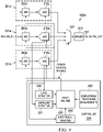
- FIGURE 4 illustrates a block diagram of selected components of another integrated circuit 105A for processing an analog signal to generate a digital signal, in accordance with embodiments of the present disclosure.
- integrated circuit 105 depicted in FIGURE 1 may be implemented using integrated circuit 105A.
- Integrated circuit 105A may be similar in many respects to integrated circuit 105 depicted in FIGURE 2 . Accordingly, only the major differences between integrated circuit 105A and integrated circuit 105 are discussed below.
- integrated circuit 105A may include a third processing path 201c in addition to processing paths 201a and 201b.
- processing path 201c may have an AFE 203c which may be similar to either of AFE 203a or AFE 203b, and an ADC 215c which may be similar to either of ADC 215a or ADC 215b.
- AFC 203c may have an analog gain which is smaller than one or both of the respective analog gains of AFE 203a and AFE 203b.
- processing path 201c and its various components may be configured to consume a smaller amount of power than that of processing paths 201a and 201b.
- input signal analysis block 228 may analyze or otherwise process a digital signal derived from analog input signal ANALOG_IN to determine fidelity characteristics of analog input signal ANALOG_IN and/or downstream processing requirements block 230 may receive or otherwise determine subsequent processing requirements of digital output signal DIGITAL_OUT.
- fidelity characteristics may include one or more of an acoustic noise floor of analog input signal ANALOG IN, acoustic distortion of analog input signal ANALOG IN, a bandwidth of analog input signal ANALOG IN, and an intrinsic noise floor of at least one of processing path 201a and processing path 201b.
- controller 220 may determine that processing analog input signal ANALOG_IN with higher performance/higher power processing paths 201a or 201b may not result in significant benefit over the lower-power processing of processing path 201c.
- state machine 225 may select the digital signal generated by processing path 201c as digital output signal DIGITAL_OUT.
- state machine 225 may in such cases output one or more power control signals to components of processing path 201c in order to control power consumption of processing path 201c.
- Any suitable approach may be used to control power consumption of processing path 201c, including without limitation control of bias voltages or currents, control of signal input impedances, control of component bandwidths, selective powering of portions of amplifiers, and/or any other suitable analog power control technique.
- processing path 201c may have a noise floor based on the fidelity characteristics of analog input signal ANALOG_IN or subsequent processing requirements of digital output signal DIGITAL_OUT.
- such one or more power control signals may power down processing path 201a and/or processing path 201b to further reduce power, and processing path 201a may be powered up in response to controller 220 selecting digital signal generated by processing path 201a as digital output signal DIGITAL_OUT while processing path 201b may be powered up in response to controller 220 selecting digital signal generated by processing path 201b as digital output signal DIGITAL_OUT.
- power consumption in a signal processing system may be dynamically optimized by optimizing performance of the processing system based on fidelity characteristics of the signal to be processed and/or subsequent processing requirements for the processed signal. For example, a lower power, lower performance processing path may have a higher noise floor by virtue of the lower power consumption. However, in certain cases, such poorer noise floor (or signal-to-noise ratio) may be adequate given fidelity characteristics of the signal to be processed and/or subsequent processing requirements for the processed signal when higher performance processing and the lower intrinsic noise floor of the higher performance processing path might be of little advantage in processing the signal.
Landscapes
- Engineering & Computer Science (AREA)
- Theoretical Computer Science (AREA)
- Physics & Mathematics (AREA)
- General Engineering & Computer Science (AREA)
- General Physics & Mathematics (AREA)
- Computer Hardware Design (AREA)
- Acoustics & Sound (AREA)
- Signal Processing (AREA)
- Amplifiers (AREA)
- Analogue/Digital Conversion (AREA)
- Noise Elimination (AREA)
Abstract
Description
- The present disclosure relates in general to signal processing systems, and more particularly, to multiple path signal processing systems.
- The use of multipath analog-to-digital converters (ADCs) and analog front ends (AFEs) (e.g., two or more path ADCs/AFEs) in electrical circuits is known. Example multipath ADCs and AFEs and use of them in multiple electrical circuit paths are disclosed in
U.S. Patent No. 5,714,956 entitled "Process and System for the Analog-to-Digital Conversion of Signals" to Jahne et al. ("Jahne patent"),U.S. Patent No. 5,600,317 entitled "Apparatus for the Conversion of Analog Audio Signals to a Digital Data Stream" to Knoth et al. ("Knoth patent") andU.S. Patent No. 6,271,780 entitled "Gain Ranging Analog-to-Digital Converter with Error Correction" to Gong et al. ("Gong patent"). The use of multipath circuits may reduce noise as one path may be optimized for processing small amplitude signals (e.g., for processing low noise signals) while another circuit path with another set of ADC and AFE is optimized for large amplitude signals (e.g., allowing for higher dynamic range). - An example application for multipath ADCs/AFEs is use of them in a circuit for an audio system application, such as an audio mixing board or in a digital microphone system. Such an example application is disclosed in the Jahne patent. In designing a circuit with multipath ADCs/AFEs that are used in respective multiple circuit paths, a tradeoff may exist between allowing larger signal swing (e.g., to allow swing of a signal between larger scale amplitudes) and low noise. Furthermore, the multipath ADCs/AFEs may provide high dynamic range signal digitization, with higher dynamic range for a given input power, and lower overall area than would be possible with conventional means. In other words, by allowing a separate optimization for each type of signal (e.g., large and small signals) that is provided each respective path, multipath ADCs/AFEs allow the overall circuit to burn less power, consume less area, and save on other such design costs.
- In accordance with the teachings of the present disclosure, certain disadvantages and problems associated with implementation of a multiple AFE/ADC path may be reduced or eliminated.
- In accordance with embodiments of the present disclosure, a processing system may include a plurality of processing paths and a controller. The plurality of processing paths may include a first processing path having a first analog gain and configured to generate a first digital signal based on an analog input signal and one or more other processing paths each having a respective second analog gain, each configured to consume a smaller amount of power than the first processing path, and each configured to generate a respective digital signal based on the analog input signal, wherein one of the one or more other processing paths has a noise floor based on fidelity characteristics of the analog input signal or subsequent processing requirements of a digital output signal generated from at least one of the first digital signal and the respective digital signals. The controller may be configured to select one of the first digital signal and the respective digital signals as the digital output signal of the processing system based on a magnitude of the analog input signal.
- In accordance with these and other embodiments of the present disclosure, a processing system may include a plurality of processing paths and a controller. The plurality of processing paths may include a first processing path having a first analog gain and configured to generate a first digital signal based on an analog input signal, a second processing path having a second analog gain and configured to generate a second digital signal based on the analog input signal, and a third processing path having a third analog gain, configured to consume a smaller amount of power than the first processing path and the second processing path, and configured to generate a third digital signal based on the analog input signal, wherein the third processing path has a noise floor based on fidelity characteristics of the analog input signal or subsequent processing requirements of a digital output signal generated from at least one of the first digital signal, the second digital signal, and the third digital signal. The controller may be configured to select one of the first digital signal, the second digital signal, and the third digital signal as the digital output signal of the processing system based on a magnitude of the analog input signal.
- In accordance with these and other embodiments of the present disclosure, a method may include processing an analog input signal with a first processing path having a first analog gain to generate a first digital signal based on the analog input signal, processing the analog input signal with one or more other processing paths each having a respective second analog gain, each configured to consume a smaller amount of power than the first processing path, and each configured to generate a respective digital signal based on the analog input signal, wherein one of the one or more other processing paths has a noise floor based on fidelity characteristics of the analog input signal or subsequent processing requirements of a digital output signal generated from at least one of the first digital signal and the respective digital signals, and selecting one of the first digital signal and the respective digital signals as the digital output signal of the processing system based on a magnitude of the analog input signal.
- In accordance with these and other embodiments of the present disclosure, a method may include processing an analog input signal with a first processing path having a first analog gain to generate a first digital signal based on the analog input signal, processing the analog input signal with a second processing path having a second analog gain to generate a second digital signal based on the analog input signal, processing the analog input signal with a third processing path having a third analog gain, configured to consume a smaller amount of power than the first processing path and the second processing path, and configured to generate a third digital signal based on the analog input signal, wherein the third processing path has a noise floor based on fidelity characteristics of the analog input signal or subsequent processing requirements of a digital output signal generated from at least one of the first digital signal, the second digital signal, and the third digital signal, and selecting one of the first digital signal, the second digital signal, and the third digital signal as the digital output signal of the processing system based on a magnitude of the analog input signal.
- Technical advantages of the present disclosure may be readily apparent to one having ordinary skill in the art from the figures, description and claims included herein. The objects and advantages of the embodiments will be realized and achieved at least by the elements, features, and combinations particularly pointed out in the claims.
- It is to be understood that both the foregoing general description and the following detailed description are explanatory examples and are not restrictive of the claims set forth in this disclosure.
- A more complete understanding of the present embodiments and advantages thereof may be acquired by referring to the following description taken in conjunction with the accompanying drawings, in which like reference numbers indicate like features, and wherein:
-
FIGURE 1 illustrates a block diagram of selected components of an example signal processing system, in accordance with embodiments of the present disclosure; -
FIGURE 2 illustrates a block diagram of selected components of an integrated circuit for processing an analog signal to generate a digital signal, in accordance with embodiments of the present disclosure; -
FIGURE 3 illustrates a block diagram of selected components of the integrated circuit ofFIGURE 2 depicting selected components of example embodiments of analog front ends and analog-to-digital converters, in accordance with embodiments of the present disclosure; and -
FIGURE 4 illustrates a block diagram of selected components of another integrated circuit for processing an analog signal to generate a digital signal, in accordance with embodiments of the present disclosure. -
FIGURE 1 illustrates a block diagram of selected components of an examplesignal processing system 100, in accordance with embodiments of the present disclosure. As shown inFIGURE 1 ,signal processing system 100 may include ananalog signal source 101, an integrated circuit (IC) 105, and adigital processor 109.Analog signal source 101 may comprise any system, device, or apparatus configured to generate an analog electrical signal, for example an analog input signal ANALOG_IN. For example, in embodiments in whichsignal processing system 100 is a processing system,analog signal source 101 may comprise a microphone transducer. -
Integrated circuit 105 may comprise any suitable system, device, or apparatus configured to process analog input signal ANALOG_IN to generate a digital output signal DIGITAL_OUT and condition digital output signal DIGITAL_OUT for transmission over a bus todigital processor 109. Once converted to digital output signal DIGITAL_OUT, the signal may be transmitted over significantly longer distances without being susceptible to noise as compared to an analog transmission over the same distance. In some embodiments,integrated circuit 105 may be disposed in close proximity withanalog signal source 101 to ensure that the length of the analog line betweenanalog signal source 101 andintegrated circuit 105 is relatively short to minimize the amount of noise that can be picked up on an analog output line carrying analog input signal ANALOG_IN. For example, in some embodiments,analog signal source 101 andintegrated circuit 105 may be formed on the same substrate. In other embodiments,analog signal source 101 andintegrated circuit 105 may be formed on different substrates packaged within the same integrated circuit package. -
Digital processor 109 may comprise any suitable system, device, or apparatus configured to process digital output signal DIGITAL_OUT for use in a digital system. For example,digital processor 109 may comprise a microprocessor, microcontroller, digital signal processor (DSP), application specific integrated circuit (ASIC), or any other device configured to interpret and/or execute program instructions and/or process data, such as digital output signal DIGITAL_OUT. -
Signal processing system 100 may be used in any application in which it is desired to process an analog signal to generate a digital signal. Thus, in some embodiments,signal processing system 100 may be integral to an audio device that converts analog signals (e.g., from a microphone) to digital signals representing the sound incident on a microphone. As another example,signal processing system 100 may be integral to a radio-frequency device (e.g., a mobile telephone) to convert radio-frequency analog signals into digital signals. -
FIGURE 2 illustrates a block diagram of selected components ofintegrated circuit 105, in accordance with embodiments of the present disclosure. As shown inFIGURE 2 ,integrated circuit 105 may include two ormore processing paths FIGURE 3 . The output of each AFE 203 may be communicated to a respective ADC 215 on one or more output lines. - An ADC 215 may comprise any suitable system, device, or apparatus configured to convert an analog signal received at its input, to a digital signal representative of analog input signal ANALOG_IN. ADC 215 may itself include one or more components (e.g., delta-sigma modulator, decimator, etc.) for carrying out the functionality of ADC 215. Selected components for the example embodiments of
ADCs FIGURE 3 . - A
multiplexer 227 may receive a respective digital signal from each of processing paths 201 and may select one of the digital signals as digital output signal DIGITAL_OUT based on a control signal generated by and communicated from acontroller 220. -
Driver 219 may receive the digital signal DIGITAL_OUT output by ADC 215 and may comprise any suitable system, device, or apparatus configured to condition such digital signal (e.g., encoding into Audio Engineering Society/European Broadcasting Union (AES/EBU), Sony/Philips Digital Interface Format (S/PDIF)), in the process generating digital output signal DIGITAL_OUT for transmission over a bus todigital audio processor 109. InFIGURE 2 , the bus receiving digital output signal DIGITAL_OUT is shown as single-ended. In some embodiments,driver 219 may generate a differentialdigital output signal 107. -
Controller 220 may comprise any suitable system, device, or apparatus for selecting one of the digital signals output by the various processing paths 201 as digital output signal DIGITAL_OUT. In some embodiments,controller 220 may make such selection based on a magnitude of analog input signal ANALOG_IN or a signal derivative thereof, fidelity characteristics of analog input signal ANALOG_IN, and/or subsequent processing requirements of a digital output signal DIGITAL_OUT For example,controller 220 may include anoverload detector 221 that may determine whether or not a signal derivative of analog input signal ANALOG_IN (e.g., an output of amodulator 316a of delta-sigma modulator 308a, as shown in greater detail inFIGURE 3 ) is likely to cause clipping or other distortion of digital output signal DIGITAL_OUT if a particular processing path (e.g.,processing path 201a) is selected. If clipping or other distortion of digital output signal DIGITAL_OUT is likely if the particular processing path (e.g.,processing path 201a) is selected,state machine 225 ofcontroller 220 may generate a control signal so that another processing path (e.g.,processing path 201b) is selected. To further illustrate, in some embodiments,processing path 201a may be a path adapted for low amplitudes of analog input signal ANALOG_IN and may thus have a high signal gain, whileprocessing path 201b may be a path adapted for higher amplitudes of analog input signal ANALOG_IN and may thus have a lower signal gain. Thus, if analog input signal ANALOG_IN or a derivative thereof is greater than a threshold value indicative of a condition whereby digital output signal DIGITAL_OUT may experience clipping or other distortion ifprocessing path 201a is selected,overload detector 221 may detect such condition, and causestate machine 225 to generate a control signal to select the digital signal generated byprocessing path 201b as digital output signal DIGITAL_OUT. - As another example,
controller 220 may include alevel detector 223 that may detect an amplitude of analog input signal ANALOG_IN or a signal derivative thereof (e.g., a signal generated withinADC 215b) and communicate a signal indicative of such amplitude tostate machine 225. Responsive to the signal received fromlevel detector 223,state machine 225 may generate the control signal communicated to multiplexer 227. To illustrate, as analog input signal ANALOG_IN decreases from a relatively high amplitude to a lower amplitude, it may cross a threshold amplitude level wherebycontroller 220 may change the selection of digital output signal DIGITAL_OUT from the digital signal generated byprocessing path 201b (which may be adapted for higher amplitudes of analog input signal ANALOG_IN) to the digital signal generated byprocessing path 201a (which may be adapted for lower amplitudes of analog input signal ANALOG IN). In some embodiments, a threshold amplitude level wherebycontroller 220 may change the selection of digital output signal DIGITAL_OUT from the digital signal generated by processingpath 201b to the digital signal generated by processingpath 201a may be lower than another threshold amplitude level wherebycontroller 220 may change the selection of digital output signal DIGITAL_OUT from the digital signal generated by processingpath 201a to the digital signal generated by processingpath 201b, in order to provide for hysteresis so thatmultiplexer 227 does not repeatedly switch between the paths. - As a further example,
controller 220 may include an inputsignal analysis block 228 which may analyze or otherwise process a digital signal derived from analog input signal ANALOG_IN to determine fidelity characteristics of analog input signal ANALOG_IN and/or may include a downstream processing requirements block 230 which may receive or otherwise determine subsequent processing requirements of digital output signal DIGITAL_OUT.Examples of such fidelity characteristics may include one or more of an acoustic noise floor of analog input signal ANALOG_IN, acoustic distortion of analog input signal ANALOG IN, a bandwidth of analog input signal ANALOG IN, and an intrinsic noise floor of at least one of the processing paths 201. Examples of such subsequent processing requirements comprise one or more of a bandwidth of a downstream process that receives digital output signal DIGITAL_OUT, a bit width of a downstream process that receives digital output signal DIGITAL_OUT, and a signal-to-noise ratio requirement of a downstream process that receives digital output signal DIGITAL_OUT. Based on such fidelity characteristics and/or downstream processing requirements,controller 220 may determine that processing analog input signal ANALOG_IN with higher performance/higher power in processing paths 201 may not result in significant benefit over lower-power processing. Accordingly, in such cases,state machine 225 may select the digital signal generated by processingpath 201b as digital output signal DIGITAL_OUT and output one or more power control signals to components ofprocessing path 201b in order to reduce power consumption ofprocessing path 201b. Any suitable approach may be used to reduce power consumption ofprocessing path 201b, including without limitation reduction of bias voltages or currents, modification of signal input impedances, modification of component bandwidths, selective powering of portions of amplifiers, and/or any other suitable analog power saving technique. By controlling power consumption ofprocessing path 201b, processingpath 201b may have a noise floor based on the fidelity characteristics of analog input signal ANALOG_IN or subsequent processing requirements of digital output signal DIGITAL_OUT. In some embodiments, such one or more power control signals may power down processingpath 201a to further reduce power, andprocessing path 201a may be powered up in response tocontroller 220 selecting the digital signal generated by processingpath 201a as digital output signal DIGITAL_OUT. -
FIGURE 3 illustrates a block diagram of selected components ofintegrated circuit 105 depicting selected components of example embodiments of AFEs 203 and ADCs 215, in accordance with embodiments of the present disclosure. As shown inFIGURE 3 , analogfront end 203a ofprocessing path 201a may include a high-pass filter 302 configured to high-pass filter analog input signal ANALOG_IN to remove direct current offsets or biases, which are often particularly troublesome for high-gain amplifiers, and output such filtered signal to anon-inverting amplifier 304.Non-inverting amplifier 304 may amplify analog input signal ANALOG IN by a non-inverting gain and communicate such amplified analog signal toADC 215a. In some embodiments, high-pass filter 302 may be formed on the same integrated circuit as one or more ofAFE 203a,AFE 203b,ADC 215a, andADC 215b. Because of the presence of high-pass filter 302 inprocessing path 201a, but not processingpath 201b, processing paths 201 may each have a different frequency response to analog input signal ANALOG_IN. - Also as shown in
FIGURE 3 , analogfront end 203b ofprocessing path 201b may include an invertingamplifier 306 which may amplify analog input signal ANALOG_IN by an inverting gain and communicate such amplified analog signal toADC 215b. In some embodiments, invertingamplifier 306 may be configured to apply a multiplicative gain of less than unity to analog input signal ANALOG_IN. By attenuating higher-amplitude signals, a greater dynamic range for analog input signal ANALOG_IN may be achieved, in spite of conventional wisdom that would generally dictate that signal loss should be avoided in a low-noise system. In these and other embodiments, although not depicted inFIGURE 3 , invertingamplifier 306 may receive the output of high-pass filter 302 instead of the unfiltered analog input signal ANALOG_IN. - Although
AFEs ADC 215a orADC 215b will negate the opposite polarities of the gains of AFEs 203. - As depicted in
FIGURE 3 , each ADC 215 may include a respective delta-sigma modulator 308 (e.g., delta-sigma modulators digital gain elements pass filters pass filter 312b may also compensate for high-pass filter 302 present inAFE 203a. - In addition,
ADC 215a may comprise alatency matching element 314 to match any signal latencies betweenprocessing path 201a andprocessing path 201b, whileADC 215b may comprise aphase matching element 317 to account for any phase offset betweenprocessing path 201a andprocessing path 201b. For example,phase matching element 317 may dynamically compensate for any phase mismatch betweenprocessing paths processing path 201a andprocessing path 201b. In some embodiments,phase matching element 317 may comprise a high-pass filter. - In some embodiments, a magnitude of a gain of
non-inverting amplifier 304 may be substantially larger than (e.g., significantly more than manufacturing tolerances, one or more orders of magnitude) a magnitude of a gain of invertingamplifier 306. In addition, in these and other embodiments, a magnitude ofdigital gain element 310b may be substantially larger than (e.g., significantly more than manufacturing tolerances, one or more orders of magnitude) a magnitude of a gain ofdigital gain element 310a. Consequently, in such embodiments, a first path gain equal to the product of the magnitude of the gain of invertingamplifier 306 and the magnitude of a gain ofdigital gain element 310b may be substantially equal (e.g., within manufacturing tolerances) to a second path gain equal to the product of the magnitude of gain ofnon-inverting amplifier 304 and the gain ofdigital gain element 310a. As a specific example, in some embodiments, the inverting gain of invertingamplifier 306 may be approximately -6 decibels, the non-inverting gain ofnon-inverting amplifier 304 may be approximately 20 decibels, the gain ofdigital gain element 310a may be approximately -26 decibels, and the gain ofdigital gain element 310b may be approximately 0 decibels. - Accordingly, each processing path 201 may be adapted to process a particular amplitude of analog input signal ANALOG_IN. For example,
AFE 203a may be suited to process lower signal amplitudes, asnon-inverting amplifier 304 may have a practically infinite input resistance, may have a relatively low level of input-referred noise as compared to invertingamplifier 306, and its larger gain may permit effective processing of smaller signals, but characteristics ofAFE 203a may not be amenable to higher amplitudes. The high input resistance ofnon-inverting amplifier 304 may facilitate the use of a smaller capacitor area for high-pass filter 302 (as compared to traditional approaches for implementing high-pass filters) and thus may permit integration of circuitry of high-pass filter 302 into the same integrated circuit asnon-inverting amplifier 304, invertingamplifier 306,ADC 215a, and/orADC 215b. In addition, the ability to integrate circuitry into a single integrated circuit may allow for centralized control of the stimuli for switching between processing paths 201 bycontroller 220, and may allow for more direct timing control of the actual switching and transitioning between processing paths 201. For example, because circuitry is integrated into a single integrated circuitry,level detector 223 may receive an output of delta-sigma modulator 308b as an input signal, rather than receiving an output ofADC 215b. - On the other hand,
AFE 203b may be suited to process higher signal amplitudes, as its lower gain will reduce the likelihood of signal clipping, and may provide for greater dynamic range for analog input signal ANALOG_IN as compared to traditional approaches. - Despite a designer's best efforts to match the first path gain and the second path gain, process variations, temperature variations, manufacturing tolerances, and/or other variations may lead to the first path gain and the second path gain being unequal. If switching between paths occurs when such path gains are unequal, signal artifacts may occur due to an instantaneous, discontinuous change in magnitude of the digital output signal between two gain levels. For example, in audio signals, such artifacts may include human-perceptible "pops" or "clicks" in acoustic sounds generated from audio signals.
- In some embodiments, in order to reduce or eliminate the occurrence of such artifacts when switching selection between the digital output signal of
ADC 215a and the digital output signal ofADC 215b, and vice versa,controller 220 may program an additional gain into one or both of processing paths 201 to compensate for differences in the first path gain and second path gain. This additional gain factor may equalize the first path gain and the second path gain. To illustrate,controller 220 may determine a scale factor indicative of the magnitude of difference (e.g., whether an intentional difference or unintentional mismatch) between the first path gain ofprocessing path 201a and the second path gain ofprocessing path 201b. The controller may determine the first path gain and the second path gain by comparing the digital output signals of each processing path to analog input signal ANALOG_IN or a derivative thereof. If such digital output signals have been filtered by a high-pass filter (e.g., high-pass filters 312), a direct-current offset between the signals may be effectively filtered out, which may be necessary to accurately compute the relative path gains.Controller 220 may determine the scale factor by calculating one of a root mean square average of the first path gain and the second path gain and a least mean squares estimate of the difference between the first path gain and the second path gain. Prior to switching selection between the first digital signal generated byADC 215a and the second digital signal generated byADC 215b (or vice versa),controller 220 may program an additional gain into one of processing paths 201 to compensate for the gain difference indicated by the scale factor. For example,controller 220 may calibrate one or both of the first path gain and the second path gain by applying a gain equal to the scale factor or the reciprocal of the gain factor (e.g., 1/gain factor), as appropriate. Such scaling may be performed by modifying one or both of digital gains 310. In some embodiments,controller 220 may apply the additional gain to the processing path 201 of the digital signal not selected as digital output signal DIGITAL_OUT. For example,controller 220 may apply the additional gain toprocessing path 201a when the digital signal ofADC 215b is selected as digital output signal DIGITAL_OUT and apply the additional gain toprocessing path 201b when the digital signal ofADC 215a is selected as digital output signal DIGITAL_OUT. - In some embodiments, the additional gain, once applied to a path gain of a processing path 201, may be allowed over a period of time to approach or "leak" to a factor of 1, in order to constrain the additional gain and compensate for any cumulative (e.g., over multiple switching events between digital signals of ADCs 215) bias in the calculation of the additional gain. Without undertaking this step to allow the additional gain to leak to unity, multiple switching events between paths may cause the gain factor to increase or decrease in an unconstrained manner as such additional gain, if different than unity, affects the outputs of the multiple paths and thus affects the calculation of the scaling factor.
- In some embodiments, switching selection of digital output signal DIGITAL_OUT from the digital signal of
ADC 215a to the digital signal ofADC 215b (or vice versa), may occur substantially immediately. However, in some embodiments, to reduce or eliminate artifacts from occurring when switching selection of digital output signal DIGITAL_OUT from the digital signal ofADC 215a to the digital signal ofADC 215b (or vice versa),controller 220 andmultiplexer 227 may be configured to transition, continuously or in steps, digital output signal DIGITAL_OUT from a first digital signal to a second digital signal such that during such transition, digital output signal DIGITAL_OUT is a weighted average of the first digital signal and the second digital signal wherein a weight of the second digital signal relative to a weight of the first digital signal increases during the transition. For example, if a transition is desired between digital signal ofADC 215a and digital signal ofADC 215b as digital output signal DIGITAL_OUT, such transition may be in steps, wherein in each step,controller 220 and/ormultiplexer 227 weighs digital signals output by ADCs 215 as follows: - 1) 100% digital signal of
ADC 215a and 0% digital signal ofADC 215b; - 2) 80% digital signal of
ADC 215a and 20% digital signal ofADC 215b; - 3) 60% digital signal of
ADC 215a and 40% digital signal ofADC 215b; - 4) 30% digital signal of
ADC 215a and 70% digital signal ofADC 215b; - 5) 10% digital signal of
ADC 215a and 90% digital signal ofADC 215b; and - 6) 0% digital signal of
ADC ADC 215b. - As another example, if a transition is desired between digital signal of
ADC 215b and digital signal ofADC 215a as digital output signal DIGITAL_OUT, such transition may be in steps, wherein in each step,controller 220 and/ormultiplexer 227 weighs digital signals output by ADCs 215 as follows: - 1) 100% digital signal of
ADC 215b and 0% digital signal ofADC 215a; - 2) 70% digital signal of
ADC 215b and 30% digital signal ofADC 215a; - 3) 60% digital signal of
ADC 215b and 40% digital signal ofADC 215a; - 4) 20% digital signal of
ADC 215b and 80% digital signal ofADC 215a; - 5) 5% digital signal of
ADC 215b and 95% digital signal ofADC 215a; and - 6) 0% digital signal of
ADC ADC 215a. - In some embodiments, a transition in digital output signal DIGITAL_OUT (either continuously or in steps) from the digital signal of
ADC 215a to the digital signal ofADC 215b (or vice versa) may occur over a defined maximum duration of time. In these and other embodiments, when transitioning (either continuously or in steps) digital output signal DIGITAL_OUT from the digital signal ofADC 215b to the digital signal ofADC 215a, a rate of transition may be based on a magnitude of analog input signal ANALOG IN (e.g., the rate of transition may be faster at lower amplitudes and slower at higher amplitudes). In such embodiments, the minimum rate of such transition may be limited such that the transition occurs over a defined maximum duration of time, wherein the maximum duration of time is independent of the magnitude of the analog input signal. -
FIGURE 4 illustrates a block diagram of selected components of anotherintegrated circuit 105A for processing an analog signal to generate a digital signal, in accordance with embodiments of the present disclosure. In some embodiments, integratedcircuit 105 depicted inFIGURE 1 may be implemented using integratedcircuit 105A.Integrated circuit 105A may be similar in many respects tointegrated circuit 105 depicted inFIGURE 2 . Accordingly, only the major differences betweenintegrated circuit 105A andintegrated circuit 105 are discussed below. As shown inFIGURE 4 , integratedcircuit 105A may include athird processing path 201c in addition toprocessing paths FIGURE 4 ,processing path 201c may have anAFE 203c which may be similar to either ofAFE 203a orAFE 203b, and anADC 215c which may be similar to either ofADC 215a orADC 215b. Inprocessing path 201c,AFC 203c may have an analog gain which is smaller than one or both of the respective analog gains ofAFE 203a andAFE 203b. In addition, processingpath 201c and its various components may be configured to consume a smaller amount of power than that ofprocessing paths - In operation, input
signal analysis block 228 may analyze or otherwise process a digital signal derived from analog input signal ANALOG_IN to determine fidelity characteristics of analog input signal ANALOG_IN and/or downstream processing requirements block 230 may receive or otherwise determine subsequent processing requirements of digital output signal DIGITAL_OUT. Examples of such fidelity characteristics may include one or more of an acoustic noise floor of analog input signal ANALOG IN, acoustic distortion of analog input signal ANALOG IN, a bandwidth of analog input signal ANALOG IN, and an intrinsic noise floor of at least one ofprocessing path 201a andprocessing path 201b. Examples of such subsequent processing requirements comprise one or more of a bandwidth of a downstream process that receives digital output signal DIGITAL_OUT, a bit width of a downstream process that receives digital output signal DIGITAL_OUT, and a signal-to-noise ratio requirement of a downstream process that receives digital output signal DIGITAL_OUT.Based on such fidelity characteristics and/or downstream processing requirements,controller 220 may determine that processing analog input signal ANALOG_IN with higher performance/higherpower processing paths processing path 201c. Accordingly, in such cases,state machine 225 may select the digital signal generated by processingpath 201c as digital output signal DIGITAL_OUT.In addition,state machine 225 may in such cases output one or more power control signals to components ofprocessing path 201c in order to control power consumption ofprocessing path 201c. Any suitable approach may be used to control power consumption ofprocessing path 201c, including without limitation control of bias voltages or currents, control of signal input impedances, control of component bandwidths, selective powering of portions of amplifiers, and/or any other suitable analog power control technique. By controlling power consumption ofprocessing path 201c, processingpath 201c may have a noise floor based on the fidelity characteristics of analog input signal ANALOG_IN or subsequent processing requirements of digital output signal DIGITAL_OUT. In some embodiments, such one or more power control signals may power down processingpath 201a and/orprocessing path 201b to further reduce power, andprocessing path 201a may be powered up in response tocontroller 220 selecting digital signal generated by processingpath 201a as digital output signal DIGITAL_OUT while processingpath 201b may be powered up in response tocontroller 220 selecting digital signal generated by processingpath 201b as digital output signal DIGITAL_OUT. - Using the systems and methods described herein, power consumption in a signal processing system may be dynamically optimized by optimizing performance of the processing system based on fidelity characteristics of the signal to be processed and/or subsequent processing requirements for the processed signal. For example, a lower power, lower performance processing path may have a higher noise floor by virtue of the lower power consumption. However, in certain cases, such poorer noise floor (or signal-to-noise ratio) may be adequate given fidelity characteristics of the signal to be processed and/or subsequent processing requirements for the processed signal when higher performance processing and the lower intrinsic noise floor of the higher performance processing path might be of little advantage in processing the signal.
- This disclosure encompasses all changes, substitutions, variations, alterations, and modifications to the example embodiments herein that a person having ordinary skill in the art would comprehend. Similarly, where appropriate, the appended claims encompass all changes, substitutions, variations, alterations, and modifications to the example embodiments herein that a person having ordinary skill in the art would comprehend. Moreover, reference in the appended claims to an apparatus or system or a component of an apparatus or system being adapted to, arranged to, capable of, configured to, enabled to, operable to, or operative to perform a particular function encompasses that apparatus, system, or component, whether or not it or that particular function is activated, turned on, or unlocked, as long as that apparatus, system, or component is so adapted, arranged, capable, configured, enabled, operable, or operative.
- All examples and conditional language recited herein are intended for pedagogical objects to aid the reader in understanding the disclosure and the concepts contributed by the inventor to furthering the art, and are construed as being without limitation to such specifically recited examples and conditions. Although embodiments of the present disclosure have been described in detail, it should be understood that various changes, substitutions, and alterations could be made hereto without departing from the spirit and scope of the disclosure.
- Various aspects of the disclosure will now be described by way of the following numbered statements:
- S1. A processing system comprising:
- a plurality of processing paths comprising:
- a first processing path having a first analog gain and configured to generate a first digital signal based on an analog input signal; and
- one or more other processing paths each having a respective second analog gain, each configured to consume a smaller amount of power than the first processing path, and each configured to generate a respective digital signal based on the analog input signal, wherein one of the one or more other processing paths has a noise floor based on fidelity characteristics of the analog input signal or subsequent processing requirements of a digital output signal generated from at least one of the first digital signal and the respective digital signals; and
- a controller configured to select one of the first digital signal and the respective digital signals as the digital output signal of the processing system based on a magnitude of the analog input signal.
- S2. The processing system of Statement S1, wherein the controller is further configured to:
- power down the first processing path when one of the respective digital signals of the one or more other processing paths is selected as the digital output signal; and
- power up the first processing path in response to selecting the first digital signal as the digital output signal.
- S3. The processing system of Statement S1, wherein the one or more other processing paths comprise:
- a second processing path; and
- a third processing path configured to consume a smaller amount of power than the second processing path.
- S4. The processing system of Statement S1, wherein the fidelity characteristics comprise at least one of an acoustic noise floor of the analog input signal, acoustic distortion of the analog input signal, a bandwidth of the analog input signal, and an intrinsic noise floor of at least one of the processing paths.
- S5. The processing system of Statement S1, wherein the subsequent processing requirements comprise at least one of a bandwidth of a downstream process that receives the digital output signal, a bit width of a downstream process that receives the digital output signal, and a signal-to-noise ratio requirement of a downstream process that receives the digital output signal.
- S6. The processing system of Statement S1, wherein the respective second analog gains are smaller than that of the first analog gain.
- S7. A processing system comprising:
a plurality of processing paths comprising:- a first processing path having a first analog gain and configured to generate a first digital signal based on an analog input signal;
- a second processing path having a second analog gain and configured to generate a second digital signal based on the analog input signal; and
- a third processing path having a third analog gain, configured to consume a smaller amount of power than the first processing path and the second processing path, and configured to generate a third digital signal based on the analog input signal, wherein the third processing path has a noise floor based on fidelity characteristics of the analog input signal or subsequent processing requirements of a digital output signal generated from at least one of the first digital signal, the second digital signal, and the third digital signal; and
- a controller configured to select one of the first digital signal, the second digital signal, and the third digital signal as the digital output signal of the processing system based on a magnitude of the analog input signal.
- S8. The processing system of Statement S7, wherein the controller is further configured to:
- power down at least the first processing path when the third digital signal is selected as the digital output signal; and
- power up at least the first processing path in response to selecting the first digital signal as the digital output signal.
- S9. The processing system of Statement S7, wherein the fidelity characteristics comprise at least one of an acoustic noise floor of the analog input signal, acoustic distortion of the analog input signal, a bandwidth of the analog input signal, and an intrinsic noise floor of at least one of the processing paths.
- S10. The processing system of Statement S7, wherein the subsequent processing requirements comprise at least one of a bandwidth of a downstream process that receives the digital output signal, a bit width of a downstream process that receives the digital output signal, and a signal-to-noise ratio requirement of a downstream process that receives the digital output signal.
- S11. The processing system of Statement S7, wherein the third analog gain is smaller than that of at least one of the first analog gain and the second analog gain.
- S12. A method comprising:
- processing an analog input signal with a first processing path having a first analog gain to generate a first digital signal based on the analog input signal;
- processing the analog input signal with one or more other processing paths each having a respective second analog gain, each configured to consume a smaller amount of power than the first processing path, and each configured to generate a respective digital signal based on the analog input signal, wherein one of the one or more other processing paths has a noise floor based on fidelity characteristics of the analog input signal or subsequent processing requirements of a digital output signal generated from at least one of the first digital signal and the respective digital signals; and
- selecting one of the first digital signal and the respective digital signals as the digital output signal of the processing system based on a magnitude of the analog input signal.
- S13. The method of Statement S12, controller is further comprising:
- powering down the first processing path when one of the respective digital signals of the one or more other processing paths is selected as the digital output signal; and
- powering up the first processing path in response to selecting the first digital signal as the digital output signal.
- S14. The method of Statement S12, wherein the one or more other processing paths comprise:
- a second processing path; and
- a third processing path configured to consume a smaller amount of power than the second processing path.
- S15. The method of Statement S12, wherein the fidelity characteristics comprise at least one of an acoustic noise floor of the analog input signal, acoustic distortion of the analog input signal, a bandwidth of the analog input signal, and an intrinsic noise floor of at least one of the processing paths.
- S16. The method of Statement S12, wherein the subsequent processing requirements comprise at least one of a bandwidth of a downstream process that receives the digital output signal, a bit width of a downstream process that receives the digital output signal, and a signal-to-noise ratio requirement of a downstream process that receives the digital output signal.
- S17. The method of Statement S12, wherein the respective second analog gains are smaller than that of the first analog gain.
- S18. A method comprising:
- processing an analog input signal with a first processing path having a first analog gain to generate a first digital signal based on the analog input signal;
- processing the analog input signal with a second processing path having a second analog gain to generate a second digital signal based on the analog input signal;
- processing the analog input signal with a third processing path having a third analog gain, configured to consume a smaller amount of power than the first processing path and the second processing path, and configured to generate a third digital signal based on the analog input signal, wherein the third processing path has a noise floor based on fidelity characteristics of the analog input signal or subsequent processing requirements of a digital output signal generated from at least one of the first digital signal, the second digital signal, and the third digital signal; and
- selecting one of the first digital signal, the second digital signal, and the third digital signal as the digital output signal of the processing system based on a magnitude of the analog input signal.
- S19. The method of Statement S18, wherein the controller is further configured to: power down at least the first processing path when the third digital signal is selected as the digital output signal; and
power up at least the first processing path in response to selecting the first digital signal as the digital output signal. - S20. The method of Statement S18, wherein the fidelity characteristics comprise at least one of an acoustic noise floor of the analog input signal, acoustic distortion of the analog input signal, a bandwidth of the analog input signal, and an intrinsic noise floor of at least one of the processing paths.
- S21. The method of Statement S18, wherein the subsequent processing requirements comprise at least one of a bandwidth of a downstream process that receives the digital output signal, a bit width of a downstream process that receives the digital output signal, and a signal-to-noise ratio requirement of a downstream process that receives the digital output signal.
- S22. The method of Statement S18, wherein the third analog gain is smaller than that of at least one of the first analog gain and the second analog gain.
Claims (12)
- A processing system comprising:a plurality of processing paths comprising:a first processing path having a first analog gain and configured to generate a first digital signal based on an analog input signal; andone or more other processing paths each having a respective second analog gain, each configured to consume a smaller amount of power than the first processing path, and each configured to generate a respective digital signal based on the analog input signal, wherein one of the one or more other processing paths has a noise floor based on fidelity characteristics of the analog input signal or subsequent processing requirements of a digital output signal generated from at least one of the first digital signal and the respective digital signals; anda controller configured to select one of the first digital signal and the respective digital signals as the digital output signal of the processing system based on a magnitude of the analog input signal in order to enable separate optimization for each type of signal that is provided in each of the plurality of processing paths.
- The processing system of Claim 1, wherein the controller is further configured to:power down the first processing path when one of the respective digital signals of the one or more other processing paths is selected as the digital output signal; andpower up the first processing path in response to selecting the first digital signal as the digital output signal.
- The processing system of Claim 1, wherein the one or more other processing paths comprise:a second processing path; anda third processing path configured to consume a smaller amount of power than the second processing path.
- The processing system of Claim 1, wherein the fidelity characteristics comprise at least one of an acoustic noise floor of the analog input signal, acoustic distortion of the analog input signal, a bandwidth of the analog input signal, and an intrinsic noise floor of at least one of the processing paths.
- The processing system of Claim 1, wherein the subsequent processing requirements comprise at least one of a bandwidth of a downstream process that receives the digital output signal, a bit width of a downstream process that receives the digital output signal, and a signal-to-noise ratio requirement of a downstream process that receives the digital output signal.
- The processing system of Claim 1, wherein the respective second analog gains are smaller than that of the first analog gain.
- A method comprising:processing an analog input signal with a first processing path having a first analog gain to generate a first digital signal based on the analog input signal;processing the analog input signal with one or more other processing paths each having a respective second analog gain, each configured to consume a smaller amount of power than the first processing path, and each configured to generate a respective digital signal based on the analog input signal, wherein one of the one or more other processing paths has a noise floor based on fidelity characteristics of the analog input signal or subsequent processing requirements of a digital output signal generated from at least one of the first digital signal and the respective digital signals; andselecting one of the first digital signal and the respective digital signals as the digital output signal of the processing system based on a magnitude of the analog input signal in order to enable separate optimization for each type of signal that is provided in each of the plurality of processing paths.
- The method of Claim 7, controller is further comprising:powering down the first processing path when one of the respective digital signals of the one or more other processing paths is selected as the digital output signal; andpowering up the first processing path in response to selecting the first digital signal as the digital output signal.
- The method of Claim 7, wherein the one or more other processing paths comprise:a second processing path; anda third processing path configured to consume a smaller amount of power than the second processing path.
- The method of Claim 7, wherein the fidelity characteristics comprise at least one of an acoustic noise floor of the analog input signal, acoustic distortion of the analog input signal, a bandwidth of the analog input signal, and an intrinsic noise floor of at least one of the processing paths.
- The method of Claim 7, wherein the subsequent processing requirements comprise at least one of a bandwidth of a downstream process that receives the digital output signal, a bit width of a downstream process that receives the digital output signal, and a signal-to-noise ratio requirement of a downstream process that receives the digital output signal.
- The method of Claim 7, wherein the respective second analog gains are smaller than that of the first analog gain.
Applications Claiming Priority (3)
| Application Number | Priority Date | Filing Date | Title |
|---|---|---|---|
| US15/233,624 US10545561B2 (en) | 2016-08-10 | 2016-08-10 | Multi-path digitation based on input signal fidelity and output requirements |
| EP17754567.0A EP3497789A1 (en) | 2016-08-10 | 2017-08-08 | Multi-path digitation based on input signal fidelity and output requirements |
| PCT/US2017/045861 WO2018031525A1 (en) | 2016-08-10 | 2017-08-08 | Multi-path digitation based on input signal fidelity and output requirements |
Related Parent Applications (1)
| Application Number | Title | Priority Date | Filing Date |
|---|---|---|---|
| EP17754567.0A Division EP3497789A1 (en) | 2016-08-10 | 2017-08-08 | Multi-path digitation based on input signal fidelity and output requirements |
Publications (1)
| Publication Number | Publication Date |
|---|---|
| EP4044438A1 true EP4044438A1 (en) | 2022-08-17 |
Family
ID=59010914
Family Applications (2)
| Application Number | Title | Priority Date | Filing Date |
|---|---|---|---|
| EP22167235.5A Withdrawn EP4044438A1 (en) | 2016-08-10 | 2017-08-08 | Multi-path digitation based on input signal fidelity and output requirements |
| EP17754567.0A Ceased EP3497789A1 (en) | 2016-08-10 | 2017-08-08 | Multi-path digitation based on input signal fidelity and output requirements |
Family Applications After (1)
| Application Number | Title | Priority Date | Filing Date |
|---|---|---|---|
| EP17754567.0A Ceased EP3497789A1 (en) | 2016-08-10 | 2017-08-08 | Multi-path digitation based on input signal fidelity and output requirements |
Country Status (6)
| Country | Link |
|---|---|
| US (1) | US10545561B2 (en) |
| EP (2) | EP4044438A1 (en) |
| KR (1) | KR102260032B1 (en) |
| CN (1) | CN109661778B (en) |
| GB (1) | GB2552867A (en) |
| WO (1) | WO2018031525A1 (en) |
Families Citing this family (9)
| Publication number | Priority date | Publication date | Assignee | Title |
|---|---|---|---|---|
| US10284217B1 (en) | 2014-03-05 | 2019-05-07 | Cirrus Logic, Inc. | Multi-path analog front end and analog-to-digital converter for a signal processing system |
| US10545561B2 (en) | 2016-08-10 | 2020-01-28 | Cirrus Logic, Inc. | Multi-path digitation based on input signal fidelity and output requirements |
| US10263630B2 (en) | 2016-08-11 | 2019-04-16 | Cirrus Logic, Inc. | Multi-path analog front end with adaptive path |
| US9929703B1 (en) | 2016-09-27 | 2018-03-27 | Cirrus Logic, Inc. | Amplifier with configurable final output stage |
| US10509659B1 (en) * | 2016-09-28 | 2019-12-17 | Amazon Technologies, Inc. | Input processing logic to produce outputs for downstream systems using configurations |
| US10956369B1 (en) | 2017-04-06 | 2021-03-23 | Amazon Technologies, Inc. | Data aggregations in a distributed environment |
| US10321230B2 (en) | 2017-04-07 | 2019-06-11 | Cirrus Logic, Inc. | Switching in an audio system with multiple playback paths |
| CN111082805B (en) * | 2019-12-31 | 2023-08-11 | 南京英锐创电子科技有限公司 | Analog front end and control method thereof |
| EP4339738A1 (en) * | 2022-09-16 | 2024-03-20 | Rohde & Schwarz GmbH & Co. KG | Measurement application device, measurement application setup and method |
Citations (7)
| Publication number | Priority date | Publication date | Assignee | Title |
|---|---|---|---|---|
| US5600317A (en) | 1994-06-14 | 1997-02-04 | Stage Tec Entwicklungsgesellschaft Fur Professionelle Audiotechnik Mbh | Apparatus for the conversion of analog audio signals to a digital data stream |
| US5714956A (en) | 1995-01-12 | 1998-02-03 | Stage Tec Entwicklungsgesellschaft Fur Professionelle Audiotechnik Mbh | Process and system for the analog-to-digital conversion of signals |
| US6271780B1 (en) | 1998-10-08 | 2001-08-07 | Cirrus Logic, Inc. | Gain ranging analog-to-digital converter with error correction |
| US20050084037A1 (en) * | 2003-10-21 | 2005-04-21 | Texas Instruments Incorporated | Receiver with low power listen mode in a wireless local area network |
| EP1753130A1 (en) * | 2005-08-10 | 2007-02-14 | Emma Mixed Signal C.V. | Analog-to-digital converter with dynamic range extension |
| US7924189B2 (en) * | 2004-10-16 | 2011-04-12 | Nxp B.V. | Method and apparatus for analogue to digital conversion |
| US9071267B1 (en) * | 2014-03-05 | 2015-06-30 | Cirrus Logic, Inc. | Multi-path analog front end and analog-to-digital converter for a signal processing system |
Family Cites Families (210)
| Publication number | Priority date | Publication date | Assignee | Title |
|---|---|---|---|---|
| GB1261364A (en) | 1968-04-27 | 1972-01-26 | Hitachi Ltd | Analog computer apparatus |
| GB1599401A (en) | 1978-04-18 | 1981-09-30 | Nat Res Dev | Input signal level control for communications channels |
| JPS6052607B2 (en) | 1979-05-10 | 1985-11-20 | ヤマハ株式会社 | amplifier |
| US4441081A (en) | 1981-12-22 | 1984-04-03 | International Business Machines | Switching power driving circuit arrangement |
| US4446440A (en) | 1982-01-26 | 1984-05-01 | Hewlett-Packard Company | Dual mode amplifier |
| US4493091A (en) | 1982-05-05 | 1985-01-08 | Dolby Laboratories Licensing Corporation | Analog and digital signal apparatus |
| DE3426068A1 (en) | 1983-09-22 | 1985-04-11 | Blaupunkt-Werke Gmbh, 3200 Hildesheim | METHOD FOR ADJUSTING THE VOLUME OF A SPEAKER TO AN INTERFERENCE NOISE LEVEL RULING AT THE SPEAKER LOCATION |
| GB8705923D0 (en) | 1987-03-12 | 1987-04-15 | Gen Electric Co Plc | Analogue to digital converter |
| US5006851A (en) | 1988-07-18 | 1991-04-09 | Matsushita Electric Industrial Co., Ltd. | Analog-to-digital converting system |
| US4972436A (en) | 1988-10-14 | 1990-11-20 | Hayes Microcomputer Products, Inc. | High performance sigma delta based analog modem front end |
| US5111506A (en) | 1989-03-02 | 1992-05-05 | Ensonig Corporation | Power efficient hearing aid |
| JPH065819B2 (en) | 1989-06-29 | 1994-01-19 | ヤマハ株式会社 | A / D converter |
| US4999830A (en) | 1989-09-25 | 1991-03-12 | At&T Bell Laboratories | Communication system analog-to-digital converter using echo information to improve resolution |
| US5212551A (en) | 1989-10-16 | 1993-05-18 | Conanan Virgilio D | Method and apparatus for adaptively superimposing bursts of texts over audio signals and decoder thereof |
| US5148167A (en) | 1990-04-06 | 1992-09-15 | General Electric Company | Sigma-delta oversampled analog-to-digital converter network with chopper stabilization |
| US5323159A (en) | 1990-04-20 | 1994-06-21 | Nakamichi Corporation | Digital/analog converter |
| US5198814A (en) | 1990-11-28 | 1993-03-30 | Nec Corporation | Digital-to-analog converter with conversion error compensation |
| US5495505A (en) | 1990-12-20 | 1996-02-27 | Motorola, Inc. | Increased frequency resolution in a synthesizer |
| US5077539A (en) | 1990-12-26 | 1991-12-31 | Apogee Technology, Inc. | Switching amplifier |
| US5272449A (en) | 1991-01-09 | 1993-12-21 | Kikusui Electronics Corporation | Vertical amplifier system for multitrace oscilloscope and method for calibrating the same |
| JPH05315856A (en) | 1992-05-14 | 1993-11-26 | Pioneer Electron Corp | Power amplifier |
| US5810477A (en) | 1993-04-30 | 1998-09-22 | International Business Machines Corporation | System for identifying surface conditions of a moving medium |
| US5434560A (en) | 1993-05-11 | 1995-07-18 | Detector Electronics Corporation | System for detecting random events |
| US5550923A (en) | 1994-09-02 | 1996-08-27 | Minnesota Mining And Manufacturing Company | Directional ear device with adaptive bandwidth and gain control |
| US5771301A (en) | 1994-09-15 | 1998-06-23 | John D. Winslett | Sound leveling system using output slope control |
| JP2910825B2 (en) | 1994-10-20 | 1999-06-23 | 日本電気株式会社 | Digital image receiver |
| JPH09130245A (en) | 1995-11-06 | 1997-05-16 | Sony Corp | Variable gain circuit |
| US5796303A (en) | 1996-06-26 | 1998-08-18 | Vinn; Charles L. | Popless amplifier |
| US5987238A (en) | 1996-11-29 | 1999-11-16 | Cadence Design Systems, Inc. | Method and system for simulating and making a phase lock loop circuit |
| JPH10257583A (en) | 1997-03-06 | 1998-09-25 | Asahi Chem Ind Co Ltd | Voice processing unit and its voice processing method |
| US6088461A (en) | 1997-09-26 | 2000-07-11 | Crystal Semiconductor Corporation | Dynamic volume control system |
| US6542612B1 (en) | 1997-10-03 | 2003-04-01 | Alan W. Needham | Companding amplifier with sidechannel gain control |
| JP3449254B2 (en) | 1997-11-14 | 2003-09-22 | ヤマハ株式会社 | D / A converter |
| US6333707B1 (en) | 1998-02-19 | 2001-12-25 | Nortel Networks Limited | Dynamic range extension of wideband receiver |
| US6160455A (en) | 1998-03-10 | 2000-12-12 | Indigo Manufacturing Inc. | Derived power supply for composite bridge amplifiers |
| JPH11340831A (en) | 1998-05-29 | 1999-12-10 | Toa Corp | High precision a/d converter |
| JP2000029736A (en) | 1998-07-13 | 2000-01-28 | Oki Electric Ind Co Ltd | Semiconductor integrated circuit |
| US6229390B1 (en) | 1999-03-09 | 2001-05-08 | Tripath Technology, Inc. | Methods and apparatus for noise shaping a mixed signal power output |
| DE10021824C2 (en) | 1999-05-07 | 2002-01-31 | Yamaha Corp | D / A converter device and D / A converter method |
| US7020892B2 (en) | 1999-09-03 | 2006-03-28 | Lsi Logic Corporation | Time-shifted video signal processing |
| US6810266B1 (en) * | 1999-11-16 | 2004-10-26 | Freescale Semiconductor, Inc. | Digitally controlled radio back-end |
| EP1119145A1 (en) | 2000-01-20 | 2001-07-25 | TELEFONAKTIEBOLAGET LM ERICSSON (publ) | Parallel decision feedback equalizer with adaptive thresholding based on noise estimates |
| US6407689B1 (en) | 2000-11-01 | 2002-06-18 | Qualcomm, Incorporated | Method and apparatus for controlling stages of a multi-stage circuit |
| US6768443B2 (en) | 2000-11-30 | 2004-07-27 | John Willis | Switch capacitor circuit and applications thereof |
| EP1244218A1 (en) | 2001-03-24 | 2002-09-25 | Agilent Technologies, Inc. (a Delaware corporation) | Analog-to-digital converter unit with improved resolution |
| ATE328391T1 (en) | 2001-03-26 | 2006-06-15 | Harman Int Ind | PULSE WIDTH MODULATION AMPLIFIER WITH DIGITAL SIGNAL PROCESSOR |
| US6943548B1 (en) | 2001-06-22 | 2005-09-13 | Fonar Corporation | Adaptive dynamic range receiver for MRI |
| US6888888B1 (en) | 2001-06-26 | 2005-05-03 | Microsoft Corporation | Simultaneous tuning of multiple channels using intermediate frequency sub-sampling |
| US6614297B2 (en) | 2001-07-06 | 2003-09-02 | Texas Instruments Incorporated | Modulation scheme for filterless switching amplifiers with reduced EMI |
| EP1532734A4 (en) | 2002-06-05 | 2008-10-01 | Sonic Focus Inc | Acoustical virtual reality engine and advanced techniques for enhancing delivered sound |
| JP2004072714A (en) | 2002-06-11 | 2004-03-04 | Rohm Co Ltd | Clock generating system |
| US6765436B1 (en) | 2002-09-04 | 2004-07-20 | Cirrus Logic, Inc. | Power supply based audio compression for digital audio amplifier |
| US7146316B2 (en) | 2002-10-17 | 2006-12-05 | Clarity Technologies, Inc. | Noise reduction in subbanded speech signals |
| AU2003296071A1 (en) * | 2002-12-24 | 2004-07-22 | Matsushita Electric Industrial Co., Ltd. | Transmission path simulator and radio device evaluation method |
| US7167112B2 (en) | 2003-03-21 | 2007-01-23 | D2Audio Corporation | Systems and methods for implementing a sample rate converter using hardware and software to maximize speed and flexibility |
| US7023268B1 (en) | 2003-03-21 | 2006-04-04 | D2Audio Corporation | Systems and methods for automatically adjusting channel timing |
| US7590251B2 (en) | 2003-03-21 | 2009-09-15 | D2Audio Corporation | Clip detection in PWM amplifier |
| US7061312B2 (en) | 2003-03-21 | 2006-06-13 | D2Audio Corporation | Systems and methods for providing multi channel pulse width modulated audio with staggered outputs |
| MXPA05012785A (en) | 2003-05-28 | 2006-02-22 | Dolby Lab Licensing Corp | Method, apparatus and computer program for calculating and adjusting the perceived loudness of an audio signal. |
| US6822595B1 (en) | 2003-06-18 | 2004-11-23 | Northrop Grumman Corporation | Extended range digital-to-analog conversion |
| US6897794B2 (en) | 2003-07-03 | 2005-05-24 | Texas Instruments Incorporated | All-analog calibration of sting-DAC linearity: application to high voltage processes |
| US7279964B2 (en) | 2003-07-30 | 2007-10-09 | Siemens Aktiengesellschaft | Drive circuit, device, and method for suppressing noise, and use |
| US7151403B2 (en) | 2003-08-11 | 2006-12-19 | Jam Technologies, Inc. | Adaptive self-calibration method and apparatus |
| JP4241443B2 (en) | 2004-03-10 | 2009-03-18 | ソニー株式会社 | Audio signal processing apparatus and audio signal processing method |
| US7671768B2 (en) | 2004-04-30 | 2010-03-02 | Interuniversitair Microelektronica Centrum (Imec) | Digital-to-analogue converter system with increased performance |
| US7773702B2 (en) | 2004-05-03 | 2010-08-10 | Qualcomm Incorporated | Gain control for a receiver in a multi-carrier communication system |
| US7215266B2 (en) | 2004-05-21 | 2007-05-08 | Wionics Research | Hybrid DC offset cancellation scheme for wireless receiver |
| US6989955B2 (en) | 2004-05-28 | 2006-01-24 | Texas Instruments Incorporated | Efficient transition from class D to linear operation in dual-mode voice coil motor controllers |
| KR20070043002A (en) | 2004-08-12 | 2007-04-24 | 코닌클리케 필립스 일렉트로닉스 엔.브이. | Dual-mode audio amplifier |
| US7161970B2 (en) | 2004-09-10 | 2007-01-09 | Ftd Solutions Pte, Ltd. | Spread spectrum clock generator |
| WO2006033104A1 (en) | 2004-09-22 | 2006-03-30 | Shalon Ventures Research, Llc | Systems and methods for monitoring and modifying behavior |
| US7355470B2 (en) | 2006-04-24 | 2008-04-08 | Parkervision, Inc. | Systems and methods of RF power transmission, modulation, and amplification, including embodiments for amplifier class transitioning |
| EP1689075B1 (en) | 2005-02-03 | 2018-07-11 | Texas Instruments Inc. | Multi-stage amplifier to reduce pop noise |
| US7312734B2 (en) | 2005-02-07 | 2007-12-25 | Analog Devices, Inc. | Calibratable analog-to-digital converter system |
| WO2006102313A2 (en) | 2005-03-18 | 2006-09-28 | The Trustees Of Columbia University In The City Of New York | Systems and methods for companding adc-dsp-dac combinations |
| US7230481B2 (en) | 2005-05-05 | 2007-06-12 | Texas Instruments Incorporated | System and method for reducing audible artifacts in an audio system |
| US7202731B2 (en) | 2005-06-17 | 2007-04-10 | Visteon Global Technologies, Inc. | Variable distortion limiter using clip detect predictor |
| US7991169B2 (en) | 2005-06-29 | 2011-08-02 | Analog Devices, Inc. | Charge/discharge control circuit for audio device |
| US7315204B2 (en) * | 2005-07-08 | 2008-01-01 | National Semiconductor Corporation | Class AB-D audio power amplifier |
| US7634241B2 (en) | 2005-07-29 | 2009-12-15 | Broadcom Corporation | MIMO radio interfaces |
| US7679538B2 (en) | 2005-08-12 | 2010-03-16 | Tsang Robin M | Current-steering type digital-to-analog converter |
| US7259618B2 (en) | 2005-08-25 | 2007-08-21 | D2Audio Corporation | Systems and methods for load detection and correction in a digital amplifier |
| JP2007133035A (en) | 2005-11-08 | 2007-05-31 | Sony Corp | DIGITAL RECORDING DEVICE, DIGITAL RECORDING METHOD, PROGRAM THEREOF, AND STORAGE MEDIUM |
| GB2432982A (en) | 2005-11-30 | 2007-06-06 | Toshiba Res Europ Ltd | An EER RF amplifier with PWM signal switching |
| US8036402B2 (en) | 2005-12-15 | 2011-10-11 | Harman International Industries, Incorporated | Distortion compensation |
| US7949131B2 (en) * | 2005-12-19 | 2011-05-24 | Sigmatel, Inc. | Digital security system |
| US7332962B2 (en) | 2005-12-27 | 2008-02-19 | Amazion Electronics, Inc. | Filterless class D power amplifier |
| US7302354B2 (en) * | 2006-03-28 | 2007-11-27 | Crystal Instruments Corporation | Cross-path calibration for data acquisition using multiple digitizing paths |
| US7937106B2 (en) | 2006-04-24 | 2011-05-03 | ParkerVision, Inc, | Systems and methods of RF power transmission, modulation, and amplification, including architectural embodiments of same |
| US7466194B2 (en) | 2006-05-18 | 2008-12-16 | Cirrus Logic, Inc. | DC offset mitigation in a single-supply amplifier |
| US8139112B2 (en) | 2006-08-07 | 2012-03-20 | Sightlogix, Inc. | Methods and apparatus related to improved surveillance |
| US7492219B1 (en) | 2006-08-10 | 2009-02-17 | Marvell International Ltd. | Power efficient amplifier |
| US8079263B2 (en) | 2006-11-10 | 2011-12-20 | Penrith Corporation | Transducer array imaging system |
| US8126164B2 (en) | 2006-11-29 | 2012-02-28 | Texas Instruments Incorporated | Digital compensation of analog volume control gain in a digital audio amplifier |
| US7576604B2 (en) | 2006-12-15 | 2009-08-18 | Bin Xu | All-digital class-D audio amplifier |
| JP2008167058A (en) | 2006-12-27 | 2008-07-17 | Rohm Co Ltd | Receiving circuit, receiving method and radio equipment using the same |
| CN101573866B (en) | 2007-01-03 | 2012-07-04 | 杜比实验室特许公司 | Hybrid digital/analog loudness-compensating volume control |
| JP4789211B2 (en) | 2007-01-16 | 2011-10-12 | ルネサスエレクトロニクス株式会社 | Semiconductor integrated circuit including an A / D converter composed of a bandpass ΔΣ modulator |
| US8249271B2 (en) | 2007-01-23 | 2012-08-21 | Karl M. Bizjak | Noise analysis and extraction systems and methods |
| US7385443B1 (en) | 2007-01-31 | 2008-06-10 | Medtronic, Inc. | Chopper-stabilized instrumentation amplifier |
| JP4406443B2 (en) | 2007-05-09 | 2010-01-27 | 株式会社東芝 | Image correction device |
| US8022756B2 (en) | 2007-05-15 | 2011-09-20 | Qualcomm, Incorporated | Output circuits with class D amplifier |
| JP2008294803A (en) | 2007-05-25 | 2008-12-04 | Kenwood Corp | Reproducing device, and reproducing method |
| JP2008306535A (en) | 2007-06-08 | 2008-12-18 | Sony Corp | Audio signal processing apparatus and delay time setting method |
| US7489190B2 (en) | 2007-07-11 | 2009-02-10 | Himax Analogic, Inc. | Switching audio power amplifier with de-noise function |
| US9402062B2 (en) | 2007-07-18 | 2016-07-26 | Mediatek Inc. | Digital television chip, system and method thereof |
| US7579908B2 (en) | 2007-08-25 | 2009-08-25 | Freescale Semiconductor, Inc. | Digital audio amplifiers, electronic systems, and methods |
| US20090058531A1 (en) | 2007-08-31 | 2009-03-05 | Nanoamp Solutions Inc. (Cayman) | Variable gain amplifier |
| EP2043149A1 (en) | 2007-09-27 | 2009-04-01 | Oticon A/S | Assembly comprising an electromagnetically screened smd component, method of manufacturing the same and use |
| US7733592B2 (en) | 2007-10-11 | 2010-06-08 | International Business Machines Corporation | Methods for multi-channel data detection phase locked loop frequency error combination |
| US9425747B2 (en) | 2008-03-03 | 2016-08-23 | Qualcomm Incorporated | System and method of reducing power consumption for audio playback |
| EP2141819A1 (en) | 2008-07-04 | 2010-01-06 | Telefonaktiebolaget LM Ericsson (publ) | Signal processing device and method |
| US8942388B2 (en) | 2008-08-08 | 2015-01-27 | Yamaha Corporation | Modulation device and demodulation device |
| US7952502B2 (en) * | 2008-08-29 | 2011-05-31 | Broadcom Corporation | Imbalance and distortion cancellation for composite analog to digital converter (ADC) |
| CN101477816B (en) | 2008-12-25 | 2012-12-26 | 无锡中星微电子有限公司 | Sound recording mode conversion method and apparatus |
| EP2207264B1 (en) * | 2009-01-09 | 2013-10-30 | AKG Acoustics GmbH | Analogue to digital converting |
| WO2010083879A1 (en) | 2009-01-20 | 2010-07-29 | Widex A/S | Hearing aid and a method of detecting and attenuating transients |
| JP2010183171A (en) | 2009-02-03 | 2010-08-19 | Toshiba Corp | Receiver |
| SG173836A1 (en) | 2009-02-25 | 2011-09-29 | Thx Ltd | Low dissipation amplifier |
| US8330631B2 (en) | 2009-03-06 | 2012-12-11 | National Semiconductor Corporation | Background calibration method for fixed gain amplifiers |
| DE102009012562A1 (en) | 2009-03-11 | 2010-09-16 | Rohde & Schwarz Gmbh & Co. Kg | Device for analog-to-digital conversion of signals in a wide dynamic range |
| US8298425B2 (en) | 2009-04-09 | 2012-10-30 | Shaw Mark D | Method of staggered release or exposure of microorganisms for biological remediation of hydrocarbons and other organic matter |
| US8204537B2 (en) | 2009-04-09 | 2012-06-19 | Broadcom Corporation | Multiple frequency band information signal frequency band conversion |
| US7893856B2 (en) | 2009-04-15 | 2011-02-22 | Telefonaktiebolaget Lm Ericsson (Publ) | Digital-to-analog conversion circuit |
| US8302047B2 (en) | 2009-05-06 | 2012-10-30 | Texas Instruments Incorporated | Statistical static timing analysis in non-linear regions |
| US9071214B2 (en) | 2009-06-11 | 2015-06-30 | Invensense, Inc. | Audio signal controller |
| US8306134B2 (en) | 2009-07-17 | 2012-11-06 | Anritsu Company | Variable gain control for high speed receivers |
| US8060663B2 (en) | 2009-07-30 | 2011-11-15 | Lsi Corporation | Physical layer interface for computing devices |
| US7961130B2 (en) | 2009-08-03 | 2011-06-14 | Intersil Americas Inc. | Data look ahead to reduce power consumption |
| US8358994B2 (en) * | 2009-08-19 | 2013-01-22 | Silicon Laboratories Inc. | Mitigating radio receiver multipath noise |
| GB0917060D0 (en) | 2009-09-29 | 2009-11-11 | Qinetiq Ltd | Methods and apparatus for use in quantum key distribution |
| US20110188671A1 (en) | 2009-10-15 | 2011-08-04 | Georgia Tech Research Corporation | Adaptive gain control based on signal-to-noise ratio for noise suppression |
| CN102045478B (en) | 2009-10-23 | 2013-05-01 | 精工爱普生株式会社 | Image reading device, correction method, and image processing method using the image reading device |
| US20120047535A1 (en) | 2009-12-31 | 2012-02-23 | Broadcom Corporation | Streaming transcoder with adaptive upstream & downstream transcode coordination |
| US8494180B2 (en) | 2010-01-08 | 2013-07-23 | Intersil Americas Inc. | Systems and methods to reduce idle channel current and noise floor in a PWM amplifier |
| EP2532093A4 (en) * | 2010-02-01 | 2013-10-23 | Kapik Inc | System and method for digitally correcting mismatches in multipath adcs |
| US8295510B2 (en) | 2010-03-16 | 2012-10-23 | Sound Cheers Limited | Power-saving amplifying device |
| JP4983949B2 (en) | 2010-03-31 | 2012-07-25 | ブラザー工業株式会社 | Image reading device |
| WO2011156465A1 (en) | 2010-06-09 | 2011-12-15 | Andrew Llc | Uplink noise minimization |
| US8125361B2 (en) | 2010-07-12 | 2012-02-28 | Teledyne Scientific & Imaging, Llc | Digital-to-analog converter (DAC) calibration system |
| US8717211B2 (en) | 2010-11-30 | 2014-05-06 | Qualcomm Incorporated | Adaptive gain adjustment system |
| US9119159B2 (en) | 2011-01-10 | 2015-08-25 | Qualcomm Incorporated | Battery power monitoring and audio signal attenuation |
| US8362936B2 (en) | 2011-01-21 | 2013-01-29 | Maxim Integrated Products, Inc. | Circuit and method for optimizing dynamic range in a digital to analog signal path |
| JP5926490B2 (en) | 2011-02-10 | 2016-05-25 | キヤノン株式会社 | Audio processing device |
| US8325074B2 (en) | 2011-03-22 | 2012-12-04 | Taiwan Semiconductor Manufacturing Co., Ltd. | Method and circuit for continuous-time delta-sigma DAC with reduced noise |
| US8848639B2 (en) | 2011-04-18 | 2014-09-30 | Broadcom Corporation | Frequency selective transmission within single user, multiple user, multiple access, and/or MIMO wireless communications |
| US8604952B2 (en) | 2011-04-29 | 2013-12-10 | Intersil Americas LLC | Multiplier-free algorithms for sample-time and gain mismatch error estimation in a two-channel time-interleaved analog-to-digital converter |
| EP2521263B1 (en) | 2011-05-02 | 2018-09-05 | ams AG | Control circuit arrangement for pulse-width modulated DC/DC converters and method for controlling a pulse-width modulated converter |
| US8462035B2 (en) | 2011-05-13 | 2013-06-11 | Infineon Technologies Ag | Digital-to-analog conversion arrangement with power range dependent D/A converter selection |
| US8576933B2 (en) | 2011-06-13 | 2013-11-05 | Broadcom Corporation | Apparatus and method for selective single-carrier equalization |
| US9210506B1 (en) | 2011-09-12 | 2015-12-08 | Audyssey Laboratories, Inc. | FFT bin based signal limiting |
| WO2013046303A1 (en) * | 2011-09-26 | 2013-04-04 | 富士通株式会社 | Amplifier circuit and output and generation method for amplifier circuit |
| CN102368689B (en) * | 2011-10-17 | 2014-08-06 | 北京正唐科技有限责任公司 | Multi-point data transmission system based on wireless spread spectrum communication |
| JP2013098691A (en) | 2011-10-31 | 2013-05-20 | Ricoh Co Ltd | Volume control circuit |
| US20130129117A1 (en) | 2011-11-21 | 2013-05-23 | Henrik Thomsen | Audio amplification circuit |
| US9065413B2 (en) | 2012-01-25 | 2015-06-23 | Texas Instruments Incorporated | Method and apparatus for circuit with low IC power dissipation and high dynamic range |
| US8873182B2 (en) * | 2012-03-09 | 2014-10-28 | Lsi Corporation | Multi-path data processing system |
| JP5835031B2 (en) | 2012-03-13 | 2015-12-24 | 株式会社ソシオネクスト | Analog-to-digital converter (ADC), correction circuit thereof, and correction method thereof |
| TWI489784B (en) | 2012-03-16 | 2015-06-21 | Ind Tech Res Inst | Timing calibration circuit and timing calibration method for time interleaved analog to digital converters |
| CN102611964B (en) | 2012-04-05 | 2014-09-03 | 四川和芯微电子股份有限公司 | Power amplification circuit and system |
| US8878708B1 (en) | 2012-04-06 | 2014-11-04 | Zaxcom, Inc. | Systems and methods for processing and recording audio |
| US9106197B2 (en) | 2012-08-10 | 2015-08-11 | Broadcom Corporation | Systems and methods to suppress noise and idle tones |
| ES2549953T3 (en) | 2012-08-27 | 2015-11-03 | Fraunhofer-Gesellschaft zur Förderung der angewandten Forschung e.V. | Apparatus and method for the reproduction of an audio signal, apparatus and method for the generation of an encoded audio signal, computer program and encoded audio signal |
| US20140105273A1 (en) | 2012-10-15 | 2014-04-17 | Broadcom Corporation | Adaptive power management within media delivery system |
| US8805297B2 (en) | 2012-10-16 | 2014-08-12 | Raytheon Company | Band stitching electronic circuits and techniques |
| GB2507096B (en) | 2012-10-19 | 2016-03-23 | Cirrus Logic Int Semiconductor Ltd | Digital/analogue conversion |
| US9210270B2 (en) | 2012-11-15 | 2015-12-08 | Qualcomm Incorporated | Echo cancellation for ultrasound |
| US9171552B1 (en) | 2013-01-17 | 2015-10-27 | Amazon Technologies, Inc. | Multiple range dynamic level control |
| CN119479682A (en) | 2013-01-21 | 2025-02-18 | 杜比实验室特许公司 | System and method for optimizing loudness and dynamic range between different playback devices |
| JP6073692B2 (en) | 2013-01-23 | 2017-02-01 | ルネサスエレクトロニクス株式会社 | Motor drive control device and operation method thereof |
| US9008235B2 (en) | 2013-02-19 | 2015-04-14 | Broadcom Corporation | Receiver with reduced wake-up time |
| US8952837B2 (en) | 2013-02-28 | 2015-02-10 | Broadcom Corporation | Multi-rate sigma delta digital-to-analog converter |
| US8786477B1 (en) | 2013-03-13 | 2014-07-22 | Texas Instruments Incorporated | Digital-to-analog conversion with improved dynamic range |
| US8929163B2 (en) | 2013-03-15 | 2015-01-06 | Micron Technology, Inc. | Input buffer apparatuses and methods |
| CN105264777B (en) * | 2013-04-09 | 2019-07-09 | 美国思睿逻辑有限公司 | System and method for the compression digital signal in digital microphone system |
| US9635310B2 (en) | 2013-05-05 | 2017-04-25 | Maxlinear, Inc. | Band translation with protection of in-home networks |
| TWI505724B (en) | 2013-06-10 | 2015-10-21 | Princeton Technology Corp | Gain controlling system, sound playback system, and gain controlling method thereof |
| TWI517590B (en) * | 2013-06-18 | 2016-01-11 | 瑞昱半導體股份有限公司 | Method and apparatus for estimating sampling delay error between first and second analog-to-digital converters of time-interleaved analog-to-digital converter |
| US9799952B2 (en) | 2013-07-02 | 2017-10-24 | Wispry, Inc. | Filtering antenna systems, devices, and methods |
| US9391576B1 (en) | 2013-09-05 | 2016-07-12 | Cirrus Logic, Inc. | Enhancement of dynamic range of audio signal path |
| US9831843B1 (en) | 2013-09-05 | 2017-11-28 | Cirrus Logic, Inc. | Opportunistic playback state changes for audio devices |
| CN104467710B (en) | 2013-09-12 | 2018-05-04 | 意法半导体研发(深圳)有限公司 | Method and circuit for removing POP noise in audio equipment |
| US9112528B1 (en) | 2014-01-29 | 2015-08-18 | Broadcom Corporation | Digital to analog converter with thermometer coding and methods for use therewith |
| US9130587B2 (en) | 2014-01-29 | 2015-09-08 | Broadcom Corporation | Frame adaptive digital to analog converter and methods for use therewith |
| US9143157B1 (en) | 2014-03-02 | 2015-09-22 | Dsp Group Ltd. | Dynamic gain switching digital to analog converter |
| US9774342B1 (en) * | 2014-03-05 | 2017-09-26 | Cirrus Logic, Inc. | Multi-path analog front end and analog-to-digital converter for a signal processing system |
| GB2527637B (en) | 2014-04-14 | 2018-08-08 | Cirrus Logic Inc | Switchable secondary playback path |
| US9306588B2 (en) | 2014-04-14 | 2016-04-05 | Cirrus Logic, Inc. | Switchable secondary playback path |
| US10785568B2 (en) | 2014-06-26 | 2020-09-22 | Cirrus Logic, Inc. | Reducing audio artifacts in a system for enhancing dynamic range of audio signal path |
| US9337795B2 (en) | 2014-09-09 | 2016-05-10 | Cirrus Logic, Inc. | Systems and methods for gain calibration of an audio signal path |
| US9596537B2 (en) | 2014-09-11 | 2017-03-14 | Cirrus Logic, Inc. | Systems and methods for reduction of audio artifacts in an audio system with dynamic range enhancement |
| US9503121B2 (en) * | 2014-10-17 | 2016-11-22 | Infineon Technologies Ag | Very high dynamic-range switched capacitor ADC with large input impedance for applications tolerating increased distortion and noise at large input signal levels |
| US9503027B2 (en) | 2014-10-27 | 2016-11-22 | Cirrus Logic, Inc. | Systems and methods for dynamic range enhancement using an open-loop modulator in parallel with a closed-loop modulator |
| US9118401B1 (en) | 2014-10-28 | 2015-08-25 | Harris Corporation | Method of adaptive interference mitigation in wide band spectrum |
| US9841485B2 (en) * | 2014-11-14 | 2017-12-12 | Allegro Microsystems, Llc | Magnetic field sensor having calibration circuitry and techniques |
| US9584911B2 (en) | 2015-03-27 | 2017-02-28 | Cirrus Logic, Inc. | Multichip dynamic range enhancement (DRE) audio processing methods and apparatuses |
| US9799349B2 (en) | 2015-04-24 | 2017-10-24 | Cirrus Logic, Inc. | Analog-to-digital converter (ADC) dynamic range enhancement for voice-activated systems |
| US9959856B2 (en) | 2015-06-15 | 2018-05-01 | Cirrus Logic, Inc. | Systems and methods for reducing artifacts and improving performance of a multi-path analog-to-digital converter |
| US9444504B1 (en) | 2015-09-04 | 2016-09-13 | Raytheon Company | Apparatus and method for selective signal cancellation |
| US9955254B2 (en) | 2015-11-25 | 2018-04-24 | Cirrus Logic, Inc. | Systems and methods for preventing distortion due to supply-based modulation index changes in an audio playback system |
| US9543975B1 (en) | 2015-12-29 | 2017-01-10 | Cirrus Logic, Inc. | Multi-path analog front end and analog-to-digital converter for a signal processing system with low-pass filter between paths |
| US9880802B2 (en) * | 2016-01-21 | 2018-01-30 | Cirrus Logic, Inc. | Systems and methods for reducing audio artifacts from switching between paths of a multi-path signal processing system |
| US10545561B2 (en) | 2016-08-10 | 2020-01-28 | Cirrus Logic, Inc. | Multi-path digitation based on input signal fidelity and output requirements |
| US10263630B2 (en) | 2016-08-11 | 2019-04-16 | Cirrus Logic, Inc. | Multi-path analog front end with adaptive path |
| US9813814B1 (en) | 2016-08-23 | 2017-11-07 | Cirrus Logic, Inc. | Enhancing dynamic range based on spectral content of signal |
| US9762255B1 (en) | 2016-09-19 | 2017-09-12 | Cirrus Logic, Inc. | Reconfiguring paths in a multiple path analog-to-digital converter |
| US9780800B1 (en) * | 2016-09-19 | 2017-10-03 | Cirrus Logic, Inc. | Matching paths in a multiple path analog-to-digital converter |
| US9929703B1 (en) | 2016-09-27 | 2018-03-27 | Cirrus Logic, Inc. | Amplifier with configurable final output stage |
| US9967665B2 (en) | 2016-10-05 | 2018-05-08 | Cirrus Logic, Inc. | Adaptation of dynamic range enhancement based on noise floor of signal |
| US9917557B1 (en) | 2017-04-17 | 2018-03-13 | Cirrus Logic, Inc. | Calibration for amplifier with configurable final output stage |
-
2016
- 2016-08-10 US US15/233,624 patent/US10545561B2/en active Active
-
2017
- 2017-04-27 GB GB1706690.3A patent/GB2552867A/en not_active Withdrawn
- 2017-08-08 EP EP22167235.5A patent/EP4044438A1/en not_active Withdrawn
- 2017-08-08 CN CN201780053985.6A patent/CN109661778B/en active Active
- 2017-08-08 EP EP17754567.0A patent/EP3497789A1/en not_active Ceased
- 2017-08-08 WO PCT/US2017/045861 patent/WO2018031525A1/en not_active Ceased
- 2017-08-08 KR KR1020197006886A patent/KR102260032B1/en active Active
Patent Citations (7)
| Publication number | Priority date | Publication date | Assignee | Title |
|---|---|---|---|---|
| US5600317A (en) | 1994-06-14 | 1997-02-04 | Stage Tec Entwicklungsgesellschaft Fur Professionelle Audiotechnik Mbh | Apparatus for the conversion of analog audio signals to a digital data stream |
| US5714956A (en) | 1995-01-12 | 1998-02-03 | Stage Tec Entwicklungsgesellschaft Fur Professionelle Audiotechnik Mbh | Process and system for the analog-to-digital conversion of signals |
| US6271780B1 (en) | 1998-10-08 | 2001-08-07 | Cirrus Logic, Inc. | Gain ranging analog-to-digital converter with error correction |
| US20050084037A1 (en) * | 2003-10-21 | 2005-04-21 | Texas Instruments Incorporated | Receiver with low power listen mode in a wireless local area network |
| US7924189B2 (en) * | 2004-10-16 | 2011-04-12 | Nxp B.V. | Method and apparatus for analogue to digital conversion |
| EP1753130A1 (en) * | 2005-08-10 | 2007-02-14 | Emma Mixed Signal C.V. | Analog-to-digital converter with dynamic range extension |
| US9071267B1 (en) * | 2014-03-05 | 2015-06-30 | Cirrus Logic, Inc. | Multi-path analog front end and analog-to-digital converter for a signal processing system |
Also Published As
| Publication number | Publication date |
|---|---|
| EP3497789A1 (en) | 2019-06-19 |
| CN109661778B (en) | 2023-05-16 |
| KR20190039552A (en) | 2019-04-12 |
| WO2018031525A1 (en) | 2018-02-15 |
| GB2552867A (en) | 2018-02-14 |
| CN109661778A (en) | 2019-04-19 |
| KR102260032B1 (en) | 2021-06-03 |
| US10545561B2 (en) | 2020-01-28 |
| GB201706690D0 (en) | 2017-06-14 |
| US20180046239A1 (en) | 2018-02-15 |
Similar Documents
| Publication | Publication Date | Title |
|---|---|---|
| US9071268B1 (en) | Multi-path analog front end and analog-to-digital converter for a signal processing system | |
| US9807504B2 (en) | Multi-path analog front end and analog-to-digital converter for a signal processing system with low-pass filter between paths | |
| EP4044438A1 (en) | Multi-path digitation based on input signal fidelity and output requirements | |
| US9762255B1 (en) | Reconfiguring paths in a multiple path analog-to-digital converter | |
| US9774342B1 (en) | Multi-path analog front end and analog-to-digital converter for a signal processing system | |
| US10263630B2 (en) | Multi-path analog front end with adaptive path | |
| US9780800B1 (en) | Matching paths in a multiple path analog-to-digital converter | |
| US9880802B2 (en) | Systems and methods for reducing audio artifacts from switching between paths of a multi-path signal processing system | |
| CN101048940B (en) | Input signal processing circuit, integrated circuit and mobile device having same | |
| GB2539517B (en) | Systems and methods for reducing artifacts and improving performance of a multi-path analog-to-digital converter | |
| US20160173112A1 (en) | Switchable secondary playback path | |
| US10069483B1 (en) | Multi-path analog system with multi-mode high-pass filter | |
| US10566989B2 (en) | Multi-path analog system with multi-mode high-pass filter | |
| CN111226395B (en) | Multipath analog system with multimode high pass filter | |
| US10284217B1 (en) | Multi-path analog front end and analog-to-digital converter for a signal processing system | |
| US10726873B2 (en) | Polymorphic playback system with signal detection filters of different latencies |
Legal Events
| Date | Code | Title | Description |
|---|---|---|---|
| PUAI | Public reference made under article 153(3) epc to a published international application that has entered the european phase |
Free format text: ORIGINAL CODE: 0009012 |
|
| STAA | Information on the status of an ep patent application or granted ep patent |
Free format text: STATUS: THE APPLICATION HAS BEEN PUBLISHED |
|
| AC | Divisional application: reference to earlier application |
Ref document number: 3497789 Country of ref document: EP Kind code of ref document: P |
|
| AK | Designated contracting states |
Kind code of ref document: A1 Designated state(s): AL AT BE BG CH CY CZ DE DK EE ES FI FR GB GR HR HU IE IS IT LI LT LU LV MC MK MT NL NO PL PT RO RS SE SI SK SM TR |
|
| P01 | Opt-out of the competence of the unified patent court (upc) registered |
Effective date: 20230322 |
|
| STAA | Information on the status of an ep patent application or granted ep patent |
Free format text: STATUS: THE APPLICATION IS DEEMED TO BE WITHDRAWN |
|
| 18D | Application deemed to be withdrawn |
Effective date: 20230218 |