EP4044433A1 - Filter device - Google Patents
Filter device Download PDFInfo
- Publication number
- EP4044433A1 EP4044433A1 EP19956841.1A EP19956841A EP4044433A1 EP 4044433 A1 EP4044433 A1 EP 4044433A1 EP 19956841 A EP19956841 A EP 19956841A EP 4044433 A1 EP4044433 A1 EP 4044433A1
- Authority
- EP
- European Patent Office
- Prior art keywords
- signal
- coefficient
- filter
- representation
- value
- Prior art date
- Legal status (The legal status is an assumption and is not a legal conclusion. Google has not performed a legal analysis and makes no representation as to the accuracy of the status listed.)
- Granted
Links
Images

Classifications
-
- H—ELECTRICITY
- H03—ELECTRONIC CIRCUITRY
- H03H—IMPEDANCE NETWORKS, e.g. RESONANT CIRCUITS; RESONATORS
- H03H17/00—Networks using digital techniques
- H03H17/02—Frequency selective networks
- H03H17/06—Non-recursive filters
-
- H—ELECTRICITY
- H03—ELECTRONIC CIRCUITRY
- H03H—IMPEDANCE NETWORKS, e.g. RESONANT CIRCUITS; RESONATORS
- H03H17/00—Networks using digital techniques
- H03H17/02—Frequency selective networks
- H03H17/0219—Compensation of undesirable effects, e.g. quantisation noise, overflow
-
- H—ELECTRICITY
- H03—ELECTRONIC CIRCUITRY
- H03H—IMPEDANCE NETWORKS, e.g. RESONANT CIRCUITS; RESONATORS
- H03H17/00—Networks using digital techniques
- H03H17/02—Frequency selective networks
- H03H17/0223—Computation saving measures; Accelerating measures
- H03H17/0227—Measures concerning the coefficients
-
- H—ELECTRICITY
- H03—ELECTRONIC CIRCUITRY
- H03H—IMPEDANCE NETWORKS, e.g. RESONANT CIRCUITS; RESONATORS
- H03H17/00—Networks using digital techniques
- H03H17/02—Frequency selective networks
- H03H17/0223—Computation saving measures; Accelerating measures
- H03H17/0227—Measures concerning the coefficients
- H03H17/023—Measures concerning the coefficients reducing the wordlength, the possible values of coefficients
-
- H—ELECTRICITY
- H03—ELECTRONIC CIRCUITRY
- H03H—IMPEDANCE NETWORKS, e.g. RESONANT CIRCUITS; RESONATORS
- H03H17/00—Networks using digital techniques
- H03H17/02—Frequency selective networks
- H03H17/0223—Computation saving measures; Accelerating measures
- H03H17/0233—Measures concerning the signal representation
-
- H—ELECTRICITY
- H03—ELECTRONIC CIRCUITRY
- H03H—IMPEDANCE NETWORKS, e.g. RESONANT CIRCUITS; RESONATORS
- H03H17/00—Networks using digital techniques
- H03H2017/0072—Theoretical filter design
- H03H2017/0081—Theoretical filter design of FIR filters
-
- H—ELECTRICITY
- H03—ELECTRONIC CIRCUITRY
- H03H—IMPEDANCE NETWORKS, e.g. RESONANT CIRCUITS; RESONATORS
- H03H17/00—Networks using digital techniques
- H03H17/02—Frequency selective networks
- H03H17/0219—Compensation of undesirable effects, e.g. quantisation noise, overflow
- H03H2017/022—Rounding error
-
- H—ELECTRICITY
- H03—ELECTRONIC CIRCUITRY
- H03H—IMPEDANCE NETWORKS, e.g. RESONANT CIRCUITS; RESONATORS
- H03H2218/00—Indexing scheme relating to details of digital filters
- H03H2218/02—Coefficients
Definitions
- the present invention relates to a filter device that filters a digital signal.
- a finite impulse response filter (hereinafter referred to as an FIR filter) is a kind of a digital filter, which convolves an input signal with filter coefficients and outputs a resultant signal obtained by the convolution.
- Patent Literature 1 describes an inventive technique for reducing the quantization noise of filter coefficients.
- each filter coefficient of the digital filter is multiplied by an adjustment multiplying factor value to make adjustment, and input data is multiplied by the filter coefficients obtained after the adjustment.
- the input data having been multiplied by the adjusted filter coefficients is divided by the multiplicand, thereby to reduce the error caused by the rounding of the filter coefficients of the long digital filter.
- Patent Literature 1 Japanese Patent Application Laid-open No. H3-46813
- Patent Literature 1 cannot sufficiently reduce the computation error. Below is a detailed description of this issue.
- the input signal to the FIR filter is denoted by x(n)
- the output signal is denoted by y(n)
- the input signal x(n) and each filter coefficient h n contain their respective quantization noises.
- em k represent the computation error caused through multiplication of the input signal x(n) and the k-th filter coefficient h k
- ea k represent the error caused through addition thereof
- the filter coefficient h k has a relatively large value among all the filter coefficients (ho, hi, ..., h N-1 ), if the range in which the filter coefficient is represented is small, then the value c k for the preliminary multiplying factor adjustment cannot have a large value, and the second term representing the computation error caused by multiplication in the equation (2) does not have a small value. That is, the computation error cannot be satisfactorily reduced.
- the present invention has been made in view of the above circumstances, and an object thereof is to provide a filter device capable of reducing the deterioration in filter characteristics due to a computation error.
- the present invention provides a filter device comprising: a plurality of delay units connected in series to delay an input signal in response to reception of the input signal and to output a delayed signal; a plurality of multiplication units to multiply the delayed signal by a filter coefficient generated based on a predetermined value and a multiplying factor adjustment value; a coefficient adjustment unit to, when a multiplication result obtained by multiplying the predetermined value by the multiplying factor adjustment value exceeds a maximum value of a representation range of the filter coefficient, divide the multiplication result exceeding the maximum value by the maximum value, and output a quotient of the division as a coefficient adjustment value; a signal conversion unit to output a signal obtained by adding after-filter-coefficient-multiplication signals outputted by the plurality of multiplication units and an adjusted signal obtained by adjusting a corresponding delayed signal using the coefficient adjustment value; and a division unit to generate an output signal by dividing the signal outputted by the signal conversion unit by the multiplying factor adjustment value.
- the filter device according to the present invention has an advantageous effect that it can reduce the deterioration in filter characteristics due to a computation error.
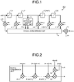
- FIG. 1 is a diagram illustrating an exemplary circuit configuration of a filter device according to the first embodiment of the present invention.
- the filter device 100 according to the first embodiment is a digital filter, specifically, an FIR filter.
- the filter device 100 is realized by, for example, a single circuit, a composite circuit, a programmed processor, a parallel programmed processor, an application specific integrated circuit (ASIC), a field programmable gate array (FPGA), or any combination thereof.
- ASIC application specific integrated circuit
- FPGA field programmable gate array
- the filter device 100 includes a plurality of delay units 1-1 to 1-N that delay an n-bit input signal by a predetermined time, multiplication units 2-0 to 2-N that multiply an input signal to the filter device 100 and delayed signals that are signals respectively outputted from the delay units 1-1 to 1-N by filter coefficients corresponding to these signals, a coefficient adjustment unit 3 that uses the m-th (m is one or more integers of [0 to N]) delayed signal, i.e.
- the multiplication signal of the signals outputted from the coefficient adjustment unit 3 means a signal that is obtained by multiplying the signals outputted from the coefficient adjustment unit 3 together.
- the delay units 1-1 to 1-N are connected in series, and the signal x(n) is inputted to the delay unit 1-1.
- the delayed signals outputted by the delay units 1-1 to 1-(N-1) are respectively input to the delay units 1-2 to 1-N in their subsequent stages, and are also inputted to the multiplication units 2-1 to 2-(N-1), respectively.
- the delayed signal outputted by the delay unit 1-N is inputted to the multiplication unit 2-N.
- the multiplication unit 2-0 receives the signal x(n).
- the multiplication units 2-0 to 2-N receive their corresponding filter coefficients in addition to the above signals.
- each filter coefficient by which the input signal x(n) or a delayed signal is multiplied is a value generated based on a pre-designed value (hereinafter referred to as a design value) h 0 , h 1 , ..., h N and a multiplying factor adjustment value A. More specifically, each filter coefficient is a value obtained by multiplying a predetermined design value by the multiplying factor adjustment value, or a value calculated based on a value obtained by multiplying a design value by the multiplying factor adjustment value. That is, the value of each filter coefficient is Ah 0 , Ah 1 , ..., Ah N or a value calculated based thereon.
- the filter coefficient when a first value obtained by multiplying a design value by the multiplying factor adjustment value is less than or equal to a maximum value C max of the representation range of the filter coefficient, the first value is used as the filter coefficient.
- a second value calculated based on the first value is used as the filter coefficient.
- Ah m %C max is the remainder of Ah m ⁇ C max . That is, when the first value Ah m exceeds the maximum value C max , the first value Ah m is divided by the maximum value C max to obtain a remainder that is the second value, and the obtained remainder is used as a filter coefficient. Note that when the first value Ah m is less than or equal to the maximum value C max , the remainder of Ah m ⁇ C max is equal to the first value Ah m . Therefore, it can be said that every filter coefficient is the remainder obtained by multiplying a design value by the multiplying factor adjustment value and dividing a resultant value of the multiplication by the maximum value C max of the representation range of the filter coefficient.
- the coefficient adjustment value [Ah m ] is an integer. That is, the coefficient adjustment value [Ah m ] is the quotient of Ah m ⁇ C max .
- FIG. 2 is a diagram illustrating an exemplary configuration of the signal conversion unit 4 provided in the filter device 100 according to the first embodiment.
- the signal conversion unit 4 includes addition units 41-1 to 41-(N+1) that use the outputs from the multiplication units 2-0 to 2-N as inputs thereof and add them while increasing the bit length.
- the signal conversion unit 4 includes a multiplication unit 42 that generates an adjusted signal by multiplying the m-th delayed signal x(n) and the coefficient adjustment value [Ah m ] outputted from the coefficient adjustment unit 3 with the bit length being increased, and an addition unit 43 that adds the output of the addition unit 41-(N+1) and the output of the multiplication unit 42.
- the number of multiplication units 42 and the number of addition units 43 are each not limited to one, and it is contemplated that that number may be greater than or equal to the number of filter coefficients exceeding the representation range through the multiplication of the multiplying factor adjustment value A. In this way, the signal conversion unit 4 obtains an output represented by the following expression (3).
- the coefficient adjustment unit 3 makes the same number of copies of the m-th delayed output as the coefficient adjustment value [Ah m ] and outputs the copies to the signal conversion unit 4, thereby to perform only addition without the need for multiplication in the signal conversion unit 4.
- the division unit 5 divides the output of the signal conversion unit 4 represented by the expression (3) by the multiplicand, namely the above-mentioned multiplying factor adjustment value A, and performs rounding such that the result has substantially the same bit length as x(n), thereby generating the output signal y(n) of the filter device 100 represented by the following equation (4).
- the division unit 5 can also be implemented by bit shift by setting the multiplying factor adjustment value A by which the filter coefficients are multiplied to a power of two.
- the output signal y(n) of the filter device 100 is represented by the following equation (5).
- em k denotes the computation error associated with multiplication.
- division can be performed using the equal multiplying factor adjustment value A with respect to the overall computation error, and thus the computation error can be reduced.
- the values of the filter coefficients multiplied by the multiplying factor adjustment value A are allowed to exceed the maximum value of the representation range, it is possible to improve the filter characteristics while keeping the quantization bit rate low.
- the filter device 100 includes two or more delay units 1-1 to 1-N that delay the input signal, the multiplication units 2-0 to 2-N that multiply the input signal x(n) and each of the delayed signals outputted from the delay units 1-1 to 1-N by the filter coefficients obtained by multiplying a design value by the multiplying factor adjustment value A, the coefficient adjustment unit 3 that generates a coefficient adjustment value based on the multiplying factor adjustment value A and the maximum value C max of the representation range when the filter coefficient exceeds the maximum value C max of the representation range, and outputs the generated coefficient adjustment value and the corresponding delayed signal, the signal conversion unit 4 that performs representation conversion by adding signals obtained by the filter coefficient multiplication outputted from the multiplication units 2-0 to 2-N and an adjusted signal obtained by multiplying the coefficient adjustment value outputted from the coefficient adjustment unit 3 and the delayed signal corresponding to this coefficient adjustment value, and the division unit 5 that divides the signal obtained by the representation conversion outputted from the signal conversion unit 4 by the multiplying factor adjustment value A.
- the filter device 100 the filter device 100,
- the filter device according to the second embodiment specifically, the filter device implemented using stochastic computing will be described.
- Stochastic computing is disclosed, for example, in the literature " Warren J. Gross and Vincent C. Gaudet Editors, 'Stochastic Computing: Techniques and Applications' ".
- Stochastic computing is characterized by its effectiveness in reducing the circuit scale of product-sum operation, and the filter device can be downsized by being configured using stochastic computing.
- stochastic computing a numerical value is expressed by the existence probability of zero and one in a bitstream generated using a random number sequence, so that the correlation in the random number sequence between numerical values inputted to the computing circuit becomes a cause of the computation error. Reducing this computation error is the problem to be considered when stochastic computing is used.
- FIG. 3 is a diagram illustrating an exemplary circuit configuration of a filter device 100a according to the second embodiment.
- the filter device 100a according to the second embodiment includes a representation conversion unit 6 (denoted by SNG (which stands for stochastic number generator) 6 in FIG.
- SNG stochastic number generator
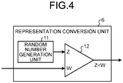
- FIG. 4 is a diagram illustrating an exemplary configuration of the representation conversion unit 6 provided in the filter device 100a according to the second embodiment.
- the representation conversion unit 6 includes a random number generation unit 11 that generates random numbers, and a comparator 12 that compares the input value to the representation conversion unit 6, namely the input signal x(n) to the filter device 100a, with the random number value inputted from the random number generation unit 11.
- the comparator 12 has a terminal Z to which the random number value is inputted, and a terminal W to which the signal x(n) is inputted.
- the comparator 12 outputs one when the binary-representation input value is larger than the random number value inputted from the random number generation unit 11, but outputs zero when the input value is less than or equal to the random number value.
- the bit length (hereinafter referred to as SN length) used for stochastic representation is 10 bits
- the input value is 0.3
- the random number value is uniform random numbers in a range between 0 and 1
- the resultant stochastic-representation value with the highest expected value corresponds to a number sequence in which 3 bits out of 10 bits have 1 and the remaining 7 bits have 0.
- the representation conversion unit 6 operates in this manner.
- the representation conversion unit 6 may be configured to generate stochastic-representation values corresponding to binary-representation values in advance, hold them in a memory as a table, and read the value corresponding to the input value directly from the memory.
- the after-conversion input signal in stochastic representation and the delayed signals in stochastic representation obtained by delaying the after-conversion input signal in stochastic representation in the delay units 1-1 to 1-N are multiplied by the corresponding filter coefficients in the multiplication units 7-0 to 7-N.
- the filter coefficients to be used in this process also need to be converted into stochastic representation.
- the filter coefficients Ah 0 , Ah 1 , ..., ⁇ Ah 0m ⁇ , ..., Ah N-1 , and Ah N illustrated in FIG. 3 are values already converted into stochastic representation in advance.
- a circuit equivalent to the representation conversion unit 6 may be provided separately as a coefficient conversion unit that converts the filter coefficients into stochastic representation.
- the multiplication units 7-0 to 7-N are expressed by AND operation, and this expression belongs to the case of unipolar representation with a stochastic representation range being set to 0 to 1. Instead, in the case of bipolar representation with a stochastic representation range being set to -1 to 1, the multiplication units 7-0 to 7-N are expressed by XNOR operation. These operations are realized by a lookup table (LUT) on an FPGA, for example.
- LUT lookup table
- the signal conversion unit 9 performs parallel addition using the outputs from the multiplication units 7-0 to 7-N and the outputs from the coefficient adjustment unit 8 as inputs.
- the parallel addition divides the number of "1" included in all the input stochastic-representation values by the SN length, thereby to obtain the output value represented in binary notation. For example, if the SN length is 10 and the input stochastic-representation values are three values, i.e., "0000100100" (0.2), “1010111110” (0.7), and "0010101111” (0.6), then 15 that is the number of "1s" is divided by the SN length of 10, and so 1.5 is obtained as the output value. By performing parallel addition through the above operation, the output represented in binary notation is obtained.
- the division unit 10 divides the output of the signal conversion unit 9 by the multiplicand, namely the above-mentioned multiplying factor adjustment value A, and performs rounding such that the result has the same bit length as x(n), thereby to generate the output signal y(n) of the filter device 100 represented by the following equation (6).
- the division unit 10 can also be realized by bit shift in which the multiplying factor adjustment value A by which filter coefficients are multiplied is set to a power of two, in substantially the same manner as the division unit 5 of the filter device 100 according to the first embodiment.
- the above configuration makes it possible to reduce a computation error because a computation error associated with parallel addition is only caused in the division of the number of "1s" by the SN length.
- a computation error associated with parallel addition is only caused in the division of the number of "1s" by the SN length.
- it is necessary to double the SN length in order to double the resolution in stochastic representation it is possible to reduce the circuit scale by reducing the SN length, and also to reduce the deterioration in filter characteristics due to computation error as in the first embodiment.
- the multiplication units 7-1 to 7-N can be implemented by simple circuitry, the overall circuit scale can be reduced.
- errors in stochastic representation are classified as conversion errors derived from conversion into stochastic representation and correlation errors derived from the correlation between random number sequences used for converting each input into stochastic representation during computation.
- the present embodiment describes a configuration for reducing a conversion error and a correlation error.
- the conversion error occurs when a random number sequence is biased.
- the representation conversion unit 6 of FIG. 4 expresses the range of 0 to 1 by stochastic representation with the SN length of 10.
- the random number generation unit 11 outputs uniform values, for example, 6 values that are each smaller than or equal to 0.6 and 4 values that are each larger than 0.6.
- the pseudo-random number generator has a biased output distribution caused, which increases the conversion error.
- a computation error is derived from the correlation between random number sequences used for converting each of inputs to the computation units into stochastic representation.
- the computation error associated with parallel addition is small. Therefore, a method for reducing a computation error in the multiplication units will be described below.
- An effective way to achieve this objective is, for example, to use ultra-uniform distribution sequences such as Sobol sequences as the random number sequences generated by the random number generation unit 11 of the representation conversion unit 6 and the random number sequences for converting filter coefficients into stochastic representation.
- Sobol sequences may be realized by sequentially reading out them from a conversion table, or may be realized in a method disclosed in the literature " 'Notes on generating Sobol sequences', Stephen Joe and Frances Y. Kuo, August 2008 ", for example.
- an ultra-uniform distribution sequence can be selected from among multiple sequences, it is effective to select two sequences that make the multiplication error smaller, and use one of the two for the representation conversion of a delayed signal and the other for the representation conversion of a filter coefficient.
- the above configuration makes it possible to reduce the conversion error associated with conversion into stochastic representation, and to further reduce the computation error associated with multiplication.
- 1-1 to 1-N delay unit 2-0 to 2-N, 7-0 to 7-N, 42 multiplication unit; 3, 8 coefficient adjustment unit; 4, 9 signal conversion unit; 5, 10 division unit; 6 representation conversion unit; 11 random number generation unit; 12 comparator; 41-1 to 41-(N+1), 43 addition unit; 100, 100a filter device.
Landscapes
- Engineering & Computer Science (AREA)
- Physics & Mathematics (AREA)
- Computer Hardware Design (AREA)
- Mathematical Physics (AREA)
- Theoretical Computer Science (AREA)
- Computing Systems (AREA)
- Complex Calculations (AREA)
- General Physics & Mathematics (AREA)
- Computational Mathematics (AREA)
- Mathematical Analysis (AREA)
- Mathematical Optimization (AREA)
- Pure & Applied Mathematics (AREA)
- General Engineering & Computer Science (AREA)
Abstract
Description
- The present invention relates to a filter device that filters a digital signal.
- A finite impulse response filter (hereinafter referred to as an FIR filter) is a kind of a digital filter, which convolves an input signal with filter coefficients and outputs a resultant signal obtained by the convolution.
- In digital filters, quantization noise and computation error have been known to be a cause for deterioration in filter characteristics.
- The quantization noise has a problem that the noise increases as the length of a filter increases. Regarding this problem,
Patent Literature 1 describes an inventive technique for reducing the quantization noise of filter coefficients. In the inventive technique described inPatent Literature 1, each filter coefficient of the digital filter is multiplied by an adjustment multiplying factor value to make adjustment, and input data is multiplied by the filter coefficients obtained after the adjustment. Next, the input data having been multiplied by the adjusted filter coefficients is divided by the multiplicand, thereby to reduce the error caused by the rounding of the filter coefficients of the long digital filter. - Patent Literature 1:
Japanese Patent Application Laid-open No. H3-46813 - In some cases, however, the inventive technique described in
Patent Literature 1 cannot sufficiently reduce the computation error. Below is a detailed description of this issue. - Consider the conventional FIR filter illustrated in No. 4 of
Patent Literature 1. For convenience of explanation, the input signal to the FIR filter is denoted by x(n), the output signal is denoted by y(n), and each filter coefficient is denoted by hn (n=0, 1, ..., N-1).
The input signal x(n) and each filter coefficient hn contain their respective quantization noises. Let emk represent the computation error caused through multiplication of the input signal x(n) and the k-th filter coefficient hk, and eak represent the error caused through addition thereof, then the output signal y(n) is expressed by the following equation (1). - [Formula 1]

- In order to correct the error caused by the rounding of filter coefficients as in the inventive technique described in
Patent Literature 1, when the k-th filter coefficient hk is subjected to preliminary multiplying factor adjustment with ck and then divided by ck, the output signal y(n) is expressed by the following equation (2). - [Formula 2]

- When the filter coefficient hk has a relatively large value among all the filter coefficients (ho, hi, ..., hN-1), if the range in which the filter coefficient is represented is small, then the value ck for the preliminary multiplying factor adjustment cannot have a large value, and the second term representing the computation error caused by multiplication in the equation (2) does not have a small value. That is, the computation error cannot be satisfactorily reduced.
- The present invention has been made in view of the above circumstances, and an object thereof is to provide a filter device capable of reducing the deterioration in filter characteristics due to a computation error.
- In order to solve the above-mentioned problems and achieve the object, the present invention provides a filter device comprising: a plurality of delay units connected in series to delay an input signal in response to reception of the input signal and to output a delayed signal; a plurality of multiplication units to multiply the delayed signal by a filter coefficient generated based on a predetermined value and a multiplying factor adjustment value; a coefficient adjustment unit to, when a multiplication result obtained by multiplying the predetermined value by the multiplying factor adjustment value exceeds a maximum value of a representation range of the filter coefficient, divide the multiplication result exceeding the maximum value by the maximum value, and output a quotient of the division as a coefficient adjustment value; a signal conversion unit to output a signal obtained by adding after-filter-coefficient-multiplication signals outputted by the plurality of multiplication units and an adjusted signal obtained by adjusting a corresponding delayed signal using the coefficient adjustment value; and a division unit to generate an output signal by dividing the signal outputted by the signal conversion unit by the multiplying factor adjustment value.
- The filter device according to the present invention has an advantageous effect that it can reduce the deterioration in filter characteristics due to a computation error.
-
-
FIG. 1 is a diagram illustrating an exemplary circuit configuration of a filter device according to a first embodiment of the present invention. -
FIG. 2 is a diagram illustrating an exemplary configuration of a signal conversion unit provided in the filter device according to the first embodiment. -
FIG. 3 is a diagram illustrating an exemplary circuit configuration of a filter device according to a second embodiment of the present invention. -
FIG. 4 is a diagram illustrating an exemplary configuration of a representation conversion unit provided in the filter device according to the second embodiment. - Hereinafter, a filter device according to embodiments of the present invention will be described in detail with reference to the drawings. It is noted that the present invention is not necessarily limited by these embodiments.
-
FIG. 1 is a diagram illustrating an exemplary circuit configuration of a filter device according to the first embodiment of the present invention. Thefilter device 100 according to the first embodiment is a digital filter, specifically, an FIR filter. In a case where thefilter device 100 is implemented by dedicated hardware, thefilter device 100 is realized by, for example, a single circuit, a composite circuit, a programmed processor, a parallel programmed processor, an application specific integrated circuit (ASIC), a field programmable gate array (FPGA), or any combination thereof. - As illustrated in
FIG. 1 , thefilter device 100 includes a plurality of delay units 1-1 to 1-N that delay an n-bit input signal by a predetermined time, multiplication units 2-0 to 2-N that multiply an input signal to thefilter device 100 and delayed signals that are signals respectively outputted from the delay units 1-1 to 1-N by filter coefficients corresponding to these signals, acoefficient adjustment unit 3 that uses the m-th (m is one or more integers of [0 to N]) delayed signal, i.e. the delayed signal outputted from the delay unit 1-m as an input and makes outputs for a signal conversion unit 4 (described later), thesignal conversion unit 4 that performs representation conversion by adding the signals from the multiplication units 2-0 to 2-N and the multiplication signal of the signals outputted from thecoefficient adjustment unit 3, and a division unit 5 that divides the output signal from thesignal conversion unit 4 by the multiplicand. The multiplication signal of the signals outputted from thecoefficient adjustment unit 3 means a signal that is obtained by multiplying the signals outputted from thecoefficient adjustment unit 3 together. - The delay units 1-1 to 1-N are connected in series, and the signal x(n) is inputted to the delay unit 1-1. The delayed signals outputted by the delay units 1-1 to 1-(N-1) are respectively input to the delay units 1-2 to 1-N in their subsequent stages, and are also inputted to the multiplication units 2-1 to 2-(N-1), respectively. The delayed signal outputted by the delay unit 1-N is inputted to the multiplication unit 2-N. The multiplication unit 2-0 receives the signal x(n). The multiplication units 2-0 to 2-N receive their corresponding filter coefficients in addition to the above signals.
- Here, each filter coefficient by which the input signal x(n) or a delayed signal is multiplied is a value generated based on a pre-designed value (hereinafter referred to as a design value) h0, h1, ..., hN and a multiplying factor adjustment value A. More specifically, each filter coefficient is a value obtained by multiplying a predetermined design value by the multiplying factor adjustment value, or a value calculated based on a value obtained by multiplying a design value by the multiplying factor adjustment value. That is, the value of each filter coefficient is Ah0, Ah1, ..., AhN or a value calculated based thereon. In the present embodiment, when a first value obtained by multiplying a design value by the multiplying factor adjustment value is less than or equal to a maximum value Cmax of the representation range of the filter coefficient, the first value is used as the filter coefficient. When the first value exceeds the maximum value Cmax, a second value calculated based on the first value is used as the filter coefficient. Specifically, when the value of the m-th coefficient exceeds the maximum value Cmax of the representation range of the filter coefficient through the multiplication of the design value by the multiplying factor adjustment value A, {Ahm}=Ahm%Cmax is inputted to the multiplication unit 2-m as a filter coefficient by which the m-th delayed signal is multiplied. Here, Ahm%Cmax is the remainder of Ahm÷Cmax. That is, when the first value Ahm exceeds the maximum value Cmax, the first value Ahm is divided by the maximum value Cmax to obtain a remainder that is the second value, and the obtained remainder is used as a filter coefficient. Note that when the first value Ahm is less than or equal to the maximum value Cmax, the remainder of Ahm÷Cmax is equal to the first value Ahm. Therefore, it can be said that every filter coefficient is the remainder obtained by multiplying a design value by the multiplying factor adjustment value and dividing a resultant value of the multiplication by the maximum value Cmax of the representation range of the filter coefficient.
- The
coefficient adjustment unit 3 outputs, to thesignal conversion unit 4, the m-th delayed signal inputted from the delay unit 1-m and the coefficient adjustment value [Ahm]=Ahm/Cmax. Note that the coefficient adjustment value [Ahm] is an integer. That is, the coefficient adjustment value [Ahm] is the quotient of Ahm÷Cmax. - The
signal conversion unit 4 will be described.FIG. 2 is a diagram illustrating an exemplary configuration of thesignal conversion unit 4 provided in thefilter device 100 according to the first embodiment. - The
signal conversion unit 4 includes addition units 41-1 to 41-(N+1) that use the outputs from the multiplication units 2-0 to 2-N as inputs thereof and add them while increasing the bit length. The addition unit 41-k (k=2, 3, 4, ..., N+1) adds the signal outputted by the addition unit 41-(k-1) and the signal outputted by the multiplication unit 2-k. In addition, thesignal conversion unit 4 includes amultiplication unit 42 that generates an adjusted signal by multiplying the m-th delayed signal x(n) and the coefficient adjustment value [Ahm] outputted from thecoefficient adjustment unit 3 with the bit length being increased, and anaddition unit 43 that adds the output of the addition unit 41-(N+1) and the output of themultiplication unit 42. The number ofmultiplication units 42 and the number ofaddition units 43 are each not limited to one, and it is contemplated that that number may be greater than or equal to the number of filter coefficients exceeding the representation range through the multiplication of the multiplying factor adjustment value A. In this way, thesignal conversion unit 4 obtains an output represented by the following expression (3). - [Formula 3]

- Alternatively, another configuration may be used in which the
coefficient adjustment unit 3 makes the same number of copies of the m-th delayed output as the coefficient adjustment value [Ahm] and outputs the copies to thesignal conversion unit 4, thereby to perform only addition without the need for multiplication in thesignal conversion unit 4. - The division unit 5 divides the output of the
signal conversion unit 4 represented by the expression (3) by the multiplicand, namely the above-mentioned multiplying factor adjustment value A, and performs rounding such that the result has substantially the same bit length as x(n), thereby generating the output signal y(n) of thefilter device 100 represented by the following equation (4). - [Formula 4]

- The division unit 5 can also be implemented by bit shift by setting the multiplying factor adjustment value A by which the filter coefficients are multiplied to a power of two.
- By the above configuration, it is expected that the computation error associated with addition in the
filter device 100 is minimized. At this time, only in terms of the computation error associated with multiplication, the output signal y(n) of thefilter device 100 is represented by the following equation (5). In the equation (5), emk denotes the computation error associated with multiplication. - [Formula 5]

- As shown by the second term of the equation (5), division can be performed using the equal multiplying factor adjustment value A with respect to the overall computation error, and thus the computation error can be reduced. In addition, because the values of the filter coefficients multiplied by the multiplying factor adjustment value A are allowed to exceed the maximum value of the representation range, it is possible to improve the filter characteristics while keeping the quantization bit rate low.
- As described above, the filter device 100 according to the first embodiment includes two or more delay units 1-1 to 1-N that delay the input signal, the multiplication units 2-0 to 2-N that multiply the input signal x(n) and each of the delayed signals outputted from the delay units 1-1 to 1-N by the filter coefficients obtained by multiplying a design value by the multiplying factor adjustment value A, the coefficient adjustment unit 3 that generates a coefficient adjustment value based on the multiplying factor adjustment value A and the maximum value Cmax of the representation range when the filter coefficient exceeds the maximum value Cmax of the representation range, and outputs the generated coefficient adjustment value and the corresponding delayed signal, the signal conversion unit 4 that performs representation conversion by adding signals obtained by the filter coefficient multiplication outputted from the multiplication units 2-0 to 2-N and an adjusted signal obtained by multiplying the coefficient adjustment value outputted from the coefficient adjustment unit 3 and the delayed signal corresponding to this coefficient adjustment value, and the division unit 5 that divides the signal obtained by the representation conversion outputted from the signal conversion unit 4 by the multiplying factor adjustment value A. According to the filter device 100, it is possible to reduce the deterioration in filter characteristics possibly caused by the computation error.
- Next, the filter device according to the second embodiment, specifically, the filter device implemented using stochastic computing will be described.
- Stochastic computing is disclosed, for example, in the literature "Warren J. Gross and Vincent C. Gaudet Editors, 'Stochastic Computing: Techniques and Applications'".
- Stochastic computing is characterized by its effectiveness in reducing the circuit scale of product-sum operation, and the filter device can be downsized by being configured using stochastic computing. In other hand, in stochastic computing, a numerical value is expressed by the existence probability of zero and one in a bitstream generated using a random number sequence, so that the correlation in the random number sequence between numerical values inputted to the computing circuit becomes a cause of the computation error. Reducing this computation error is the problem to be considered when stochastic computing is used.
-
FIG. 3 is a diagram illustrating an exemplary circuit configuration of afilter device 100a according to the second embodiment. Thefilter device 100a according to the second embodiment includes a representation conversion unit 6 (denoted by SNG (which stands for stochastic number generator) 6 inFIG. 3 ) that converts the n-bit input signal x(n) in binary notation into stochastic representation, two or more delay units 1-1 to 1-N that delay the input signal from therepresentation conversion unit 6 by their predetermined times, multiplication units 7-0 to 7-N that multiply the input signal from therepresentation conversion unit 6 and the delayed signals outputted from the delay units 1-1 to 1-N by the filter coefficients corresponding to these signals, a coefficient adjustment unit 8 that uses the m-th delayed signal as its input and makes output to a signal conversion unit 9 (described later), the signal conversion unit 9 that performs representation conversion by adding the signals from the multiplication units 7-0 to 7-N and the multiplication signal of the signals outputted from the coefficient adjustment unit 8, and adivision unit 10 that divides the output signal from the signal conversion unit 9 by the multiplicand. The stochastic-representation signal outputted by therepresentation conversion unit 6 is inputted to the leading delay unit 1-1 of the delay units 1-1 to 1-N. - The
representation conversion unit 6 will be described.FIG. 4 is a diagram illustrating an exemplary configuration of therepresentation conversion unit 6 provided in thefilter device 100a according to the second embodiment. - The
representation conversion unit 6 includes a randomnumber generation unit 11 that generates random numbers, and a comparator 12 that compares the input value to therepresentation conversion unit 6, namely the input signal x(n) to thefilter device 100a, with the random number value inputted from the randomnumber generation unit 11. The comparator 12 has a terminal Z to which the random number value is inputted, and a terminal W to which the signal x(n) is inputted. - The comparator 12 outputs one when the binary-representation input value is larger than the random number value inputted from the random
number generation unit 11, but outputs zero when the input value is less than or equal to the random number value. With such a configuration, for example, if the bit length (hereinafter referred to as SN length) used for stochastic representation is 10 bits, the input value is 0.3, and the random number value is uniform random numbers in a range between 0 and 1, then the resultant stochastic-representation value with the highest expected value corresponds to a number sequence in which 3 bits out of 10 bits have 1 and the remaining 7 bits have 0. Therepresentation conversion unit 6 operates in this manner. Therepresentation conversion unit 6 may be configured to generate stochastic-representation values corresponding to binary-representation values in advance, hold them in a memory as a table, and read the value corresponding to the input value directly from the memory. - The after-conversion input signal in stochastic representation and the delayed signals in stochastic representation obtained by delaying the after-conversion input signal in stochastic representation in the delay units 1-1 to 1-N are multiplied by the corresponding filter coefficients in the multiplication units 7-0 to 7-N. The filter coefficients to be used in this process also need to be converted into stochastic representation. The filter coefficients Ah0, Ah1, ..., {Ah0m}, ..., AhN-1, and AhN illustrated in
FIG. 3 are values already converted into stochastic representation in advance. Alternatively, a circuit equivalent to therepresentation conversion unit 6 may be provided separately as a coefficient conversion unit that converts the filter coefficients into stochastic representation. - In
FIG. 3 , the multiplication units 7-0 to 7-N are expressed by AND operation, and this expression belongs to the case of unipolar representation with a stochastic representation range being set to 0 to 1. Instead, in the case of bipolar representation with a stochastic representation range being set to -1 to 1, the multiplication units 7-0 to 7-N are expressed by XNOR operation. These operations are realized by a lookup table (LUT) on an FPGA, for example. - The coefficient adjustment unit 8 outputs, to the signal conversion unit 9, the m-th delayed signal inputted from the delay unit 1-m and the coefficient adjustment value [Ahm]=Ahm/Cmax, in substantially the same manner as the
coefficient adjustment unit 3 of thefilter device 100 according to the first embodiment. - The signal conversion unit 9 performs parallel addition using the outputs from the multiplication units 7-0 to 7-N and the outputs from the coefficient adjustment unit 8 as inputs. In this example, the parallel addition divides the number of "1" included in all the input stochastic-representation values by the SN length, thereby to obtain the output value represented in binary notation. For example, if the SN length is 10 and the input stochastic-representation values are three values, i.e., "0000100100" (0.2), "1010111110" (0.7), and "0010101111" (0.6), then 15 that is the number of "1s" is divided by the SN length of 10, and so 1.5 is obtained as the output value. By performing parallel addition through the above operation, the output represented in binary notation is obtained.
- The
division unit 10 divides the output of the signal conversion unit 9 by the multiplicand, namely the above-mentioned multiplying factor adjustment value A, and performs rounding such that the result has the same bit length as x(n), thereby to generate the output signal y(n) of thefilter device 100 represented by the following equation (6). - [Formula 6]

- The
division unit 10 can also be realized by bit shift in which the multiplying factor adjustment value A by which filter coefficients are multiplied is set to a power of two, in substantially the same manner as the division unit 5 of thefilter device 100 according to the first embodiment. - The above configuration makes it possible to reduce a computation error because a computation error associated with parallel addition is only caused in the division of the number of "1s" by the SN length. In particular, because it is necessary to double the SN length in order to double the resolution in stochastic representation, it is possible to reduce the circuit scale by reducing the SN length, and also to reduce the deterioration in filter characteristics due to computation error as in the first embodiment. Further, because the multiplication units 7-1 to 7-N can be implemented by simple circuitry, the overall circuit scale can be reduced.
- In the filter device of a configuration according to the second embodiment, errors in stochastic representation are classified as conversion errors derived from conversion into stochastic representation and correlation errors derived from the correlation between random number sequences used for converting each input into stochastic representation during computation. The present embodiment describes a configuration for reducing a conversion error and a correlation error.
- The conversion error occurs when a random number sequence is biased. For example, suppose that the
representation conversion unit 6 ofFIG. 4 expresses the range of 0 to 1 by stochastic representation with the SN length of 10. In this case, in order to convert the value 0.6 into stochastic representation, it is desirable that the randomnumber generation unit 11 outputs uniform values, for example, 6 values that are each smaller than or equal to 0.6 and 4 values that are each larger than 0.6. However, the pseudo-random number generator has a biased output distribution caused, which increases the conversion error. - In addition, a computation error is derived from the correlation between random number sequences used for converting each of inputs to the computation units into stochastic representation. In the configuration described in the second embodiment, the computation error associated with parallel addition is small. Therefore, a method for reducing a computation error in the multiplication units will be described below.
- In the
filter device 100a with the configuration of the second embodiment, as the correlation between random number sequences for converting, into stochastic representation, delayed signals and filter coefficients which are inputs to the multiplication units 7-0 to 7-N gets larger, the error is larger. Therefore, in order to reduce the computation error, random number sequences used for converting each delayed signal and each filter coefficient into stochastic representation need to have a small correlation. - An effective way to achieve this objective is, for example, to use ultra-uniform distribution sequences such as Sobol sequences as the random number sequences generated by the random
number generation unit 11 of therepresentation conversion unit 6 and the random number sequences for converting filter coefficients into stochastic representation. Sobol sequences may be realized by sequentially reading out them from a conversion table, or may be realized in a method disclosed in the literature "'Notes on generating Sobol sequences', Stephen Joe and Frances Y. Kuo, August 2008", for example. - In addition, in a case where an ultra-uniform distribution sequence can be selected from among multiple sequences, it is effective to select two sequences that make the multiplication error smaller, and use one of the two for the representation conversion of a delayed signal and the other for the representation conversion of a filter coefficient.
- The above configuration makes it possible to reduce the conversion error associated with conversion into stochastic representation, and to further reduce the computation error associated with multiplication.
- The configurations described in the above-mentioned embodiments show examples of the contents of the present invention, and can each be combined with other publicly known techniques and partially omitted and/or modified without departing from the scope of the present invention.
- 1-1 to 1-N delay unit; 2-0 to 2-N, 7-0 to 7-N, 42 multiplication unit; 3, 8 coefficient adjustment unit; 4, 9 signal conversion unit; 5, 10 division unit; 6 representation conversion unit; 11 random number generation unit; 12 comparator; 41-1 to 41-(N+1), 43 addition unit; 100, 100a filter device.
Claims (9)
- A filter device comprising:a plurality of delay units connected in series to delay an input signal in response to reception of the input signal and to output a delayed signal;a plurality of multiplication units to multiply the delayed signal by a filter coefficient generated based on a predetermined value and a multiplying factor adjustment value;a coefficient adjustment unit to, when a multiplication result obtained by multiplying the predetermined value by the multiplying factor adjustment value exceeds a maximum value of a representation range of the filter coefficient, divide the multiplication result exceeding the maximum value by the maximum value, and output a quotient of the division as a coefficient adjustment value;a signal conversion unit to output a signal obtained by adding after-filter-coefficient-multiplication signals outputted by the plurality of multiplication units and an adjusted signal obtained by adjusting a corresponding delayed signal using the coefficient adjustment value; anda division unit to generate an output signal by dividing the signal outputted by the signal conversion unit by the multiplying factor adjustment value.
- The filter device according to claim 1, wherein
a remainder obtained by dividing the multiplication result by the maximum value is used as the filter coefficient. - The filter device according to claim 1 or 2, wherein
the signal conversion unit obtains the adjusted signal by multiplying the corresponding delayed signal by the coefficient adjustment value. - The filter device according to claim 1 or 2, whereinthe coefficient adjustment unit outputs the same number of the delayed signals corresponding to the coefficient adjustment value as the number of the coefficient adjustment values, andthe signal conversion unit obtains the adjusted signal by adding the delayed signals corresponding to the coefficient adjustment value outputted by the coefficient adjustment unit.
- The filter device according to any one of claims 1 to 4, whereinthe multiplying factor adjustment value is set to a power of two, anddivision processing performed by the division unit is implemented by bit shift.
- The filter device according to any one of claims 1 to 5, comprisinga representation conversion unit to convert an input signal into a stochastic-representation signal and input the stochastic-representation signal to a leading delay unit of the plurality of delay units, whereinthe filter coefficient is a stochastic-representation filter coefficient, andthe coefficient adjustment unit and the signal conversion unit perform computation processing on the stochastic-representation signal.
- The filter device according to claim 6, comprising
a coefficient conversion unit to convert the filter coefficient into the stochastic-representation filter coefficient. - The filter device according to claim 6 or 7, wherein
the representation conversion unit converts an input signal into a stochastic-representation signal using an ultra-uniform distribution sequence. - The filter device according to any one of claims 6 to 8, comprising
a coefficient conversion unit to convert the filter coefficient into the stochastic-representation filter coefficient using an ultra-uniform distribution sequence.
Applications Claiming Priority (1)
| Application Number | Priority Date | Filing Date | Title |
|---|---|---|---|
| PCT/JP2019/049224 WO2021124413A1 (en) | 2019-12-16 | 2019-12-16 | Filter device |
Publications (3)
| Publication Number | Publication Date |
|---|---|
| EP4044433A1 true EP4044433A1 (en) | 2022-08-17 |
| EP4044433A4 EP4044433A4 (en) | 2022-10-26 |
| EP4044433B1 EP4044433B1 (en) | 2024-06-26 |
Family
ID=76477301
Family Applications (1)
| Application Number | Title | Priority Date | Filing Date |
|---|---|---|---|
| EP19956841.1A Active EP4044433B1 (en) | 2019-12-16 | 2019-12-16 | Finite impulse response filter (fir) |
Country Status (5)
| Country | Link |
|---|---|
| US (1) | US11894822B2 (en) |
| EP (1) | EP4044433B1 (en) |
| JP (1) | JP7076655B2 (en) |
| CA (1) | CA3158143A1 (en) |
| WO (1) | WO2021124413A1 (en) |
Families Citing this family (1)
| Publication number | Priority date | Publication date | Assignee | Title |
|---|---|---|---|---|
| CN120691943B (en) * | 2025-08-13 | 2026-02-10 | 中国电子科技集团公司第五十四研究所 | A dual-link angle error fusion device for a microwave laser composite system |
Family Cites Families (7)
| Publication number | Priority date | Publication date | Assignee | Title |
|---|---|---|---|---|
| JPH0720047B2 (en) * | 1985-11-01 | 1995-03-06 | ソニー株式会社 | Digital Filter |
| US5128886A (en) * | 1989-07-14 | 1992-07-07 | Tektronix, Inc. | Using long distance filters in the presence of round-off errors |
| JP2930325B2 (en) * | 1989-07-29 | 1999-08-03 | ソニー株式会社 | Digital signal processing circuit |
| JPH09199926A (en) * | 1996-01-17 | 1997-07-31 | Atr Hikari Denpa Tsushin Kenkiyushiyo:Kk | Adaptive digital beamforming device |
| US6505221B1 (en) * | 1999-09-20 | 2003-01-07 | Koninklijke Philips Electronics N.V. | FIR filter utilizing programmable shifter |
| JP2006093884A (en) * | 2004-09-21 | 2006-04-06 | Oki Electric Ind Co Ltd | Filtering device |
| JP2009129302A (en) | 2007-11-27 | 2009-06-11 | Panasonic Corp | Learning method of neural network elements by probabilistic arithmetic |
-
2019
- 2019-12-16 CA CA3158143A patent/CA3158143A1/en not_active Abandoned
- 2019-12-16 JP JP2021558571A patent/JP7076655B2/en active Active
- 2019-12-16 EP EP19956841.1A patent/EP4044433B1/en active Active
- 2019-12-16 WO PCT/JP2019/049224 patent/WO2021124413A1/en not_active Ceased
-
2022
- 2022-04-11 US US17/717,483 patent/US11894822B2/en active Active
Also Published As
| Publication number | Publication date |
|---|---|
| JP7076655B2 (en) | 2022-05-27 |
| EP4044433B1 (en) | 2024-06-26 |
| US11894822B2 (en) | 2024-02-06 |
| US20220239283A1 (en) | 2022-07-28 |
| WO2021124413A1 (en) | 2021-06-24 |
| CA3158143A1 (en) | 2021-06-24 |
| JPWO2021124413A1 (en) | 2021-06-24 |
| EP4044433A4 (en) | 2022-10-26 |
Similar Documents
| Publication | Publication Date | Title |
|---|---|---|
| KR100253987B1 (en) | Method and apparatus for performing fast Hadamard transformation | |
| IL278043B2 (en) | A method for simplifying a filter and related devices | |
| US12061664B2 (en) | Method for filtering with reduced latency and associated devices | |
| US20220239283A1 (en) | Filter device | |
| US11436302B2 (en) | Electronic system for computing items of an outer product matrix | |
| US10721104B2 (en) | Feed forward equalizer with power-optimized distributed arithmetic architecture and method | |
| US6745219B1 (en) | Arithmetic unit using stochastic data processing | |
| WO2023134507A1 (en) | Stochastic calculation method, circuit, chip, and device | |
| US7830949B2 (en) | Cross correlation circuits and methods | |
| US20200104131A1 (en) | Method for Operating a Digital Computer to Reduce the Computational Complexity Associated with Dot Products between Large Vectors | |
| Cardarilli et al. | Programmable power-of-two RNS scaler and its application to a QRNS polyphase filter | |
| US12019700B2 (en) | Signal processing apparatus, method, program, and recording medium | |
| CN109379191B (en) | Dot multiplication operation circuit and method based on elliptic curve base point | |
| Wu et al. | Improving common subexpression elimination algorithm with a new gate-level delay computing method | |
| EP3379407A1 (en) | Embedded system, communication unit and method for implementing an exponential computation | |
| SE444730B (en) | LJUDSYNTETISATOR | |
| Matutino et al. | Binary-to-RNS Conversion Units for moduli {2^ n±3} | |
| Pushpa et al. | Area optimized implementation of Galois field Fourier transform | |
| KR101318992B1 (en) | Modulo n calculation method and apparatus thereof | |
| US8370413B1 (en) | No-multiply finite impulse response (FIR) filter using phase additions | |
| JP4738408B2 (en) | Matrix operation unit | |
| Meteer et al. | An optimal variable-latency architecture for deterministic approaches to stochastic computing with unary bit stream preserving properties | |
| JP2000132539A (en) | Arithmetic unit | |
| Vinisha¹ et al. | Efficient Fir Filter Design Using Distributed Arithmetic Logic | |
| KR20020054202A (en) | Apaaratus for calculating inversion of multi level structure in the finite field |
Legal Events
| Date | Code | Title | Description |
|---|---|---|---|
| STAA | Information on the status of an ep patent application or granted ep patent |
Free format text: STATUS: THE INTERNATIONAL PUBLICATION HAS BEEN MADE |
|
| PUAI | Public reference made under article 153(3) epc to a published international application that has entered the european phase |
Free format text: ORIGINAL CODE: 0009012 |
|
| STAA | Information on the status of an ep patent application or granted ep patent |
Free format text: STATUS: REQUEST FOR EXAMINATION WAS MADE |
|
| 17P | Request for examination filed |
Effective date: 20220415 |
|
| AK | Designated contracting states |
Kind code of ref document: A1 Designated state(s): AL AT BE BG CH CY CZ DE DK EE ES FI FR GB GR HR HU IE IS IT LI LT LU LV MC MK MT NL NO PL PT RO RS SE SI SK SM TR |
|
| A4 | Supplementary search report drawn up and despatched |
Effective date: 20220923 |
|
| RIC1 | Information provided on ipc code assigned before grant |
Ipc: H03H 17/02 20060101ALI20220919BHEP Ipc: H03H 17/06 20060101AFI20220919BHEP |
|
| DAV | Request for validation of the european patent (deleted) | ||
| DAX | Request for extension of the european patent (deleted) | ||
| STAA | Information on the status of an ep patent application or granted ep patent |
Free format text: STATUS: EXAMINATION IS IN PROGRESS |
|
| 17Q | First examination report despatched |
Effective date: 20230714 |
|
| GRAP | Despatch of communication of intention to grant a patent |
Free format text: ORIGINAL CODE: EPIDOSNIGR1 |
|
| STAA | Information on the status of an ep patent application or granted ep patent |
Free format text: STATUS: GRANT OF PATENT IS INTENDED |
|
| INTG | Intention to grant announced |
Effective date: 20240208 |
|
| GRAS | Grant fee paid |
Free format text: ORIGINAL CODE: EPIDOSNIGR3 |
|
| GRAA | (expected) grant |
Free format text: ORIGINAL CODE: 0009210 |
|
| STAA | Information on the status of an ep patent application or granted ep patent |
Free format text: STATUS: THE PATENT HAS BEEN GRANTED |
|
| AK | Designated contracting states |
Kind code of ref document: B1 Designated state(s): AL AT BE BG CH CY CZ DE DK EE ES FI FR GB GR HR HU IE IS IT LI LT LU LV MC MK MT NL NO PL PT RO RS SE SI SK SM TR |
|
| REG | Reference to a national code |
Ref country code: GB Ref legal event code: FG4D |
|
| REG | Reference to a national code |
Ref country code: CH Ref legal event code: EP |
|
| REG | Reference to a national code |
Ref country code: DE Ref legal event code: R096 Ref document number: 602019054427 Country of ref document: DE |
|
| PG25 | Lapsed in a contracting state [announced via postgrant information from national office to epo] |
Ref country code: BG Free format text: LAPSE BECAUSE OF FAILURE TO SUBMIT A TRANSLATION OF THE DESCRIPTION OR TO PAY THE FEE WITHIN THE PRESCRIBED TIME-LIMIT Effective date: 20240626 |
|
| PG25 | Lapsed in a contracting state [announced via postgrant information from national office to epo] |
Ref country code: FI Free format text: LAPSE BECAUSE OF FAILURE TO SUBMIT A TRANSLATION OF THE DESCRIPTION OR TO PAY THE FEE WITHIN THE PRESCRIBED TIME-LIMIT Effective date: 20240626 Ref country code: HR Free format text: LAPSE BECAUSE OF FAILURE TO SUBMIT A TRANSLATION OF THE DESCRIPTION OR TO PAY THE FEE WITHIN THE PRESCRIBED TIME-LIMIT Effective date: 20240626 |
|
| REG | Reference to a national code |
Ref country code: LT Ref legal event code: MG9D |
|
| PG25 | Lapsed in a contracting state [announced via postgrant information from national office to epo] |
Ref country code: GR Free format text: LAPSE BECAUSE OF FAILURE TO SUBMIT A TRANSLATION OF THE DESCRIPTION OR TO PAY THE FEE WITHIN THE PRESCRIBED TIME-LIMIT Effective date: 20240927 |
|
| PG25 | Lapsed in a contracting state [announced via postgrant information from national office to epo] |
Ref country code: LV Free format text: LAPSE BECAUSE OF FAILURE TO SUBMIT A TRANSLATION OF THE DESCRIPTION OR TO PAY THE FEE WITHIN THE PRESCRIBED TIME-LIMIT Effective date: 20240626 |
|
| REG | Reference to a national code |
Ref country code: NL Ref legal event code: MP Effective date: 20240626 |
|
| PG25 | Lapsed in a contracting state [announced via postgrant information from national office to epo] |
Ref country code: NO Free format text: LAPSE BECAUSE OF FAILURE TO SUBMIT A TRANSLATION OF THE DESCRIPTION OR TO PAY THE FEE WITHIN THE PRESCRIBED TIME-LIMIT Effective date: 20240926 Ref country code: LV Free format text: LAPSE BECAUSE OF FAILURE TO SUBMIT A TRANSLATION OF THE DESCRIPTION OR TO PAY THE FEE WITHIN THE PRESCRIBED TIME-LIMIT Effective date: 20240626 Ref country code: HR Free format text: LAPSE BECAUSE OF FAILURE TO SUBMIT A TRANSLATION OF THE DESCRIPTION OR TO PAY THE FEE WITHIN THE PRESCRIBED TIME-LIMIT Effective date: 20240626 Ref country code: GR Free format text: LAPSE BECAUSE OF FAILURE TO SUBMIT A TRANSLATION OF THE DESCRIPTION OR TO PAY THE FEE WITHIN THE PRESCRIBED TIME-LIMIT Effective date: 20240927 Ref country code: FI Free format text: LAPSE BECAUSE OF FAILURE TO SUBMIT A TRANSLATION OF THE DESCRIPTION OR TO PAY THE FEE WITHIN THE PRESCRIBED TIME-LIMIT Effective date: 20240626 Ref country code: BG Free format text: LAPSE BECAUSE OF FAILURE TO SUBMIT A TRANSLATION OF THE DESCRIPTION OR TO PAY THE FEE WITHIN THE PRESCRIBED TIME-LIMIT Effective date: 20240626 Ref country code: RS Free format text: LAPSE BECAUSE OF FAILURE TO SUBMIT A TRANSLATION OF THE DESCRIPTION OR TO PAY THE FEE WITHIN THE PRESCRIBED TIME-LIMIT Effective date: 20240926 |
|
| PG25 | Lapsed in a contracting state [announced via postgrant information from national office to epo] |
Ref country code: NL Free format text: LAPSE BECAUSE OF FAILURE TO SUBMIT A TRANSLATION OF THE DESCRIPTION OR TO PAY THE FEE WITHIN THE PRESCRIBED TIME-LIMIT Effective date: 20240626 |
|
| REG | Reference to a national code |
Ref country code: AT Ref legal event code: MK05 Ref document number: 1698546 Country of ref document: AT Kind code of ref document: T Effective date: 20240626 |
|
| PG25 | Lapsed in a contracting state [announced via postgrant information from national office to epo] |
Ref country code: NL Free format text: LAPSE BECAUSE OF FAILURE TO SUBMIT A TRANSLATION OF THE DESCRIPTION OR TO PAY THE FEE WITHIN THE PRESCRIBED TIME-LIMIT Effective date: 20240626 |
|
| PG25 | Lapsed in a contracting state [announced via postgrant information from national office to epo] |
Ref country code: PT Free format text: LAPSE BECAUSE OF FAILURE TO SUBMIT A TRANSLATION OF THE DESCRIPTION OR TO PAY THE FEE WITHIN THE PRESCRIBED TIME-LIMIT Effective date: 20241028 |
|
| PG25 | Lapsed in a contracting state [announced via postgrant information from national office to epo] |
Ref country code: PT Free format text: LAPSE BECAUSE OF FAILURE TO SUBMIT A TRANSLATION OF THE DESCRIPTION OR TO PAY THE FEE WITHIN THE PRESCRIBED TIME-LIMIT Effective date: 20241028 |
|
| PG25 | Lapsed in a contracting state [announced via postgrant information from national office to epo] |
Ref country code: PL Free format text: LAPSE BECAUSE OF FAILURE TO SUBMIT A TRANSLATION OF THE DESCRIPTION OR TO PAY THE FEE WITHIN THE PRESCRIBED TIME-LIMIT Effective date: 20240626 |
|
| PG25 | Lapsed in a contracting state [announced via postgrant information from national office to epo] |
Ref country code: EE Free format text: LAPSE BECAUSE OF FAILURE TO SUBMIT A TRANSLATION OF THE DESCRIPTION OR TO PAY THE FEE WITHIN THE PRESCRIBED TIME-LIMIT Effective date: 20240626 |
|
| PG25 | Lapsed in a contracting state [announced via postgrant information from national office to epo] |
Ref country code: IS Free format text: LAPSE BECAUSE OF FAILURE TO SUBMIT A TRANSLATION OF THE DESCRIPTION OR TO PAY THE FEE WITHIN THE PRESCRIBED TIME-LIMIT Effective date: 20241026 Ref country code: AT Free format text: LAPSE BECAUSE OF FAILURE TO SUBMIT A TRANSLATION OF THE DESCRIPTION OR TO PAY THE FEE WITHIN THE PRESCRIBED TIME-LIMIT Effective date: 20240626 |
|
| PG25 | Lapsed in a contracting state [announced via postgrant information from national office to epo] |
Ref country code: CZ Free format text: LAPSE BECAUSE OF FAILURE TO SUBMIT A TRANSLATION OF THE DESCRIPTION OR TO PAY THE FEE WITHIN THE PRESCRIBED TIME-LIMIT Effective date: 20240626 |
|
| PG25 | Lapsed in a contracting state [announced via postgrant information from national office to epo] |
Ref country code: RO Free format text: LAPSE BECAUSE OF FAILURE TO SUBMIT A TRANSLATION OF THE DESCRIPTION OR TO PAY THE FEE WITHIN THE PRESCRIBED TIME-LIMIT Effective date: 20240626 Ref country code: SK Free format text: LAPSE BECAUSE OF FAILURE TO SUBMIT A TRANSLATION OF THE DESCRIPTION OR TO PAY THE FEE WITHIN THE PRESCRIBED TIME-LIMIT Effective date: 20240626 |
|
| PG25 | Lapsed in a contracting state [announced via postgrant information from national office to epo] |
Ref country code: SM Free format text: LAPSE BECAUSE OF FAILURE TO SUBMIT A TRANSLATION OF THE DESCRIPTION OR TO PAY THE FEE WITHIN THE PRESCRIBED TIME-LIMIT Effective date: 20240626 Ref country code: ES Free format text: LAPSE BECAUSE OF FAILURE TO SUBMIT A TRANSLATION OF THE DESCRIPTION OR TO PAY THE FEE WITHIN THE PRESCRIBED TIME-LIMIT Effective date: 20240626 |
|
| PG25 | Lapsed in a contracting state [announced via postgrant information from national office to epo] |
Ref country code: SM Free format text: LAPSE BECAUSE OF FAILURE TO SUBMIT A TRANSLATION OF THE DESCRIPTION OR TO PAY THE FEE WITHIN THE PRESCRIBED TIME-LIMIT Effective date: 20240626 Ref country code: SK Free format text: LAPSE BECAUSE OF FAILURE TO SUBMIT A TRANSLATION OF THE DESCRIPTION OR TO PAY THE FEE WITHIN THE PRESCRIBED TIME-LIMIT Effective date: 20240626 Ref country code: RO Free format text: LAPSE BECAUSE OF FAILURE TO SUBMIT A TRANSLATION OF THE DESCRIPTION OR TO PAY THE FEE WITHIN THE PRESCRIBED TIME-LIMIT Effective date: 20240626 Ref country code: PL Free format text: LAPSE BECAUSE OF FAILURE TO SUBMIT A TRANSLATION OF THE DESCRIPTION OR TO PAY THE FEE WITHIN THE PRESCRIBED TIME-LIMIT Effective date: 20240626 Ref country code: IS Free format text: LAPSE BECAUSE OF FAILURE TO SUBMIT A TRANSLATION OF THE DESCRIPTION OR TO PAY THE FEE WITHIN THE PRESCRIBED TIME-LIMIT Effective date: 20241026 Ref country code: ES Free format text: LAPSE BECAUSE OF FAILURE TO SUBMIT A TRANSLATION OF THE DESCRIPTION OR TO PAY THE FEE WITHIN THE PRESCRIBED TIME-LIMIT Effective date: 20240626 Ref country code: EE Free format text: LAPSE BECAUSE OF FAILURE TO SUBMIT A TRANSLATION OF THE DESCRIPTION OR TO PAY THE FEE WITHIN THE PRESCRIBED TIME-LIMIT Effective date: 20240626 Ref country code: CZ Free format text: LAPSE BECAUSE OF FAILURE TO SUBMIT A TRANSLATION OF THE DESCRIPTION OR TO PAY THE FEE WITHIN THE PRESCRIBED TIME-LIMIT Effective date: 20240626 Ref country code: AT Free format text: LAPSE BECAUSE OF FAILURE TO SUBMIT A TRANSLATION OF THE DESCRIPTION OR TO PAY THE FEE WITHIN THE PRESCRIBED TIME-LIMIT Effective date: 20240626 |
|
| PG25 | Lapsed in a contracting state [announced via postgrant information from national office to epo] |
Ref country code: IT Free format text: LAPSE BECAUSE OF FAILURE TO SUBMIT A TRANSLATION OF THE DESCRIPTION OR TO PAY THE FEE WITHIN THE PRESCRIBED TIME-LIMIT Effective date: 20240626 |
|
| REG | Reference to a national code |
Ref country code: DE Ref legal event code: R097 Ref document number: 602019054427 Country of ref document: DE |
|
| PG25 | Lapsed in a contracting state [announced via postgrant information from national office to epo] |
Ref country code: DK Free format text: LAPSE BECAUSE OF FAILURE TO SUBMIT A TRANSLATION OF THE DESCRIPTION OR TO PAY THE FEE WITHIN THE PRESCRIBED TIME-LIMIT Effective date: 20240626 |
|
| PLBE | No opposition filed within time limit |
Free format text: ORIGINAL CODE: 0009261 |
|
| STAA | Information on the status of an ep patent application or granted ep patent |
Free format text: STATUS: NO OPPOSITION FILED WITHIN TIME LIMIT |
|
| 26N | No opposition filed |
Effective date: 20250327 |
|
| REG | Reference to a national code |
Ref country code: DE Ref legal event code: R119 Ref document number: 602019054427 Country of ref document: DE |
|
| PG25 | Lapsed in a contracting state [announced via postgrant information from national office to epo] |
Ref country code: MC Free format text: LAPSE BECAUSE OF FAILURE TO SUBMIT A TRANSLATION OF THE DESCRIPTION OR TO PAY THE FEE WITHIN THE PRESCRIBED TIME-LIMIT Effective date: 20240626 |
|
| REG | Reference to a national code |
Ref country code: CH Ref legal event code: PL |
|
| PG25 | Lapsed in a contracting state [announced via postgrant information from national office to epo] |
Ref country code: LU Free format text: LAPSE BECAUSE OF NON-PAYMENT OF DUE FEES Effective date: 20241216 |
|
| GBPC | Gb: european patent ceased through non-payment of renewal fee |
Effective date: 20241216 |
|
| PG25 | Lapsed in a contracting state [announced via postgrant information from national office to epo] |
Ref country code: SE Free format text: LAPSE BECAUSE OF FAILURE TO SUBMIT A TRANSLATION OF THE DESCRIPTION OR TO PAY THE FEE WITHIN THE PRESCRIBED TIME-LIMIT Effective date: 20240626 |
|
| P01 | Opt-out of the competence of the unified patent court (upc) registered |
Free format text: CASE NUMBER: UPC_APP_4942_4044433/2025 Effective date: 20250827 |
|
| REG | Reference to a national code |
Ref country code: BE Ref legal event code: MM Effective date: 20241231 |
|
| PG25 | Lapsed in a contracting state [announced via postgrant information from national office to epo] |
Ref country code: DE Free format text: LAPSE BECAUSE OF NON-PAYMENT OF DUE FEES Effective date: 20250701 |
|
| PG25 | Lapsed in a contracting state [announced via postgrant information from national office to epo] |
Ref country code: BE Free format text: LAPSE BECAUSE OF NON-PAYMENT OF DUE FEES Effective date: 20241231 Ref country code: GB Free format text: LAPSE BECAUSE OF NON-PAYMENT OF DUE FEES Effective date: 20241216 |
|
| PG25 | Lapsed in a contracting state [announced via postgrant information from national office to epo] |
Ref country code: CH Free format text: LAPSE BECAUSE OF NON-PAYMENT OF DUE FEES Effective date: 20241231 |
|
| PG25 | Lapsed in a contracting state [announced via postgrant information from national office to epo] |
Ref country code: IE Free format text: LAPSE BECAUSE OF NON-PAYMENT OF DUE FEES Effective date: 20241216 |
|
| PGFP | Annual fee paid to national office [announced via postgrant information from national office to epo] |
Ref country code: FR Payment date: 20251117 Year of fee payment: 7 |