EP4044240A1 - Semiconductor structure, memory cell, and memory array - Google Patents
Semiconductor structure, memory cell, and memory array Download PDFInfo
- Publication number
- EP4044240A1 EP4044240A1 EP21843572.5A EP21843572A EP4044240A1 EP 4044240 A1 EP4044240 A1 EP 4044240A1 EP 21843572 A EP21843572 A EP 21843572A EP 4044240 A1 EP4044240 A1 EP 4044240A1
- Authority
- EP
- European Patent Office
- Prior art keywords
- memory
- semiconductor structure
- active regions
- plugs
- lines
- Prior art date
- Legal status (The legal status is an assumption and is not a legal conclusion. Google has not performed a legal analysis and makes no representation as to the accuracy of the status listed.)
- Granted
Links
Images



Classifications
-
- H—ELECTRICITY
- H10—SEMICONDUCTOR DEVICES; ELECTRIC SOLID-STATE DEVICES NOT OTHERWISE PROVIDED FOR
- H10N—ELECTRIC SOLID-STATE DEVICES NOT OTHERWISE PROVIDED FOR
- H10N50/00—Galvanomagnetic devices
- H10N50/10—Magnetoresistive devices
-
- G—PHYSICS
- G11—INFORMATION STORAGE
- G11C—STATIC STORES
- G11C11/00—Digital stores characterised by the use of particular electric or magnetic storage elements; Storage elements therefor
- G11C11/02—Digital stores characterised by the use of particular electric or magnetic storage elements; Storage elements therefor using magnetic elements
- G11C11/16—Digital stores characterised by the use of particular electric or magnetic storage elements; Storage elements therefor using magnetic elements using elements in which the storage effect is based on magnetic spin effect
- G11C11/165—Auxiliary circuits
- G11C11/1653—Address circuits or decoders
- G11C11/1655—Bit-line or column circuits
-
- G—PHYSICS
- G11—INFORMATION STORAGE
- G11C—STATIC STORES
- G11C11/00—Digital stores characterised by the use of particular electric or magnetic storage elements; Storage elements therefor
- G11C11/02—Digital stores characterised by the use of particular electric or magnetic storage elements; Storage elements therefor using magnetic elements
-
- G—PHYSICS
- G11—INFORMATION STORAGE
- G11C—STATIC STORES
- G11C11/00—Digital stores characterised by the use of particular electric or magnetic storage elements; Storage elements therefor
- G11C11/02—Digital stores characterised by the use of particular electric or magnetic storage elements; Storage elements therefor using magnetic elements
- G11C11/16—Digital stores characterised by the use of particular electric or magnetic storage elements; Storage elements therefor using magnetic elements using elements in which the storage effect is based on magnetic spin effect
-
- G—PHYSICS
- G11—INFORMATION STORAGE
- G11C—STATIC STORES
- G11C11/00—Digital stores characterised by the use of particular electric or magnetic storage elements; Storage elements therefor
- G11C11/02—Digital stores characterised by the use of particular electric or magnetic storage elements; Storage elements therefor using magnetic elements
- G11C11/16—Digital stores characterised by the use of particular electric or magnetic storage elements; Storage elements therefor using magnetic elements using elements in which the storage effect is based on magnetic spin effect
- G11C11/161—Digital stores characterised by the use of particular electric or magnetic storage elements; Storage elements therefor using magnetic elements using elements in which the storage effect is based on magnetic spin effect details concerning the memory cell structure, e.g. the layers of the ferromagnetic memory cell
-
- G—PHYSICS
- G11—INFORMATION STORAGE
- G11C—STATIC STORES
- G11C11/00—Digital stores characterised by the use of particular electric or magnetic storage elements; Storage elements therefor
- G11C11/02—Digital stores characterised by the use of particular electric or magnetic storage elements; Storage elements therefor using magnetic elements
- G11C11/16—Digital stores characterised by the use of particular electric or magnetic storage elements; Storage elements therefor using magnetic elements using elements in which the storage effect is based on magnetic spin effect
- G11C11/165—Auxiliary circuits
- G11C11/1653—Address circuits or decoders
- G11C11/1657—Word-line or row circuits
-
- G—PHYSICS
- G11—INFORMATION STORAGE
- G11C—STATIC STORES
- G11C11/00—Digital stores characterised by the use of particular electric or magnetic storage elements; Storage elements therefor
- G11C11/02—Digital stores characterised by the use of particular electric or magnetic storage elements; Storage elements therefor using magnetic elements
- G11C11/16—Digital stores characterised by the use of particular electric or magnetic storage elements; Storage elements therefor using magnetic elements using elements in which the storage effect is based on magnetic spin effect
- G11C11/165—Auxiliary circuits
- G11C11/1659—Cell access
-
- G—PHYSICS
- G11—INFORMATION STORAGE
- G11C—STATIC STORES
- G11C11/00—Digital stores characterised by the use of particular electric or magnetic storage elements; Storage elements therefor
- G11C11/02—Digital stores characterised by the use of particular electric or magnetic storage elements; Storage elements therefor using magnetic elements
- G11C11/16—Digital stores characterised by the use of particular electric or magnetic storage elements; Storage elements therefor using magnetic elements using elements in which the storage effect is based on magnetic spin effect
- G11C11/165—Auxiliary circuits
- G11C11/1693—Timing circuits or methods
-
- G—PHYSICS
- G11—INFORMATION STORAGE
- G11C—STATIC STORES
- G11C7/00—Arrangements for writing information into, or reading information out from, a digital store
- G11C7/18—Bit line organisation; Bit line lay-out
-
- G—PHYSICS
- G11—INFORMATION STORAGE
- G11C—STATIC STORES
- G11C8/00—Arrangements for selecting an address in a digital store
- G11C8/14—Word line organisation; Word line lay-out
-
- H—ELECTRICITY
- H10—SEMICONDUCTOR DEVICES; ELECTRIC SOLID-STATE DEVICES NOT OTHERWISE PROVIDED FOR
- H10B—ELECTRONIC MEMORY DEVICES
- H10B61/00—Magnetic memory devices, e.g. magnetoresistive RAM [MRAM] devices
-
- H—ELECTRICITY
- H10—SEMICONDUCTOR DEVICES; ELECTRIC SOLID-STATE DEVICES NOT OTHERWISE PROVIDED FOR
- H10B—ELECTRONIC MEMORY DEVICES
- H10B61/00—Magnetic memory devices, e.g. magnetoresistive RAM [MRAM] devices
- H10B61/20—Magnetic memory devices, e.g. magnetoresistive RAM [MRAM] devices comprising components having three or more electrodes, e.g. transistors
- H10B61/22—Magnetic memory devices, e.g. magnetoresistive RAM [MRAM] devices comprising components having three or more electrodes, e.g. transistors of the field-effect transistor [FET] type
-
- H—ELECTRICITY
- H10—SEMICONDUCTOR DEVICES; ELECTRIC SOLID-STATE DEVICES NOT OTHERWISE PROVIDED FOR
- H10N—ELECTRIC SOLID-STATE DEVICES NOT OTHERWISE PROVIDED FOR
- H10N50/00—Galvanomagnetic devices
- H10N50/80—Constructional details
-
- H—ELECTRICITY
- H10—SEMICONDUCTOR DEVICES; ELECTRIC SOLID-STATE DEVICES NOT OTHERWISE PROVIDED FOR
- H10W—GENERIC PACKAGES, INTERCONNECTIONS, CONNECTORS OR OTHER CONSTRUCTIONAL DETAILS OF DEVICES COVERED BY CLASS H10
- H10W20/00—Interconnections in chips, wafers or substrates
- H10W20/40—Interconnections external to wafers or substrates, e.g. back-end-of-line [BEOL] metallisations or vias connecting to gate electrodes
- H10W20/41—Interconnections external to wafers or substrates, e.g. back-end-of-line [BEOL] metallisations or vias connecting to gate electrodes characterised by their conductive parts
- H10W20/435—Cross-sectional shapes or dispositions of interconnections
-
- H—ELECTRICITY
- H10—SEMICONDUCTOR DEVICES; ELECTRIC SOLID-STATE DEVICES NOT OTHERWISE PROVIDED FOR
- H10B—ELECTRONIC MEMORY DEVICES
- H10B63/00—Resistance change memory devices, e.g. resistive RAM [ReRAM] devices
- H10B63/30—Resistance change memory devices, e.g. resistive RAM [ReRAM] devices comprising selection components having three or more electrodes, e.g. transistors
-
- H—ELECTRICITY
- H10—SEMICONDUCTOR DEVICES; ELECTRIC SOLID-STATE DEVICES NOT OTHERWISE PROVIDED FOR
- H10B—ELECTRONIC MEMORY DEVICES
- H10B63/00—Resistance change memory devices, e.g. resistive RAM [ReRAM] devices
- H10B63/80—Arrangements comprising multiple bistable or multi-stable switching components of the same type on a plane parallel to the substrate, e.g. cross-point arrays
Definitions
- the present invention relates to the field of semiconductor technologies, and particularly relates to a semiconductor structure, a memory cell and a memory array.
- MRAM Magnetoresistive Random Access Memory
- Magnetic Tunnel Junctions are specifically used to read, write and store information ("0" or "1") in the MRAM, and each MTJ can be driven by multiple transistors to increase the driving current in driving the MTJ.
- the MRAM in which one MTJ is driven by n transistors can also be called nT-MRAM.
- multiple transistors will occupy a larger area and reduce the memory density.
- This present invention provides a semiconductor structure, a memory cell and a memory array.
- An nT-MRAM can be realized by a relatively simple structure.
- Transistors connected to multiple MTJs are connected by connecting pads, thereby realizing the purpose of driving the same MTJ by n transistors without reducing the memory density.
- the present invention provides a semiconductor structure, including: active regions that are separate from one another and located on a substrate; connecting pads, wherein each of the connecting pads includes a first part and a second part, each of the first part and the second part is connected to end parts of respective adjacent ones of the active regions, the first part extends in a first direction, and the second part extends in a second direction; and magnetic tunnel junctions (MTJs), wherein each of the MTJs is connected to a respective one of the connecting pads.
- MTJs magnetic tunnel junctions
- the first part and the second part are connected to a same end part of one of the active regions.
- the connecting pads extend in a stair shape.
- the active regions are strip-shaped and extend in a third direction.
- the semiconductor structure further includes word lines passing through the active regions, wherein two of the word lines divide one of the active regions into two end parts of the active region and a middle part of the active region.
- the semiconductor structure further includes: selection lines, wherein each of the selection lines is connected to middle parts of respective active regions.
- the selection lines are polylines, and extend in a same direction as the word lines.
- the semiconductor structure further includes: first plugs connecting the middle parts of the active regions to the selection lines; and second plugs connecting the end parts of the active regions to the connecting pads, wherein the first plugs have a smaller height than the second plugs.
- the selection lines are straight lines, and extend in a direction perpendicular to a direction in which the word lines extend.
- the semiconductor structure further includes: first plugs connecting the middle parts of the active regions to the selection lines; and second plugs connecting the end parts of the active regions to the connecting pads, wherein the first plugs have a same height as the second plugs.
- the first plugs and the second plugs are formed in a same process step.
- the semiconductor structure further includes: bit lines, wherein each of the bit lines is connected to respective MTJs and extend in the second direction.
- an included angle between the second direction and the third direction ranges from 15° to 35°.
- the present invention further provides a memory cell, including a transistor, and a memory structure, wherein one end of the transistor is connected to one end of the memory structure; and the other end of the transistor, a gate electrode of the transistor, the other end of the memory structure, and the end of the transistor connected to the memory structure are respectively used as a first end, a second end, a third end and a fourth end of the memory cell.
- the memory structure includes at least one of: a magnetic tunnel junction (MTJ), a capacitive memory structure, a resistive memory structure or a phase change memory structure.
- MTJ magnetic tunnel junction
- capacitive memory structure a capacitive memory structure
- resistive memory structure a resistive memory structure
- phase change memory structure a phase change memory structure
- the present invention further provides a memory array, including: M ⁇ N memory cells forming an array of M rows and N columns, wherein both M and the N are positive integers greater than or equal to 2; M bit lines in one-to-one correspondence to the M rows of memory cells, wherein third ends of memory cells in each of the M rows are all connected to a corresponding one of the M bit lines; and N word lines in one-to-one correspondence to the N columns of memory cells, wherein second ends of memory cells in each of the N columns are all connected to a corresponding one of the N word lines, wherein a fourth end of a memory cell in an X th row and Y th column is connected to a fourth end of a memory cell in a P th row a Q th column, X is equal to P minus A, and Y is equal to Q minus B.
- A is equal to B.
- both A and B are equal to 1.
- the memory array further includes: N selection lines in one-to-one correspondence to the N columns of memory cells, and first ends of memory cells in each of the N columns are connected to a corresponding one of the N selection lines.
- fourth ends of all memory cells between which a distance in a row direction is A and a distance in a column direction is B, are connected together.
- multiple transistors are connected by connecting pads, so that one MTJ can be driven by n transistors without reducing the memory density.
- the semiconductor structure 1 includes a memory array.
- the memory array includes multiple magnetic tunnel junctions (MTJs).
- the multiple MTJs can be arranged in rows and columns in an array, and each MTJ may be used for reading and writing of information.
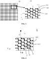
- the rectangular region 20 includes: multiple active regions 101 that are separate from one another and located on a substrate (not shown in the figure), multiple connecting pads 102 and multiple MTJs 103.
- multiple separate active regions 101 may be formed in a semiconductor substrate.
- the semiconductor substrate includes a silicon substrate, a silicon on insulator (SOI) substrate, a gallium nitride substrate, silicon carbide, gallium carbide, etc.
- SOI silicon on insulator
- the active regions 101 may be formed on the semiconductor substrate by a patterning process, and trench isolating structures are formed between the active regions 101.
- multiple active regions 101 in the semiconductor substrate are distributed in an array at equal intervals.
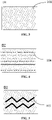
- the multiple active regions 101 are strip-shaped, and extend in a third direction C.
- the semiconductor substrate includes connecting pads 102.
- Each connecting pad 102 includes a first part 1021 and a second part 1022.
- Each of the first part 1021 and the second part 1022 is connected to end parts of respective adjacent active regions 101.
- the first part 1021 extends in a first direction A
- the second part 1022 extends in a second direction B.
- the first part 1021 and the second part 1022 may each have an end connected to the same end part of the same active region 101, and the other end of the first part 1021 and the other end of the second part 1022 are respectively connected to the end parts of different active regions 101.
- the connecting pads 102 are located above the active regions 101 distributed in an array.
- the first part 1021 and the second part 1022 of the connecting pad 102 are strip-shaped.
- the first part 1021 of the connecting pad 102 extends in a first direction A, and the two ends of the first part 1021 are respectively connected to the end part of the active region 101 with a sign 2 and the end of the active region 101 with a sign 3.
- the second part 1022 of the connecting pad 102 extends in a second direction B, and the two ends of the second part 1022 are respectively connected to the end part of the active region 101 with a sign 1 and the end of the active region 101 with a sign 2.
- an included angle ⁇ between the second direction B and the third direction C may be an acute angle, and the included angle may specifically range from 15° to 35°.
- An included angle ⁇ between the first direction A and the second direction B may be 90°.
- the included angle ⁇ between the first direction A and the second direction B may also be less than 90°, and the implementation and principle are the same and will not be described again.
- the connecting pads extend in a stair shape.
- the connecting pad connecting the end parts of three adjacent active regions 101 form a stair unit, and multiple stair units are connected to form connecting pads extending in a stair shape.
- the first part 1021 and the second part 1022 form a stair unit, and multiple stair units on multiple active regions are connected to form connecting pads in a stair shape.
- the active regions are distributed in a staggered array.
- the first part 1021 is connected to the end parts of the adjacent active regions 101 in different columns, and the second part 1022 is connected to end parts of the adjacent active regions 101 in the same column.
- Each MTJ 103 may be connected to a respective connecting pad 102.
- a single connecting pad 102 may be connected to multiple MTJs 103.
- each MTJ 103 is disposed above the space between two bent parts formed by the connecting pads 102 extending in a stair shape, and is connected to the connecting pad 102.
- the MTJs 103 may be disposed above the middle points of the first part 1021 and the second part 1022 of the connecting pad 102 respectively and are connected to the first part 1021 and the second part 1022 of the connecting pad 102 respectively.
- multiple MTJs 103 may be distributed in an array in the first direction A and the second direction B.
- the distance between each adjacent rows of MTJs 103 in the first direction A is the same, and the distance between each adjacent columns of MTJs 103 in the second direction B is the same.
- MTJs 103 may be connected to the end parts of multiple active regions 101 connected to the connecting pad 102.
- the end parts of the active region 101 may be a source electrode or a drain electrode of a transistor (the transistor may be a Negative-channel Metal Oxide Semiconductor (NMOS) transistor).
- NMOS Negative-channel Metal Oxide Semiconductor
- FIG. 1 and FIG. 2 illustrate schematic structural diagrams of the semiconductor structure 1.
- structures such as word lines, bit lines and selection lines also need to be provided for realizing the control over the MTJs 103.
- the layered design structure of the semiconductor structure 1 provided in the embodiments of the present invention is described below with reference to FIG. 3 to FIG. 8.
- FIG. 3 to FIG. 8 are also depicted with the rectangular region 20 of the semiconductor structure 1 in FIG. 1 as an example.
- FIG. 3 illustrates a schematic structural diagram of a layer D1 of a semiconductor structure provided in the present invention.
- multiple separate active regions 101 are arranged at intervals, and the description of the active regions 101 may refer to the description of FIG. 1 and FIG. 2 .
- multiple separate active regions 101 may be formed in a silicon substrate by a patterning method.
- the patterning method includes, but is not limited to, semiconductor manufacturing processes such as self-aligned double patterning (SADP) and self-aligned quadruple patterning (SAQP). Trench isolating structures are formed between the active regions 101.
- SADP self-aligned double patterning
- SAQP self-aligned quadruple patterning
- FIG. 4 illustrates a schematic structural diagram of a layer D2 of a semiconductor structure provided in the present invention.
- Multiple word lines 104 are disposed in parallel in the layer D2 as shown in FIG. 4 , and the word lines 104 are configured to control the transistors connected to the MTJs 103.
- the word lines 104 at the layer D2 may be disposed above the layer D1.
- the word lines 104 at the layer D2 may also be arranged to pass through the active region 101 at the layer D1.
- a single active region 101 may be divided into two end parts and a middle part by two adjacent word lines 104. Specifically, the active region 101 and the two word lines 104 passing therethrough form two transistors (MOS transistors).
- the two transistors share the same source electrode.
- the middle part of the active region 101 is the source electrode shared by the two transistors, and the two end parts of the active region 101 are drain electrodes of the two transistors respectively.
- the two transistors share the same drain electrode.
- the middle part of the active region 101 is the drain electrode shared by the two transistors, and the two end parts of the active region 101 are source electrodes of the two transistors respectively.
- the word lines 104 may be buried gate lines.
- the word lines 104 may extend in the first direction A, and a single word line 104 may pass through multiple active regions 101.
- FIG. 5 illustrates a schematic structural diagram of a layer D3 of a semiconductor structure provided in the present invention.
- Multiple selection lines 105 are provided in the layer D3 as shown in FIG. 5 .
- the selection lines 105 may be polylines and may extend in the same direction as the word lines 104. As an example, the selection lines 105 may extend in the first direction A.
- the layer D3 may be disposed above the layer D1, and the selection lines 105 may be connected to the middle parts of respective active regions 101 through contact plugs.
- a middle part of an active region 101 is a shared source electrode or a shared drain electrode of two transistors, and the selection line 105 may be connected to the shared source electrode or the shared drain electrode of the two transistors through a contact plug.
- a first plug 107 may be located between the layer D1 and the layer D3, and the middle part of the active region 101 may be connected to the selection line 105 by the first plug 107.
- a single selection line 105 may be connected to the middle parts of multiple active regions 101.
- FIG. 6 illustrates a schematic structural diagram of a layer D4 of a semiconductor structure provided in the present invention. Multiple connecting pads 102 are provided in the layer D4 as shown in FIG. 6 , and the description of the connecting pads 102 may refer to the description of FIG. 1 and FIG. 2 .
- FIG. 10 illustrates a schematic structural diagram of second plugs provided in the present invention according to an embodiment.
- the second plugs 108 are located between the layer D1 and the layer D4.
- One end of a second plug 108 is connected to an end part of an active region 101, and the other end of the second plug 108 is connected to a connecting pad 102.
- the first plugs 107 may have a smaller height than the second plug 108, so that the bit lines 105 are located below the connecting pads 102 so that the subsequent connection of the MTJs 103 is not disturbed.
- the first plugs 107 may have a greater height than the second plugs 108.
- FIG. 7 illustrates a schematic structural diagram of a layer D5 of a semiconductor structure provided in the present invention.
- Multiple MTJs 103 are provided in the layer D5 as shown in FIG. 7 .
- the MTJs 103 are located above the connecting pads 102 and are connected to the connecting pads 102.
- An MTJ 103 includes a free layer, a fixed layer and a tunnel barrier, and stores information by directions of magnetic polarization of the free layer and the fixed layer.
- the resistance when the directions of magnetic polarization of the free layer and the fixed layer are in a parallel state, the resistance is low, which represents the information "1"; and when the directions of magnetic polarization of the free layer and the fixed layer are in an antiparallel state, the resistance is high, which represents the information "0".
- FIG. 8 illustrates a schematic structural diagram of a layer D6 of a semiconductor structure provided in the present invention.
- Multiple bit lines 106 are provided in the layer D6 as shown in FIG. 8 , and the bit lines 106 extend in the second direction B.
- 11 bit lines may be correspondingly provided in the layer D6, and each bit line 106 is configured to connect the upper ends of a row of MTJs 103 in the second direction B as shown in FIG. 1 and FIG. 2 .
- FIG. 11 illustrates a schematic structural diagram of a layer D3 of a semiconductor structure according to another embodiment provided in the present invention.
- Multiple selection lines 105 are provided in the layer D3 as shown in FIG. 11 .
- the selection lines 105 are straight lines, and extend in a direction perpendicular to a direction in which the word lines 104 extend.
- the selection lines 105 may extend in the second direction B, and a single selection line 105 may be connected to the middle parts of the active regions 101 in the same column.
- the structures of the layer D1, the layer D2, the layer D4, the layer D5 and the layer D6 are the same as those in the previous embodiment, and will not be described again.
- the selection lines 105 may be connected to the active regions 101 by first plugs.
- FIG. 12 illustrates a schematic structural diagram of first plugs according to another embodiment provided in the present invention. As shown in FIG. 12 , the first plugs 107 are located between the layer D1 and the layer D3, and the middle parts of the active regions 101 may be connected to the selection lines 105 by the first plugs 107. Specifically, the middle parts of the active regions 101 in the same column may be connected to the same selection line 105. The connecting pad 102 may be connected to the end parts of the adjacent active regions 101 by second plugs.
- FIG. 13 illustrates a schematic structural diagram of second plugs according to another embodiment provided in the present invention. As shown in FIG. 13 , the second plugs 108 are located between the layer D1 and the layer D4. One end of a second plug 108 is connected to an end part of an active region 101, and the other end of the second plug 108 is connected to the connecting pad 102.
- the first plugs 107 may have a height equal to that of the second plugs 108.
- the layer D3 and the layer D4 may be located at the same layer.
- the first plugs 107 and the second plugs 108 may be formed in the same process step.
- a conductive material may be simultaneously formed in first through holes for preparing the first plugs and second through holes for preparing the second plugs, so as to form the first plugs and the second plugs.
- the conductive material may be at least one of TiN, W, TaN, Co, AL, WN, polysilicon and silicon germanide.
- a memory cell including: a transistor, and a memory structure. One end of the transistor is connected to one end of the memory structure. The other end of the transistor, a gate electrode of the transistor, the other end of the memory structure, and the end of the transistor connected to the memory structure are respectively used as a first end, a second end, a third end and a fourth end of the memory cell.
- a metal oxide semiconductor (MOS) transistor includes a gate electrode 2, and two ends of the MOS transistor are respectively a source electrode and a drain electrode. When one end of the MOS transistor is a source electrode, the other end of the MOS transistor is a drain electrode; or when one end of the MOS transistor is a drain electrode, the other end of the MOS transistor is a source electrode.
- the transistor may be an NMOS transistor or a PMOS transistor.
- a memory structure 5 may include at least one of: a magnetic tunnel junction (MTJ), a capacitive memory structure, a resistive memory structure and a phase change memory structure.
- the MTJ may include a free layer, a fixed layer and a tunnel barrier.
- the fixed layer of the MTJ is connected to the source electrode of the MOS transistor.
- the free layer of the MTJ may be used as the third end 3 of the memory cell.
- the drain electrode of the MOS transistor may be used as the first end 1 of the memory cell.
- the gate electrode of the MOS transistor may be used as the second end 2 of the memory cell.
- the source electrode of the MOS transistor connected to the fixed layer of the MTJ may be used as the fourth end 4 of the memory cell.
- the memory array includes M ⁇ N memory cells forming an array of M rows and N columns. Both M and the N are positive integers greater than or equal to 2.
- the memory array further includes M bit lines in one-to-one correspondence to the M rows of memory cells. Third ends of memory cells in each of the M rows are all connected to a corresponding one of the M bit lines.
- the memory array further includes N word lines in one-to-one correspondence to the N columns of memory cells. Second ends of memory cells in each of the N columns are all connected to a corresponding one of the N word lines.
- a fourth end of a memory cell in an X th row and Y th column is connected to a fourth end of a memory cell in a P th row a Q th column, X is equal to P minus A, and Y is equal to Q minus B
- M ⁇ N memory cells form an array of M rows and N columns, and both M and N are positive integers greater than or equal to 2.
- M bit lines (BL) are BL[1] to BL[M] respectively.
- the M bit lines are in one-to-one correspondence to M rows of memory cells.
- Third ends 3 of the memory cells in the same row are all connected to the corresponding bit lines BL.
- the third ends 3 of the memory cells in first row are all connected to the bit lines BL[1] in the first row
- the third ends 3 of the memory cells in the X th row are all connected to the bit lines BL[X] in the X th row.
- N word lines WL are respectively WL[1] to WL[N].
- the N word lines are in one-to-one correspondence to the N columns of memory cells.
- Second ends 2 of the memory cells in the same column are all connected to the corresponding word lines WL.
- the second ends 2 of the memory cells in the first column are all connected to the word lines WL[1] in the first column
- the second ends 2 of the memory cells in the X th column are all connected to the word lines WL[X] in the X th column.
- the fourth end 4 of the memory cell in the X th row and Y th column is connected to the fourth end 4 of the memory cell in the P th row and Q th column.
- X is equal to P minus A
- Y is equal to Q minus B.
- A is equal to B.
- the fourth end 4 of the memory cell in the X th row and Y th column is connected to the fourth end 4 of the memory cell in the (X+B) th row and (Y+B) th column.
- B may be any integer such as 1, 2 and 3.
- the fourth end 4 of the memory cell in the tenth row and tenth column is connected to the fourth end 4 of the memory cell in the eleventh row and eleventh column, or the fourth end 4 of the memory cell in the tenth row and tenth column is connected to the fourth end 4 of the memory cell in the twelfth row and twelfth column.
- N selection lines SL are in one-to-one correspondence to the N columns of memory cells. Frst ends 1 of the memory cells in the same column are connected to the corresponding selection lines SL. As shown in FIG. 15 , the first ends 1 of the memory cells in the first column are connected to the selection line SL[1] in the first column, and the first ends 1 of the memory cells in the Y th column is connected to the selection line SL[Y] in the Y th column.
- the fourth ends 4 of all memory cells are connected together.
- a and B are equal to 1
- the fourth end 4 of the memory cell in the M th row and first column are connected together.
- the fourth end 4 of the memory cell in the (M-1) th row and second column are all connected together.
- FIG. 16 illustrates a schematic diagram of control levels of MTJs provided in the present invention.
- the memory structure 5 is an MTJ
- the MTJ in the memory cell in the i th row and j th column is marked as M ij .
- bit line BL[i] in the i th row connected to the MTJ M ij is set to a high level, and the other bit lines BL[others] are set to a low level; and word lines WL[j-k] to WL[j+k] in the (j-k) th column to the (j+k) th column are set to a high level, and the other word lines WL[others] are set to a low level; and selection lines SL are all set to a low level.
- bit lines BL are all set to a low level; word lines WL[j-k] to WL[j+k] in the (j-k) th column to the (j+k) th column are set to a high level, and the other word lines WL[others] are set to a low level; and selection lines SL[j-k] to SL[j+k] in the (j-k) th column to the (j+k) th column corresponding to WL[j-k] to WL[j+k] are set to a high level, and the other selection lines SL[others] are set to a low level.
- the bit line BL[i] in the i th row connected to the MTJ M ij is set to a high level, and the other bit lines BL[others] are set to a low level' word lines WL[j-k] to WL[j+k] in the (j-k) th column to the (j+k) th column are set to a high level, and other word lines WL[others] are set to a low level; and selection lines SL are all set to a low level.
- the number of transistors operating the same MTJ M ij is j+k-(j-k)+1, that is, 2k+1 transistors operate one MTJ.
- the present invention by connecting transistors connected to multiple memory structures, the purpose of driving the same memory structure by multiple transistors can be realized, and it is also ensured that the memory density is not reduced.
Landscapes
- Engineering & Computer Science (AREA)
- Computer Hardware Design (AREA)
- Microelectronics & Electronic Packaging (AREA)
- Mram Or Spin Memory Techniques (AREA)
- Hall/Mr Elements (AREA)
- Semiconductor Memories (AREA)
Abstract
Description
- This application claims priority to
Chinese Patent Application No. 202011475752.5, filed with the China National Intellectual Administration on December 15, 2020 - The present invention relates to the field of semiconductor technologies, and particularly relates to a semiconductor structure, a memory cell and a memory array.
- A Magnetoresistive Random Access Memory (MRAM) is a non-volatile magnetic random access memory which has the characteristics of higher reading and writing speed, higher integration level and more repeated reading and writing times, and is widely used in current devices such as computers.
- In the related art, Magnetic Tunnel Junctions (MTJs) are specifically used to read, write and store information ("0" or "1") in the MRAM, and each MTJ can be driven by multiple transistors to increase the driving current in driving the MTJ. The MRAM in which one MTJ is driven by n transistors can also be called nT-MRAM. However, multiple transistors will occupy a larger area and reduce the memory density.
- This present invention provides a semiconductor structure, a memory cell and a memory array. An nT-MRAM can be realized by a relatively simple structure. Transistors connected to multiple MTJs are connected by connecting pads, thereby realizing the purpose of driving the same MTJ by n transistors without reducing the memory density.
- The present invention provides a semiconductor structure, including: active regions that are separate from one another and located on a substrate; connecting pads, wherein each of the connecting pads includes a first part and a second part, each of the first part and the second part is connected to end parts of respective adjacent ones of the active regions, the first part extends in a first direction, and the second part extends in a second direction; and magnetic tunnel junctions (MTJs), wherein each of the MTJs is connected to a respective one of the connecting pads.
- Optionally, the first part and the second part are connected to a same end part of one of the active regions.
- Optionally, the connecting pads extend in a stair shape.
- Optionally, the active regions are strip-shaped and extend in a third direction.
- Optionally, the semiconductor structure further includes word lines passing through the active regions, wherein two of the word lines divide one of the active regions into two end parts of the active region and a middle part of the active region.
- Optionally, the semiconductor structure further includes: selection lines, wherein each of the selection lines is connected to middle parts of respective active regions.
- Optionally, the selection lines are polylines, and extend in a same direction as the word lines.
- Optionally, the semiconductor structure further includes: first plugs connecting the middle parts of the active regions to the selection lines; and second plugs connecting the end parts of the active regions to the connecting pads, wherein the first plugs have a smaller height than the second plugs.
- Optionally, the selection lines are straight lines, and extend in a direction perpendicular to a direction in which the word lines extend.
- Optionally, the semiconductor structure further includes: first plugs connecting the middle parts of the active regions to the selection lines; and second plugs connecting the end parts of the active regions to the connecting pads, wherein the first plugs have a same height as the second plugs.
- Optionally, the first plugs and the second plugs are formed in a same process step.
- Optionally, the semiconductor structure further includes: bit lines, wherein each of the bit lines is connected to respective MTJs and extend in the second direction.
- Optionally, an included angle between the second direction and the third direction ranges from 15° to 35°.
- The present invention further provides a memory cell, including a transistor, and a memory structure, wherein one end of the transistor is connected to one end of the memory structure; and the other end of the transistor, a gate electrode of the transistor, the other end of the memory structure, and the end of the transistor connected to the memory structure are respectively used as a first end, a second end, a third end and a fourth end of the memory cell.
- Optionally, the memory structure includes at least one of: a magnetic tunnel junction (MTJ), a capacitive memory structure, a resistive memory structure or a phase change memory structure.
- The present invention further provides a memory array, including: M∗N memory cells forming an array of M rows and N columns, wherein both M and the N are positive integers greater than or equal to 2; M bit lines in one-to-one correspondence to the M rows of memory cells, wherein third ends of memory cells in each of the M rows are all connected to a corresponding one of the M bit lines; and N word lines in one-to-one correspondence to the N columns of memory cells, wherein second ends of memory cells in each of the N columns are all connected to a corresponding one of the N word lines, wherein a fourth end of a memory cell in an Xth row and Yth column is connected to a fourth end of a memory cell in a Pth row a Qth column, X is equal to P minus A, and Y is equal to Q minus B.
- Optionally, A is equal to B.
- Optionally, both A and B are equal to 1.
- Optionally, the memory array further includes: N selection lines in one-to-one correspondence to the N columns of memory cells, and first ends of memory cells in each of the N columns are connected to a corresponding one of the N selection lines.
- Optionally, among the M∗N memory cells, fourth ends of all memory cells, between which a distance in a row direction is A and a distance in a column direction is B, are connected together.
- In conclusion, in the semiconductor structure provided in the present invention, multiple transistors are connected by connecting pads, so that one MTJ can be driven by n transistors without reducing the memory density.
- In order to more clearly illustrate the technical solutions in the embodiments of this application, the drawings to be used in the embodiments or in description of the prior art will be briefly introduced below. It is apparent that the drawings in the following description are only some of the embodiments of this application, and those skilled in the art can obtain other drawings according to these drawings without creative efforts.
-
FIG. 1 illustrates a schematic structural diagram of a semiconductor structure according to an embodiment provided in the present invention. -
FIG. 2 illustrates a schematic diagram of extension directions of a semiconductor structure provided in the present invention. -
FIG. 3 illustrates a schematic structural diagram of a layer D1 of a semiconductor structure provided in the present invention. -
FIG. 4 illustrates a schematic structural diagram of a layer D2 of a semiconductor structure provided in the present invention. -
FIG. 5 illustrates a schematic structural diagram of a layer D3 of a semiconductor structure provided in the present invention. -
FIG. 6 illustrates a schematic structural diagram of a layer D4 of a semiconductor structure provided in the present invention. -
FIG. 7 illustrates a schematic structural diagram of a layer D5 of a semiconductor structure provided in the present invention. -
FIG. 8 illustrates a schematic structural diagram of a layer D6 of a semiconductor structure provided in the present invention. -
FIG. 9 illustrates a schematic structural diagram of first plugs according to an embodiment provided in the present invention. -
FIG. 10 illustrates a schematic structural diagram of second plugs according to an embodiment provided in the present invention. -
FIG. 11 illustrates a schematic structural diagram of a layer D3 of a semiconductor structure according to another embodiment provided in the present invention. -
FIG. 12 illustrates a schematic structural diagram of first plugs according to another embodiment provided in the present invention. -
FIG. 13 illustrates a schematic structural diagram of second plugs according to another embodiment provided in the present invention. -
FIG. 14 illustrates a schematic diagram of a memory cell provided in the present invention. -
FIG. 15 illustrates a schematic diagram of a memory array provided in the present invention. -
FIG. 16 illustrates a schematic diagram of control levels of MTJs provided in the present invention. - The technical solutions in the embodiments of the present invention will be clearly and completely described below with reference to the drawings in the embodiments of the present invention. It is apparent that the described embodiments are only a part of the embodiments of present invention, but are not all of the embodiments. All other embodiments obtained by those of ordinary skill in the art based on the embodiments of the present invention without creative efforts shall fall within the scope of protection of present invention.
- The terms "first", "second", "third", "fourth", etc. (if any) in the description, claims and the above drawings of the specification are used to distinguish similar objects, and are not used to describe a specific order or a sequential order. It should be understood that the data used in this way can be interchanged under appropriate conditions, so that the embodiments of the present invention described herein can be implemented in a sequence other than those illustrated or described herein. In addition, the terms "include", "comprise" and any other variations thereof are intended to cover the non-exclusive inclusion. For example, a process, method, system, product, or device that includes a series of steps or units is not necessarily limited to those expressly listed steps or units, but may include other steps or units not expressly listed or inherent to such a process, method, product, or device.
- The present invention provides a semiconductor structure. As illustrated in
FIG. 1 , thesemiconductor structure 1 includes a memory array. The memory array includes multiple magnetic tunnel junctions (MTJs). The multiple MTJs can be arranged in rows and columns in an array, and each MTJ may be used for reading and writing of information. InFIG. 1 , taking anyrectangular region 20 in thesemiconductor structure 1 as an example, therectangular region 20 includes: multipleactive regions 101 that are separate from one another and located on a substrate (not shown in the figure), multiple connectingpads 102 andmultiple MTJs 103. - As an example, multiple separate
active regions 101 may be formed in a semiconductor substrate. The semiconductor substrate includes a silicon substrate, a silicon on insulator (SOI) substrate, a gallium nitride substrate, silicon carbide, gallium carbide, etc. Specifically, theactive regions 101 may be formed on the semiconductor substrate by a patterning process, and trench isolating structures are formed between theactive regions 101. - Referring to
FIG. 2 , multipleactive regions 101 in the semiconductor substrate (not shown in the figure) are distributed in an array at equal intervals. Specifically, the multipleactive regions 101 are strip-shaped, and extend in a third direction C. - The semiconductor substrate includes connecting
pads 102. Each connectingpad 102 includes afirst part 1021 and asecond part 1022. Each of thefirst part 1021 and thesecond part 1022 is connected to end parts of respective adjacentactive regions 101. Thefirst part 1021 extends in a first direction A, and thesecond part 1022 extends in a second direction B. Thefirst part 1021 and thesecond part 1022 may each have an end connected to the same end part of the sameactive region 101, and the other end of thefirst part 1021 and the other end of thesecond part 1022 are respectively connected to the end parts of differentactive regions 101. - Specifically, as illustrated in
FIG. 2 , the connectingpads 102 are located above theactive regions 101 distributed in an array. Thefirst part 1021 and thesecond part 1022 of the connectingpad 102 are strip-shaped. Thefirst part 1021 of the connectingpad 102 extends in a first direction A, and the two ends of thefirst part 1021 are respectively connected to the end part of theactive region 101 with asign ② and the end of theactive region 101 with asign ③. Thesecond part 1022 of the connectingpad 102 extends in a second direction B, and the two ends of thesecond part 1022 are respectively connected to the end part of theactive region 101 with asign ① and the end of theactive region 101 with asign ②. In such a case, the same end part of theactive region 101 with thesign ② may be connected to thefirst part 1021 and thesecond part 1022 respectively. An included angle β between the second direction B and the third direction C may be an acute angle, and the included angle may specifically range from 15° to 35°. An included angle α between the first direction A and the second direction B may be 90°. Exemplarily, in other possible implementations, the included angle α between the first direction A and the second direction B may also be less than 90°, and the implementation and principle are the same and will not be described again. - Optionally, the connecting pads extend in a stair shape. Specifically, the connecting pad connecting the end parts of three adjacent
active regions 101 form a stair unit, and multiple stair units are connected to form connecting pads extending in a stair shape. Specifically, referring toFIG. 2 , thefirst part 1021 and thesecond part 1022 form a stair unit, and multiple stair units on multiple active regions are connected to form connecting pads in a stair shape. - Optionally, as shown in
FIG. 2 , the active regions are distributed in a staggered array. Thefirst part 1021 is connected to the end parts of the adjacentactive regions 101 in different columns, and thesecond part 1022 is connected to end parts of the adjacentactive regions 101 in the same column. - Each
MTJ 103 may be connected to a respective connectingpad 102. As an example, a single connectingpad 102 may be connected tomultiple MTJs 103. InFIG. 1 , taking therectangular region 20 including 39MTJs 103 distributed in 14 rows and 11 columns as an example, eachMTJ 103 is disposed above the space between two bent parts formed by the connectingpads 102 extending in a stair shape, and is connected to the connectingpad 102. Specifically, theMTJs 103 may be disposed above the middle points of thefirst part 1021 and thesecond part 1022 of the connectingpad 102 respectively and are connected to thefirst part 1021 and thesecond part 1022 of the connectingpad 102 respectively. - Optionally, as shown in
FIG. 2 ,multiple MTJs 103 may be distributed in an array in the first direction A and the second direction B. The distance between each adjacent rows ofMTJs 103 in the first direction A is the same, and the distance between each adjacent columns ofMTJs 103 in the second direction B is the same. - Through s connecting
pad 102,MTJs 103 may be connected to the end parts of multipleactive regions 101 connected to the connectingpad 102. The end parts of theactive region 101 may be a source electrode or a drain electrode of a transistor (the transistor may be a Negative-channel Metal Oxide Semiconductor (NMOS) transistor). In such a case, asingle MTJ 103 may be driven by multiple transistors together. -
FIG. 1 and FIG. 2 illustrate schematic structural diagrams of thesemiconductor structure 1. In order to realize the functions of thesemiconductor structure 1, structures such as word lines, bit lines and selection lines also need to be provided for realizing the control over theMTJs 103. The layered design structure of thesemiconductor structure 1 provided in the embodiments of the present invention is described below with reference toFIG. 3 to FIG. 8. FIG. 3 to FIG. 8 are also depicted with therectangular region 20 of thesemiconductor structure 1 inFIG. 1 as an example. - First layer (D1):
FIG. 3 illustrates a schematic structural diagram of a layer D1 of a semiconductor structure provided in the present invention. In the layer D1 as shown inFIG. 3 , multiple separateactive regions 101 are arranged at intervals, and the description of theactive regions 101 may refer to the description ofFIG. 1 and FIG. 2 . Specifically, multiple separateactive regions 101 may be formed in a silicon substrate by a patterning method. The patterning method includes, but is not limited to, semiconductor manufacturing processes such as self-aligned double patterning (SADP) and self-aligned quadruple patterning (SAQP). Trench isolating structures are formed between theactive regions 101. - Second layer (D2):
FIG. 4 illustrates a schematic structural diagram of a layer D2 of a semiconductor structure provided in the present invention. Multiple word lines 104 are disposed in parallel in the layer D2 as shown inFIG. 4 , and the word lines 104 are configured to control the transistors connected to theMTJs 103. As an example, the word lines 104 at the layer D2 may be disposed above the layer D1. In another example, the word lines 104 at the layer D2 may also be arranged to pass through theactive region 101 at the layer D1. A singleactive region 101 may be divided into two end parts and a middle part by two adjacent word lines 104. Specifically, theactive region 101 and the twoword lines 104 passing therethrough form two transistors (MOS transistors). The two transistors share the same source electrode. The middle part of theactive region 101 is the source electrode shared by the two transistors, and the two end parts of theactive region 101 are drain electrodes of the two transistors respectively. Alternatively, the two transistors share the same drain electrode. The middle part of theactive region 101 is the drain electrode shared by the two transistors, and the two end parts of theactive region 101 are source electrodes of the two transistors respectively. In an example, the word lines 104 may be buried gate lines. - Optionally, the word lines 104 may extend in the first direction A, and a
single word line 104 may pass through multipleactive regions 101. - Third layer (D3):
FIG. 5 illustrates a schematic structural diagram of a layer D3 of a semiconductor structure provided in the present invention.Multiple selection lines 105 are provided in the layer D3 as shown inFIG. 5 . The selection lines 105 may be polylines and may extend in the same direction as the word lines 104. As an example, theselection lines 105 may extend in the first direction A. The layer D3 may be disposed above the layer D1, and theselection lines 105 may be connected to the middle parts of respectiveactive regions 101 through contact plugs. Specifically, a middle part of anactive region 101 is a shared source electrode or a shared drain electrode of two transistors, and theselection line 105 may be connected to the shared source electrode or the shared drain electrode of the two transistors through a contact plug. As shown inFIG. 9 , afirst plug 107 may be located between the layer D1 and the layer D3, and the middle part of theactive region 101 may be connected to theselection line 105 by thefirst plug 107. Asingle selection line 105 may be connected to the middle parts of multipleactive regions 101. - Fourth layer (D4):
FIG. 6 illustrates a schematic structural diagram of a layer D4 of a semiconductor structure provided in the present invention. Multiple connectingpads 102 are provided in the layer D4 as shown inFIG. 6 , and the description of the connectingpads 102 may refer to the description ofFIG. 1 and FIG. 2 . - Optionally, the connecting
pads 102 may be connected to the end parts of theactive regions 101 by second plugs.FIG. 10 illustrates a schematic structural diagram of second plugs provided in the present invention according to an embodiment. As shown inFIG. 10 , thesecond plugs 108 are located between the layer D1 and the layer D4. One end of asecond plug 108 is connected to an end part of anactive region 101, and the other end of thesecond plug 108 is connected to a connectingpad 102. With reference toFIG. 9 and FIG. 10 , thefirst plugs 107 may have a smaller height than thesecond plug 108, so that thebit lines 105 are located below the connectingpads 102 so that the subsequent connection of theMTJs 103 is not disturbed. In other examples, thefirst plugs 107 may have a greater height than the second plugs 108. - Fifth layer (D5):
FIG. 7 illustrates a schematic structural diagram of a layer D5 of a semiconductor structure provided in the present invention.Multiple MTJs 103 are provided in the layer D5 as shown inFIG. 7 . As an example, theMTJs 103 are located above the connectingpads 102 and are connected to the connectingpads 102. AnMTJ 103 includes a free layer, a fixed layer and a tunnel barrier, and stores information by directions of magnetic polarization of the free layer and the fixed layer. For example, when the directions of magnetic polarization of the free layer and the fixed layer are in a parallel state, the resistance is low, which represents the information "1"; and when the directions of magnetic polarization of the free layer and the fixed layer are in an antiparallel state, the resistance is high, which represents the information "0". - Sixth layer (D6):
FIG. 8 illustrates a schematic structural diagram of a layer D6 of a semiconductor structure provided in the present invention.Multiple bit lines 106 are provided in the layer D6 as shown inFIG. 8 , and thebit lines 106 extend in the second direction B. For example, for the 11 columns ofMTJs 103 distributed inFIG. 1 ,11 bit lines may be correspondingly provided in the layer D6, and eachbit line 106 is configured to connect the upper ends of a row ofMTJs 103 in the second direction B as shown inFIG. 1 and FIG. 2 . - Optionally, the present invention further provides another semiconductor structure which may be used as an equivalent replacement of the
semiconductor structure 1 provided inFIG. 3 to FIG. 8 .FIG. 11 illustrates a schematic structural diagram of a layer D3 of a semiconductor structure according to another embodiment provided in the present invention.Multiple selection lines 105 are provided in the layer D3 as shown inFIG. 11 . The selection lines 105 are straight lines, and extend in a direction perpendicular to a direction in which the word lines 104 extend. As an example, theselection lines 105 may extend in the second direction B, and asingle selection line 105 may be connected to the middle parts of theactive regions 101 in the same column. The structures of the layer D1, the layer D2, the layer D4, the layer D5 and the layer D6 are the same as those in the previous embodiment, and will not be described again. - Optionally, the
selection lines 105 may be connected to theactive regions 101 by first plugs.FIG. 12 illustrates a schematic structural diagram of first plugs according to another embodiment provided in the present invention. As shown inFIG. 12 , thefirst plugs 107 are located between the layer D1 and the layer D3, and the middle parts of theactive regions 101 may be connected to theselection lines 105 by the first plugs 107. Specifically, the middle parts of theactive regions 101 in the same column may be connected to thesame selection line 105. The connectingpad 102 may be connected to the end parts of the adjacentactive regions 101 by second plugs.FIG. 13 illustrates a schematic structural diagram of second plugs according to another embodiment provided in the present invention. As shown inFIG. 13 , thesecond plugs 108 are located between the layer D1 and the layer D4. One end of asecond plug 108 is connected to an end part of anactive region 101, and the other end of thesecond plug 108 is connected to the connectingpad 102. - Optionally, with reference to
FIG. 12 and FIG. 13 , thefirst plugs 107 may have a height equal to that of the second plugs 108. In such a case, the layer D3 and the layer D4 may be located at the same layer. As an example, thefirst plugs 107 and thesecond plugs 108 may be formed in the same process step. For example, a conductive material may be simultaneously formed in first through holes for preparing the first plugs and second through holes for preparing the second plugs, so as to form the first plugs and the second plugs. The conductive material may be at least one of TiN, W, TaN, Co, AL, WN, polysilicon and silicon germanide. - Another embodiment of the present invention provides a memory cell, including: a transistor, and a memory structure. One end of the transistor is connected to one end of the memory structure. The other end of the transistor, a gate electrode of the transistor, the other end of the memory structure, and the end of the transistor connected to the memory structure are respectively used as a first end, a second end, a third end and a fourth end of the memory cell.
- As shown in
FIG. 14 , a metal oxide semiconductor (MOS) transistor includes agate electrode 2, and two ends of the MOS transistor are respectively a source electrode and a drain electrode. When one end of the MOS transistor is a source electrode, the other end of the MOS transistor is a drain electrode; or when one end of the MOS transistor is a drain electrode, the other end of the MOS transistor is a source electrode. The transistor may be an NMOS transistor or a PMOS transistor. - Optionally, a
memory structure 5 may include at least one of: a magnetic tunnel junction (MTJ), a capacitive memory structure, a resistive memory structure and a phase change memory structure. As an example, when thememory structure 5 is an MTJ, the MTJ may include a free layer, a fixed layer and a tunnel barrier. Specifically, the fixed layer of the MTJ is connected to the source electrode of the MOS transistor. The free layer of the MTJ may be used as thethird end 3 of the memory cell. The drain electrode of the MOS transistor may be used as thefirst end 1 of the memory cell. The gate electrode of the MOS transistor may be used as thesecond end 2 of the memory cell. The source electrode of the MOS transistor connected to the fixed layer of the MTJ may be used as thefourth end 4 of the memory cell. - Another embodiment of the present invention provides a memory array. The memory array includes M∗N memory cells forming an array of M rows and N columns. Both M and the N are positive integers greater than or equal to 2. The memory array further includes M bit lines in one-to-one correspondence to the M rows of memory cells. Third ends of memory cells in each of the M rows are all connected to a corresponding one of the M bit lines. The memory array further includes N word lines in one-to-one correspondence to the N columns of memory cells. Second ends of memory cells in each of the N columns are all connected to a corresponding one of the N word lines. A fourth end of a memory cell in an Xth row and Yth column is connected to a fourth end of a memory cell in a Pth row a Qth column, X is equal to P minus A, and Y is equal to Q minus B
- As shown in
FIG. 15 , M∗N memory cells form an array of M rows and N columns, and both M and N are positive integers greater than or equal to 2. M bit lines (BL) are BL[1] to BL[M] respectively. The M bit lines are in one-to-one correspondence to M rows of memory cells. Third ends 3 of the memory cells in the same row are all connected to the corresponding bit lines BL. For example, the third ends 3 of the memory cells in first row are all connected to the bit lines BL[1] in the first row, and the third ends 3 of the memory cells in the Xth row are all connected to the bit lines BL[X] in the Xth row. N word lines WL are respectively WL[1] to WL[N]. The N word lines are in one-to-one correspondence to the N columns of memory cells. Second ends 2 of the memory cells in the same column are all connected to the corresponding word lines WL. For example, the second ends 2 of the memory cells in the first column are all connected to the word lines WL[1] in the first column, and the second ends 2 of the memory cells in the Xth column are all connected to the word lines WL[X] in the Xth column. Thefourth end 4 of the memory cell in the Xth row and Yth column is connected to thefourth end 4 of the memory cell in the Pth row and Qth column. X is equal to P minus A, and Y is equal to Q minus B. - As an example, A is equal to B. Specifically, the
fourth end 4 of the memory cell in the Xth row and Yth column is connected to thefourth end 4 of the memory cell in the (X+B)th row and (Y+B)th column. B may be any integer such as 1, 2 and 3. For example, thefourth end 4 of the memory cell in the tenth row and tenth column is connected to thefourth end 4 of the memory cell in the eleventh row and eleventh column, or thefourth end 4 of the memory cell in the tenth row and tenth column is connected to thefourth end 4 of the memory cell in the twelfth row and twelfth column. - Optionally, N selection lines SL are in one-to-one correspondence to the N columns of memory cells. Frst ends 1 of the memory cells in the same column are connected to the corresponding selection lines SL. As shown in
FIG. 15 , the first ends 1 of the memory cells in the first column are connected to the selection line SL[1] in the first column, and the first ends 1 of the memory cells in the Yth column is connected to the selection line SL[Y] in the Yth column. - Optionally, among the M∗N memory cells, the fourth ends 4 of all memory cells, between which a distance in a row direction is A and a distance in a column direction is B, are connected together. For example, when both A and B are equal to 1, the
fourth end 4 of the memory cell in the Mth row and first column, thefourth end 4 of the memory cell in the (M-1)th row and second column, thefourth end 4 of the memory cell in the (M-2)th row and third column ... are all connected together. -
FIG. 16 illustrates a schematic diagram of control levels of MTJs provided in the present invention. As an example, when thememory structure 5 is an MTJ, the MTJ in the memory cell in the ith row and jth column is marked as Mij. When writing information "1" (WRITE1) through the MTJ Mij, the bit line BL[i] in the ith row connected to the MTJ Mij is set to a high level, and the other bit lines BL[others] are set to a low level; and word lines WL[j-k] to WL[j+k] in the (j-k)th column to the (j+k)th column are set to a high level, and the other word lines WL[others] are set to a low level; and selection lines SL are all set to a low level. When writing information "0" (WRITE0) through the MTJ Mij, bit lines BL are all set to a low level; word lines WL[j-k] to WL[j+k] in the (j-k)th column to the (j+k)th column are set to a high level, and the other word lines WL[others] are set to a low level; and selection lines SL[j-k] to SL[j+k] in the (j-k)th column to the (j+k)th column corresponding to WL[j-k] to WL[j+k] are set to a high level, and the other selection lines SL[others] are set to a low level. When reading information (READ) from the MTJ Mij, the bit line BL[i] in the ith row connected to the MTJ Mij is set to a high level, and the other bit lines BL[others] are set to a low level' word lines WL[j-k] to WL[j+k] in the (j-k)th column to the (j+k)th column are set to a high level, and other word lines WL[others] are set to a low level; and selection lines SL are all set to a low level. In this example, the number of transistors operating the same MTJ Mij is j+k-(j-k)+1, that is, 2k+1 transistors operate one MTJ. - In the present invention, by connecting transistors connected to multiple memory structures, the purpose of driving the same memory structure by multiple transistors can be realized, and it is also ensured that the memory density is not reduced.
- The above embodiments only serve to illustrate the technical solutions of the present invention, but are not limited thereto. Although the embodiments of the present invention are described in detail with reference to the above embodiments, it should be understood by those skilled in the art that the technical solutions described in the foregoing embodiments may be modified, or some or all of the technical features may be equivalently replaced. However, the essence of the corresponding technical solutions resulting from these modifications or replacements does not depart from the scope of the technical solutions of the embodiments of the present invention.
Claims (20)
- A semiconductor structure, comprising:active regions that are separate from one another and located on a substrate;connecting pads, wherein each of the connecting pads comprises a first part and a second part, each of the first part and the second part is connected to end parts of respective adjacent ones of the active regions, the first part extends in a first direction, and the second part extends in a second direction; andmagnetic tunnel junctions (MTJs), wherein each of the MTJs is connected to a respective one of the connecting pads.
- The semiconductor structure of claim 1, wherein
the first part and the second part are connected to a same end part of one of the active regions. - The semiconductor structure of claim 2, wherein
the connecting pads extend in a stair shape. - The semiconductor structure of claim 1, wherein
the active regions are strip-shaped and extend in a third direction. - The semiconductor structure of claim 4, further comprising:
word lines passing through the active regions, wherein two of the word lines divide one of the active regions into two end parts of the active region and a middle part of the active region. - The semiconductor structure of claim 5, further comprising:
selection lines, wherein each of the selection lines is connected to middle parts of respective active regions. - The semiconductor structure of claim 6, wherein
the selection lines are polylines, and extend in a same direction as the word lines. - The semiconductor structure of claim 7, further comprising:first plugs connecting the middle parts of the active regions to the selection lines; andsecond plugs connecting the end parts of the active regions to the connecting pads, wherein the first plugs have a smaller height than the second plugs.
- The semiconductor structure of claim 6, wherein
the selection lines are straight lines, and extend in a direction perpendicular to a direction in which the word lines extend. - The semiconductor structure of claim 9, further comprising:first plugs connecting the middle parts of the active regions to the selection lines; andsecond plugs connecting the end parts of the active regions to the connecting pads, wherein the first plugs have a same height as the second plugs.
- The semiconductor structure of claim 10, wherein
the first plugs and the second plugs are formed in a same process step. - The semiconductor structure of claim 1, further comprising:
bit lines, wherein each of the bit lines is connected to respective MTJs and extend in the second direction. - The semiconductor structure of claim 4, wherein
an included angle between the second direction and the third direction ranges from 15° to 35°. - A memory cell, comprising:a transistor, anda memory structure,wherein one end of the transistor is connected to one end of the memory structure; andthe other end of the transistor, a gate electrode of the transistor, the other end of the memory structure, and the end of the transistor connected to the memory structure are respectively used as a first end, a second end, a third end and a fourth end of the memory cell.
- The memory cell of claim 14, wherein the memory structure comprises at least one of:a magnetic tunnel junction (MTJ),a capacitive memory structure,a resistive memory structure, ora phase change memory structure.
- A memory array, comprising:M∗N memory cells of claim 14 forming an array of M rows and N columns, wherein both M and the N are positive integers greater than or equal to 2;M bit lines in one-to-one correspondence to the M rows of memory cells, wherein third ends of memory cells in each of the M rows are all connected to a corresponding one of the M bit lines; andN word lines in one-to-one correspondence to the N columns of memory cells, wherein second ends of memory cells in each of the N columns are all connected to a corresponding one of the N word lines, wherein a fourth end of a memory cell in an Xth row and Yth column is connected to a fourth end of a memory cell in a Pth row a Qth column, X is equal to P minus A, and Y is equal to Q minus B.
- The memory array of claim 16, wherein
A is equal to B. - The memory array of claim 17, wherein
both A and B are equal to 1. - The memory array of claim 16, further comprising:
N selection lines in one-to-one correspondence to the N columns of memory cells, and first ends of memory cells in each of the N columns are connected to a corresponding one of the N selection lines. - The memory array of claim 16, wherein among the M∗N memory cells, fourth ends of all memory cells, between which a distance in a row direction is A and a distance in a column direction is B, are connected together.
Applications Claiming Priority (2)
| Application Number | Priority Date | Filing Date | Title |
|---|---|---|---|
| CN202011475752.5A CN114639773A (en) | 2020-12-15 | 2020-12-15 | Semiconductor structure, memory unit and memory array |
| PCT/CN2021/095445 WO2022127027A1 (en) | 2020-12-15 | 2021-05-24 | Semiconductor structure, memory cell, and memory array |
Publications (3)
| Publication Number | Publication Date |
|---|---|
| EP4044240A1 true EP4044240A1 (en) | 2022-08-17 |
| EP4044240A4 EP4044240A4 (en) | 2023-01-11 |
| EP4044240B1 EP4044240B1 (en) | 2026-04-29 |
Family
ID=80952402
Family Applications (1)
| Application Number | Title | Priority Date | Filing Date |
|---|---|---|---|
| EP21843572.5A Active EP4044240B1 (en) | 2020-12-15 | 2021-05-24 | Semiconductor structure for a memory |
Country Status (4)
| Country | Link |
|---|---|
| US (1) | US12108682B2 (en) |
| EP (1) | EP4044240B1 (en) |
| CN (1) | CN114639773A (en) |
| WO (1) | WO2022127027A1 (en) |
Families Citing this family (1)
| Publication number | Priority date | Publication date | Assignee | Title |
|---|---|---|---|---|
| CN115132777B (en) * | 2022-08-31 | 2022-11-25 | 睿力集成电路有限公司 | Semiconductor structure, forming method thereof and memory |
Family Cites Families (18)
| Publication number | Priority date | Publication date | Assignee | Title |
|---|---|---|---|---|
| KR100399436B1 (en) | 2001-03-28 | 2003-09-29 | 주식회사 하이닉스반도체 | A Magnetic random access memory and a method for manufacturing the same |
| JP2008130995A (en) * | 2006-11-24 | 2008-06-05 | Toshiba Corp | Semiconductor memory device |
| JP2011228443A (en) * | 2010-04-19 | 2011-11-10 | Toshiba Corp | Semiconductor memory, and method of manufacturing the same |
| US8587982B2 (en) * | 2011-02-25 | 2013-11-19 | Qualcomm Incorporated | Non-volatile memory array configurable for high performance and high density |
| JP5677186B2 (en) * | 2011-05-06 | 2015-02-25 | 株式会社東芝 | Semiconductor memory device |
| JP5677187B2 (en) | 2011-05-09 | 2015-02-25 | 株式会社東芝 | Semiconductor memory device |
| JP2012256690A (en) * | 2011-06-08 | 2012-12-27 | Toshiba Corp | Semiconductor storage device |
| KR101962784B1 (en) * | 2012-10-09 | 2019-03-27 | 삼성전자주식회사 | semiconductor memory device having discriminatory read and write operations according to temperature |
| US10170185B2 (en) | 2013-12-24 | 2019-01-01 | Intel Corporation | Hybrid memory and MTJ based MRAM bit-cell and array |
| KR102124209B1 (en) * | 2014-04-14 | 2020-06-18 | 삼성전자주식회사 | Semiconductor memory device |
| US9659623B1 (en) * | 2016-03-28 | 2017-05-23 | Nxp Usa, Inc. | Memory having a plurality of resistive non-volatile memory cells |
| CN108630249B (en) * | 2017-03-24 | 2022-03-04 | 铠侠股份有限公司 | Semiconductor memory device with a plurality of memory cells |
| WO2019005129A1 (en) | 2017-06-30 | 2019-01-03 | Intel Corporation | Spin hall effect magnetic random-access memory bitcell |
| US10497415B2 (en) * | 2018-01-08 | 2019-12-03 | Spin Memory, Inc. | Dual gate memory devices |
| US10516096B2 (en) | 2018-03-28 | 2019-12-24 | Globalfoundries Singapore Pte. Ltd. | Magnetic random access memory structures, integrated circuits, and methods for fabricating the same |
| US10861524B1 (en) * | 2019-12-11 | 2020-12-08 | Nxp Usa, Inc. | Magnetoresistive random access memory (MRAM) with OTP cells |
| CN111489777B (en) * | 2020-04-15 | 2023-11-10 | 上海新微技术研发中心有限公司 | Magnetic memory structure, array, read-write control method and preparation method |
| CN212136451U (en) * | 2020-06-19 | 2020-12-11 | 长鑫存储技术有限公司 | Memory device |
-
2020
- 2020-12-15 CN CN202011475752.5A patent/CN114639773A/en active Pending
-
2021
- 2021-05-24 EP EP21843572.5A patent/EP4044240B1/en active Active
- 2021-05-24 WO PCT/CN2021/095445 patent/WO2022127027A1/en not_active Ceased
- 2021-07-27 US US17/386,455 patent/US12108682B2/en active Active
Also Published As
| Publication number | Publication date |
|---|---|
| WO2022127027A1 (en) | 2022-06-23 |
| EP4044240A4 (en) | 2023-01-11 |
| EP4044240B1 (en) | 2026-04-29 |
| CN114639773A (en) | 2022-06-17 |
| US12108682B2 (en) | 2024-10-01 |
| US20220190236A1 (en) | 2022-06-16 |
Similar Documents
| Publication | Publication Date | Title |
|---|---|---|
| US9184218B2 (en) | Semiconductor memory device having three-dimensional cross point array | |
| US10229929B2 (en) | Semiconductor memory devices including protrusion pads | |
| US8878271B2 (en) | Vertical access device and apparatuses having a body connection line, and related method of operating the same | |
| CN102365628B (en) | Technology for providing semiconductor memory device | |
| US20220108988A1 (en) | Conductive line contact regions having multiple multi-direction conductive lines and staircase conductive line contact structures for semiconductor devices | |
| KR20020015971A (en) | Mram arrangement | |
| US11696432B2 (en) | Multi-direction conductive line and staircase contact for semiconductor devices | |
| KR102320645B1 (en) | A memory cell comprising a transistor having a GaP channel material | |
| US11587931B2 (en) | Multiplexor for a semiconductor device | |
| US12302545B2 (en) | Thin film transistor random access memory | |
| US20220359540A1 (en) | Thin film transistor random access memory | |
| EP3958319B1 (en) | Memory, forming method therefor and control method therefor | |
| US10411071B2 (en) | Semiconductor storage device | |
| US12052858B2 (en) | Vertical contacts for semiconductor devices | |
| WO2023091862A1 (en) | Deck selection layouts in a memory device | |
| EP4044240B1 (en) | Semiconductor structure for a memory | |
| EP4044239B1 (en) | Semiconductor structure and storage circuit | |
| US11348972B1 (en) | Semiconductor structure and manufacturing method thereof | |
| US11380387B1 (en) | Multiplexor for a semiconductor device | |
| US11791260B2 (en) | Contacts for twisted conductive lines within memory arrays | |
| US20250221024A1 (en) | Semiconductor device, method for designing the same, and method for manufacturing the same | |
| US10510392B1 (en) | Integrated circuits having memory cells with shared bit lines and shared source lines | |
| CN113497082A (en) | Magnetic random access memory architecture | |
| US20260128097A1 (en) | Memory Circuitry And Methods Used In Forming Memory Circuitry | |
| CN117998837A (en) | Semiconductor structure and method for forming the same, and memory |
Legal Events
| Date | Code | Title | Description |
|---|---|---|---|
| STAA | Information on the status of an ep patent application or granted ep patent |
Free format text: STATUS: UNKNOWN |
|
| STAA | Information on the status of an ep patent application or granted ep patent |
Free format text: STATUS: THE INTERNATIONAL PUBLICATION HAS BEEN MADE |
|
| PUAI | Public reference made under article 153(3) epc to a published international application that has entered the european phase |
Free format text: ORIGINAL CODE: 0009012 |
|
| STAA | Information on the status of an ep patent application or granted ep patent |
Free format text: STATUS: REQUEST FOR EXAMINATION WAS MADE |
|
| 17P | Request for examination filed |
Effective date: 20220124 |
|
| AK | Designated contracting states |
Kind code of ref document: A1 Designated state(s): AL AT BE BG CH CY CZ DE DK EE ES FI FR GB GR HR HU IE IS IT LI LT LU LV MC MK MT NL NO PL PT RO RS SE SI SK SM TR |
|
| A4 | Supplementary search report drawn up and despatched |
Effective date: 20221209 |
|
| RIC1 | Information provided on ipc code assigned before grant |
Ipc: G11C 11/02 20060101ALI20221205BHEP Ipc: H01L 27/22 20060101AFI20221205BHEP |
|
| DAV | Request for validation of the european patent (deleted) | ||
| DAX | Request for extension of the european patent (deleted) | ||
| STAA | Information on the status of an ep patent application or granted ep patent |
Free format text: STATUS: EXAMINATION IS IN PROGRESS |
|
| 17Q | First examination report despatched |
Effective date: 20250411 |
|
| REG | Reference to a national code |
Ref country code: DE Ipc: H10B0063100000 Ref country code: DE Ref legal event code: R079 Ref document number: 602021053312 Country of ref document: DE Free format text: PREVIOUS MAIN CLASS: H01L0027220000 Ipc: H10B0063100000 |
|
| REG | Reference to a national code |
Ref country code: DE Free format text: PREVIOUS MAIN CLASS: H10B0063100000 Ref country code: DE Ref legal event code: R079 Ref document number: 602021053312 Country of ref document: DE Free format text: PREVIOUS MAIN CLASS: H10B0063100000 Ipc: H10B0061000000 |
|
| RIC1 | Information provided on ipc code assigned before grant |
Ipc: H10B 63/10 20230101AFI20251127BHEP Ipc: G11C 11/02 20060101ALI20251127BHEP |
|
| RIC1 | Information provided on ipc code assigned before grant |
Ipc: H10B 61/00 20230101AFI20251223BHEP Ipc: G11C 11/16 20060101ALI20251223BHEP |
|
| GRAP | Despatch of communication of intention to grant a patent |
Free format text: ORIGINAL CODE: EPIDOSNIGR1 |
|
| STAA | Information on the status of an ep patent application or granted ep patent |
Free format text: STATUS: GRANT OF PATENT IS INTENDED |
|
| GRAS | Grant fee paid |
Free format text: ORIGINAL CODE: EPIDOSNIGR3 |
|
| INTG | Intention to grant announced |
Effective date: 20260224 |
|
| GRAA | (expected) grant |
Free format text: ORIGINAL CODE: 0009210 |
|
| STAA | Information on the status of an ep patent application or granted ep patent |
Free format text: STATUS: THE PATENT HAS BEEN GRANTED |
|
| P01 | Opt-out of the competence of the unified patent court (upc) registered |
Free format text: CASE NUMBER: UPC_APP_0009184_4044240/2026 Effective date: 20260310 |
|
| AK | Designated contracting states |
Kind code of ref document: B1 Designated state(s): AL AT BE BG CH CY CZ DE DK EE ES FI FR GB GR HR HU IE IS IT LI LT LU LV MC MK MT NL NO PL PT RO RS SE SI SK SM TR |
|
| REG | Reference to a national code |
Ref country code: CH Ref legal event code: F10 Free format text: ST27 STATUS EVENT CODE: U-0-0-F10-F00 (AS PROVIDED BY THE NATIONAL OFFICE) Effective date: 20260429 Ref country code: GB Ref legal event code: FG4D |
|
| REG | Reference to a national code |
Ref country code: DE Ref legal event code: R096 Ref document number: 602021053312 Country of ref document: DE |