EP4044161A1 - Display panel and display device - Google Patents
Display panel and display device Download PDFInfo
- Publication number
- EP4044161A1 EP4044161A1 EP21787846.1A EP21787846A EP4044161A1 EP 4044161 A1 EP4044161 A1 EP 4044161A1 EP 21787846 A EP21787846 A EP 21787846A EP 4044161 A1 EP4044161 A1 EP 4044161A1
- Authority
- EP
- European Patent Office
- Prior art keywords
- unit
- transistor
- terminal
- display
- reset
- Prior art date
- Legal status (The legal status is an assumption and is not a legal conclusion. Google has not performed a legal analysis and makes no representation as to the accuracy of the status listed.)
- Pending
Links
- 230000037361 pathway Effects 0.000 claims description 119
- 239000003990 capacitor Substances 0.000 claims description 27
- 238000004080 punching Methods 0.000 claims description 12
- 238000002955 isolation Methods 0.000 claims description 10
- 108010001267 Protein Subunits Proteins 0.000 claims description 4
- 230000000694 effects Effects 0.000 abstract description 12
- 238000004088 simulation Methods 0.000 description 4
- 230000000007 visual effect Effects 0.000 description 3
- 230000002159 abnormal effect Effects 0.000 description 2
- 230000009286 beneficial effect Effects 0.000 description 1
- 238000000034 method Methods 0.000 description 1
- 230000009466 transformation Effects 0.000 description 1
Images


Classifications
-
- G—PHYSICS
- G09—EDUCATION; CRYPTOGRAPHY; DISPLAY; ADVERTISING; SEALS
- G09G—ARRANGEMENTS OR CIRCUITS FOR CONTROL OF INDICATING DEVICES USING STATIC MEANS TO PRESENT VARIABLE INFORMATION
- G09G3/00—Control arrangements or circuits, of interest only in connection with visual indicators other than cathode-ray tubes
- G09G3/20—Control arrangements or circuits, of interest only in connection with visual indicators other than cathode-ray tubes for presentation of an assembly of a number of characters, e.g. a page, by composing the assembly by combination of individual elements arranged in a matrix no fixed position being assigned to or needed to be assigned to the individual characters or partial characters
- G09G3/22—Control arrangements or circuits, of interest only in connection with visual indicators other than cathode-ray tubes for presentation of an assembly of a number of characters, e.g. a page, by composing the assembly by combination of individual elements arranged in a matrix no fixed position being assigned to or needed to be assigned to the individual characters or partial characters using controlled light sources
- G09G3/30—Control arrangements or circuits, of interest only in connection with visual indicators other than cathode-ray tubes for presentation of an assembly of a number of characters, e.g. a page, by composing the assembly by combination of individual elements arranged in a matrix no fixed position being assigned to or needed to be assigned to the individual characters or partial characters using controlled light sources using electroluminescent panels
- G09G3/32—Control arrangements or circuits, of interest only in connection with visual indicators other than cathode-ray tubes for presentation of an assembly of a number of characters, e.g. a page, by composing the assembly by combination of individual elements arranged in a matrix no fixed position being assigned to or needed to be assigned to the individual characters or partial characters using controlled light sources using electroluminescent panels semiconductive, e.g. using light-emitting diodes [LED]
- G09G3/3208—Control arrangements or circuits, of interest only in connection with visual indicators other than cathode-ray tubes for presentation of an assembly of a number of characters, e.g. a page, by composing the assembly by combination of individual elements arranged in a matrix no fixed position being assigned to or needed to be assigned to the individual characters or partial characters using controlled light sources using electroluminescent panels semiconductive, e.g. using light-emitting diodes [LED] organic, e.g. using organic light-emitting diodes [OLED]
- G09G3/3225—Control arrangements or circuits, of interest only in connection with visual indicators other than cathode-ray tubes for presentation of an assembly of a number of characters, e.g. a page, by composing the assembly by combination of individual elements arranged in a matrix no fixed position being assigned to or needed to be assigned to the individual characters or partial characters using controlled light sources using electroluminescent panels semiconductive, e.g. using light-emitting diodes [LED] organic, e.g. using organic light-emitting diodes [OLED] using an active matrix
-
- G—PHYSICS
- G09—EDUCATION; CRYPTOGRAPHY; DISPLAY; ADVERTISING; SEALS
- G09G—ARRANGEMENTS OR CIRCUITS FOR CONTROL OF INDICATING DEVICES USING STATIC MEANS TO PRESENT VARIABLE INFORMATION
- G09G3/00—Control arrangements or circuits, of interest only in connection with visual indicators other than cathode-ray tubes
- G09G3/20—Control arrangements or circuits, of interest only in connection with visual indicators other than cathode-ray tubes for presentation of an assembly of a number of characters, e.g. a page, by composing the assembly by combination of individual elements arranged in a matrix no fixed position being assigned to or needed to be assigned to the individual characters or partial characters
- G09G3/22—Control arrangements or circuits, of interest only in connection with visual indicators other than cathode-ray tubes for presentation of an assembly of a number of characters, e.g. a page, by composing the assembly by combination of individual elements arranged in a matrix no fixed position being assigned to or needed to be assigned to the individual characters or partial characters using controlled light sources
- G09G3/30—Control arrangements or circuits, of interest only in connection with visual indicators other than cathode-ray tubes for presentation of an assembly of a number of characters, e.g. a page, by composing the assembly by combination of individual elements arranged in a matrix no fixed position being assigned to or needed to be assigned to the individual characters or partial characters using controlled light sources using electroluminescent panels
- G09G3/32—Control arrangements or circuits, of interest only in connection with visual indicators other than cathode-ray tubes for presentation of an assembly of a number of characters, e.g. a page, by composing the assembly by combination of individual elements arranged in a matrix no fixed position being assigned to or needed to be assigned to the individual characters or partial characters using controlled light sources using electroluminescent panels semiconductive, e.g. using light-emitting diodes [LED]
-
- G—PHYSICS
- G09—EDUCATION; CRYPTOGRAPHY; DISPLAY; ADVERTISING; SEALS
- G09G—ARRANGEMENTS OR CIRCUITS FOR CONTROL OF INDICATING DEVICES USING STATIC MEANS TO PRESENT VARIABLE INFORMATION
- G09G3/00—Control arrangements or circuits, of interest only in connection with visual indicators other than cathode-ray tubes
- G09G3/20—Control arrangements or circuits, of interest only in connection with visual indicators other than cathode-ray tubes for presentation of an assembly of a number of characters, e.g. a page, by composing the assembly by combination of individual elements arranged in a matrix no fixed position being assigned to or needed to be assigned to the individual characters or partial characters
- G09G3/22—Control arrangements or circuits, of interest only in connection with visual indicators other than cathode-ray tubes for presentation of an assembly of a number of characters, e.g. a page, by composing the assembly by combination of individual elements arranged in a matrix no fixed position being assigned to or needed to be assigned to the individual characters or partial characters using controlled light sources
- G09G3/30—Control arrangements or circuits, of interest only in connection with visual indicators other than cathode-ray tubes for presentation of an assembly of a number of characters, e.g. a page, by composing the assembly by combination of individual elements arranged in a matrix no fixed position being assigned to or needed to be assigned to the individual characters or partial characters using controlled light sources using electroluminescent panels
- G09G3/32—Control arrangements or circuits, of interest only in connection with visual indicators other than cathode-ray tubes for presentation of an assembly of a number of characters, e.g. a page, by composing the assembly by combination of individual elements arranged in a matrix no fixed position being assigned to or needed to be assigned to the individual characters or partial characters using controlled light sources using electroluminescent panels semiconductive, e.g. using light-emitting diodes [LED]
- G09G3/3208—Control arrangements or circuits, of interest only in connection with visual indicators other than cathode-ray tubes for presentation of an assembly of a number of characters, e.g. a page, by composing the assembly by combination of individual elements arranged in a matrix no fixed position being assigned to or needed to be assigned to the individual characters or partial characters using controlled light sources using electroluminescent panels semiconductive, e.g. using light-emitting diodes [LED] organic, e.g. using organic light-emitting diodes [OLED]
- G09G3/3225—Control arrangements or circuits, of interest only in connection with visual indicators other than cathode-ray tubes for presentation of an assembly of a number of characters, e.g. a page, by composing the assembly by combination of individual elements arranged in a matrix no fixed position being assigned to or needed to be assigned to the individual characters or partial characters using controlled light sources using electroluminescent panels semiconductive, e.g. using light-emitting diodes [LED] organic, e.g. using organic light-emitting diodes [OLED] using an active matrix
- G09G3/3233—Control arrangements or circuits, of interest only in connection with visual indicators other than cathode-ray tubes for presentation of an assembly of a number of characters, e.g. a page, by composing the assembly by combination of individual elements arranged in a matrix no fixed position being assigned to or needed to be assigned to the individual characters or partial characters using controlled light sources using electroluminescent panels semiconductive, e.g. using light-emitting diodes [LED] organic, e.g. using organic light-emitting diodes [OLED] using an active matrix with pixel circuitry controlling the current through the light-emitting element
-
- G—PHYSICS
- G09—EDUCATION; CRYPTOGRAPHY; DISPLAY; ADVERTISING; SEALS
- G09F—DISPLAYING; ADVERTISING; SIGNS; LABELS OR NAME-PLATES; SEALS
- G09F9/00—Indicating arrangements for variable information in which the information is built-up on a support by selection or combination of individual elements
- G09F9/30—Indicating arrangements for variable information in which the information is built-up on a support by selection or combination of individual elements in which the desired character or characters are formed by combining individual elements
- G09F9/302—Indicating arrangements for variable information in which the information is built-up on a support by selection or combination of individual elements in which the desired character or characters are formed by combining individual elements characterised by the form or geometrical disposition of the individual elements
-
- G—PHYSICS
- G09—EDUCATION; CRYPTOGRAPHY; DISPLAY; ADVERTISING; SEALS
- G09F—DISPLAYING; ADVERTISING; SIGNS; LABELS OR NAME-PLATES; SEALS
- G09F9/00—Indicating arrangements for variable information in which the information is built-up on a support by selection or combination of individual elements
- G09F9/30—Indicating arrangements for variable information in which the information is built-up on a support by selection or combination of individual elements in which the desired character or characters are formed by combining individual elements
- G09F9/33—Indicating arrangements for variable information in which the information is built-up on a support by selection or combination of individual elements in which the desired character or characters are formed by combining individual elements being semiconductor devices, e.g. diodes
-
- G—PHYSICS
- G09—EDUCATION; CRYPTOGRAPHY; DISPLAY; ADVERTISING; SEALS
- G09G—ARRANGEMENTS OR CIRCUITS FOR CONTROL OF INDICATING DEVICES USING STATIC MEANS TO PRESENT VARIABLE INFORMATION
- G09G3/00—Control arrangements or circuits, of interest only in connection with visual indicators other than cathode-ray tubes
- G09G3/20—Control arrangements or circuits, of interest only in connection with visual indicators other than cathode-ray tubes for presentation of an assembly of a number of characters, e.g. a page, by composing the assembly by combination of individual elements arranged in a matrix no fixed position being assigned to or needed to be assigned to the individual characters or partial characters
- G09G3/22—Control arrangements or circuits, of interest only in connection with visual indicators other than cathode-ray tubes for presentation of an assembly of a number of characters, e.g. a page, by composing the assembly by combination of individual elements arranged in a matrix no fixed position being assigned to or needed to be assigned to the individual characters or partial characters using controlled light sources
- G09G3/30—Control arrangements or circuits, of interest only in connection with visual indicators other than cathode-ray tubes for presentation of an assembly of a number of characters, e.g. a page, by composing the assembly by combination of individual elements arranged in a matrix no fixed position being assigned to or needed to be assigned to the individual characters or partial characters using controlled light sources using electroluminescent panels
-
- G—PHYSICS
- G09—EDUCATION; CRYPTOGRAPHY; DISPLAY; ADVERTISING; SEALS
- G09G—ARRANGEMENTS OR CIRCUITS FOR CONTROL OF INDICATING DEVICES USING STATIC MEANS TO PRESENT VARIABLE INFORMATION
- G09G3/00—Control arrangements or circuits, of interest only in connection with visual indicators other than cathode-ray tubes
- G09G3/20—Control arrangements or circuits, of interest only in connection with visual indicators other than cathode-ray tubes for presentation of an assembly of a number of characters, e.g. a page, by composing the assembly by combination of individual elements arranged in a matrix no fixed position being assigned to or needed to be assigned to the individual characters or partial characters
- G09G3/22—Control arrangements or circuits, of interest only in connection with visual indicators other than cathode-ray tubes for presentation of an assembly of a number of characters, e.g. a page, by composing the assembly by combination of individual elements arranged in a matrix no fixed position being assigned to or needed to be assigned to the individual characters or partial characters using controlled light sources
- G09G3/30—Control arrangements or circuits, of interest only in connection with visual indicators other than cathode-ray tubes for presentation of an assembly of a number of characters, e.g. a page, by composing the assembly by combination of individual elements arranged in a matrix no fixed position being assigned to or needed to be assigned to the individual characters or partial characters using controlled light sources using electroluminescent panels
- G09G3/32—Control arrangements or circuits, of interest only in connection with visual indicators other than cathode-ray tubes for presentation of an assembly of a number of characters, e.g. a page, by composing the assembly by combination of individual elements arranged in a matrix no fixed position being assigned to or needed to be assigned to the individual characters or partial characters using controlled light sources using electroluminescent panels semiconductive, e.g. using light-emitting diodes [LED]
- G09G3/3208—Control arrangements or circuits, of interest only in connection with visual indicators other than cathode-ray tubes for presentation of an assembly of a number of characters, e.g. a page, by composing the assembly by combination of individual elements arranged in a matrix no fixed position being assigned to or needed to be assigned to the individual characters or partial characters using controlled light sources using electroluminescent panels semiconductive, e.g. using light-emitting diodes [LED] organic, e.g. using organic light-emitting diodes [OLED]
-
- G—PHYSICS
- G09—EDUCATION; CRYPTOGRAPHY; DISPLAY; ADVERTISING; SEALS
- G09G—ARRANGEMENTS OR CIRCUITS FOR CONTROL OF INDICATING DEVICES USING STATIC MEANS TO PRESENT VARIABLE INFORMATION
- G09G2300/00—Aspects of the constitution of display devices
- G09G2300/04—Structural and physical details of display devices
- G09G2300/0404—Matrix technologies
- G09G2300/0413—Details of dummy pixels or dummy lines in flat panels
-
- G—PHYSICS
- G09—EDUCATION; CRYPTOGRAPHY; DISPLAY; ADVERTISING; SEALS
- G09G—ARRANGEMENTS OR CIRCUITS FOR CONTROL OF INDICATING DEVICES USING STATIC MEANS TO PRESENT VARIABLE INFORMATION
- G09G2300/00—Aspects of the constitution of display devices
- G09G2300/04—Structural and physical details of display devices
- G09G2300/0421—Structural details of the set of electrodes
- G09G2300/043—Compensation electrodes or other additional electrodes in matrix displays related to distortions or compensation signals, e.g. for modifying TFT threshold voltage in column driver
-
- G—PHYSICS
- G09—EDUCATION; CRYPTOGRAPHY; DISPLAY; ADVERTISING; SEALS
- G09G—ARRANGEMENTS OR CIRCUITS FOR CONTROL OF INDICATING DEVICES USING STATIC MEANS TO PRESENT VARIABLE INFORMATION
- G09G2300/00—Aspects of the constitution of display devices
- G09G2300/08—Active matrix structure, i.e. with use of active elements, inclusive of non-linear two terminal elements, in the pixels together with light emitting or modulating elements
- G09G2300/0809—Several active elements per pixel in active matrix panels
-
- G—PHYSICS
- G09—EDUCATION; CRYPTOGRAPHY; DISPLAY; ADVERTISING; SEALS
- G09G—ARRANGEMENTS OR CIRCUITS FOR CONTROL OF INDICATING DEVICES USING STATIC MEANS TO PRESENT VARIABLE INFORMATION
- G09G2300/00—Aspects of the constitution of display devices
- G09G2300/08—Active matrix structure, i.e. with use of active elements, inclusive of non-linear two terminal elements, in the pixels together with light emitting or modulating elements
- G09G2300/0809—Several active elements per pixel in active matrix panels
- G09G2300/0819—Several active elements per pixel in active matrix panels used for counteracting undesired variations, e.g. feedback or autozeroing
-
- G—PHYSICS
- G09—EDUCATION; CRYPTOGRAPHY; DISPLAY; ADVERTISING; SEALS
- G09G—ARRANGEMENTS OR CIRCUITS FOR CONTROL OF INDICATING DEVICES USING STATIC MEANS TO PRESENT VARIABLE INFORMATION
- G09G2300/00—Aspects of the constitution of display devices
- G09G2300/08—Active matrix structure, i.e. with use of active elements, inclusive of non-linear two terminal elements, in the pixels together with light emitting or modulating elements
- G09G2300/0809—Several active elements per pixel in active matrix panels
- G09G2300/0842—Several active elements per pixel in active matrix panels forming a memory circuit, e.g. a dynamic memory with one capacitor
-
- G—PHYSICS
- G09—EDUCATION; CRYPTOGRAPHY; DISPLAY; ADVERTISING; SEALS
- G09G—ARRANGEMENTS OR CIRCUITS FOR CONTROL OF INDICATING DEVICES USING STATIC MEANS TO PRESENT VARIABLE INFORMATION
- G09G2300/00—Aspects of the constitution of display devices
- G09G2300/08—Active matrix structure, i.e. with use of active elements, inclusive of non-linear two terminal elements, in the pixels together with light emitting or modulating elements
- G09G2300/0809—Several active elements per pixel in active matrix panels
- G09G2300/0842—Several active elements per pixel in active matrix panels forming a memory circuit, e.g. a dynamic memory with one capacitor
- G09G2300/0852—Several active elements per pixel in active matrix panels forming a memory circuit, e.g. a dynamic memory with one capacitor being a dynamic memory with more than one capacitor
-
- G—PHYSICS
- G09—EDUCATION; CRYPTOGRAPHY; DISPLAY; ADVERTISING; SEALS
- G09G—ARRANGEMENTS OR CIRCUITS FOR CONTROL OF INDICATING DEVICES USING STATIC MEANS TO PRESENT VARIABLE INFORMATION
- G09G2310/00—Command of the display device
- G09G2310/02—Addressing, scanning or driving the display screen or processing steps related thereto
- G09G2310/0232—Special driving of display border areas
-
- G—PHYSICS
- G09—EDUCATION; CRYPTOGRAPHY; DISPLAY; ADVERTISING; SEALS
- G09G—ARRANGEMENTS OR CIRCUITS FOR CONTROL OF INDICATING DEVICES USING STATIC MEANS TO PRESENT VARIABLE INFORMATION
- G09G2310/00—Command of the display device
- G09G2310/06—Details of flat display driving waveforms
- G09G2310/061—Details of flat display driving waveforms for resetting or blanking
-
- G—PHYSICS
- G09—EDUCATION; CRYPTOGRAPHY; DISPLAY; ADVERTISING; SEALS
- G09G—ARRANGEMENTS OR CIRCUITS FOR CONTROL OF INDICATING DEVICES USING STATIC MEANS TO PRESENT VARIABLE INFORMATION
- G09G2320/00—Control of display operating conditions
- G09G2320/02—Improving the quality of display appearance
- G09G2320/0233—Improving the luminance or brightness uniformity across the screen
-
- G—PHYSICS
- G09—EDUCATION; CRYPTOGRAPHY; DISPLAY; ADVERTISING; SEALS
- G09G—ARRANGEMENTS OR CIRCUITS FOR CONTROL OF INDICATING DEVICES USING STATIC MEANS TO PRESENT VARIABLE INFORMATION
- G09G2320/00—Control of display operating conditions
- G09G2320/06—Adjustment of display parameters
- G09G2320/0686—Adjustment of display parameters with two or more screen areas displaying information with different brightness or colours
-
- G—PHYSICS
- G09—EDUCATION; CRYPTOGRAPHY; DISPLAY; ADVERTISING; SEALS
- G09G—ARRANGEMENTS OR CIRCUITS FOR CONTROL OF INDICATING DEVICES USING STATIC MEANS TO PRESENT VARIABLE INFORMATION
- G09G2354/00—Aspects of interface with display user
Definitions
- the present application relates to the field of display technology, and in particular, to a display panel and a display device.
- a full-screen can greatly improve the visual effect of users, so the full-screen has attracted extensive attention.
- a special-shaped area is usually set on the front of the display device.
- the special-shaped area is configured to install a camera, earpiece, fingerprint identification sensor, or physical keys.
- the load and number of pixels will be changed by setting the special-shaped area on the display device, which resulting in uneven pixel display, and further resulting in abnormal display.
- the present application provides a display panel and a display device, which is configured to improve the display effect.
- the first aspect is provided by the present disclosure is a display panel, includes a first area and a second area, including a plurality of first pixel rows, the second area includes a plurality of second pixel rows, and each of the first pixel row and the second pixel row include a plurality of pixels, the number of the pixels of each first pixel row is greater than the number of the pixels of each second pixel row; wherein the plurality of pixels of the first pixel row are a plurality of display pixels, and the plurality of the pixels of the second pixel row are a plurality of display pixels and a plurality of virtual pixels;each of the plurality of display pixels includes a display pixel circuit, each of the plurality of virtual pixels includes a virtual pixel circuit, the virtual pixel circuit includes a compensation unit, and the virtual pixel circuit is configured to compensate the display pixel circuits of one of the plurality of second pixel rows when the display pixel circuits of the one of the plurality of second pixel rows are reset;
- each of the display pixel circuit and the virtual pixel circuit includes: a writing unit, configured to receive a first scanning signal; a driving unit, wherein the driving unit is connected to the writing unit by a driving node, and the writing unit is driven by the first scanning signal to write a data signal to the driving node in a writing stage; a control unit, configured to receive an enable signal, and wherein the control unit is connected to the driving unit, so that the driving unit is connected to a power signal line by the control unit; a reset unit, configured to receive a second scan signal, wherein the reset unit is connected to the driving node and the control unit, the reset unit is driven by the second scan signal to receive a reference signal, and the reset unit resets the driving node and a first node which is driving node between the reset unit and the control unit according to the reference signal; wherein, the first node of the control unit of the display pixel circuit is connected to a light-emitting device, and the driving node of the virtual pixel circuit is connected to the compensation unit.
- the pixels of both the plurality of first pixel rows and the plurality of second pixel rows receive a same reference signal
- the reset units of the display pixel circuits and the reset units of the virtual pixel circuits which are disposed in one of the plurality of second pixel rows are connected to the same reference signal line.
- the compensation unit is a compensation capacitor or a compensation resistor.
- the virtual pixel circuit does not include the light-emitting device.
- the compensation unit is the compensation capacitor, one end of the compensation unit is connected to the driving node, and the other end of the compensation unit is connected to a power signal line.
- the number of compensation capacitors is less than or equal to the number of the plurality of virtual pixels.
- the number of compensation capacitors is the difference between the number of the pixels in the first pixel row and the second pixel row.
- the second area includes a virtual pixel area
- the virtual pixel area includes two hole-punching areas and an isolation area between the two hole-punching areas
- the plurality of virtual pixel is located in the isolation area.
- the writing unit includes a first transistor, including a first pathway terminal, a second pathway terminal, and a control terminal; wherein, the first pathway terminal of the first transistor is connected to the data signal line and configured to receive the data signal, the second pathway terminal of the first transistor is connected to the driving unit and the control unit, and the control terminal of the first transistor is connected to a first scanning signal line and configured to receive the first scanning signal.
- a second transistor includes a first pathway terminal, a second pathway terminal, and a control terminal; wherein, the first pathway terminal of the second transistor is connected to the driving unit, the second pathway terminal of the second transistor is connected to the driving unit and the control unit, and the control terminal of the second transistor is connected to the first scanning signal line and configured to receive the first scanning signal.
- the driving unit includes a third transistor, including a first pathway terminal, a second pathway terminal, and a control terminal; wherein, the first pathway terminal of the third transistor is connected to the control unit and the writing unit, and the second pathway terminal of the third transistor is connected to the control unit and the writing unit, the control terminal of the third transistor is connected to the reset unit and the writing unit.
- the reset unit includes: a first reset sub-unit, configured to receive a first scanning reset sub-signal and the reference signal; wherein the first reset sub-unit is connected to the driving node, and reset the driving node by using the reference signal during a first reset sub-period corresponding to the first scanning reset sub-signal.
- a second reset sub-unit configured to receive a second scanning reset sub-signal and the reference signal; wherein the second reset sub-unit is connected to the first node and the second reset sub-unit resets the first node by using the reference signal during a second reset sub-period corresponding to the second scanning reset sub-signal.
- the first reset sub-unit includes: a fourth transistor, including a first pathway terminal, a second pathway terminal and a control terminal; wherein, the first pathway terminal of the fourth transistor is connected to the driving node, the second pathway terminal of the fourth transistor is connected to a reference signal line and configured to receive the reference signal, and the control terminal of the fourth transistor is connected to the first scanning reset sub-signal line and configured to receive the first scanning reset sub-signal.
- the second reset sub-unit includes: a fifth transistor, including a first pathway terminal, a second pathway terminal and a control terminal; wherein, the first pathway terminal of the fifth transistor is connected to the first node, the second pathway terminal of the fifth transistor is connected to the reference signal line and configured to receive the reference signal, and the control terminal of the fifth transistor is connected to a second scanning reset sub-signal line and configured to receive the second scanning reset sub-signal.
- control unit includes: a sixth transistor, including a first pathway terminal, a second pathway terminal, and a control terminal; wherein, the first pathway terminal of the sixth transistor is connected to the power signal line and configured to receive the power signal, the second pathway terminal of the sixth transistor is connected to the driving unit, and the control terminal of the sixth transistor is connected to an enable signal line and configured to receive the enable signal.
- a seventh transistor including a first pathway terminal, a second pathway terminal, and a control terminal; wherein, the first pathway terminal of the seventh transistor is connected to the second pathway terminal of the sixth transistor, the second pathway terminal of the seventh transistor is connected to the first node, and the control terminal of the seventh transistor is connected to the enable signal line and configured to receive the enable signal.
- each of the display pixel circuit and the virtual pixel circuit further includes: a storage capacitor, including a first pathway terminal and a second pathway terminal; wherein, the first pathway terminal of the storage capacitor is connected to the power signal line, and the second pathway terminal of the storage capacitor is connected to the driving unit.
- the second aspect is provided in the present disclosure is a display device, which includes the display panel described in any one of the above display panel.
- the present disclosure sets a compensation unit in a virtual pixel circuit, and the virtual pixel circuit is configured to compensate the display pixel circuits when the display pixel circuits which are located in the same one of the second pixel rows. So that after the display pixel circuits in the first area and the second area are reset, the voltage difference at the nodes of the light-emitting devices corresponding to the display pixel circuits is reduced, and the display effect is improved.
- a special-shaped area is usually set on the front of the display device.
- the special-shaped area is configured to install a camera, earpiece, fingerprint identification, or physical keys.
- the load or number of pixels in the same row corresponding to the special-shaped area maybe changed, and the reset voltage of the pixel circuit of the display area located in the same row with the special-shaped area and connected to the same reference signal line in the reset stage maybe affected, the voltage difference at the node of the light-emitting device (i.e.
- the anode of the light-emitting device is caused to be greater after the pixel circuit of the special-shaped area and other areas is reset, a greater difference in the rise time of the anode voltage of the light-emitting device maybe resulted, and a greater difference between the light-emitting time of the pixels in the special-shaped area and the light-emitting time of the pixels in the other areas within a frame maybe resulted.
- the display area corresponding to the special-shaped area and the other display areas are uneven, which resulting in an abnormal display.
- the display panel with special-shaped area is a hole-punching screen or a screen with bangs.
- the special-shaped area 201 is set in the display area of the display panel.
- the special-shaped area 201 includes at least two hole-punching areas 122.
- the hole-punching areas 122 are isolated by the isolation area 123, so the pixels in the position of the hole-punching area 122 are lost.
- the isolation area 123 is not configured to display, the isolation area 123 has no the light-emitting device .
- a special-shaped area 201 is set in the display area.
- the special-shaped area 201 is configured to install cameras and other devices. The existence of the special-shaped area 201 makes some pixels being lost in the display area.
- the pixels in the pixel rows in different area receive the same reference signal, and the pixel driving circuit of the pixels in the same row is connected to the same reference signal line, so that the anode of the light-emitting device in the pixel driving circuit in the same row can be reset in the reset phase.
- the anode voltage of the light-emitting device of the display pixel of the special-shaped area 201 may be different from the anode voltage of the light-emitting device in the display pixel of the normal display area, so that a greater difference in the anode voltage rise time of the light-emitting device is caused, and a greater difference in the light-emitting time of the pixels in the special-shaped area and the other areas within a frame maybe resulted, and a uneven pixel display in the display stage maybe resulted.
- a display panel is provided in the present application. As shown in FIG. 1a and 1b , the display panel includes a first area 11 and a second area 12.
- the first area 11 includes a plurality of first pixel rows
- the second area 12 includes a plurality of second pixel rows
- each of the first pixel row and the second pixel row includes a plurality of pixels.
- the special-shaped area 201 is set in the second area 12, some pixels in the second area 12 is lost.
- the number of pixels in each second pixel row in the second area 12 is less than that in each first pixel row in the second area 11.
- the plurality of pixels located in the first pixel row are a plurality of display pixels
- the plurality of pixels located in the second pixel row are a plurality of display pixels and a plurality of virtual pixels.
- the display pixel includes a display pixel circuit
- the virtual pixel includes a virtual pixel circuit
- the virtual pixel circuit includes a compensation unit.
- the virtual pixel circuit is configured to reset compensation when the display pixel circuits which are located in the same of the second pixel row are.
- the virtual pixel circuit and the reset unit of the display pixel circuit located in the same second pixel row in the second area 12 are connected to the same reference signal line.
- the virtual pixels exist in each second pixel row of the second area 12, and the number of the pixels in the second pixel row in the second area 12 is less than the number of the pixels in the first pixel row in the first area.
- the reset voltage is configured to reset the display pixel circuits of different numbers, so that the voltage of the anode of the light-emitting device of the display pixel circuit in the first area 11 and the voltage of the anode of the light-emitting device of the display pixel circuit in the second area 12 may be different, which resulting in a display difference in the display stage.
- the reset voltage of the pixel circuit at the second area 12 and the reset voltage of the pixel circuit the first area 11 are the same, and different area of the display panel has the same display effect.
- the circuit is complex and the display effect is poor.
- the compensation unit of the virtual pixel circuit can compensate the load of the display pixel circuit of the second area 12.
- the voltage of the anode of the light-emitting devices of the display pixel circuit of the first area 11 and the voltage of the display pixel circuit of the second area 12 are almost the same, the display of both the first area 11 and the second area 12 is uniform, and the display effect is improved.
- the virtual pixel circuit is set at the isolation area 123. If the display panel is a screen with bangs as shown in FIG. 1b , the virtual pixel circuit can be set at the edge of the special-shaped area 201, or the virtual pixel circuit can be set at the frame area of the display panel, as long as the purpose of compensating the display pixel circuit of the second area 12 is achieved, it will not be repeated below.
- FIG. 2 is a structural schematic view of an embodiment of a display pixel circuit in a first area and a second area of the display panel of the present application
- FIG. 3 is a structural schematic view of an embodiment of a virtual pixel circuit in the second area of the present application.
- Both the display pixel circuit and the virtual pixel circuit include: a writing unit 402, a driving unit 403, a control unit 404, and a reset unit 405.
- the writing unit 402 is configured to receive the first scanning signal S1 and be driven by the first scanning signal S1 to write the data signal to the driving node n2 in the writing stage.
- the driving unit 403 is configured to connect to the writing unit 402 by driving the node n2.
- the control unit 404 is configured to receive the enable signal EM and connect the driving unit 403, so that the driving unit 403 is connected to the power signal line by the control unit 404.
- the reset unit 405 is configured to receive a second scan signal, connect the driving node n2 and the control unit 404, to be driven by the second scan signal to receive the reference signal Verf, and the reset unit 405 further resets the driving node n2 and the first node n1 which is between the reset unit 405 and the control unit 404 by using the reference signal Verf.
- the first node n1 of the control unit 404 and the reset unit 405 of the display pixel circuit is connected to the light-emitting device 401.
- the driving node n2 of the driving unit 403 in the virtual pixel circuit is connected to a compensation unit 406, and the first node n1 of the control unit 404 and the reset unit 405 in the virtual pixel circuit is not connected to the light-emitting device 401.
- both the display pixels of the first pixel row and the display pixels of the second pixel row are configured to display in the display stage. Therefore, both the display pixels of the first pixel row and the display pixels of the second pixel row have light-emitting devices. Since the virtual pixels are not configured to display in the display stage, the virtual pixels could not include light-emitting devices.
- the light-emitting device 401 can be an organic light emitting diode OLED, which may includes a red OLED, a blue OLED, and a green OLED. In another embodiment, the light-emitting device 401 may also includes a white OLED. There is not limited here, which is mainly configured to display on the display panel, as long as the display effect required by the display panel can be achieved.
- the compensation unit 406 is a compensation capacitor or a compensation resistor.
- the compensation unit 406 in the virtual pixel circuit is a compensation capacitor, one end of the compensation unit 406 is connected to the driving node n2, and the other end of the compensation unit 406 is connected to the power signal line and configured to receive the power signal VDD.
- the compensation unit 406 of the virtual pixel circuit can also be a compensation resistor, which can also be a compensation capacitor as shown in FIG. 3 .
- One end of the compensation unit 406 is connected to the driving node n2, and the other end of the compensation unit 406 is connected to the power signal line and configured to receive the power signal VDD.
- the compensation unit 406 can play a compensation role in the reset stage, so that the voltage of the first node n1 (anode of the light-emitting device) of the display pixel circuit of the second area 12 and the voltage of the display pixel circuit of the first area 11 are almost the same, it will not be repeated below.
- the driving node n2 of each of the virtual pixel circuit is connected to one compensation capacitor.
- the compensation capacitor in order to make the voltage of the first node n1 (anode of the light-emitting device) of the display pixel circuit of the second area 12 and the voltage of the display pixel circuit of the second area 12 being almost the same after the reset phase is completed, the compensation capacitor can also be connected to the driving node n2 of the virtual pixel circuit.
- the number of the compensation capacitors is less than or equal to the number of the virtual pixels.
- the number of the compensation capacitors is the difference between the number of the virtual pixels in the first pixel row and the number of the virtual pixels the second pixel row.
- the special-shaped area 201 For example, in the screen with bangs, 200 pixels are lost in the position of the special-shaped area 201, and the special-shaped area includes 5 the second pixel rows, and 40 pixels are lost in each second pixel row, then 40 virtual pixel circuits with the compensation capacitor can be set in each second pixel row and connected to the reference signal line of each row.
- the second area 12 may include a virtual pixel area, the virtual pixel area includes two hole-punching areas 122 and an isolation area 123 located between the two hole-punching areas 122, and the virtual pixels are located in the isolation area 123.
- the display panel is as shown in FIG. 1b
- the virtual pixel can be set at the edge of the special-shaped area 201, and the virtual pixel can also be set at the frame area of the display panel.
- the 7T1C circuit is used as an example for the display pixel circuit and the virtual pixel circuit.
- the writing unit 402 includes a first transistor M1, and a second transistor M2.
- the first transistor M1 includes a first pathway terminal, a second pathway terminal, and a control terminal.
- the first pathway terminal of the first transistor M1 is connected to a data signal line and configured to receive the data signal.
- the second pathway terminal of the first transistor M1 is connected to both the driving unit 403 and the control unit 404.
- the second pathway terminal of the first transistor M1 is connected to the first pathway terminal of a third transistor M3 of the driving unit 403 and the second pathway terminal of a sixth transistor M6 of the control unit 404.
- the control terminal of the first transistor M1 is connected to the first scanning signal line and configured to receive a first scanning signal S1.
- the second transistor M2 includes a first pathway terminal, a second pathway terminal, and a control terminal.
- the first pathway terminal of the second transistor M2 is connected to the driving unit 403.
- the first pathway terminal of the second transistor M2 is connected to the control terminal of the third transistor M3 of the driving unit 403 (i.e. the driving node n2).
- the second pathway terminal of the second transistor M2 is connected to the second pathway terminal of the third transistor M3 of the driving unit 403 and the first pathway terminal of a seventh transistor M7 of the control unit 404.
- the control terminal of the second transistor M2 is connected to the first scanning signal line and configured to receive the first scanning signal S1.
- the driving unit 403 includes a third transistor M3.
- the third transistor M3 includes a first pathway terminal, a second pathway terminal and a control terminal, furthermore, the first pathway terminal of the third transistor M3 is connected to the control unit 404 and the writing unit 402.
- the first pathway terminal of the third transistor M3 is connected to the second pathway terminal of the sixth transistor M6 of the control unit 404, and the second pathway terminal of the first transistor M1 of the writing unit 402.
- the second pathway terminal of the third transistor M3 is connected to the control unit 404 and the writing unit 402.
- the second pathway terminal of the third transistor M3 is connected to the first pathway terminal of a seventh transistor M7 of the control unit 404, and the second pathway terminal of the second transistor m2 of the writing unit 402, the control terminal of the third transistor M3 is connected to the reset unit 405 and the writing unit 402.
- the control terminal of the third transistor M3 is connected to the first pathway terminal of the fourth transistor M4 of the reset unit 405 and the first pathway terminal of the second transistor m2 of the writing unit 402.
- the reset unit 405 is configured to receive the second scanning signal, and the reset unit 405 is connected to the driving node n2 of the driving unit 403 and the control unit 404, and the reset unit 405 receives the reference signal Verf when driven by the second scanning signal, and the reset unit 405 resets the driving node n2 and the first node n1 which is between the reset unit 405 and the control unit 404 according to the reference signal Verf.
- the second scan signal includes a first scanning reset sub-signal S2 and a second scanning reset sub-signal S3.
- the reset unit 405 includes a first reset sub-unit and a second reset sub-unit.
- the first reset sub-unit is configured to receive the first scanning reset sub-signal S2 and the reference signal Verf, and the first reset sub-unit connects the driving node n2, and the first reset sub-unit resets the driving node n2 by using the reference signal Verf during the first reset sub-period corresponding to the first scanning reset sub-signal S2.
- the second reset sub-unit is configured to receive the second scanning reset sub-signal S3 and the reference signal Verf, and the second reset sub-unit connects the first node n1, and the second reset sub-unit resets the first node n1 by using the reference signal Verf during the second reset sub-period corresponding to the second scanning reset sub-signal S3.
- the first reset sub-unit includes a fourth transistor M4.
- the fourth transistor M4 includes a first pathway terminal, a second pathway terminal and, a control terminal. Furthermore, the first pathway terminal of the fourth transistor M4 is connected to the driving unit 403. Specifically, the first pathway terminal of the fourth transistor M4 is connected to the control terminal of the third transistor M3 of the driving unit 403 (i.e. the driving node n2).
- the second pathway terminal of the fourth transistor M4 is connected to the reference signal line and configured to receive the reference signal Verf.
- the control terminal of the fourth transistor M4 is connected to a first scanning reset sub-signal line and configured to receive the first scanning reset sub-signal S2.
- the second reset sub-unit includes a fifth transistor M5.
- the fifth transistor M5 includes a first pathway terminal, a second pathway terminal, and a control terminal. Furthermore, the first pathway terminal of the fifth transistor M5 is connected to the first node n1. Specifically, the first pathway terminal of the fifth transistor M5 is connected to the second pathway terminal of a seventh transistor M7 of the control unit 404. In the display pixel, the first pathway terminal of the fifth transistor M5 is also connected to the anode of the light-emitting device 401.
- the second pathway terminal of the fifth transistor M5 is connected to the reference signal line and configured to receive the reference signal Verf, and the control terminal of the fifth transistor M5 is connected to a second scanning reset sub-signal line and configured to receive a second scanning reset sub-signal S3.
- the control unit 404 includes a sixth transistor M6 and a seventh transistor M7.
- the sixth transistor M6 includes a first pathway terminal, a second pathway terminal and a control terminal, furthermore, the first pathway terminal of the sixth transistor M6 is connected to the power signal line and configured to receive the power signal VDD, the second pathway terminal of the sixth transistor M6 is connected to the driving unit 403.
- the second pathway terminal of the sixth transistor M6 is connected to the first pathway terminal of the third transistor M3 of the driving unit 403
- the control terminal of the sixth transistor M6 is connected to an enable signal line and configured to receive the enable signal EM.
- the seventh transistor M7 includes a first pathway terminal, a second pathway terminal, and a control terminal.
- the first pathway terminal of the seventh transistor M7 is connected to the second pathway terminal of the sixth transistor M6, the second pathway terminal of the seventh transistor M7 is connected to the first node n1, and the control terminal of the seventh transistor M7 is connected to the enable signal line and configured to receive the enable signal EM.
- the display pixel circuit and the virtual pixel circuit also include a storage capacitor Cst, the storage capacitor Cst includes a first pathway terminal and a second pathway terminal, the first pathway terminal of the storage capacitor Cst is connected to the power signal line, and the second pathway terminal of the storage capacitor Cst is connected to the control terminal of the third transistor M3.
- both the fourth transistor M4 and the fifth transistor M5 in the reset unit 405 are turned on, and the driving node n2 of the driving unit 403 and the anode of the light-emitting device 401 (i.e., the first node n1) are reset by the reference signal Verf.
- the first pixel row and the second pixel row receive the same reference signal.
- the voltage of the anode of the light-emitting device of the display pixel circuit of the first pixel row of the first area 11 is different from the voltage of the anode of the light-emitting device of the display pixel circuit of the second pixel row of the second area 12.
- the display of the first area 11 and the second area 12 may be uneven, and the display effect will be poor, in the writing stage and the light-emitting stage.
- the virtual pixels are disposed in each second pixel row, the second pixels and the virtual pixels are connected to the same reference line, and the driving unit of the virtual pixel circuit is connected to the compensation unit at the driving node n2.
- the compensation unit compensates the pixels of one of the second pixel rows, to make the anode of the light-emitting devices of the display pixel circuits of the first area 11 and the second area 12 have almost the same electric potential, so that the voltage difference between the anodes of the light-emitting devices corresponding to the display pixel circuits of the first area 11 and the second area 12 is reduced, and the display of the first area 11 and the second area 12 is uniform, the display effect is improved.
- the embodiment takes 7T1C circuit as an example.
- the mode of the embodiment can also be applied to, for example, 6tlc circuit, 3tlc circuit, or 8tlc circuit, which is not limited here.
- FIG. 4a is a voltage simulation view of the first node of the first area and the second area of the display panel in the reset stage of the prior art.
- the anode voltage of the light-emitting device (i.e., the first node n1) of the display pixel circuit of the second area 12 is -2.6457V after the reset phase is completed
- the anode voltage of the light-emitting device (i.e., the first node n1) of the display pixel circuit of the first area 11 is -2.6056V after the reset phase is completed.
- the difference between the anode voltage of the light-emitting device of the display pixel circuit of the first area and the second area is 40.1mV.
- FIG. 4b is a voltage simulation view of the first node of the first area and the second area of the display panel in the reset stage of the present application. Furthermore, under the compensation of the compensation unit of the virtual pixel circuit, the anode voltage of the light-emitting device of the display pixel circuit of the second area is - 2.5997V after the reset phase is completed, and the anode voltage of the light-emitting device of the display pixel circuit of the first area is -2.5999V after the reset phase is completed. It can be seen that the display panel of the present application, after the reset phase is completed, the difference between the anode voltage of the light-emitting device of the display pixel circuit of the first area and the second area is 0.2mV.
- the technical solution of the present application is significantly reduced the anode voltage of the light-emitting device after the reset phase of the display pixels of the first area and the second area is completed. Furthermore, the difference between the anode voltage of the light-emitting device of the display pixel circuit of the first area and the second area of the present application is 0.2mV, which is caused by the accuracy of the simulator. Theoretically, under the compensation of the compensation unit, the anode voltage of the light-emitting device of the display pixel circuit of the first area and the second area is the same after the reset stage is completed by the technical solution of the present application.
- the display panel provided by the present application can be a double-sided display panel, a flexible display panel, or a full-screen display panel.
- the flexible display panel can be applied to a curved electronic device
- the double-sided display panel can be applied to the panel which enables the personnel on both sides of the display panel to see the display content
- the full-screen display panel can be applied to full-screen mobile phones or other devices, which is not limited here.
- the virtual pixel circuit further includes the compensation unit, and the compensation unit is connected to the driving node and the power signal line to compensate the anode voltage of the light-emitting device of the display pixel circuit of the second area in the reset stage. So that the anode voltage of the light-emitting device of the display pixel circuit of the second area have almost the same electric potential with the anode voltage of the light-emitting device of the display pixel circuit of the first area, so as to the display difference between the first area and the second area in the display stage is reduced and the display effect is improved.
- FIG. 5 is a structural schematic view of an embodiment of the display device of the present application.
- the display device includes the display panel described above.
- the display device can be any product or component with display function, such as mobile phone, tablet computer, television, display, notebook computer, digital photo frame, navigator, etc.
- display function such as mobile phone, tablet computer, television, display, notebook computer, digital photo frame, navigator, etc.
- Other essential components of the display panel should be understood by those skilled in the art, and that will not be repeated below, nor should it be regarded as a limitation of the present application.
- the embodiment of the display device can refer to the embodiment of the above display panel, and the repetition will not be repeated.
- the display panel and display device only describe some related structures, and other structures are the same as those of the display panel and display device in the prior art, which will not be repeated here.
Landscapes
- Engineering & Computer Science (AREA)
- Physics & Mathematics (AREA)
- General Physics & Mathematics (AREA)
- Theoretical Computer Science (AREA)
- Computer Hardware Design (AREA)
- Control Of Indicators Other Than Cathode Ray Tubes (AREA)
- Control Of El Displays (AREA)
- Electroluminescent Light Sources (AREA)
- Devices For Indicating Variable Information By Combining Individual Elements (AREA)
Abstract
Description
- The present application relates to the field of display technology, and in particular, to a display panel and a display device.
- With the characteristics of a large screen proportion and a narrow frame, a full-screen can greatly improve the visual effect of users, so the full-screen has attracted extensive attention. Currently, in a display device with full-screen, in order to realize the functions of selfie, visual call and fingerprint identification, a special-shaped area is usually set on the front of the display device. The special-shaped area is configured to install a camera, earpiece, fingerprint identification sensor, or physical keys.
- However, the load and number of pixels will be changed by setting the special-shaped area on the display device, which resulting in uneven pixel display, and further resulting in abnormal display.
- The present application provides a display panel and a display device, which is configured to improve the display effect.
- In order to overcome the aforementioned technical problems, the first aspect is provided by the present disclosure is a display panel, includes a first area and a second area, including a plurality of first pixel rows, the second area includes a plurality of second pixel rows, and each of the first pixel row and the second pixel row include a plurality of pixels, the number of the pixels of each first pixel row is greater than the number of the pixels of each second pixel row; wherein the plurality of pixels of the first pixel row are a plurality of display pixels, and the plurality of the pixels of the second pixel row are a plurality of display pixels and a plurality of virtual pixels;each of the plurality of display pixels includes a display pixel circuit, each of the plurality of virtual pixels includes a virtual pixel circuit, the virtual pixel circuit includes a compensation unit, and the virtual pixel circuit is configured to compensate the display pixel circuits of one of the plurality of second pixel rows when the display pixel circuits of the one of the plurality of second pixel rows are reset; so that, after the display pixel circuits in both the first area and the second area are reset, a voltage difference of nodes of light-emitting devices corresponding to the display pixel circuits is reduced.
- Furthermore, each of the display pixel circuit and the virtual pixel circuit includes: a writing unit, configured to receive a first scanning signal; a driving unit, wherein the driving unit is connected to the writing unit by a driving node, and the writing unit is driven by the first scanning signal to write a data signal to the driving node in a writing stage; a control unit, configured to receive an enable signal, and wherein the control unit is connected to the driving unit, so that the driving unit is connected to a power signal line by the control unit; a reset unit, configured to receive a second scan signal, wherein the reset unit is connected to the driving node and the control unit, the reset unit is driven by the second scan signal to receive a reference signal, and the reset unit resets the driving node and a first node which is driving node between the reset unit and the control unit according to the reference signal; wherein, the first node of the control unit of the display pixel circuit is connected to a light-emitting device, and the driving node of the virtual pixel circuit is connected to the compensation unit.
- Furthermore, the pixels of both the plurality of first pixel rows and the plurality of second pixel rows receive a same reference signal, and the reset units of the display pixel circuits and the reset units of the virtual pixel circuits which are disposed in one of the plurality of second pixel rows are connected to the same reference signal line. The compensation unit is a compensation capacitor or a compensation resistor.
- Furthermore, the virtual pixel circuit does not include the light-emitting device.
- Furthermore, the compensation unit is the compensation capacitor, one end of the compensation unit is connected to the driving node, and the other end of the compensation unit is connected to a power signal line.
- Furthermore, the number of compensation capacitors is less than or equal to the number of the plurality of virtual pixels.
- Furthermore, the number of compensation capacitors is the difference between the number of the pixels in the first pixel row and the second pixel row.
- Furthermore, the second area includes a virtual pixel area, the virtual pixel area includes two hole-punching areas and an isolation area between the two hole-punching areas, and the plurality of virtual pixel is located in the isolation area.
- Furthermore, the writing unit includes a first transistor, including a first pathway terminal, a second pathway terminal, and a control terminal; wherein, the first pathway terminal of the first transistor is connected to the data signal line and configured to receive the data signal, the second pathway terminal of the first transistor is connected to the driving unit and the control unit, and the control terminal of the first transistor is connected to a first scanning signal line and configured to receive the first scanning signal. A second transistor includes a first pathway terminal, a second pathway terminal, and a control terminal; wherein, the first pathway terminal of the second transistor is connected to the driving unit, the second pathway terminal of the second transistor is connected to the driving unit and the control unit, and the control terminal of the second transistor is connected to the first scanning signal line and configured to receive the first scanning signal.
- Furthermore, the driving unit includes a third transistor, including a first pathway terminal, a second pathway terminal, and a control terminal; wherein, the first pathway terminal of the third transistor is connected to the control unit and the writing unit, and the second pathway terminal of the third transistor is connected to the control unit and the writing unit, the control terminal of the third transistor is connected to the reset unit and the writing unit.
- Furthermore, the reset unit includes: a first reset sub-unit, configured to receive a first scanning reset sub-signal and the reference signal; wherein the first reset sub-unit is connected to the driving node, and reset the driving node by using the reference signal during a first reset sub-period corresponding to the first scanning reset sub-signal. A second reset sub-unit, configured to receive a second scanning reset sub-signal and the reference signal; wherein the second reset sub-unit is connected to the first node and the second reset sub-unit resets the first node by using the reference signal during a second reset sub-period corresponding to the second scanning reset sub-signal.
- Furthermore, the first reset sub-unit includes: a fourth transistor, including a first pathway terminal, a second pathway terminal and a control terminal; wherein, the first pathway terminal of the fourth transistor is connected to the driving node, the second pathway terminal of the fourth transistor is connected to a reference signal line and configured to receive the reference signal, and the control terminal of the fourth transistor is connected to the first scanning reset sub-signal line and configured to receive the first scanning reset sub-signal.
- Furthermore, the second reset sub-unit includes: a fifth transistor, including a first pathway terminal, a second pathway terminal and a control terminal; wherein, the first pathway terminal of the fifth transistor is connected to the first node, the second pathway terminal of the fifth transistor is connected to the reference signal line and configured to receive the reference signal, and the control terminal of the fifth transistor is connected to a second scanning reset sub-signal line and configured to receive the second scanning reset sub-signal.
- Furthermore, the control unit includes: a sixth transistor, including a first pathway terminal, a second pathway terminal, and a control terminal; wherein, the first pathway terminal of the sixth transistor is connected to the power signal line and configured to receive the power signal, the second pathway terminal of the sixth transistor is connected to the driving unit, and the control terminal of the sixth transistor is connected to an enable signal line and configured to receive the enable signal. A seventh transistor, including a first pathway terminal, a second pathway terminal, and a control terminal; wherein, the first pathway terminal of the seventh transistor is connected to the second pathway terminal of the sixth transistor, the second pathway terminal of the seventh transistor is connected to the first node, and the control terminal of the seventh transistor is connected to the enable signal line and configured to receive the enable signal.
- Furthermore, each of the display pixel circuit and the virtual pixel circuit further includes: a storage capacitor, including a first pathway terminal and a second pathway terminal; wherein, the first pathway terminal of the storage capacitor is connected to the power signal line, and the second pathway terminal of the storage capacitor is connected to the driving unit.
- In order to overcome the above technical problems, the second aspect is provided in the present disclosure is a display device, which includes the display panel described in any one of the above display panel.
- The beneficial effect of the present disclosure: different from the prior art, the present disclosure sets a compensation unit in a virtual pixel circuit, and the virtual pixel circuit is configured to compensate the display pixel circuits when the display pixel circuits which are located in the same one of the second pixel rows. So that after the display pixel circuits in the first area and the second area are reset, the voltage difference at the nodes of the light-emitting devices corresponding to the display pixel circuits is reduced, and the display effect is improved.
-
-
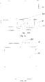
Figs. 1a and 1b are structural schematic view of an embodiment of a display panel; -
FIG. 2 is a structural schematic view of an embodiment of a display pixel circuit in a first area and a second area of the display panel of the present application; -
FIG. 3 is a structural schematic view of an embodiment of a virtual pixel circuit in the second area of the present application; -
FIG. 4a is a voltage simulation view of the first node of the first area and the second area of the display panel in the reset stage of a prior art; -
FIG. 4b is a voltage simulation view of the first node of the first area and the second area of the display panel in the reset stage of the present disclosure; -
FIG. 5 is a structural schematic view of an embodiment of the display device of the present application. - Currently, in a display device with full-screen, in order to realize the functions of selfie, visual call and fingerprint identification, a special-shaped area is usually set on the front of the display device. The special-shaped area is configured to install a camera, earpiece, fingerprint identification, or physical keys. However, by setting the special-shaped area on the display device, the load or number of pixels in the same row corresponding to the special-shaped area maybe changed, and the reset voltage of the pixel circuit of the display area located in the same row with the special-shaped area and connected to the same reference signal line in the reset stage maybe affected, the voltage difference at the node of the light-emitting device (i.e. the anode of the light-emitting device) is caused to be greater after the pixel circuit of the special-shaped area and other areas is reset, a greater difference in the rise time of the anode voltage of the light-emitting device maybe resulted, and a greater difference between the light-emitting time of the pixels in the special-shaped area and the light-emitting time of the pixels in the other areas within a frame maybe resulted. Thus, the display area corresponding to the special-shaped area and the other display areas are uneven, which resulting in an abnormal display.
- Specifically, the display panel with special-shaped area is a hole-punching screen or a screen with bangs. As shown in
FIG. 1a , taking the double hole-punching screen as an example, the special-shaped area 201 is set in the display area of the display panel. The special-shaped area 201 includes at least two hole-punching areas 122. The hole-punching areas 122 are isolated by theisolation area 123, so the pixels in the position of the hole-punching area 122 are lost. Moreover, since theisolation area 123 is not configured to display, theisolation area 123 has no the light-emitting device . As shown inFIG. 1b , taking the screen with bangs as an example, a special-shaped area 201 is set in the display area. The special-shaped area 201 is configured to install cameras and other devices. The existence of the special-shaped area 201 makes some pixels being lost in the display area. - Generally, the pixels in the pixel rows in different area receive the same reference signal, and the pixel driving circuit of the pixels in the same row is connected to the same reference signal line, so that the anode of the light-emitting device in the pixel driving circuit in the same row can be reset in the reset phase. However, since the lack of pixels in the pixel rows in the special-
shaped region 201, after the reset phase is completed, the anode voltage of the light-emitting device of the display pixel of the special-shaped area 201 may be different from the anode voltage of the light-emitting device in the display pixel of the normal display area, so that a greater difference in the anode voltage rise time of the light-emitting device is caused, and a greater difference in the light-emitting time of the pixels in the special-shaped area and the other areas within a frame maybe resulted, and a uneven pixel display in the display stage maybe resulted. - In order to overcome the above problems, achieve the purpose of eliminating display differences, and improve display effect in the present application, the present application provides a new technical solution. Technical solutions of the present application will be illustrated clearly and comprehensively by referring to the drawings of embodiments of the display panel and display.
- A display panel is provided in the present application. As shown in
FIG. 1a and 1b , the display panel includes afirst area 11 and asecond area 12. Thefirst area 11 includes a plurality of first pixel rows, thesecond area 12 includes a plurality of second pixel rows, and each of the first pixel row and the second pixel row includes a plurality of pixels. Specifically, since the special-shaped area 201 is set in thesecond area 12, some pixels in thesecond area 12 is lost. Specifically, the number of pixels in each second pixel row in thesecond area 12 is less than that in each first pixel row in thesecond area 11. Furthermore, the plurality of pixels located in the first pixel row are a plurality of display pixels, and the plurality of pixels located in the second pixel row are a plurality of display pixels and a plurality of virtual pixels. Moreover, the display pixel includes a display pixel circuit, the virtual pixel includes a virtual pixel circuit, and the virtual pixel circuit includes a compensation unit. The virtual pixel circuit is configured to reset compensation when the display pixel circuits which are located in the same of the second pixel row are. Thus, after the display pixel circuits in the first area and the second area are reset, the voltage difference at the nodes of the light-emitting devices (i.e. the anode of the light-emitting device) of the display pixel circuits is reduced, the difference of the light-emitting between thefirst area 11 and thesecond area 12 is reduced, and the display effect is improved. - Specifically, in one embodiment, the virtual pixel circuit and the reset unit of the display pixel circuit located in the same second pixel row in the
second area 12 are connected to the same reference signal line. The virtual pixels exist in each second pixel row of thesecond area 12, and the number of the pixels in the second pixel row in thesecond area 12 is less than the number of the pixels in the first pixel row in the first area. Thus, in the reset stage, the reset voltage is configured to reset the display pixel circuits of different numbers, so that the voltage of the anode of the light-emitting device of the display pixel circuit in thefirst area 11 and the voltage of the anode of the light-emitting device of the display pixel circuit in thesecond area 12 may be different, which resulting in a display difference in the display stage. Generally, in order to make the reset voltage being consistent, in the prior art a plurality of reference signal lines are used. Namely, the second pixel row located in thesecond area 12 and the first pixel row located in thefirst area 11 are connected to different reference signal lines, so that the reset voltage of the pixel circuit at thesecond area 12 and the reset voltage of the pixel circuit thefirst area 11 are the same, and different area of the display panel has the same display effect. However, the circuit is complex and the display effect is poor. In the present application, since the pixels of the first pixel row located in thefirst area 11 and the second pixel row located in thesecond area 12 receive the same reference signal, and the virtual pixel circuit located in the same second pixel row and the reset unit of the display pixel circuit are connected to the same reference signal line, not only the circuit of the display panel is simplified, but also in the reset stage, the compensation unit of the virtual pixel circuit can compensate the load of the display pixel circuit of thesecond area 12. Thus, the voltage of the anode of the light-emitting devices of the display pixel circuit of thefirst area 11 and the voltage of the display pixel circuit of thesecond area 12 are almost the same, the display of both thefirst area 11 and thesecond area 12 is uniform, and the display effect is improved. - In one embodiment, if the display panel is a double hole-punching screen as described in
FIG. 1a , the virtual pixel circuit is set at theisolation area 123. If the display panel is a screen with bangs as shown inFIG. 1b , the virtual pixel circuit can be set at the edge of the special-shapedarea 201, or the virtual pixel circuit can be set at the frame area of the display panel, as long as the purpose of compensating the display pixel circuit of thesecond area 12 is achieved, it will not be repeated below. - In an embodiment, as shown in
FIG. 2 andFIG. 3 ,FIG. 2 is a structural schematic view of an embodiment of a display pixel circuit in a first area and a second area of the display panel of the present application; andFIG. 3 is a structural schematic view of an embodiment of a virtual pixel circuit in the second area of the present application. Both the display pixel circuit and the virtual pixel circuit include: a writingunit 402, adriving unit 403, acontrol unit 404, and areset unit 405. Thewriting unit 402 is configured to receive the first scanning signal S1 and be driven by the first scanning signal S1 to write the data signal to the driving node n2 in the writing stage. The drivingunit 403 is configured to connect to thewriting unit 402 by driving the node n2. Thecontrol unit 404 is configured to receive the enable signal EM and connect thedriving unit 403, so that the drivingunit 403 is connected to the power signal line by thecontrol unit 404. Thereset unit 405 is configured to receive a second scan signal, connect the driving node n2 and thecontrol unit 404, to be driven by the second scan signal to receive the reference signal Verf, and thereset unit 405 further resets the driving node n2 and the first node n1 which is between thereset unit 405 and thecontrol unit 404 by using the reference signal Verf. - As shown in the structural schematic view of the display pixel circuit shown in
FIG. 2 , the first node n1 of thecontrol unit 404 and thereset unit 405 of the display pixel circuit is connected to the light-emittingdevice 401. As shown in the structural schematic view of the display pixel circuit shown inFIG. 3 , the driving node n2 of thedriving unit 403 in the virtual pixel circuit is connected to acompensation unit 406, and the first node n1 of thecontrol unit 404 and thereset unit 405 in the virtual pixel circuit is not connected to the light-emittingdevice 401. - In one embodiment, both the display pixels of the first pixel row and the display pixels of the second pixel row are configured to display in the display stage. Therefore, both the display pixels of the first pixel row and the display pixels of the second pixel row have light-emitting devices. Since the virtual pixels are not configured to display in the display stage, the virtual pixels could not include light-emitting devices. The light-emitting
device 401 can be an organic light emitting diode OLED, which may includes a red OLED, a blue OLED, and a green OLED. In another embodiment, the light-emittingdevice 401 may also includes a white OLED. There is not limited here, which is mainly configured to display on the display panel, as long as the display effect required by the display panel can be achieved. - In one embodiment, the
compensation unit 406 is a compensation capacitor or a compensation resistor. Specifically, as shown inFIG. 3 , thecompensation unit 406 in the virtual pixel circuit is a compensation capacitor, one end of thecompensation unit 406 is connected to the driving node n2, and the other end of thecompensation unit 406 is connected to the power signal line and configured to receive the power signal VDD. In another embodiment, thecompensation unit 406 of the virtual pixel circuit can also be a compensation resistor, which can also be a compensation capacitor as shown inFIG. 3 . One end of thecompensation unit 406 is connected to the driving node n2, and the other end of thecompensation unit 406 is connected to the power signal line and configured to receive the power signal VDD. As long as thecompensation unit 406 can play a compensation role in the reset stage, so that the voltage of the first node n1 (anode of the light-emitting device) of the display pixel circuit of thesecond area 12 and the voltage of the display pixel circuit of thefirst area 11 are almost the same, it will not be repeated below. - In one embodiment, the driving node n2 of each of the virtual pixel circuit is connected to one compensation capacitor. In another embodiment, in order to make the voltage of the first node n1 (anode of the light-emitting device) of the display pixel circuit of the
second area 12 and the voltage of the display pixel circuit of thesecond area 12 being almost the same after the reset phase is completed, the compensation capacitor can also be connected to the driving node n2 of the virtual pixel circuit. Namely, the number of the compensation capacitors is less than or equal to the number of the virtual pixels. Specifically, in one embodiment, the number of the compensation capacitors is the difference between the number of the virtual pixels in the first pixel row and the number of the virtual pixels the second pixel row. For example, in the screen with bangs, 200 pixels are lost in the position of the special-shapedarea 201, and the special-shaped area includes 5 the second pixel rows, and 40 pixels are lost in each second pixel row, then 40 virtual pixel circuits with the compensation capacitor can be set in each second pixel row and connected to the reference signal line of each row. - As shown in
FIG. 1a , in order to ensure the narrow frame design, thesecond area 12 may include a virtual pixel area, the virtual pixel area includes two hole-punchingareas 122 and anisolation area 123 located between the two hole-punchingareas 122, and the virtual pixels are located in theisolation area 123. - In another embodiment, the display panel is as shown in
FIG. 1b , the virtual pixel can be set at the edge of the special-shapedarea 201, and the virtual pixel can also be set at the frame area of the display panel. - There are many specific setting manners of the display pixel circuit and the virtual pixel circuit in the present application. In the embodiment, the 7T1C circuit is used as an example for the display pixel circuit and the virtual pixel circuit. Specifically, in a 7T1C circuit, the
writing unit 402 includes a first transistor M1, and a second transistor M2. The first transistor M1 includes a first pathway terminal, a second pathway terminal, and a control terminal. Furthermore, the first pathway terminal of the first transistor M1 is connected to a data signal line and configured to receive the data signal. The second pathway terminal of the first transistor M1 is connected to both thedriving unit 403 and thecontrol unit 404. Specifically, the second pathway terminal of the first transistor M1 is connected to the first pathway terminal of a third transistor M3 of thedriving unit 403 and the second pathway terminal of a sixth transistor M6 of thecontrol unit 404. The control terminal of the first transistor M1 is connected to the first scanning signal line and configured to receive a first scanning signal S1. The second transistor M2 includes a first pathway terminal, a second pathway terminal, and a control terminal. Furthermore, the first pathway terminal of the second transistor M2 is connected to thedriving unit 403. Specifically, the first pathway terminal of the second transistor M2 is connected to the control terminal of the third transistor M3 of the driving unit 403 (i.e. the driving node n2). The second pathway terminal of the second transistor M2 is connected to the second pathway terminal of the third transistor M3 of thedriving unit 403 and the first pathway terminal of a seventh transistor M7 of thecontrol unit 404. The control terminal of the second transistor M2 is connected to the first scanning signal line and configured to receive the first scanning signal S1. - The driving
unit 403 includes a third transistor M3. The third transistor M3 includes a first pathway terminal, a second pathway terminal and a control terminal, furthermore, the first pathway terminal of the third transistor M3 is connected to thecontrol unit 404 and thewriting unit 402. Specifically, the first pathway terminal of the third transistor M3 is connected to the second pathway terminal of the sixth transistor M6 of thecontrol unit 404, and the second pathway terminal of the first transistor M1 of thewriting unit 402. The second pathway terminal of the third transistor M3 is connected to thecontrol unit 404 and thewriting unit 402. Specifically, the second pathway terminal of the third transistor M3 is connected to the first pathway terminal of a seventh transistor M7 of thecontrol unit 404, and the second pathway terminal of the second transistor m2 of thewriting unit 402, the control terminal of the third transistor M3 is connected to thereset unit 405 and thewriting unit 402. Specifically, the control terminal of the third transistor M3 is connected to the first pathway terminal of the fourth transistor M4 of thereset unit 405 and the first pathway terminal of the second transistor m2 of thewriting unit 402. - In the embodiment, the
reset unit 405 is configured to receive the second scanning signal, and thereset unit 405 is connected to the driving node n2 of thedriving unit 403 and thecontrol unit 404, and thereset unit 405 receives the reference signal Verf when driven by the second scanning signal, and thereset unit 405 resets the driving node n2 and the first node n1 which is between thereset unit 405 and thecontrol unit 404 according to the reference signal Verf. In one embodiment, the second scan signal includes a first scanning reset sub-signal S2 and a second scanning reset sub-signal S3. Thereset unit 405 includes a first reset sub-unit and a second reset sub-unit. The first reset sub-unit is configured to receive the first scanning reset sub-signal S2 and the reference signal Verf, and the first reset sub-unit connects the driving node n2, and the first reset sub-unit resets the driving node n2 by using the reference signal Verf during the first reset sub-period corresponding to the first scanning reset sub-signal S2. The second reset sub-unit is configured to receive the second scanning reset sub-signal S3 and the reference signal Verf, and the second reset sub-unit connects the first node n1, and the second reset sub-unit resets the first node n1 by using the reference signal Verf during the second reset sub-period corresponding to the second scanning reset sub-signal S3. - The first reset sub-unit includes a fourth transistor M4.The fourth transistor M4 includes a first pathway terminal, a second pathway terminal and, a control terminal. Furthermore, the first pathway terminal of the fourth transistor M4 is connected to the
driving unit 403. Specifically, the first pathway terminal of the fourth transistor M4 is connected to the control terminal of the third transistor M3 of the driving unit 403 (i.e. the driving node n2). The second pathway terminal of the fourth transistor M4 is connected to the reference signal line and configured to receive the reference signal Verf. The control terminal of the fourth transistor M4 is connected to a first scanning reset sub-signal line and configured to receive the first scanning reset sub-signal S2. - In one embodiment, the second reset sub-unit includes a fifth transistor M5. The fifth transistor M5 includes a first pathway terminal, a second pathway terminal, and a control terminal. Furthermore, the first pathway terminal of the fifth transistor M5 is connected to the first node n1. Specifically, the first pathway terminal of the fifth transistor M5 is connected to the second pathway terminal of a seventh transistor M7 of the
control unit 404. In the display pixel, the first pathway terminal of the fifth transistor M5 is also connected to the anode of the light-emittingdevice 401. The second pathway terminal of the fifth transistor M5 is connected to the reference signal line and configured to receive the reference signal Verf, and the control terminal of the fifth transistor M5 is connected to a second scanning reset sub-signal line and configured to receive a second scanning reset sub-signal S3. - The
control unit 404 includes a sixth transistor M6 and a seventh transistor M7. The sixth transistor M6 includes a first pathway terminal, a second pathway terminal and a control terminal, furthermore, the first pathway terminal of the sixth transistor M6 is connected to the power signal line and configured to receive the power signal VDD, the second pathway terminal of the sixth transistor M6 is connected to thedriving unit 403. Specifically, the second pathway terminal of the sixth transistor M6 is connected to the first pathway terminal of the third transistor M3 of thedriving unit 403, the control terminal of the sixth transistor M6 is connected to an enable signal line and configured to receive the enable signal EM. The seventh transistor M7 includes a first pathway terminal, a second pathway terminal, and a control terminal. Furthermore, the first pathway terminal of the seventh transistor M7 is connected to the second pathway terminal of the sixth transistor M6, the second pathway terminal of the seventh transistor M7 is connected to the first node n1, and the control terminal of the seventh transistor M7 is connected to the enable signal line and configured to receive the enable signal EM. - In one embodiment, the display pixel circuit and the virtual pixel circuit also include a storage capacitor Cst, the storage capacitor Cst includes a first pathway terminal and a second pathway terminal, the first pathway terminal of the storage capacitor Cst is connected to the power signal line, and the second pathway terminal of the storage capacitor Cst is connected to the control terminal of the third transistor M3.
- In the reset phase, both the fourth transistor M4 and the fifth transistor M5 in the
reset unit 405 are turned on, and the driving node n2 of thedriving unit 403 and the anode of the light-emitting device 401 (i.e., the first node n1) are reset by the reference signal Verf. In the display panel of prior art, since the number of pixels in each row of the second pixel row of thesecond area 12 is less than that in each row of the first pixel row of thefirst area 11, the first pixel row and the second pixel row receive the same reference signal. After the reset is completed, the voltage of the anode of the light-emitting device of the display pixel circuit of the first pixel row of thefirst area 11 is different from the voltage of the anode of the light-emitting device of the display pixel circuit of the second pixel row of thesecond area 12. Furthermore, the display of thefirst area 11 and thesecond area 12 may be uneven, and the display effect will be poor, in the writing stage and the light-emitting stage. In the display panel of the present application, the virtual pixels are disposed in each second pixel row, the second pixels and the virtual pixels are connected to the same reference line, and the driving unit of the virtual pixel circuit is connected to the compensation unit at the driving node n2. When resetting in the reset stage, the compensation unit compensates the pixels of one of the second pixel rows, to make the anode of the light-emitting devices of the display pixel circuits of thefirst area 11 and thesecond area 12 have almost the same electric potential, so that the voltage difference between the anodes of the light-emitting devices corresponding to the display pixel circuits of thefirst area 11 and thesecond area 12 is reduced, and the display of thefirst area 11 and thesecond area 12 is uniform, the display effect is improved. - The embodiment takes 7T1C circuit as an example. In other embodiments, the mode of the embodiment can also be applied to, for example, 6tlc circuit, 3tlc circuit, or 8tlc circuit, which is not limited here. As long as the anode voltage of the light-emitting devices in the first area and the second area have almost the same electric potential after the reset phase is completed.
- Referring to
FIG. 4a, FIG. 4a is a voltage simulation view of the first node of the first area and the second area of the display panel in the reset stage of the prior art. Furthermore, the anode voltage of the light-emitting device (i.e., the first node n1) of the display pixel circuit of thesecond area 12 is -2.6457V after the reset phase is completed, and the anode voltage of the light-emitting device (i.e., the first node n1) of the display pixel circuit of thefirst area 11 is -2.6056V after the reset phase is completed. It can be seen that in the display panel of prior art, after the reset phase is completed, the difference between the anode voltage of the light-emitting device of the display pixel circuit of the first area and the second area is 40.1mV. - Referring to
FIG. 4b, FIG. 4b is a voltage simulation view of the first node of the first area and the second area of the display panel in the reset stage of the present application. Furthermore, under the compensation of the compensation unit of the virtual pixel circuit, the anode voltage of the light-emitting device of the display pixel circuit of the second area is - 2.5997V after the reset phase is completed, and the anode voltage of the light-emitting device of the display pixel circuit of the first area is -2.5999V after the reset phase is completed. It can be seen that the display panel of the present application, after the reset phase is completed, the difference between the anode voltage of the light-emitting device of the display pixel circuit of the first area and the second area is 0.2mV. Compared with the prior art, the technical solution of the present application is significantly reduced the anode voltage of the light-emitting device after the reset phase of the display pixels of the first area and the second area is completed. Furthermore, the difference between the anode voltage of the light-emitting device of the display pixel circuit of the first area and the second area of the present application is 0.2mV, which is caused by the accuracy of the simulator. Theoretically, under the compensation of the compensation unit, the anode voltage of the light-emitting device of the display pixel circuit of the first area and the second area is the same after the reset stage is completed by the technical solution of the present application. - The display panel provided by the present application can be a double-sided display panel, a flexible display panel, or a full-screen display panel. The flexible display panel can be applied to a curved electronic device, the double-sided display panel can be applied to the panel which enables the personnel on both sides of the display panel to see the display content, the full-screen display panel can be applied to full-screen mobile phones or other devices, which is not limited here.
- In the display panel provided by the present application, by setting a virtual pixel with the virtual pixel circuit in the second pixel row of the second area, the virtual pixel circuit further includes the compensation unit, and the compensation unit is connected to the driving node and the power signal line to compensate the anode voltage of the light-emitting device of the display pixel circuit of the second area in the reset stage. So that the anode voltage of the light-emitting device of the display pixel circuit of the second area have almost the same electric potential with the anode voltage of the light-emitting device of the display pixel circuit of the first area, so as to the display difference between the first area and the second area in the display stage is reduced and the display effect is improved.
- Referring to
FIG. 5, FIG. 5 is a structural schematic view of an embodiment of the display device of the present application. The display device includes the display panel described above. - In one embodiment, the display device can be any product or component with display function, such as mobile phone, tablet computer, television, display, notebook computer, digital photo frame, navigator, etc. Other essential components of the display panel should be understood by those skilled in the art, and that will not be repeated below, nor should it be regarded as a limitation of the present application. The embodiment of the display device can refer to the embodiment of the above display panel, and the repetition will not be repeated.
- In each embodiment of the present application, the display panel and display device only describe some related structures, and other structures are the same as those of the display panel and display device in the prior art, which will not be repeated here.
- The above description only shows some embodiments of the present disclosure, but does not limit the scope of the present disclosure. Any equivalent structural or process transformation performed based on the drawings and the specification of the present disclosure, directly or indirectly applied in any other related arts, should be within the scope of the present disclosure.
Claims (17)
- A display panel, comprising:a first area and a second area, the first area comprises a plurality of first pixel rows, the second area comprises a plurality of second pixel rows, and each of the first pixel row and the second pixel row comprise a plurality of pixels, the number of the pixels of each first pixel row is greater than the number of the pixels of each second pixel row; wherein the plurality of pixels of the first pixel row are a plurality of display pixels, and the plurality of the pixels of the second pixel row are a plurality of display pixels and a plurality of virtual pixels;each of the plurality of display pixels comprises a display pixel circuit, each of the plurality of virtual pixels comprises a virtual pixel circuit, the virtual pixel circuit comprises a compensation unit, and the virtual pixel circuit is configured to compensate the display pixel circuits of one of the plurality of second pixel rows when the display pixel circuits of the one of the plurality of second pixel rows are reset; so that, after the display pixel circuits in both the first area and the second area are reset, a voltage difference of nodes of light-emitting devices corresponding to the display pixel circuits is reduced.
- The display panel of claim 1, wherein
each of the display pixel circuit and the virtual pixel circuit comprises:a writing unit, configured to receive a first scanning signal, and be driven by the first scanning signal to write a data signal to a driving node in a writing stage;a driving unit, connected to the writing unit by a driving node;a control unit, configured to receive an enable signal, wherein the control unit is connected to the driving unit, so that the driving unit is connected to a power signal line by the control unit;a reset unit, configured to receive a second scan signal, wherein the control unit is connected the driving node and the control unit, the reset unit is driven by the second scan signal to receive a reference signal, and the reset unit resets the driving node and a first node which is between the reset unit and the control unit according to the reference signal;wherein, the first node of the control unit of the display pixel circuit is connected to a light-emitting device, and the driving node of the virtual pixel circuit is connected to the compensation unit. - The display panel of claim 2, whereinthe pixels of both the plurality of first pixel rows and the plurality of second pixel rows receive a same reference signal, and the reset units of the display pixel circuits of and the reset units of the virtual pixel circuits which are disposed in one of the plurality of second pixel rows are connected to the same reference signal line;the compensation unit is a compensation capacitor or a compensation resistor.
- The display panel of claim 3, wherein
the virtual pixel circuit does not comprise a light-emitting device. - The display panel of claim 2, wherein
the compensation unit is a compensation capacitor or a compensation resistor. - The display panel of claim 5, wherein
the compensation unit is the compensation capacitor, one end of the compensation unit is connected to the driving node, and the other end the compensation unit is connected to the power signal line. - The display panel of claim 6, wherein
the number of compensation capacitors is less than or equal to the number of the virtual pixels. - The display panel of claim 6, wherein
the number of compensation capacitors is equal to a difference between the number of the pixels of the first pixel row and the number of the pixels of the second pixel row. - The display panel of claim 1, wherein the second area comprises:
a virtual pixel area, where the virtual pixel area comprises two hole-punching areas and an isolation area between the two hole-punching areas, and the plurality of virtual pixel is located in the isolation area. - The display panel of claim 2, wherein the writing unit comprises:a first transistor, comprising a first pathway terminal, a second pathway terminal, and a control terminal; wherein, the first pathway terminal of the first transistor is connected to the data signal line and configured to receive the data signal, the second pathway terminal of the first transistor is connected to the driving unit and the control unit, and the control terminal of the first transistor is connected to a first scanning signal line and configured to receive the first scanning signal;a second transistor, comprising a first pathway terminal, a second pathway terminal, and a control terminal; wherein, the first pathway terminal of the second transistor is connected to the driving unit, the second pathway terminal of the second transistor is connected to the driving unit and the control unit, and the control terminal of the second transistor is connected to the first scanning signal line and configured to receive the first scanning signal.
- The display panel of claim 2, wherein the driving unit comprises:
a third transistor, comprising a first pathway terminal, a second pathway terminal, and a control terminal; wherein, the first pathway terminal of the third transistor is connected to the control unit and the writing unit, and the second pathway terminal of the third transistor is connected to the control unit and the writing unit, the control terminal of the third transistor is connected to the reset unit and the writing unit. - The display panel of claim 2, wherein the reset unit comprises:a first reset sub-unit, configured to receive a first scanning reset sub-signal and the reference signal; wherein the first reset sub-unit is connected to the driving node, and reset the driving node by using the reference signal during a first reset sub-period corresponding to the first scanning reset sub-signal;a second reset sub-unit, configured to receive a second scanning reset sub-signal and the reference signal; wherein the second reset sub-unit is connected to the first node, and the first reset sub-unit resets the first node by using the reference signal during a second reset sub-period corresponding to the second scanning reset sub-signal.
- The display panel of claim 12, wherein the first reset sub-unit comprises:
a fourth transistor, comprising a first pathway terminal, a second pathway terminal and a control terminal; wherein, the first pathway terminal of the fourth transistor is connected to the driving node, the second pathway terminal of the fourth transistor is connected to a reference signal line and configured to receive the reference signal, and the control terminal of the fourth transistor is connected to the first scanning reset sub-signal line and configured to receive the first scanning reset sub-signal. - The display panel of claim 12, wherein the second reset sub-unit comprises:
a fifth transistor, comprising a first pathway terminal, a second pathway terminal and a control terminal; wherein, the first pathway terminal of the fifth transistor is connected to the first node, the second pathway terminal of the fifth transistor is connected to the reference signal line and configured to receive the reference signal, and the control terminal of the fifth transistor is connected to a second scanning reset sub-signal line to receive the second scanning reset sub-signal. - The display panel of claim 2, wherein the control unit comprises:a sixth transistor, comprising a first pathway terminal, a second pathway terminal, and a control terminal; wherein, the first pathway terminal of the sixth transistor is connected to the power signal line and configured to receive the power signal, the second pathway terminal of the sixth transistor is connected to the driving unit, and the control terminal of the sixth transistor is connected to an enable signal line and configured to receive the enable signal;a seventh transistor, comprising a first pathway terminal, a second pathway terminal, and a control terminal; wherein, the first pathway terminal of the seventh transistor is connected to the second pathway terminal of the sixth transistor, the second pathway terminal of the seventh transistor is connected to the first node, and the control terminal of the seventh transistor is connected to the enable signal line and configured to receive the enable signal.
- The display panel of claim 2, wherein each of the display pixel circuit and the virtual pixel circuit further comprises:
a storage capacitor, comprising a first pathway terminal and a second pathway terminal; wherein, the first pathway terminal of the storage capacitor is connected to the power signal line, and the second pathway terminal of the storage capacitor is connected to the driving unit. - A display device, comprising
a display panel, the display panel is the display panel according to any one of claims 1 to 16.
Applications Claiming Priority (2)
| Application Number | Priority Date | Filing Date | Title |
|---|---|---|---|
| CN202010308108.2A CN111599282B (en) | 2020-04-17 | 2020-04-17 | Display panel and display device |
| PCT/CN2021/083388 WO2021208708A1 (en) | 2020-04-17 | 2021-03-26 | Display panel and display device |
Publications (2)
| Publication Number | Publication Date |
|---|---|
| EP4044161A1 true EP4044161A1 (en) | 2022-08-17 |
| EP4044161A4 EP4044161A4 (en) | 2022-10-12 |
Family
ID=72183412
Family Applications (1)
| Application Number | Title | Priority Date | Filing Date |
|---|---|---|---|
| EP21787846.1A Pending EP4044161A4 (en) | 2020-04-17 | 2021-03-26 | DISPLAY PANEL AND DISPLAY DEVICE |
Country Status (6)
| Country | Link |
|---|---|
| US (1) | US11769444B2 (en) |
| EP (1) | EP4044161A4 (en) |
| JP (1) | JP7378618B2 (en) |
| KR (1) | KR102631196B1 (en) |
| CN (1) | CN111599282B (en) |
| WO (1) | WO2021208708A1 (en) |
Families Citing this family (7)
| Publication number | Priority date | Publication date | Assignee | Title |
|---|---|---|---|---|
| CN111599282B (en) | 2020-04-17 | 2021-12-14 | 昆山国显光电有限公司 | Display panel and display device |
| WO2022099610A1 (en) * | 2020-11-13 | 2022-05-19 | 京东方科技集团股份有限公司 | Display substrate, display panel, and display apparatus |
| CN112562522A (en) * | 2020-12-14 | 2021-03-26 | 昆山国显光电有限公司 | Display panel and display device |
| CN113096588B (en) * | 2021-04-07 | 2022-08-23 | 京东方科技集团股份有限公司 | Auxiliary pixel circuit, display panel and display device |
| CN113409727B (en) * | 2021-05-19 | 2023-01-31 | Oppo广东移动通信有限公司 | Pixel driving circuit, display panel, control method of display panel and display device |
| US12266302B2 (en) | 2021-08-27 | 2025-04-01 | Chengdu Boe Optoelectronics Technology Co., Ltd. | Pixel circuit, driving method therefor, and display apparatus |
| CN113851493B (en) * | 2021-10-29 | 2025-06-03 | 京东方科技集团股份有限公司 | Display substrate, display panel and display device |
Family Cites Families (22)
| Publication number | Priority date | Publication date | Assignee | Title |
|---|---|---|---|---|
| KR102152950B1 (en) * | 2014-04-09 | 2020-09-08 | 삼성디스플레이 주식회사 | Organic light emitting display |
| KR102285390B1 (en) * | 2015-01-28 | 2021-08-04 | 삼성디스플레이 주식회사 | Organic light emitting display apparatus |
| US10490122B2 (en) * | 2016-02-29 | 2019-11-26 | Samsung Display Co., Ltd. | Display device |
| SG11201807505SA (en) * | 2016-03-28 | 2018-09-27 | Apple Inc | Light-emitting diode displays |
| KR102611958B1 (en) * | 2016-09-23 | 2023-12-12 | 삼성디스플레이 주식회사 | Display device |
| CN106843389B (en) * | 2017-01-09 | 2022-08-05 | Oppo广东移动通信有限公司 | Electronic device |
| CN107633807B (en) * | 2017-09-08 | 2019-10-15 | 上海天马有机发光显示技术有限公司 | A display panel and display device |
| CN107481669A (en) * | 2017-09-08 | 2017-12-15 | 武汉天马微电子有限公司 | A display panel and a display device |
| JP6872795B2 (en) * | 2017-10-05 | 2021-05-19 | 株式会社Joled | Display device |
| CN107994060B (en) * | 2017-11-28 | 2021-07-20 | 武汉天马微电子有限公司 | An organic light-emitting display panel and display device |
| CN107993579B (en) * | 2017-11-29 | 2019-11-12 | 武汉天马微电子有限公司 | Display panel, driving method thereof and display device |
| CN108010947B (en) * | 2017-11-29 | 2021-01-08 | 上海天马有机发光显示技术有限公司 | Organic light-emitting display panel and organic light-emitting display device |
| CN108550609B (en) | 2018-05-14 | 2021-02-12 | 昆山国显光电有限公司 | Display panel, manufacturing method thereof and display device |
| US11263968B2 (en) * | 2018-06-20 | 2022-03-01 | Boe Technology Group Co., Ltd. | Display substrate and driving method thereof, and display device |
| CN108828861B (en) * | 2018-07-27 | 2021-05-04 | 厦门天马微电子有限公司 | Array substrate and display device |
| KR102705173B1 (en) * | 2018-11-30 | 2024-09-12 | 삼성디스플레이 주식회사 | Display panel and electronic device having the same |
| CN110111742B (en) * | 2019-04-22 | 2020-09-01 | 武汉华星光电半导体显示技术有限公司 | Pixel circuit of organic light-emitting device and organic light-emitting display panel |
| KR102907359B1 (en) * | 2019-05-31 | 2026-01-02 | 삼성디스플레이 주식회사 | Display panel |
| CN110444120B (en) * | 2019-08-19 | 2021-10-12 | 京东方科技集团股份有限公司 | Display panel and driving method thereof |
| CN110649080B (en) * | 2019-09-30 | 2021-10-15 | 武汉天马微电子有限公司 | A display panel and display device |
| CN111599282B (en) * | 2020-04-17 | 2021-12-14 | 昆山国显光电有限公司 | Display panel and display device |
| CN112562522A (en) * | 2020-12-14 | 2021-03-26 | 昆山国显光电有限公司 | Display panel and display device |
-
2020
- 2020-04-17 CN CN202010308108.2A patent/CN111599282B/en active Active
-
2021
- 2021-03-26 JP JP2022528192A patent/JP7378618B2/en active Active
- 2021-03-26 KR KR1020227014556A patent/KR102631196B1/en active Active
- 2021-03-26 WO PCT/CN2021/083388 patent/WO2021208708A1/en not_active Ceased
- 2021-03-26 EP EP21787846.1A patent/EP4044161A4/en active Pending
-
2022
- 2022-03-09 US US17/690,373 patent/US11769444B2/en active Active
Also Published As
| Publication number | Publication date |
|---|---|
| US20220199004A1 (en) | 2022-06-23 |
| CN111599282B (en) | 2021-12-14 |
| US11769444B2 (en) | 2023-09-26 |
| JP2023501703A (en) | 2023-01-18 |
| EP4044161A4 (en) | 2022-10-12 |
| CN111599282A (en) | 2020-08-28 |
| KR20220065073A (en) | 2022-05-19 |
| KR102631196B1 (en) | 2024-01-31 |
| WO2021208708A1 (en) | 2021-10-21 |
| JP7378618B2 (en) | 2023-11-13 |
Similar Documents
| Publication | Publication Date | Title |
|---|---|---|
| US11769444B2 (en) | Display panel and display device with virtual pixel circuit | |
| US12260799B2 (en) | Pixel circuit, driving method thereof and display device | |
| US11462592B2 (en) | Array substrate with pixel circuits sharing voltage control circuit, driving method, organic light emitting display panel and display device | |
| US10923037B2 (en) | Gate driving circuit, method for implementing gate driving circuit, and method for driving gate driving circuit | |
| US11657756B2 (en) | Display panel and display apparatus | |
| CN210837108U (en) | Display panel and display device | |
| CN108010951A (en) | An organic light emitting display panel and a display device | |
| CN113707090A (en) | Driving method of pixel driving circuit, display panel and display device | |
| WO2017041290A1 (en) | Array substrate for capacitive in-cell touch panel and method for driving the same, related display panels, and related display apparatus | |
| US20170083163A1 (en) | Touch display circuit and driving method thereof, display apparatus | |
| US11393425B2 (en) | Pixel circuit, display module and driving method thereof | |
| US10971091B2 (en) | Array substrate, display panel and driving method thereof, and display device | |
| CN113160744B (en) | Display panel, driving method thereof, and display device | |
| CN114783372B (en) | Pixel driving circuit, display panel and display device | |
| CN110867162A (en) | Pixel driving circuit, driving method thereof and display panel | |
| CN113920946A (en) | Gate driver, driving method thereof and display device | |
| US11244630B2 (en) | Shift register unit, gate driving circuit, display device, and method for controlling shift register unit | |
| CN105679279A (en) | Self-refreshing display driving device, driving method and display device | |
| CN112562522A (en) | Display panel and display device | |
| CN112489584A (en) | Display panel and display device | |
| CN111312170A (en) | Pixel driving circuit and display device | |
| CN118737011B (en) | Scan driving circuit, gate driving circuit and display panel | |
| CN104700781B (en) | Pixel circuit, driving method thereof and display device | |
| CN116312405B (en) | Pixel driving circuit and driving method thereof, and display device | |
| US10573670B2 (en) | Array substrate, method for fabricating the same, display device and method for driving display device |
Legal Events
| Date | Code | Title | Description |
|---|---|---|---|
| STAA | Information on the status of an ep patent application or granted ep patent |
Free format text: STATUS: THE INTERNATIONAL PUBLICATION HAS BEEN MADE |
|
| PUAI | Public reference made under article 153(3) epc to a published international application that has entered the european phase |
Free format text: ORIGINAL CODE: 0009012 |
|
| STAA | Information on the status of an ep patent application or granted ep patent |
Free format text: STATUS: REQUEST FOR EXAMINATION WAS MADE |
|
| 17P | Request for examination filed |
Effective date: 20220502 |
|
| AK | Designated contracting states |
Kind code of ref document: A1 Designated state(s): AL AT BE BG CH CY CZ DE DK EE ES FI FR GB GR HR HU IE IS IT LI LT LU LV MC MK MT NL NO PL PT RO RS SE SI SK SM TR |
|
| REG | Reference to a national code |
Ref country code: DE Ref legal event code: R079 Free format text: PREVIOUS MAIN CLASS: G09F0009330000 Ipc: G09G0003320000 |
|
| A4 | Supplementary search report drawn up and despatched |
Effective date: 20220913 |
|
| RIC1 | Information provided on ipc code assigned before grant |
Ipc: G09G 3/30 20060101ALI20220907BHEP Ipc: G09F 9/33 20060101ALI20220907BHEP Ipc: G09G 3/32 20160101AFI20220907BHEP |
|
| DAV | Request for validation of the european patent (deleted) | ||
| DAX | Request for extension of the european patent (deleted) | ||
| STAA | Information on the status of an ep patent application or granted ep patent |
Free format text: STATUS: EXAMINATION IS IN PROGRESS |
|
| 17Q | First examination report despatched |
Effective date: 20240827 |