EP4043534A2 - Lumineszente folie und vorrichtung damit - Google Patents
Lumineszente folie und vorrichtung damit Download PDFInfo
- Publication number
- EP4043534A2 EP4043534A2 EP21218196.0A EP21218196A EP4043534A2 EP 4043534 A2 EP4043534 A2 EP 4043534A2 EP 21218196 A EP21218196 A EP 21218196A EP 4043534 A2 EP4043534 A2 EP 4043534A2
- Authority
- EP
- European Patent Office
- Prior art keywords
- equal
- light emitting
- less
- zinc
- layer
- Prior art date
- Legal status (The legal status is an assumption and is not a legal conclusion. Google has not performed a legal analysis and makes no representation as to the accuracy of the status listed.)
- Granted
Links
Images

Classifications
-
- C—CHEMISTRY; METALLURGY
- C09—DYES; PAINTS; POLISHES; NATURAL RESINS; ADHESIVES; COMPOSITIONS NOT OTHERWISE PROVIDED FOR; APPLICATIONS OF MATERIALS NOT OTHERWISE PROVIDED FOR
- C09K—MATERIALS FOR MISCELLANEOUS APPLICATIONS, NOT PROVIDED FOR ELSEWHERE
- C09K11/00—Luminescent materials, e.g. electroluminescent or chemiluminescent
- C09K11/08—Luminescent materials, e.g. electroluminescent or chemiluminescent containing inorganic luminescent materials
- C09K11/70—Luminescent materials, e.g. electroluminescent or chemiluminescent containing inorganic luminescent materials containing phosphorus
-
- C—CHEMISTRY; METALLURGY
- C09—DYES; PAINTS; POLISHES; NATURAL RESINS; ADHESIVES; COMPOSITIONS NOT OTHERWISE PROVIDED FOR; APPLICATIONS OF MATERIALS NOT OTHERWISE PROVIDED FOR
- C09K—MATERIALS FOR MISCELLANEOUS APPLICATIONS, NOT PROVIDED FOR ELSEWHERE
- C09K11/00—Luminescent materials, e.g. electroluminescent or chemiluminescent
- C09K11/02—Use of particular materials as binders, particle coatings or suspension media therefor
-
- B—PERFORMING OPERATIONS; TRANSPORTING
- B82—NANOTECHNOLOGY
- B82Y—SPECIFIC USES OR APPLICATIONS OF NANOSTRUCTURES; MEASUREMENT OR ANALYSIS OF NANOSTRUCTURES; MANUFACTURE OR TREATMENT OF NANOSTRUCTURES
- B82Y10/00—Nanotechnology for information processing, storage or transmission, e.g. quantum computing or single electron logic
-
- B—PERFORMING OPERATIONS; TRANSPORTING
- B82—NANOTECHNOLOGY
- B82Y—SPECIFIC USES OR APPLICATIONS OF NANOSTRUCTURES; MEASUREMENT OR ANALYSIS OF NANOSTRUCTURES; MANUFACTURE OR TREATMENT OF NANOSTRUCTURES
- B82Y20/00—Nanooptics, e.g. quantum optics or photonic crystals
-
- B—PERFORMING OPERATIONS; TRANSPORTING
- B82—NANOTECHNOLOGY
- B82Y—SPECIFIC USES OR APPLICATIONS OF NANOSTRUCTURES; MEASUREMENT OR ANALYSIS OF NANOSTRUCTURES; MANUFACTURE OR TREATMENT OF NANOSTRUCTURES
- B82Y30/00—Nanotechnology for materials or surface science, e.g. nanocomposites
-
- B—PERFORMING OPERATIONS; TRANSPORTING
- B82—NANOTECHNOLOGY
- B82Y—SPECIFIC USES OR APPLICATIONS OF NANOSTRUCTURES; MEASUREMENT OR ANALYSIS OF NANOSTRUCTURES; MANUFACTURE OR TREATMENT OF NANOSTRUCTURES
- B82Y40/00—Manufacture or treatment of nanostructures
-
- C—CHEMISTRY; METALLURGY
- C09—DYES; PAINTS; POLISHES; NATURAL RESINS; ADHESIVES; COMPOSITIONS NOT OTHERWISE PROVIDED FOR; APPLICATIONS OF MATERIALS NOT OTHERWISE PROVIDED FOR
- C09K—MATERIALS FOR MISCELLANEOUS APPLICATIONS, NOT PROVIDED FOR ELSEWHERE
- C09K11/00—Luminescent materials, e.g. electroluminescent or chemiluminescent
- C09K11/08—Luminescent materials, e.g. electroluminescent or chemiluminescent containing inorganic luminescent materials
- C09K11/88—Luminescent materials, e.g. electroluminescent or chemiluminescent containing inorganic luminescent materials containing selenium, tellurium or unspecified chalcogen elements
- C09K11/881—Chalcogenides
- C09K11/883—Chalcogenides with zinc or cadmium
-
- H—ELECTRICITY
- H05—ELECTRIC TECHNIQUES NOT OTHERWISE PROVIDED FOR
- H05B—ELECTRIC HEATING; ELECTRIC LIGHT SOURCES NOT OTHERWISE PROVIDED FOR; CIRCUIT ARRANGEMENTS FOR ELECTRIC LIGHT SOURCES, IN GENERAL
- H05B33/00—Electroluminescent light sources
- H05B33/12—Light sources with substantially two-dimensional [2D] radiating surfaces
- H05B33/14—Light sources with substantially two-dimensional [2D] radiating surfaces characterised by the chemical or physical composition or the arrangement of the electroluminescent material, or by the simultaneous addition of the electroluminescent material in or onto the light source
-
- H—ELECTRICITY
- H10—SEMICONDUCTOR DEVICES; ELECTRIC SOLID-STATE DEVICES NOT OTHERWISE PROVIDED FOR
- H10K—ORGANIC ELECTRIC SOLID-STATE DEVICES
- H10K50/00—Organic light-emitting devices
- H10K50/10—OLEDs or polymer light-emitting diodes [PLED]
- H10K50/11—OLEDs or polymer light-emitting diodes [PLED] characterised by the electroluminescent [EL] layers
- H10K50/115—OLEDs or polymer light-emitting diodes [PLED] characterised by the electroluminescent [EL] layers comprising active inorganic nanostructures, e.g. luminescent quantum dots
Definitions
- a light emitting film including a light emitting nanostructure (e.g., a quantum dot) and a device including the same are disclosed.
- Nanoparticles may exhibit different properties than a bulk material in terms of physical characteristics (e.g., bandgap energies, melting points, etc.) that are known to be intrinsic in the bulk material.
- luminescent nanostructure(s) may be provided with photo-energy or electrical energy and may emit light.
- the luminescent nanostructures may have use(s) in various devices including an electronic device.
- An embodiment provides an environmentally friendly light emitting nanostructures (e.g., quantum dots) showing, e.g., exhibiting, desired properties and for example, not including toxic heavy metals.
- an environmentally friendly light emitting nanostructures e.g., quantum dots
- An embodiment provides a method of producing the light-emitting nanostructure.
- An embodiment provides a light-emitting film that includes the light emitting nanostructures.
- An embodiment provides a device (e.g., an electroluminescent device) including the light emitting nanostructures.
- An embodiment provides a display apparatus including the light emitting nanostructures.
- a light-emitting device includes a first electrically conducting layer, a second electrically conducting layer (e.g., spaced from one another or facing each other), and a light-emitting layer disposed between the first electrically conducting layer and the second electrically conducting layer and the light emitting layer including light emitting nanostructures,
- the zinc chalcogenide may include a first zinc chalcogenide including zinc and selenium, and a second zinc chalcogenide including zinc and sulfur.
- the light emitting device may be configured to exhibit a maximum external quantum efficiency (EQE) of greater than or equal to about 9%, greater than or equal to about 9.5%, or greater than or equal to about 10%.
- EQE maximum external quantum efficiency
- the light emitting device may be configured to exhibit a maximum EQE of greater than or equal to about 10.2%.
- the light emitting device may be configured to exhibit a maximum EQE of greater than or equal to about 11%, greater than or equal to about 12%, greater than or equal to about 12.5%, greater than or equal to about 13%, or greater than or equal to about 14%.
- the light emitting device may be configured to exhibit a maximum luminance of greater than or equal to about 200,000 candelas per square meter (cd/m 2 ), greater than or equal to about 250,000 cd/m 2 , or greater than or equal to about 280,000 cd/m 2 .
- the light emitting device may be configured to exhibit a maximum luminance of greater than or equal to about 300,000 cd/m 2 , greater than or equal to about 310,000 cd/m 2 , greater than or equal to about 320,000 cd/m 2 , greater than or equal to about 330,000 cd/m 2 , greater than or equal to about 340,000 cd/m 2 , or greater than or equal to about 350,000 cd/m 2 .
- the green light or the light emitting nanostructures may be configured to exhibit a maximum luminescent peak wavelength of greater than or equal to about 490 nanometers (nm) and less than or equal to about 580 nm.
- the light emitting nanostructures may include quantum dots.
- the light emitting nanostructures or the quantum dots may not include cadmium, lead, or a combination thereof.
- the light emitting nanostructures may have a core shell structure including a core and a shell disposed on the core.
- the core may include the first semiconductor nanocrystal.
- the shell may include the second semiconductor nanocrystal (e.g., the zinc chalcogenide such as the first zinc chalcogenide, the second zinc chalcogenide, or a combination thereof).
- the core or the first semiconductor nanocrystal may include an indium phosphide optionally further including zinc (e.g., an indium phosphide, an indium zinc phosphide, or a combination thereof).
- the second semiconductor nanocrystal or the shell may include a first zinc chalcogenide (for example, a zinc selenide) and a second zinc chalcogenide (for example, a zinc sulfide).
- the second semiconductor nanocrystal or the shell may include a zinc selenide sulfide.
- the shell may be a multi layered shell.
- the multi layered shell may include a first shell layer including zinc, selenium, and optionally sulfur and a second shell layer disposed on the first shell layer, the second shell layer including zinc, sulfur, and optionally selenium, and a composition of the first shell layer may be different than a composition of the second shell layer.
- the first shell layer may be disposed directly on the core.
- the first shell layer may be located between the core and the second shell layer.
- the first shell layer may include a zinc selenide, a zinc selenide sulfide, or a combination thereof.
- the first shell layer may or may not include sulfur.
- the second shell layer may include a zinc sulfide, a zinc selenide sulfide, or a combination thereof.
- the shell may have a composition varying in a radial direction.
- the light emitting nanostructures or the quantum dots may include a mole ratio of zinc to indium of greater than or equal to about 43:1, for example, greater than or equal to about 44:1, greater than or equal to about 45:1, greater than or equal to about 49:1, greater than or equal to about 50:1.
- the light emitting nanostructures or the quantum dots may include a mole ratio of zinc to indium of greater than about 50:1, greater than or equal to about 50.5:1, greater than or equal to about 51:1, or greater than or equal to about 52:1.
- the light emitting nanostructures or the quantum dots may include a mole ratio of sulfur to indium that is greater than or equal to about 11:1, greater than or equal to about 11.5:1, greater than or equal to about 12:1, greater than or equal to about 12.3:1, or greater than or equal to about 12.5:1.
- the light emitting nanostructures or the quantum dots may include a mole ratio of selenium to indium that is greater than about 21:1, greater than or equal to about 21.8:1, greater than or equal to about 22:1, or greater than or equal to about 29:1.
- the light emitting nanostructures or the quantum dots may include a mole ratio of indium to a sum of selenium and sulfur that is less than or equal to about 0.04:1.
- the light emitting nanostructures or the quantum dots may include a mole ratio of zinc to a sum of selenium and sulfur that is less than or equal to about 1.5:1, less than or equal to about 1.2:1, less than or equal to about 1.17:1, or less than or equal to about 1:1.
- the light emitting nanostructures or the quantum dots may include a mole ratio of sulfur to selenium of less than or equal to about 0.5:1.
- the average value of the squareness may be greater than or equal to about 0.83, greater than or equal to about 0.85, or greater than or equal to about 0.9.
- the cubicity (or an average value thereof) may be greater than or equal to about 0.8, greater than or equal to about 0.85, or greater than or equal to about 0.9.
- An average particle size of the light emitting nanostructures may be greater than or equal to about 7 nm, greater than or equal to about 7.5 nm, greater than or equal to about 8 nm, or greater than or equal to about 9 nm.
- the light emitting nanostructures may exhibit a particle size distribution of less than or equal to about 10%, less than or equal to about 9%, less than or equal to about 8%, or less than or equal to about 7% of an average particle size.
- a thickness of the light emitting layer may be greater than or equal to about 10 nm.
- the light emitting layer may not have a discontinuity running, e.g., passing, through a thickness, e.g., an entirety of the thickness, of the light emitting layer.
- the light emitting device may further include an electron auxiliary layer, a hole auxiliary layer, or a combination thereof between the first electrically conducting layer and the second electrically conducting layer.
- the hole auxiliary layer may include an organic compound having a highest occupied molecular orbital (HOMO) energy level of greater than or equal to about 5.0 electronvolts (eV) and less than or equal to about 5.5 eV.
- HOMO highest occupied molecular orbital
- the electron auxiliary layer may include nanoparticles of a metal oxide including zinc and optionally a first metal.
- the first metal may include Mg, Ca, Zr, W, Li, Ti, Y, Al, Co, or a combination thereof.
- the light emitting nanostructures may include a mole ratio of zinc to indium of greater than or equal to about 43:1.
- the light emitting nanostructures may include a mole ratio of sulfur to indium of greater than or equal to about 11:1.
- the light emitting nanostructures may include a mole ratio between the elements included therein that is set forth herein.
- the light emitting nanostructures may include a mole ratio indium with respect to a sum of selenium and sulfur that is less than or equal to about 0.04:1.
- the light emitting nanostructures may include a mole ratio zinc with respect to a sum of selenium and sulfur that is less than or equal to about 1.5:1, or greater than or equal to about 1:1
- the cubicity of the light emitting nanostructures and the average value of the squareness of the light emitting nanostructures may be, each independently, greater than or equal to about 0.83.
- the cubicity of the light emitting nanostructures may be greater than or equal to about 0.83.
- the average value of the squareness of the light emitting nanostructures may be greater than or equal to about 0.83.
- the light emitting nanostructures may include quantum dots.
- the light emitting nanostructures or the quantum dots may have a core shell structure, for example, as set forth herein.
- An average particle size of the light emitting nanostructures may be greater than or equal to about 7 nm.
- a particle size distribution of the light emitting nanostructures may be less than or equal to about 10% of the average size thereof.
- the light emitting nanostructures may be configured to emit green light.
- the light emitting nanostructures may be configured to exhibit an absolute quantum yield of greater than or equal to about 90%, a full width at half maximum of less than or equal to about 40 nm, or both.
- a layered structure may include a hole auxiliary layer and an electron auxiliary layer for example, facing each other, and the aforementioned light emitting film disposed between the hole auxiliary layer and the electron auxiliary layer.
- an electroluminescent device including a first electrically conducting layer (e.g., a first electrode) and a second electrically conducting layer (e.g., a second electrode), and a light emitting layer including light emitting nanostructures and disposed between the first electrically conducting layer and the second electrically conducting layer, wherein the light emitting layer does not include cadmium, lead, or a combination thereof, the light emitting nanostructures includes a first semiconductor nanocrystal including a Group III-V compound and a second semiconductor nanocrystal including a zinc chalcogenide, wherein the Group III-V compound includes indium, phosphorus, and zinc, wherein the zinc chalcogenide include zinc, selenium, and sulfur, wherein a maximum EQE of the electroluminescent device is greater than or equal to about 10% and a maximum luminance of the electroluminescent device is greater than or equal to about 300,000 cd/m 2 .
- a maximum EQE of the electroluminescent device is greater than or equal
- the electroluminescent device (or the light emitting layer or the light emitting nanostructures) may be configured to emit green light.
- the aforementioned details about the light emitting device may be applied to, e.g., used in, the electroluminescent device of an embodiment.
- the light-emitting device or the electroluminescent device may further include a charge auxiliary layer disposed between the first electrically conducting layer and the light emitting layer; between the second electrically conducting layer and the light emitting layer; or between the first electrically conducting layer and the light emitting layer and between the second electrically conducting layer and the light emitting layer.
- the charge auxiliary layer may include a hole auxiliary layer, an electron auxiliary layer, or a combination thereof.
- a T90 of the electroluminescent device may be greater than or equal to about 100 hours.
- a display device may include the light emitting device, the light emitting film, or the electroluminescent device.
- An embodiment also provides the aforementioned light emitting nanostructures (e.g., quantum dots).
- the light emitting nanostructures or a light emitting layer (or film) including the same may be environmentally friendly as the light emitting nanostructures or a light emitting layer (or film) including the same may not include a toxic heavy metal such as lead, cadmium, or mercury, and may exhibit improved properties (e.g., improved EQE, enhanced luminance, improved reliability, or a desired light emitting property).
- the light emitting nanostructures or a light emitting layer (or film) including the same of an embodiment may be used in various display devices and biological labeling (e.g., biosensors or bio-imaging), photodetectors, solar cells, hybrid composites, and the like.
- the light emitting device may contribute to realization of, e.g., providing, improved display quality when being applied to, e.g., used in, a display device.
- a method of preparing light emitting nanostructures includes reacting a zinc precursor, a selenium precursor, and a sulfur precursor at a temperature of greater than about 320 °C in the presence of a nanoparticle including a first semiconductor nanocrystal including a Group III-V compound and an organic ligand in an organic solvent to form a second semiconductor nanocrystal including a zinc chalcogenide, wherein the Group III-V compound includes indium, phosphorus, and optionally zinc, wherein the zinc chalcogenide includes zinc, selenium, and sulfur,
- the sulfur precursor may be added or injected once or at least two times, for example, in a same or different aliquot(s) each time, respectively, to a reaction medium, optionally together with a zinc precursor.
- Exemplary embodiments are described herein with reference to cross section illustrations that are schematic illustrations of idealized embodiments. As such, variations from the shapes of the illustrations as a result, for example, of manufacturing techniques and/or tolerances, are to be expected. Thus, embodiments described herein should not be construed as limited to the particular shapes of regions as illustrated herein but are to include deviations in shapes that result, for example, from manufacturing. For example, a region illustrated or described as flat may, typically, have rough and/or nonlinear features. Moreover, sharp angles that are illustrated may be rounded. Thus, the regions illustrated in the figures are schematic in nature and their shapes are not intended to illustrate the precise shape of a region and are not intended to limit the scope of the present claims.
- the expression "not including cadmium (or other harmful heavy metal)” may refer to the case in which a concentration of each of cadmium (or another heavy metal deemed harmful) may be less than or equal to about 100 parts per million by weight (ppmw), less than or equal to about 50 ppmw, less than or equal to about 10 ppmw, less than or equal to about 1 ppmw, less than or equal to about 0.1 ppmw, less than or equal to about 0.01 ppmw, or about zero.
- ppmw parts per million by weight
- substantially no amount of cadmium (or other heavy metal) may be present or, if present, an amount of cadmium (or other heavy metal) may be less than or equal to a detection limit or as an impurity level of a given analysis tool (e.g., an inductively coupled plasma atomic emission spectroscopy).
- a detection limit e.g., an inductively coupled plasma atomic emission spectroscopy
- values of a work function, a conduction band, or a lowest unoccupied molecular orbital (LUMO) (or valence band or HOMO) energy level is expressed as an absolute value from a vacuum level.
- the work function or the energy level is referred to be “deep,” “high” or “large,” the work function or the energy level has a large absolute value based on “0 eV” of the vacuum level, while when the work function or the energy level is referred to be “shallow,” “low,” or “small,” the work function or energy level has a small absolute value based on "0 eV” of the vacuum level.
- the HOMO energy level, LUMO energy level, or a work function recited herein may be a value measured by an appropriate method, which is not particularly limited.
- the HOMO energy level, LUMO energy level, or a work function recited herein may be measured by using a Cyclic Volumetry method, a spectroscopy method such as an ultraviolet-visible (UV-Vis) spectroscopy, Ultraviolet Photoelectron Spectroscopy (UPS), a Photoelectron spectroscopy in air (e.g., AC-3), a Kelvin Probe force microscopy, or a combination thereof.
- UV-Vis ultraviolet-visible
- UPS Ultraviolet Photoelectron Spectroscopy
- AC-3 Kelvin Probe force microscopy
- Group may refer to a group of Periodic Table.
- Group III refers to Group IIIA and Group IIIB, and examples of Group IIIA metal may be Al, In, Ga, and TI, and examples of Group IIIB may be scandium, yttrium, or the like, but are not limited thereto.
- Group V includes Group VA and includes nitrogen, phosphorus, arsenic, antimony, and bismuth, but is not limited thereto.
- the average (value) may be mean or median. In an embodiment, the average (value) may be a mean average.
- substituted refers to replacement of hydrogen of a compound, a group, or moiety by a substituent such as a C1 to C30 alkyl group, a C2 to C30 alkenyl group, a C2 to C30 alkynyl group, a C2 to C30 epoxy group, a C2 to C30 alkenyl group, a C2 to C30 alkylester group, a C3 to C30 alkenylester group (e.g., acrylate group, methacrylate group), a C6 to C30 aryl group, a C7 to C30 alkylaryl group, a C1 to C30 alkoxy group, a C1 to C30 heteroalkyl group, a C3 to C30 heteroalkylaryl group, a C3 to C30 cycloalkyl group, a C3 to C15 cycloalkenyl group, a C6 to C30 cycl
- hydrocarbon and “hydrocarbon group” refers to a compound or a group including carbon and hydrogen (e.g., alkyl, alkenyl, alkynyl, or aryl group).
- the hydrocarbon group may be a group having a monovalence or more formed by removal of a, e.g., one or more, hydrogen atoms from alkane, alkene, alkyne, or arene.
- a, e.g., at least one, methylene may be replaced by an oxide moiety, a carbonyl moiety, an ester moiety, -NH-, or a combination thereof.
- the hydrocarbon compound or hydrocarbon group (alkyl, alkenyl, alkynyl, or aryl) may have 1 to 60, 2 to 32, 3 to 24, or 4 to 12 carbon atoms.
- aliphatic refers to a saturated or unsaturated linear or branched hydrocarbon group.
- An aliphatic group may be an alkyl, alkenyl, or alkynyl group, for example.
- alkyl refers to a linear or branched saturated monovalent hydrocarbon group (methyl, ethyl hexyl, etc.).
- alkenyl refers to a linear or branched monovalent hydrocarbon group having a carbon-carbon double bond.
- alkynyl refers to a linear or branched monovalent hydrocarbon group having a carbon-carbon triple bond.
- aryl refers to a group formed by removal of a, e.g., at least one, hydrogen from an arene (e.g., a phenyl or naphthyl group).
- hetero refers to including 1 to 3 heteroatoms, e.g., N, O, S, Si, P, or a combination thereof.
- a nanostructure is a structure having at least one region or characteristic dimension with a dimension of less than or equal to about 500 nm.
- a dimension (or an average) of the nanostructure(s) is less than or equal to about 300 nm, less than or equal to about 250 nm, less than or equal to about 150 nm, less than or equal to about 100 nm, less than or equal to about 50 nm, or less than or equal to about 30 nm.
- the structure may have any shape.
- the nanostructure may include a nanowire, a nanorod, a nanotube, a branched nanostructure, a nanotetrapod, a nanotripod, a nanobipod, a nanocrystal, a nanodot, a multi-pod type shape such as at least two pods, or the like and is not limited thereto.
- the nanostructure can be, e.g., substantially crystalline, substantially monocrystalline, polycrystalline, (for example, at least partially) amorphous, or a combination thereof.
- quantum dot refers to a nanocrystal that exhibits quantum confinement or exciton confinement.
- the quantum dot is a type of light emitting nanostructure.
- a shape of the "quantum dot' may not particularly limited.
- the light emitting device includes a first electrically conducting layer, a second electrically conducting layer (e.g., spaced from one another or facing each other), and a light-emitting layer disposed between the first electrically conducting layer and the second electrically conducting layer.
- the light-emitting layer (or a light emitting film in an embodiment) includes light emitting nanostructures.
- the light emitting layer or the light emitting device may be configured to emit green light.
- the light emitting layer (or a light emitting film of an embodiment) may not include cadmium, lead, or a combination thereof.
- the green light or the light emitting nanostructure may have a (maximum) luminescent peak wavelength of greater than or equal to about 490 nm, greater than or equal to about 500 nm, greater than or equal to about 510 nm, greater than or equal to about 515 nm, or greater than or equal to about 520 nm.
- the green light or the light emitting nanostructure may have a (maximum) luminescent peak wavelength of less than or equal to about 580 nm, less than or equal to about 570 nm, less than or equal to about 565 nm, less than or equal to about 560 nm, less than or equal to about 555 nm, less than or equal to about 550 nm, or less than or equal to about 545 nm.
- the green light (or the light emitting nanostructures) may have a full width at half maximum of less than or equal to about 40 nm, less than or equal to about 35 nm, or less than or equal to about 30 nm and greater than or equal to about 5 nm, greater than or equal to about 10 nm, or greater than or equal to about 15 nm.
- the light emitting nanostructures may not include cadmium, lead, or a combination thereof.
- the light emitting nanostructures may include a first semiconductor nanocrystal including a Group III-V compound and a second semiconductor nanocrystal including a zinc chalcogenide.
- the Group III-V compound may include indium, phosphorus, and optionally zinc.
- the zinc chalcogenide may include zinc, selenium, and sulfur.
- the light emitting nanostructures may include quantum dots.
- the light emitting nanostructures may exhibit a zinc blende structure. In an embodiment, the light emitting nanostructures show, e.g., exhibit, a cubic feature.
- the area C may be determined by c 2 wherein c is a length of the smallest square.
- the smallest square may be a circumscribed square.
- the c may be a diameter or a length of the major axis.
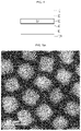
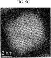
- the c may be a length of a longer side length.
- the two dimensional image may be a high resolution transmission electron microscopy image wherein a resolution may be from about 0.2 nm to about 0.08 nm and the magnification may be from about x2,000,000 to about x10,000,000, about x3,000,000 to about x7,000,000, for example, 5,000,000 times.
- High-resolution transmission electron microscopy is an imaging mode of specialized transmission electron microscopes that allows for direct imaging of the atomic structure of a given nanostructure.
- the HRTEM is substantially identical to transmission electron microscopy (TEM) imaging except that the magnifications used are high enough to see the lattice spacing of inorganic materials (typically on the order of several angstroms ( ⁇ )). Although such lattice spacings can easily be recorded onto film at moderate magnifications. The cubicity will be further explained in reference to FIG. 1 .
- an electroluminescent device may include a first electrically conducting layer (e.g., a first electrode, as used herein the electrically conducting layer and the electrode are terms that can be interchangeably used), a second electrically conducting layer (e.g., a second electrode), for example, spaced from one another or facing each other, and a light-emitting layer (e.g., a light emitting film, as used herein, the phrases “light emitting layer” and “light emitting film” can be used interchangeably) disposed between the first electrically conducting layer and the second electrically conducting layer and including light emitting nanostructures.
- a first electrically conducting layer e.g., a first electrode, as used herein the electrically conducting layer and the electrode are terms that can be interchangeably used
- a second electrically conducting layer e.g., a second electrode
- a light-emitting layer e.g., a light emitting film, as used herein, the phrases “light emitting layer” and “light emitting film” can
- the light emitting device may exhibit a maximum EQE of greater than or equal to about 10%, and the light emitting device may show, e.g., exhibit, a maximum luminance of greater than or equal to about 300,000 cd/m 2 .
- the light emitting nanostructures may include a first semiconductor nanocrystal including a Group III-V compound and a second semiconductor nanocrystal including a zinc chalcogenide, wherein the Group III-V compound includes indium, phosphorus, and optionally zinc, and the zinc chalcogenide include zinc, selenium, and sulfur.
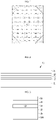
- FIG. 2 is a cross-sectional representation of a light-emitting device according to an embodiment.
- the light-emitting device 10 according to an embodiment includes electrodes (first electrode 11 and second electrode 15) spaced apart and each with a surface opposite the other, and a light-emitting layer 13 including a plurality of quantum dots disposed between the electrodes.
- a charge auxiliary layer may be disposed between the light-emitting layer 13 and the electrodes.
- first electrode 11 is an anode and the second electrode 15 is a cathode
- a hole auxiliary layer 12 that assists movement (transport/injection) of holes may be disposed between the first electrically conducting layer and the light-emitting layer and an electron auxiliary layer 14 that assists movement (transport/injection) of electrons may be disposed between the second electrically conducting layer and the light-emitting film.
- the light-emitting device may include a substrate (not shown).
- the substrate may be disposed on the first electrode 11 (e.g., a major surface of the first electrode 11) or may be disposed on the second electrode 15 (e.g., a major surface of the second electrode 15).
- the substrate may be disposed on an opposite side of the first electrically conducting layer (e.g., under the first electrically conducting layer) in FIG. 2 .
- the substrate may be disposed on an opposite side of the second electrode 15 (e.g., above the second electrically conducting layer) in FIG 2 .
- the substrate may be a substrate including an insulation material (e.g., insulating transparent substrate).
- the substrate may include glass; various polymers such as polyester (e.g., polyethylene terephthalate (PET), polyethylene naphthalate (PEN)), polycarbonate, poly(meth)acrylate, polyimide, and poly(amide-imide); polysiloxane (e.g., polydimethylsiloxane (PDMS)); inorganic materials such as silicon, silicon oxide, and Al 2 O 3 ; or a combination thereof, but is not limited thereto.
- polyester e.g., polyethylene terephthalate (PET), polyethylene naphthalate (PEN)
- PET polyethylene naphthalate
- PEN polycarbonate
- poly(meth)acrylate polyimide
- poly(amide-imide) poly(amide-imide)
- polysiloxane e.g., polydimethylsiloxane (PDMS)
- inorganic materials such as silicon, silicon oxide, and Al 2 O 3 ; or a combination thereof, but is not limited there
- transparent refers to transmittance for light in a predetermined wavelength (e.g., light emitted from the quantum dots) of greater than or equal to about 85%, for example, greater than or equal to about 88%, greater than or equal to about 90%, greater than or equal to about 95%, greater than or equal to about 97%, or greater than or equal to about 99%.
- a thickness of the substrate may be appropriately selected considering a substrate material, and the like, but is not particularly limited.
- the transparent substrate may have flexibility.
- the substrate may be omitted.
- One of the first electrode 11 or the second electrode 15 may be an anode and the other may be a cathode.
- the first electrode 11 may be an anode
- the second electrode 15 may be a cathode and vice versa.
- the first electrode 11 may be made of a conductor, for example a metal, a conductive metal oxide, or a combination thereof.
- the first electrode 11 may be for example made of a metal, such as nickel, platinum, vanadium, chromium, copper, zinc, and gold, or an alloy thereof; a conductive metal oxide, such as zinc oxide, indium oxide, tin oxide, indium tin oxide (ITO), indium zinc oxide (IZO), or fluorine doped tin oxide; or a combination of metal and oxide, such as ZnO and Al or SnO 2 and Sb; and the like, but is not limited thereto.
- the first electrically conducting layer may include a transparent conductive metal oxide, for example, indium tin oxide.
- a work function of the first electrically conducting layer may be higher than a work function of the second electrically conducting layer that will be described herein.
- a work function of the first electrically conducting layer may be lower than a work function of the second electrically conducting layer that will be described herein.
- the second electrode 15 may be made of a conductor, for example a metal, a conductive metal oxide, a conductive polymer, or a combination thereof.
- the second electrode 15 may be for example a metal, such as aluminum, magnesium, calcium, sodium, potassium, titanium, indium, yttrium, lithium, gadolinium, silver, tin, lead, cesium, or barium, or an alloy thereof; a multi-layer structured material, such as LiF/AI, Li 2 O/Al, Liq/AI, LiF/Ca, and BaF 2 /Ca, but is not limited thereto.
- the second electrically conducting layer may include a transparent conductive metal oxide, such as indium tin oxide.
- the conductive metal oxide is the same as described herein.
- a work function of the first electrode 11 may be from about 4.5 eV to about 5.0 eV (e.g., from about 4.6 eV to about 4.9 eV), and a work function of the second electrode 15 may be greater than or equal to about 4.0 eV and less than or equal to about 4.8 eV (e.g., for example, from about 4.1 eV to about 4.7 eV, from about 4.3 eV to about 4.5 eV).
- a work function of the second electrode 15 may be from about 4.5 eV to about 5.0 eV (e.g., from about 4.6 eV to about 4.9 eV), and a work function of the first electrode 11 may be greater than or equal to about 4.0 eV and less than or equal to about 4.8 eV (e.g., for example, from about 4.1 eV to about 4.7 eV, from about 4.3 eV to about 4.5 eV).
- the first electrode 11, the second electrode 15, or each of the first electrode 11 and the second electrode 15 may be a light-transmitting electrode, and the light-transmitting electrode may be for example made of a conductive oxide such as a zinc oxide, indium oxide, tin oxide, indium tin oxide (ITO), indium zinc oxide (IZO), or fluorine doped tin oxide, or a metal thin layer of a single layer or a multilayer. If one of the first electrode 11 or the second electrode 15 is a non-light-transmitting electrode, the electrode may be made of for example an opaque conductor such as aluminum (Al), silver (Ag), or gold (Au).
- a thickness of the electrodes is not particularly limited and may be appropriately selected considering device efficiency.
- the thickness of the electrodes may greater than or equal to about 5 nanometers (nm), for example, greater than or equal to about 50 nm, or greater than or equal to about 100 nm.
- the thickness of the electrodes may be less than or equal to about 100 ⁇ m, for example, less than or equal to about 10 um, less than or equal to about 1 um, less than or equal to about 900 nm, less than or equal to about 500 nm, less than or equal to about 400 nm, less than or equal to about 300 nm, less than or equal to about 200 nm, or less than or equal to about 100 nm.
- the emissive layer 13 includes (e.g., a plurality of) light emitting nanostructures.
- a light emitting nanostructure such as a quantum dot or a semiconductor nanocrystal may absorb energy (e.g., an electrical energy or a photo-energy) from an excitation source to be excited and may emit light of a wavelength corresponding to a bandgap energy thereof.
- the bandgap energy of the light emitting nanostructure may vary with a size, composition, or a combination thereof of the nanocrystal.
- the light emitting nanostructures may have a narrower bandgap energy, and an increased luminous wavelength as their sizes increase.
- the light emitting nanostructures draw attention and find their use as a light emitting material in various fields such as a display device, an energy device, or a bio light emitting device.
- the light emitting nanostructures such as a quantum dot may achieve increased light emitting efficiency and improved color reproducibility.
- a light emitting device using electrical energy as an excitation source (hereinafter, which can be referred to as an electroluminescent device) or a display device including the same may be driven without an external light source.
- the electrical conductor e.g., a first electrode and a second electrode
- the electrical conductor may provide electrons and holes, which are injected into a light emitting layer and recombined therein to form exciton and from the exciton, an energy can be emit in a form of light.
- Quantum dots including a toxic heavy metal such as cadmium, lead, mercury, or a combination thereof may show, e.g., exhibit, better properties and greater stability than a cadmium free quantum dot.
- cadmium may cause environment/health problems and is one of the restricted elements via Restriction of Hazardous Substances Directive (RoHS) in many countries.
- RoHS Restriction of Hazardous Substances Directive
- development of a cadmium-free quantum dot that may exhibit improved electroluminescence properties (e.g., when being used in an electroluminescent device) such as a desired wavelength, a narrowed full width at half maximum (FWHM), and increased luminance can be a challenging task in the art.
- a nanostructure or a semiconductor nanocrystal particle (also referred to as "quantum dot” herein) including a Group III-V compound may be a cadmium free light emitting nanostructure that may be applied, e.g., used, in a variety of electronic devices such as a display device for example, in a form of a film.
- quantum dot indium phosphide based quantum dots may be desired to have a tiny size of less than about 7 nm for green light emission.
- the indium phosphide based quantum dots emitting green light may not achieve a desired level of electroluminescent properties. Without wishing to be bound by any theory, it is believed that such a small size desired for green light emission may include a relatively large surface area and a presence of a relatively large amount of an organic ligand thereon. Without wishing to be bound any theory, it is believed that unlike a photoluminescent type device using light as an excitation source, in the electroluminescent device, such a large amount of the organic ligand may play a considerable role of resistance, whereby the properties of the device can be limited and the durability of the device may also be adversely affected.
- an indium phosphide based quantum dot including a relatively increased size and emitting green light may tend to have a distorted particle shape and it may be difficult to achieve a uniform particle size distribution.
- the present inventors have found that the large sized quantum dots including an indium phosphide and emitting green light may not show, e.g., exhibit, a desired level of properties such as the emission efficiency, luminance, and reliability at the same time even when the large sized quantum dots including an indium phosphide and emitting green light show, e.g., exhibit, enhanced properties in a solution state.
- the second semiconductor nanocrystal e.g., a shell
- the second semiconductor nanocrystal e.g., a shell
- a decrease in an amount of the second semiconductor nanocrystal may cause an adverse effect on a particle size distribution and a luminous property thereof, while an increase in the amount of the second semiconductor nanocrystal may lead to a shape distortion due to a difference of a crystal growth rate and a lattice mismatch. Accordingly, there still remains much room for improvement of properties for an electroluminescent device including conventional quantum dots emitting green light.
- the light emitting nanostructure may be prepared by a method disclosed herein (for example, involving an increased reaction temperature and a controlled manner in terms of injection times and an amount of precursor for each injection).
- a particle growth may be accomplished in a same crystal plane substantially without a defect.
- a mole ratio between the first semiconductor nanocrystal and the second semiconductor nanocrystal or a mole ratio between the zinc chalcogenides may be controlled to change the lattice strain and the lattice mismatch.
- the nanostructures prepared therefrom may exhibit an increased cubic shaped feature (e.g., increased cubicity or squareness), and this shape feature is believed to result in the improvement of the electroluminescent properties in the application for the device.
- the light emitting device includes a light emitting film including light emitting nanostructure including an indium phosphide and may achieve an improved level of properties for an electroluminescent device at the same time.
- the light emitting nanostructures may include a first semiconductor nanocrystal including a Group III-V compound and a second semiconductor nanocrystal including a zinc chalcogenide.
- the Group III-V compound may include indium, phosphorus, and optionally zinc.
- the zinc chalcogenide include zinc, selenium, and sulfur.
- the light emitting nanostructures may exhibit a zinc blende structure and may show, e.g., exhibit, a cubic shaped feature.
- a transmission electron microscopy analysis is carried out to obtain a two dimensional image of each of the given particle(s), using a commercially available TEM equipment.
- An area of the given particle A or a total area of the given particles A' in the two dimensional TEM image may be easily and readily calculated, respectively, for example, by using a commercially available image analysis program such as image J or an image handling program for example, universally available or compatible with operating system or hardware, such as "Paint" from Microsoft Windows.
- the area corresponding to (100) plane can be calculated using a high resolution transmission electron microscope and determine an area B of crystal domain region observed in a direction of 100 (e.g., [100] direction).
- the area B is divided with the area A' to provide the cubicity (see FIG. 1 ).
- the smallest square that covers the area of a given light emitting nanostructure e.g., a circumscribed square
- the C may be calculated by c 2 wherein c is a length of the smallest square.
- the smallest square may be readily and reproducibly determined for each of the particles in any commercially available image handling computer program (for example, universally provided by Microsoft Windows).
- the area A is divided with the area C to provide the squareness.
- the light emitting nanostructures have a first semiconductor nanocrystal of InP or InZnP and a second semiconductor nanocrystal including a zinc chalcogenide, for example, in a core shell structure, and by adopting the preparation method disclosed herein, the light emitting nanostructures show, e.g., exhibit, an increased cubic shaped feature (e.g., a squareness or a cubicity) disclosed herein even together with an increased size.
- an increased cubic shaped feature e.g., a squareness or a cubicity
- a growth rate may vary with a site in a given particle as an amount of the second semiconductor nanocrystal and this may result in a shape distortion for example due to a lattice mismatch between the first semiconductor nanocrystal and the second semiconductor nanocrystal.
- the quantum dots including InP e.g., InZnP
- emitting green light may show, e.g., exhibit, an increased solidity or circularity in light of a shape factor but even with the increased solidity or circularity, the green light emitting quantum dots may not show, e.g., exhibit, a desired level of the combination of the electroluminescent properties (e.g., a high EQE and a high luminance) when being applied, e.g., used, in an electroluminescent device.
- the solidity and the circularity are a shape factor that is universally defined and can be readily and reproducibly determined by using an image analysis program or code.
- the circularity may be determined by using a two dimensional image obtained by an electron microscopy analysis and using the following equation referring to image J user guide (v 1.46r): 4 ⁇ x Area / Perimeter 2
- the circularity may be 1 for a perfect circle and as the circularity is closer to zero (0), a given shape is an increasingly elongated shape.
- a solidity of a nanostructure can be determined by dividing "a measured area" of the nanostructure with "a convex hull area” in a TEM analysis thereof.
- the convex hull may be defined as the smallest convex set of points in which a set of all points constituting a two dimensional image of a given quantum dot obtained by an electron microscopic analysis is contained.
- the indium phosphide based nanostructures may achieve the combined electroluminescent properties that are improved to a desired level in an electroluminescent device.
- the aforementioned nanostructures may be obtained by the method disclosed herein.
- the synthesis of the aforementioned nanostructures may involve changing (e.g., increasing) a temperature for the formation of the second semiconductor nanocrystal and adopting an intermittent injection manner of precursors for the second semiconductor nanocrystal several times (e.g., at least two times, three times, or more) optionally wherein an injection amount for each precursor is changed (e.g., increased) and whereby the formation or the growth of the nanocrystal occurs on a desired crystal facet (e.g., the same crystal facet).
- a desired crystal facet e.g., the same crystal facet
- the nanocrystal structures included in the light emitting layer of the device of an embodiment include the first semiconductor nanocrystal and the second semiconductor nanocrystal in such a manner that a lattice strain and a lattice mismatch between the first semiconductor nanocrystal and the second semiconductor nanocrystal or between the zinc selenide and the zinc sulfide included in the second semiconductor nanocrystal may be controlled within a desired extent and thus the resulting nanocrystal structures may show, e.g., exhibit, the cubic shaped features (e.g., the squareness or the cubicity) that cannot be achieved for conventional green light emitting, indium phosphide based nanostructures.
- the cubic shaped features e.g., the squareness or the cubicity
- the nanocrystal structures thus obtained may emit green light while having relatively increased sizes together with an improved particle size distribution.
- the nanostructures of an embodiment having the composition disclosed herein may exhibit the cubic shaped features (e.g., the squareness or the cubicity) for example together with a relatively increased size, an improved particle size distribution, or a combination thereof, achieving a desired level of the combined electroluminescent properties (e.g., the max EQE and max luminance) when being included in an electroluminescent device.
- the nanostructures of an embodiment may form the light emitting layer or the light emitting film to have an increased packing density, which may further contribute to achieving the desired combination of the electroluminescent properties.
- the cubic shaped feature e.g., the cubicity of the light emitting structures may be greater than or equal to about 0.7, greater than or equal to about 0.71, greater than or equal to about 0.72, greater than or equal to about 0.73, greater than or equal to about 0.74, greater than or equal to about 0.75, greater than or equal to about 0.76, greater than or equal to about 0.77, greater than or equal to about 0.78, greater than or equal to about 0.79, greater than or equal to about 0.8, greater than or equal to about 0.81, greater than or equal to about 0.82, greater than or equal to about 0.83, greater than or equal to about 0.84, greater than or equal to about 0.85, greater than or equal to about 0.86, greater than or equal to about 0.87, greater than or equal to about 0.88, greater than or equal to about 0.89, or greater than or equal to about 0.9.
- the cubicity of the light emitting structures may be less than or equal to about 1, less than or equal to about 0.99, less than or equal to about 0.98, less than or equal to about 0.97, less than or equal to about 0.96, or less than or equal to about 0.95.
- the squareness of the light emitting structures may be greater than or equal to about 0.8, greater than or equal to about 0.81, greater than or equal to about 0.82, greater than or equal to about 0.83, greater than or equal to about 0.84, greater than or equal to about 0.85, greater than or equal to about 0.86, greater than or equal to about 0.87, greater than or equal to about 0.88, greater than or equal to about 0.89, or greater than or equal to about 0.9.
- the squareness of the light emitting structures may be less than or equal to about 1, less than or equal to about 0.99, less than or equal to about 0.98, less than or equal to about 0.97, less than or equal to about 0.96, or less than or equal to about 0.95.
- the light emitting nanostructures may be configured to emit green light while having an increased average size.
- the average size of the light emitting nanostructures may be greater than or equal to about 7 nm, greater than or equal to about 7.1 nm, greater than or equal to about 7.2 nm, greater than or equal to about 7.3 nm, greater than or equal to about 7.4 nm, greater than or equal to about 7.5 nm, greater than or equal to about 7.6 nm, greater than or equal to about 7.7 nm, greater than or equal to about 7.8 nm, greater than or equal to about 7.9 nm, greater than or equal to about 8 nm, greater than or equal to about 8.1 nm, greater than or equal to about 8.2 nm, greater than or equal to about 8.3 nm, greater than or equal to about 8.4 nm, greater than or equal to about 8.5 nm, greater than or equal to about 8.6 nm, greater than or equal to about 8.7 nm
- the average size of the light emitting nanostructures may be less than or equal to about 20 nm, less than or equal to about 19 nm, less than or equal to about 18 nm, less than or equal to about 17 nm, less than or equal to about 16 nm, less than or equal to about 15 nm, less than or equal to about 14 nm, less than or equal to about 13 nm, less than or equal to about 12 nm, less than or equal to about 11 nm, or less than or equal to about 10 nm.
- the light emitting structures may show, e.g., exhibit, a relatively uniform particle size distribution, which may be less than or equal to about 10%, less than or equal to about 9%, less than or equal to about 8%, or less than or equal to about 7% of the average size thereof.
- the light emitting nanostructures may have a surface predominant with (100) face of the crystal, and in the light emitting device or in the light emitting film, the light emitting structures of an embodiment may have the predominant crystal facet on a surface thereof, whereby surface properties (e.g., a metal rich surface or an organic ligand rich surface) of the light emitting nanostructures may become more uniform.
- surface properties e.g., a metal rich surface or an organic ligand rich surface
- the nanostructures may be prepared with a process enabling a crystal growth at a controlled crystal facet, which may reduce a lattice defect and achieve a crystallographically improved quality.
- the improved crystal quality may affect the luminance properties of the quantum dots, and may be translated into a suppressed/limited surface trap emission.
- the trap emission refers to an emission other than the band edge mission (i.e., the luminous emission involved in the balance band and the conduction band).
- the degree of the trap emission may be confirmed by a low temperature photoluminescent analysis (e.g., carried out at a temperature of about 77 K).
- the nanocrystals of an embodiment may exhibit a full width at half maximum of less than or equal to about 11 nm, less than or equal to about 10 nm, less than or equal to about 9 nm, or less than or equal to about 8 nm.
- a mole ratio of zinc with respect to indium may be greater than about 39:1, greater than or equal to about 40:1, greater than or equal to about 41:1, greater than or equal to about 42:1, greater than or equal to about 43:1, greater than or equal to about 44:1, greater than or equal to about 45:1, greater than or equal to about 46:1, greater than or equal to about 47:1, greater than or equal to about 48:1, greater than or equal to about 49:1, greater than or equal to about 50:1, greater than or equal to about 51:1, greater than or equal to about 52:1, greater than or equal to about 53:1, greater than or equal to about 54:1, greater than or equal to about 55:1, or greater than or equal to about 56:1.
- the mole ratio of zinc with respect to indium may be less than or equal to about 92:1, less than or equal to about 91:1, less than or equal to about 90:1, less than or equal to about 89:1, less than or equal to about 85:1, less than or equal to about 80:1, less than or equal to about 75:1, less than or equal to about 70:1, less than or equal to about 69:1, less than or equal to about 68:1, less than or equal to about 67:1, less than or equal to about 66:1, less than or equal to about 65:1, less than or equal to about 64:1, less than or equal to about 63:1, less than or equal to about 62:1, less than or equal to about 61:1, less than or equal to about 60:1, or less than or equal to about 59:1.
- the mole ratio of zinc with respect to indium (Zn:ln) may be greater than or equal to about 43. In an embodiment, the mole ratio of zinc with respect to indium (Zn:ln) may be greater than or equal to about 49:1, greater than or equal to about 50:1, greater than or equal to about 50.5:1, greater than or equal to about 51:1, or greater than or equal to about 52:1. In an embodiment, the mole ratio of zinc with respect to indium (Zn:ln) may be from about 49:1 to about 65:1, from about 49.5:1 to about 63.5:1, from about 55:1 to about 63:1, from about 57:1 to about 62.5:1, or a combination thereof.
- An amount of components included in the quantum dot as described herein may be determined through, e.g., with, an appropriate analysis tool (e.g., an inductively coupled plasma atomic emission spectroscopy (ICP-AES), an X-ray photoelectron spectroscopy (XPS), an ion chromatography, a Transmission electron microscopy energy-dispersive X-ray spectroscopy (TEM-EDS), or the like).
- an appropriate analysis tool e.g., an inductively coupled plasma atomic emission spectroscopy (ICP-AES), an X-ray photoelectron spectroscopy (XPS), an ion chromatography, a Transmission electron microscopy energy-dispersive X-ray spectroscopy (TEM-EDS), or the like.
- a mole ratio of sulfur with respect to indium may be greater than or equal to about 11:1, greater than or equal to about 11.5:1, greater than or equal to about 12:1, greater than or equal to about 12.3:1, or greater than or equal to about 12.5:1.
- the mole ratio of sulfur with respect to indium (S:In) may be less than or equal to about 19:1, less than or equal to about 18:1, less than or equal to about 17:1, less than or equal to about 16:1, less than or equal to about 15:1, less than or equal to about 14:1, less than or equal to about 13.5:1, less than or equal to about 13:1, less than or equal to about 12.8:1, or less than or equal to about 12.5:1.
- a mole ratio of selenium with respect to indium may be greater than or equal to about 29:1, greater than or equal to about 30:1, greater than or equal to about 35:1, greater than or equal to about 37:1, greater than or equal to about 37.5:1, greater than or equal to about 38:1, greater than or equal to about 38.5:1, or greater than or equal to about 39:1.
- a mole ratio of selenium with respect to indium may be less than or equal to about 75:1, less than or equal to about 74:1, less than or equal to about 73:1, less than or equal to about 72:1, less than or equal to about 71:1, less than or equal to about 70:1, less than or equal to about 69:1, less than or equal to about 68:1, less than or equal to about 67:1, less than or equal to about 66:1, less than or equal to about 65:1, less than or equal to about 64:1, less than or equal to about 63:1, less than or equal to about 62:1, less than or equal to about 61:1, less than or equal to about 60:1, less than or equal to about 59:1, less than or equal to about 58:1, less than or equal to about 57:1, less than or equal to about 56:1, less than or equal to about 55:1, less than or equal to about 54:1, less than or equal to about 53:1, or less than or equal to about 52
- a mole ratio of indium with respect to a total sum of sulfur and selenium ⁇ In:(Se+S) ⁇ may be less than or equal to about 0.04:1, less than or equal to about 0.039:1, less than or equal to about 0.038:1, less than or equal to about 0.037:1, less than or equal to about 0.036:1, less than or equal to about 0.035:1, less than or equal to about 0.034:1, less than or equal to about 0.033:1, less than or equal to about 0.032:1, less than or equal to about 0.031:1, less than or equal to about 0.03:1, less than or equal to about 0.029:1, less than or equal to about 0.028:1, less than or equal to about 0.027:1, less than or equal to about 0.026:1, less than or equal to about 0.025:1, less than or equal to about 0.024:1, or less than or equal to about 0.0235:1.
- the mole ratio of indium with respect to a total sum of sulfur and selenium ⁇ In:(Se+S) ⁇ may be greater than or equal to about 0.001:1, greater than or equal to about 0.005:1, greater than or equal to about 0.01:1, or greater than or equal to about 0.015:1.
- a mole ratio of zinc with respect to a total sum of sulfur and selenium ⁇ Zn:(Se+S) ⁇ may be less than or equal to about 2:1, less than or equal to about 1.9:1, less than or equal to about 1.8:1, less than or equal to about 1.7:1, less than or equal to about 1.6:1, less than or equal to about 1.5:1, less than or equal to about 1.4:1, less than or equal to about 1.3:1, less than or equal to about 1.2:1, less than or equal to about 1.19:1, less than or equal to about 1.18:1, less than or equal to about 1.17:1, less than or equal to about 1.16:1, less than or equal to about 1.15:1, less than or equal to about 1.14:1, less than or equal to about 1.13:1, less than or equal to about 1.12:1, or less than or equal to about 1.1:1.
- a mole ratio of sulfur with respect to selenium may be less than or equal to about 0.5:1, less than or equal to about 0.49:1, less than or equal to about 0.48:1, less than or equal to about 0.47:1, less than or equal to about 0.46:1, less than or equal to about 0.45:1, less than or equal to about 0.44:1, less than or equal to about 0.43:1, less than or equal to about 0.42:1, less than or equal to about 0.41:1, less than or equal to about 0.4:1, less than or equal to about 0.39:1, less than or equal to about 0.38:1, less than or equal to about 0.37:1, less than or equal to about 0.36:1, less than or equal to about 0.35:1, less than or equal to about 0.34:1, less than or equal to about 0.33:1, or less than or equal to about 0.32:1.
- a mole ratio of sulfur with respect to selenium may be greater than or equal to about 0.15:1, greater than or equal to about 0.2:1, greater than or equal to about 0.21:1, greater than or equal to about 0.22:1, greater than or equal to about 0.23:1, greater than or equal to about 0.24:1, greater than or equal to about 0.25:1, greater than or equal to about 0.26:1, greater than or equal to about 0.27:1, or greater than or equal to about 0.28:1.
- At least a portion of (or an entire of) the surface of the core (e.g., the first semiconductor nanocrystal) of the light emitting nanostructures may include the second semiconductor nanocrystal.
- the entire of the surface of the core may include the second semiconductor nanocrystal.
- the light emitting nanostructures or the quantum dots may have a core shell structure including a core and a shell disposed on the core.
- the first semiconductor nanocrystal may be included in the core and the second semiconductor nanocrystal may be included in the shell.
- the first semiconductor nanocrystal or the core(s) may include an indium phosphide, an indium zinc phosphide, or a combination thereof.
- the core may have a size (or an average size) of greater than or equal to about 1 nm, greater than or equal to about 1.5 nm, greater than or equal to about 2 nm, or greater than or equal to about 2.5 nm.
- the core may have a size (or an average size) of less than or equal to about 5 nm, less than or equal to about 4 nm, less than or equal to about 3.5 nm, less than or equal to about 3 nm, or less than or equal to about 2.7 nm.
- the second semiconductor nanocrystal or the shell may include a zinc selenide, a zinc sulfide, or a combination thereof.
- the second semiconductor nanocrystal or the shell may include a zinc selenide sulfide.
- the shell or each of the shell layers in the multi-layered shell may include a gradient alloy having a composition varying in a direction of a radius, e.g., a radial direction from the core toward an outermost surface of the quantum dot.
- the shell or the second semiconductor nanocrystal may have a concentration of sulfur increasing in a direction of a radius, e.g., a radial direction from the core toward an outermost surface of the nanostructure.
- a concentration of sulfur may increase in a direction of a radius, e.g., a radial direction from the core toward an outermost surface of the nanostructure.
- the shell may be a multi-layered shell including two or more layers. In the multi-layered shell, adjacent two layers may have different compositions from each other.
- the multi-layered shell may include a first shell layer including zinc, selenium, and optionally sulfur, and a second shell layer disposed on the first shell layer, having a different composition from the first shell layer, and including zinc, sulfur, and optionally selenium.
- the first shell layer may be disposed directly on the core.
- the first shell layer may include a zinc selenide.
- the second shell layer may include a zinc sulfide.
- the first shell layer may include ZnSe, ZnSeS, or a combination thereof.
- the first shell layer may or may not include sulfur.
- the second shell layer may include ZnS, ZnSeS, or a combination thereof.
- the second shell layer may be an outermost shell layer of the nanostructure.
- a thickness of the shell may be greater than or equal to about 1 nm, greater than or equal to about 1.5 nm, greater than or equal to about 2 nm, greater than or equal to about 2.3 nm, greater than or equal to about 2.5 nm, greater than or equal to about 2.7 nm, greater than or equal to about 3 nm, or greater than or equal to about 3.1 nm, or greater than or equal to about 3.3 nm.
- a thickness of the shell may be less than or equal to about 6 nm, less than or equal to about 5 nm, less than or equal to about 4 nm, or less than or equal to about 3.5 nm.
- a thickness of the first shell layer may be greater than or equal to about 0.3 nm, greater than or equal to about 0.5 nm, greater than or equal to about 0.7 nm, greater than or equal to about 0.9 nm, greater than or equal to about 1 nm, greater than or equal to about 1.1 nm, greater than or equal to about 1.3 nm, greater than or equal to about 1.5 nm, greater than or equal to about 1.7 nm, greater than or equal to about 1.9 nm, greater than or equal to about 2 nm, greater than or equal to about 2.1 nm, greater than or equal to about 2.3 nm, greater than or equal to about 2.5 nm, greater than or equal to about 2.7 nm, greater than or equal to about 2.9 nm, or greater than or equal to about 3 nm.
- a thickness of the first shell layer may be less than or equal to about 5 nm, less than or equal to about 4.5 nm, less than or equal to about 4 nm, less than or equal to about 3.5 nm, less than or equal to about 3 nm, or less than or equal to about 2.5 nm.
- a thickness of the second shell layer may be greater than or equal to about 0.3 nm, greater than or equal to about 0.5 nm, greater than or equal to about 0.7 nm, greater than or equal to about 0.9 nm, greater than or equal to about 1 nm, greater than or equal to about 1.1 nm, greater than or equal to about 1.3 nm, greater than or equal to about 1.5 nm, greater than or equal to about 1.7 nm, greater than or equal to about 1.9 nm, greater than or equal to about 2 nm, greater than or equal to about 2.1 nm, greater than or equal to about 2.3 nm, greater than or equal to about 2.5 nm, greater than or equal to about 2.7 nm, greater than or equal to about 2.9 nm, or greater than or equal to about 3 nm.
- a thickness of the second shell layer may be less than or equal to about 5 nm, less than or equal to about 4.5 nm, less than or equal to about 4 nm, less than or equal to about 3.5 nm, less than or equal to about 3 nm, less than or equal to about 2.5 nm, less than or equal to about 2 nm, less than or equal to about 1.5 nm, less than or equal to about 1 nm, less than or equal to about 0.7 nm, or less than or equal to about 0.5 nm.
- the first semiconductor nanocrystal or the core may not include manganese, copper, or a combination thereof.
- the first semiconductor nanocrystal or the core may or may not include tellurium.
- the light emitting nanostructures may emit green light.
- the wavelength of the green light may be disclosed herein.
- a quantum yield or efficiency of the light emitting nanostructures may be greater than or equal to about 70%, greater than or equal to about 71%, greater than or equal to about 72%, greater than or equal to about 73%, greater than or equal to about 74%, greater than or equal to about 75%, greater than or equal to about 76%, greater than or equal to about 77%, greater than or equal to about 78%, greater than or equal to about 79%, greater than or equal to about 80%, greater than or equal to about 81%, greater than or equal to about 82%, greater than or equal to about 83%, greater than or equal to about 84%, greater than or equal to about 85%, or greater than or equal to about 90%.
- the light emitting nanostructures or the light emitting layer (film) may exhibit a maximum luminescent peak having a full width at half maximum of less than or equal to about 45 nm, as measured at room temperature (e.g., about 20 °C to 25 °C).
- the full width at half maximum may be less than or equal to about 45 nm, less than or equal to about 44 nm, less than or equal to about 43 nm, less than or equal to about 42 nm, less than or equal to about 41 nm, less than or equal to about 40 nm, less than or equal to about 39 nm, less than or equal to about 38 nm, less than or equal to about 37 nm, less than or equal to about 36 nm, less than or equal to about 35 nm, less than or equal to about 34 nm, or less than or equal to about 33 nm.
- the light emitting nanostructures may be prepared by a method as described herein.
- the method includes: in the presence of a nanoparticle (e.g., including a core) that includes the first semiconductor nanocrystal and an organic ligand (e.g., in an organic solvent), reacting a zinc precursor, a selenium precursor, and a sulfur precursor at a temperature of greater than about 320 °C, for example, greater than or equal to about 330 °C, greater than or equal to about 335 °C, or greater than or equal to about 340 °C to form a second semiconductor nanocrystal, wherein the selenium precursor and optionally the sulfur precursor are added or injected in a split manner (e.g., not all at once), intermittently to a reaction medium at least two times, in a different aliquot each time, respectively, optionally together with a zinc precursor.
- a split manner e.g., not all at once
- the selenium precursor and the sulfur precursor may be added separately.
- the selenium precursor and the sulfur precursor may be added without being mixed together.
- a predetermined amount of the selenium precursor is added first and then addition of the sulfur precursor (for example in the split manner) to the reaction medium may be started.
- the selenium precursor may be added at least twice, at least three times, or at least four times in a different aliquot each time.
- a second aliquot added secondly may be greater than a first aliquot added firstly.
- a third aliquot added thirdly may be greater than a second aliquot added secondly.
- the sulfur precursor may be added once or at least twice, at least three times, or at least four times in the same aliquot or in different aliquots each time.
- a second aliquot added secondly may be greater than a first aliquot added firstly.
- a third aliquot added thirdly may be greater than a second aliquot added secondly.
- an aliquot added each time may be controlled taking into consideration the types of the precursors, a reaction temperature, and a desired composition of the light emitting nanostructures.
- controlling the manner (e.g., in terms of the amount and the number of times) of adding the precursors for the formation of the second semiconductor nanocrystal as described herein may minimize the difference that can occur otherwise depending on the growth site of the nanostructure, and this can also suppress the shape distortion for example due to the lattice mismatch between the zinc selenide and the zinc sulfide.
- the nanostructures prepared by the method disclosed herein may show, e.g., exhibit, the cubicity or the squareness together with a relatively increased size and a uniform size distribution.
- the first semiconductor nanocrystal may be prepared in an appropriate manner.
- the core may be commercially available or may be prepared by any proper method.
- the core may be synthesized in a hot injection manner wherein a solution including a metal precursor (e.g., an indium precursor) and optionally a ligand is heated at a high temperature (e.g., of greater than or equal to about 200 °C) and then a phosphorous precursor is injected into the heated hot solution.
- a metal precursor e.g., an indium precursor
- a ligand is heated at a high temperature (e.g., of greater than or equal to about 200 °C) and then a phosphorous precursor is injected into the heated hot solution.
- the zinc precursor may include a Zn metal powder, an alkylated Zn compound, Zn alkoxide, Zn carboxylate, Zn nitrate, Zn perchlorate, Zn sulfate, Zn acetylacetonate, Zn halide (e.g., zinc chloride), Zn cyanide, Zn hydroxide, Zn oxide, Zn peroxide, Zn carbonate, or a combination thereof.
- Zn metal powder an alkylated Zn compound, Zn alkoxide, Zn carboxylate, Zn nitrate, Zn perchlorate, Zn sulfate, Zn acetylacetonate, Zn halide (e.g., zinc chloride), Zn cyanide, Zn hydroxide, Zn oxide, Zn peroxide, Zn carbonate, or a combination thereof.
- Examples of the zinc precursor may include dimethyl zinc, diethyl zinc, zinc acetate, zinc acetylacetonate, zinc iodide, zinc bromide, zinc chloride, zinc fluoride, zinc carbonate, zinc cyanide, zinc nitrate, zinc oxide, zinc peroxide, zinc perchlorate, zinc sulfate, and the like.
- the selenium precursor may include selenium-trioctyl phosphine (Se-TOP), selenium-tributylphosphine (Se-TBP), selenium-triphenylphosphine (Se-TPP), or a combination thereof, but is not limited thereto.
- the sulfur precursor may include hexane thiol, octane thiol, decane thiol, dodecane thiol, hexadecane thiol, mercapto propyl silane, sulfur-trioctyl phosphine (S-TOP), sulfur-tributylphosphine (S-TBP), sulfur-triphenylphosphine (S-TPP), sulfur-trioctylamine (S-TOA), bis(trimethylsilyl)methyl sulfide, bis(trimethylsilyl)sulfide, ammonium sulfide, sodium sulfide, or a combination thereof.
- the sulfur precursor may be injected once or at least twice.
- the organic solvent may be a C6 to C22 primary amine such as hexadecylamine; a C6 to C22 secondary amine such as dioctylamine; a C6 to C40 tertiary amine such as trioctylamine; a nitrogen-containing heterocyclic compound such as pyridine; a C6 to C40 aliphatic hydrocarbon (e.g., alkane, alkene, alkyne, etc.) such as hexadecane, octadecane, octadecene, or squalane; a C6 to C30 aromatic hydrocarbon such as phenyldodecane, phenyltetradecane, or phenyl hexadecane; a phosphine substituted with a C6 to C22 alkyl group such as trioctyl phosphine; a phosphine oxide substituted with a C6 to C22 alky
- the organic ligand may coordinate to a surface of the light emitting nanostructures thus prepared.
- the organic ligand may help the dispersibility of the nanostructures in an organic medium (e.g., an organic solution).
- the organic ligand may include RCOOH, RNH 2 , R 2 NH, R 3 N, RSH, RH 2 PO, R 2 HPO, R 3 PO, RH 2 P, R 2 HP, R 3 P, ROH, RCOOR', RPO(OH) 2 , RHPOOH, R 2 POOH (wherein, R and R' are independently a C1 to C40 (or C3 to C24) aliphatic hydrocarbon group (e.g., alkyl group, alkenyl group alkynyl group), or C6 to C40 (or C6 to C24) aromatic hydrocarbon group (e.g., C6 to C20 aryl group)), or a combination thereof.
- the organic ligand may be used alone or as a mixture of two or more.
- Examples of the organic ligand may include methane thiol, ethane thiol, propane thiol, butane thiol, pentane thiol, hexane thiol, octane thiol, dodecane thiol, hexadecane thiol, octadecane thiol, benzyl thiol; methane amine, ethane amine, propane amine, butyl amine, pentyl amine, hexyl amine, octyl amine, dodecyl amine, hexadecyl amine, octadecyl amine, dimethyl amine, diethyl amine, dipropyl amine; methanoic acid, ethanoic acid, propanoic acid, butanoic acid, pentanoic acid, hexanoic acid, hepta
- reaction conditions such as a reaction time, a reaction temperature, and the like may be selected appropriately taking into consideration a desired composition of the nanostructure.
- heating (or vacuum treating) a zinc precursor and an organic solvent and optionally an organic ligand at a predetermined temperature (e.g., at a temperature of greater than or equal to about 100 °C) under vacuum, and then changing an atmosphere of a reaction system into an inert gas and heating the same at a predetermined temperature (e.g., at a temperature of greater than or equal to about 100 °C) may be carried out.
- the particles including the first semiconductor nanocrystal may be added thereto and the precursors for the second semiconductor nanocrystal (i.e., the selenium precursor, the sulfur precursor, and optionally the zinc precursor) may be added in the manner as disclosed herein to carry out the reaction for the formation of the second semiconductor nanocrystal.
- the precursors for the second semiconductor nanocrystal i.e., the selenium precursor, the sulfur precursor, and optionally the zinc precursor
- the zinc precursor and the selenium precursor may be reacted to form a first shell layer and then the zinc precursor and the sulfur precursor may be reacted to form a second shell layer.
- the reaction temperature may be greater than about 320 °C, greater than or equal to about 325 °C, greater than or equal to about 330°C, greater than or equal to about 335°C, or greater than or equal to about 340 °C.
- the reaction temperature may be less than or equal to about 380 °C, less than or equal to about 370°C, less than or equal to about 360°C, or less than or equal to about 350 °C.
- an amount of each precursor and a concentration thereof may be selected taking into consideration a desired composition of the core and the shell, a reactivity between the core and shell precursors, or the like.
- a non-solvent may be added to reaction products and the light emitting nanostructures coordinated with, e.g., bound to, the ligand compound may be separated.
- the non-solvent may be a polar solvent that is miscible with the solvent used in the core formation reaction, shell formation reaction, or a combination thereof and is not capable of dispersing the produced nanocrystals therein.
- the non-solvent may be selected taking into consideration the solvent used in the reaction and may be for example acetone, ethanol, butanol, isopropanol, ethanediol, water, tetrahydrofuran (THF), dimethylsulfoxide (DMSO), diethyl ether, formaldehyde, acetaldehyde, a solvent having a similar solubility parameter to the foregoing non-solvents, or a combination thereof.
- Separation of the nanocrystal particles may involve centrifugation, sedimentation, chromatography, or distillation. The separated nanocrystal particles may be added to a washing (or dispersing) solvent and washed (or dispersed), if desired.
- Types of the washing (dispersing) solvent are not particularly limited and a solvent having similar solubility parameter to that of the ligand may be used and examples thereof may include hexane, heptane, octane, chloroform, toluene, benzene, or the like.
- the light emitting layer 13 may include a monolayer of quantum dots. In an embodiment, the light emitting layer 13 may include a monolayer of quantum dots, e.g., one or more, two or more, three or more, or four or more and 20 or less, 10 or less, 9 or less, 8 or less, 7 or less, or 6 or less, monolayers of quantum dots.
- the light emitting layer 13 may have a thickness of greater than or equal to about 5 nm, for example, greater than or equal to about 10 nm, greater than or equal to about 20 nm, or greater than or equal to about 30 nm and less than or equal to about 200 nm, for example, less than or equal to about 150 nm, less than or equal to about 100 nm, less than or equal to about 90 nm, less than or equal to about 80 nm, less than or equal to about 70 nm, less than or equal to about 60 nm, or less than or equal to about 50 nm.
- the light emitting layer 13 may have a thickness of, for example about 10 nm to about 150 nm, for example about 20 nm to about 100 nm, or for example about 30 nm to about 50 nm.
- the light emitting device may include a charge auxiliary layer (e.g., an electron auxiliary layer, a hole auxiliary layer, or a combination thereof) between the first electrically conducting layer and the second electrically conducting layer.
- the first electrode may be an anode, and a hole auxiliary layer 12 may be disposed between the first electrode 11 and the light emitting layer 13.
- the hole auxiliary layer 12 may have a layer, e.g., one or more layers, and may include, for example, a hole injection layer, a hole transport layer, an electron blocking layer (not shown), or a combination thereof.
- the HOMO energy level of the hole auxiliary layer 12 may be matched with the HOMO energy level of the light emitting layer 13, so that the mobility of holes transferred from the hole auxiliary layer 12 to the light emitting layer 13 may be enhanced.
- the hole auxiliary layer 12 may include a hole injection layer proximate to the first electrode 11 and a hole transport layer proximate to the light emitting layer 13.
- the hole auxiliary layer may include an organic compound.
- the organic compound may have a HOMO energy level of greater than or equal to about 5.0 eV, greater than or equal to about 5.1 eV, greater than or equal to about 5.2 eV, greater than or equal to about 5.3 eV, or greater than or equal to about 5.4 eV.
- the organic compound may have a HOMO energy level of less than or equal to about 5.5 eV, less than or equal to about 5.4 eV, less than or equal to about 5.3 eV, less than or equal to about 5.2 eV, or less than or equal to about 5.1 eV.
- a material of the hole auxiliary layer 12 is not particularly limited.
- the material of the hole auxiliary layer may include poly(9,9-dioctyl-fluorene-co-N-(4-butylphenyl)-diphenylamine) (TFB), polyarylamine, poly(N-vinylcarbazole) (PVK), poly(3,4-ethylenedioxythiophene (PEDOT), poly(3,4-ethylenedioxythiophene)polystyrene sulfonate (PEDOT:PSS), polyaniline, polypyrrole, N,N,N',N'-tetrakis(4-methoxyphenyl)-benzidine (TPD), 4,4'-bis[N-(1-naphthyl)-N-phenyl-amino]biphenyl (a-NPD), 4,4',4"-Tris[phenyl
- the electron blocking layer may include, for example, poly(3,4-ethylenedioxythiophene):poly(styrene sulfonate) (PEDOT:PSS), poly(9,9-dioctyl-fluorene-co-N-(4-butylphenyl)-diphenylamine) (TFB), polyarylamine, poly(N-vinylcarbazole), polyaniline, polypyrrole, N,N,N',N'-tetrakis(4-methoxyphenyl)-benzidine (TPD), 4,4'-bis[N-(1-naphthyl)-N-phenyl-amino]biphenyl (a-NPD), m-MTDATA, 4,4',4"-tris(N-carbazolyl)-triphenylamine (TCTA), or a combination thereof, but is not limited thereto.
- PEDOT:PSS poly(styrene sulf
- a thickness of each layer may be selected appropriately.
- a thickness of each layer may be greater than or equal to about 5 nm, greater than or equal to about 10 nm, greater than or equal to about 15 nm, or greater than or equal to about 20 nm and less than or equal to about 50 nm, less than or equal to about 40 nm, less than or equal to about 35 nm, or less than or equal to about 30 nm, but is not limited thereto.
- the second electrode may be a cathode
- the electron auxiliary layer 14 may be disposed between the light-emitting layer 13 and the second electrode 15.
- the electron auxiliary layer 14 may include, for example, an electron injecting layer, an electron transporting layer, a hole blocking layer, or a combination thereof.
- the electron auxiliary layer may be, for example, an electron injecting layer (EIL) that facilitates electron injection, an electron transporting layer (ETL) that facilitates electron transport, or a hole blocking layer (HBL) that blocks hole movement, or a combination thereof.
- EIL electron injecting layer
- ETL electron transporting layer
- HBL hole blocking layer
- an electron injecting layer may be disposed between the electron transport layer and the cathode.
- a hole blocking layer may be disposed between the light-emitting layer and the electron transporting (injecting) layer, but is not limited thereto.
- the thickness of each layer may be appropriately selected.
- the thickness of each layer may be greater than or equal to about 1 nm and less than or equal to about 500 nm, but is not limited thereto.
- the electron injecting layer may be an organic layer formed by deposition.
- the electron transporting layer may include inorganic oxide nanoparticles or be an organic layer formed by deposition.
- the electron transporting layer may include, for example, 1,4,5,8-naphthalene-tetracarboxylic dianhydride (NTCDA), bathocuproine (BCP), tris[3- (3-pyridyl)-mesityl]borane (3TPYMB), LiF, Alq 3 , Gaq 3 , Inq 3 , Znq 2 , Zn(BTZ) 2 , BeBq 2 , ET204 (8-(4-(4,6-di(naphthalen-2-yl)-1,3,5-triazin-2-yl)phenyl)quinolone), 8-hydroxyquinolinato lithium (Liq), n-type metal oxide (e.g., ZnO, HfO 2 , etc.), or a combination thereof, but is not limited thereto.
- NTCDA 1,4,5,8-naphthalene-tetracarboxylic dianhydride
- BCP bathocuproine
- TPYMB tris[3- (3
- the hole blocking layer may include, for example, 1,4,5,8-naphthalene-tetracarboxylic dianhydride (NTCDA), bathocuproine (BCP), tris[3-(3-pyridyl)-mesityl]borane (3TPYMB), LiF, Alq 3 , Gaq 3 , Inq 3 , Znq2, Zn(BTZ) 2 , BeBq 2 , or a combination thereof, but is not limited thereto.
- NTCDA 1,4,5,8-naphthalene-tetracarboxylic dianhydride
- BCP bathocuproine
- TPYMB tris[3-(3-pyridyl)-mesityl]borane
- the electronic auxiliary layer 14 may include a plurality of metal oxide nanoparticles.
- the nanoparticles may include a metal oxide including zinc.
- the metal oxide may include a zinc oxide, a zinc magnesium oxide, or a combination thereof.
- the metal oxide may include Zn 1-x M x O (wherein, M is Mg, Ca, Zr, W, Li, Ti, Y, Al, Co, or a combination thereof and 0 ⁇ x ⁇ 0.5).
- M may be magnesium (Mg).
- x may be greater than or equal to about 0.01 and less than or equal to about 0.3, for example, less than or equal to about 0.25, less than or equal to about 0.2, or less than or equal to about 0.15.
- an absolute value of LUMO of the aforementioned quantum dots included in the light-emitting layer may be smaller than the absolute value of LUMO of the metal oxide.
- the nanoparticles may have an average size of greater than or equal to about 1 nm, for example, greater than or equal to about 1.5 nm, greater than or equal to about 2 nm, greater than or equal to about 2.5 nm, or greater than or equal to about 3 nm and less than or equal to about 10 nm, less than or equal to about 9 nm, less than or equal to about 8 nm, less than or equal to about 7 nm, less than or equal to about 6 nm, or less than or equal to about 5 nm.
- the nanoparticles may not be rod-shaped or a nanowire.
- each thickness of the electron auxiliary layer 14 may be greater than or equal to about 5 nm, greater than or equal to about 6 nm, greater than or equal to about 7 nm, greater than or equal to about 8 nm, greater than or equal to about 9 nm, greater than or equal to about 10 nm, greater than or equal to about 11 nm, greater than or equal to about 12 nm, greater than or equal to about 13 nm, greater than or equal to about 14 nm, greater than or equal to about 15 nm, greater than or equal to about 16 nm, greater than or equal to about 17 nm, greater than or equal to about 18 nm, greater than or equal to about 19 nm, or greater than or equal to about 20 nm and less than or equal to about 120 nm, less than or equal to about 110 nm, less than or equal to about 100 nm, less than or equal to
- a device may have a normal structure.
- the device includes an anode 10 disposed on a transparent substrate 100, e.g., a metal oxide-based transparent electrode (e.g., ITO electrode) and a cathode 50 (e.g., facing the anode) may include a conductive metal (Mg, Al, etc.) (e.g., having a relatively low work function).
- a transparent substrate 100 e.g., a metal oxide-based transparent electrode (e.g., ITO electrode) and a cathode 50 (e.g., facing the anode)
- a conductive metal Mg, Al, etc.
- a hole auxiliary layer 20 (e.g., a hole injecting layer of, for example, PEDOT:PSS, p-type metal oxide, or a combination thereof; a hole transport layer of TFB, PVK, or a combination thereof; or a combination thereof) may be disposed between the transparent electrode 10 and the light-emitting layer 30.
- the hole injecting layer may be proximate to the transparent electrode and the hole transport layer may be proximate to the light-emitting layer.
- An electron auxiliary layer 40 such as an electron injecting layer /transporting layer may be disposed between the quantum dot light-emitting layer 30 and the cathode 50.
- a device may have an inverted structure.
- a cathode 50 is disposed on a transparent substrate 100, e.g., a metal oxide-based transparent electrode (e.g., ITO) and an anode 10 may include a metal (Au, Ag, etc.) (e.g., having a relatively high work function).
- a metal oxide-based transparent electrode e.g., ITO
- an anode 10 may include a metal (Au, Ag, etc.) (e.g., having a relatively high work function).
- n-type metal oxide crystalline Zn metal oxide
- a hole auxiliary layer 20 (e.g., a hole transport layer including TFB, PVK, or a combination thereof; a hole injecting layer including MoO 3 or other p-type metal oxides; or a combination thereof) may be disposed between the metal anode 10 and the quantum dot light-emitting layer 30.
- the light emitting device of an embodiment may be prepared in an appropriate method.
- the light emitting device may be prepared by providing a first (or second) electrical conductor, optionally forming a charge auxiliary layer thereon for example by depositing or coating, and forming a light-emitting layer including the aforementioned light emitting nanostructures (e.g., a pattern thereof), optionally provide a charge auxiliary layer, and providing a second (or first) electrical conductor for example via deposition or coating.
- the formation of the electrical conductor layer and the charge auxiliary layer may be carried out appropriately and are not particularly limited.
- the forming method may include a solution (wet) process, a deposition, or a combination thereof.
- the hole auxiliary layer 12, the light-emitting layer 13, and the electron auxiliary layer 14 may be obtained by, for example, a solution process.
- the solution process may include, for example, a spin coating, a slit coating, an inkjet printing, a nozzle printing, a spraying, a doctor blade coating, or a combination thereof, but is not limited thereto.
- the electron auxiliary layer when the electron auxiliary layer includes an inorganic material, the electron auxiliary layer may be formed by performing a wet process.
- the wet process may include a sol-gel method.
- the wet process may include coating a dispersion in which nanoparticles are dispersed in a polar solvent on the light-emitting layer (e.g., by a spin coating, etc.); and drying and annealing the same.
- the polar solvent may include a C1 to C10 alcohol solvent such as ethanol, a C2 to C20 sulfoxide solvent such as dimethylsulfoxide, a C2 to C20 amide solvent such as dimethyl formamide, or a combination thereof, but is not limited thereto.
- the annealing may be performed at a predetermined temperature (e.g., a temperature of greater than or equal to about 60 °C, or greater than or equal to about 70 °C and less than or equal to about 100 °C, for example, less than or equal to about 90 °C, less than or equal to about 80 °C, or less than or equal to about 75 °C), for example, under vacuum, but is not limited thereto.
- a predetermined temperature e.g., a temperature of greater than or equal to about 60 °C, or greater than or equal to about 70 °C and less than or equal to about 100 °C, for example, less than or equal to about 90 °C, less than or equal to about 80 °C, or less than or equal to about 75 °C
- a predetermined temperature e.g., a temperature of greater than or equal to about 60 °C, or greater than or equal to about 70 °C and less than or equal to about 100 °C, for example, less than or equal to
- the forming of the light emitting layer 13 including the nanostructures may include obtaining a composition including the nanostructures and coating or depositing the composition on a substrate or a charge auxiliary layer by an appropriate method (e.g., by spin coating, inkjet printing, etc.).
- the applied or deposited light emitting layer may be heat-treated for drying.
- the heat-treating temperature is not particularly limited, and may be appropriately selected in consideration of a boiling point of the organic solvent used for preparing the dispersion.
- the heat-treating temperature may be greater than or equal to about 60 °C, for example, greater than or equal to about 70 °C.
- the organic solvent for the dispersion including the nanostructures is not particularly limited and thus may be appropriately selected.
- the organic solvent may include a (substituted or unsubstituted) aliphatic hydrocarbon organic solvent, a (substituted or unsubstituted) aromatic hydrocarbon organic solvent, an acetate solvent, or a combination thereof.
- the light emitting device may exhibit improved luminous properties (e.g., improved electroluminescent properties) or a combination thereof.
- the light emitting device may exhibit a maximum external quantum efficiency (EQE) of greater than or equal to about 9%, greater than or equal to about 9.5%, greater than or equal to about 10%, greater than or equal to about 10.2%, greater than or equal to about 10.5%, greater than or equal to about 11%, greater than or equal to about 11.5%, greater than or equal to about 12%, greater than or equal to about 12.5%, greater than or equal to about 13%, greater than or equal to about 13.5%, or greater than or equal to about 14%.
- EQE maximum external quantum efficiency
- the light emitting device may exhibit a maximum luminance of greater than or equal to about 300,000 cd/m 2 , greater than or equal to about 310,000 cd/m 2 , greater than or equal to about 320,000 cd/m 2 , greater than or equal to about 330,000 cd/m 2 , greater than or equal to about 340,000 cd/m 2 , or greater than or equal to about 350,000 cd/m 2 .
- the light emitting device may exhibit the aforementioned max EQE and the aforementioned max luminance.
- HR-TEM analysis is made using TEM-Titan G2 at a magnification from about 2,000,000 times to about 10,000,000 times (e.g., 5,000,000 times).
- a smallest square for each particle is determined using an image handling program for example, provided by Microsoft Windows and an area of a given particle in the HR TEM image is divided with an area of the smallest square to provide a squareness of a given particle.
- ICP-AES inductively coupled plasma-atomic emission spectroscopy
- Electroluminescent properties of the obtained quantum dot light-emitting device are evaluated using a Keithley 2200 source measuring device and a Minolta CS2000 spectroradiometer (a current-voltage-luminance measurement equipment). A current depending on a voltage applied to the devices, luminance, and electroluminescence (EL) are measured by using the current-voltage-luminance-measuring equipment, and the external quantum efficiency is calculated.
- a mole ratio among the indium, the zinc, and the palmitic acid is 1:1:3.
- reaction flask After 1 hour, an atmosphere of the reaction flask is changed into nitrogen. After a temperature in the reaction flask is increased to 280 °C, a mixed solution of tris(trimethylsilyl)phosphine ((TMS) 3 P) and trioctyl phosphine is rapidly injected into the reaction flask, and the reaction is allowed to continue for a predetermined time to obtain a desired first absorption wavelength in an ultraviolet-visible (UV-Vis) absorption spectrum. Then, the reaction solution is rapidly cooled to room temperature. Acetone is added to facilitate formation of a precipitate, the precipitate is separated with a centrifuge, and the isolated precipitate is dispersed in toluene to prepare a toluene dispersion.
- TMS tris(trimethylsilyl)phosphine
- trioctyl phosphine trioctyl phosphine
- TMS 3 P is used in an amount of 0.75 moles per one mole of indium.
- the first semiconductor nanocrystal thus obtained shows a first absorption wavelength of about 453 nm or 442 nm in an ultraviolet-visible (UV-Vis) absorption spectrum.
- Selenium is dispersed in trioctyl phosphine to prepare a 2 molar (M) Se/TOP stock solution, and sulfur is dispersed in trioctyl phosphine to prepare a 1 M S/TOP stock solution.
- Zinc acetate and oleic acid are dissolved in trioctylamine in a 2 Liter (L) reaction flask, and the solution is vacuum-treated at 120 °C for 10 minutes.
- the reaction flask is filled with nitrogen (N 2 ), the solution is heated to 340 °C, and the toluene dispersion of the first semiconductor nanocrystal (first absorption wavelength: 453 nm) prepared in Reference Example is added to the reaction flask, and the Se/TOP stock solution and optionally a zinc oleate are intermittently injected three times into the reaction flask and a reaction is carried out for 100 minutes to form a particle including a zinc selenide semiconductor nanocrystal on the first semiconductor nanocrystal.
- the S/TOP stock solution and optionally a zinc oleate are injected once (or twice in the same or different aliquots)into the reaction flask and a reaction is carried out for 50 minutes to form a zinc sulfide semiconductor nanocrystal on the particle.
- a mole ratio of the zinc precursor, the selenium precursor, and the sulfur precursor is 60:20:17.
- a mole ratio among a first aliquot, a second aliquot, and the third aliquot is about 1:1.5:2.
- Light emitting nanostructures are prepared in the same manner as set forth in Preparation Example 1, except for using the first semiconductor nanocrystals of the first absorption peak of about 442 nm and controlling the amounts of the precursors to obtain the nanostructures having the ICP composition shown in Table 1.
- Light emitting nanostructures are prepared in the same manner as set forth in Preparation Example 1, except for using the first semiconductor nanocrystals of the first absorption peak of about 442 nm and controlling the amounts of the precursors to obtain the nanostructures having the composition shown in Table 1.
- Light emitting nanostructures are prepared in the same manner as set forth in Preparation Example 1, except for using the first semiconductor nanocrystals of the first absorption peak of about 442 nm and controlling the amounts of the precursors to obtain the nanostructures having the composition shown in Table 1.
- Light emitting nanostructures are prepared in the same manner as set forth in Preparation Example 1, except for using the first semiconductor nanocrystals of the first absorption peak of about 442 nm and controlling the amounts of the precursors to obtain the nanostructures having the composition shown in Table 1.
- the results of FIG. 5A confirm that the light emitting nanostructures may exhibit relatively uniform cubic shape.
- the HR TEM results are shown in FIG. 5B and FIG. 5C .
- the results of FIG. 5B confirm that the light emitting nanostructures thus obtained exhibit (100) plane.
- a region denoted with a square exhibits a noticeable lattice structure shown in a direction of [100]
- a region denoted with a square exhibit a smallest square of the nanocrystal particle.
- the cubicity is calculated by dividing an area of the noticeable lattice structure with an entire area of the two dimensional image of the given QD particle.
- An area of a given particle in the HR TEM image is divided with an area of the smallest square to provide a squareness of a given particle.
- Light emitting nanostructures are prepared in the same manner as set forth in Preparation Example 1, except that a reaction temperature is 320 °C and the same aliquot of the selenium precursor is injected for the intermittent injection.
- Light emitting nanostructures are prepared in the same manner as set forth in Preparation Comparative Example 1, except for using the first semiconductor nanocrystals of the first absorption peak of about 442 nm and controlling the amounts of the precursors to obtain the nanostructures having the composition shown in Table 1.
- Example 4 0.357:1 60.2 38.9 1:1 0.01894:1 1.14015:1 Prep.
- Example 5 0.246:1 62.9 48.3 1:1 0.01661:1 1.04485:1 Prep.
- Example 1 0.587:1 40.5 21.8 1:1 0.02890:1 1.17052:1 Prep.
- Example 2 0.257:1 104 74.6 1:1 0.01066:1 1.10874:1
- Table 2 PL waveleng th (nm) FWHM (nm) Absolute QY Average (Avg.) particle size particle size distribution (% of Avg. size) cubicity Average value of Squareness Prep.
- Example 1 541 37 91 7.7 nm 6% 0.9 0.89 Prep.
- Example 2 542 40 93 7.9 nm 8% 0.93 0.92 Prep.
- Example 3 537 40 94 7.9 nm 7% 0.92 0.91 Prep.
- Example 4 537 36 93 8.0 nm 8% 0.88 0.87 Prep.
- Example 5 542 40 90 8.5 nm 5% 0.94 0.93 Prep.
- Example 1 536 36 90 7.1 nm 16% 0.7 0.69 Prep.
- the light emitting nanostructures of Comparative Example 1 show, e.g., exhibit, poor cubicity and the light emitting nanostructures of comparative example 2 show, e.g., exhibit, poor cubicity and poor luminescent properties.
- the light-emitting device is fabricated using the light emitting nanostructures of preparation Example 1 according to the following method.
- ITO indium tin oxide
- PEDOT:PSS poly(3,4-ethylenedioxythiophene)polystyrene sulfonate
- TFB poly[(9,9-dioctylfluorene-co-(4,4'-(N-4-butylphenyl)diphenylamine] solution
- HIL hole injecting layer
- HTL hole transporting layer
- the nanostructures obtained from Preparation Example 1 are dispersed in octane and is spin-coated on the HTL and heat-treated to provide a light emitting film with a thickness of 25 nm,
- ETL electron transporting layer
- Al aluminum
- a light-emitting device is fabricated in accordance with the same procedure as in Example 1, except for using the light emitting nanostructures of Preparation Example 2, instead of the nanostructures of Preparation Example 1 for the formation of the light emitting film.
- the electroluminescent properties of the obtained device are evaluated, and the results are shown in Table 3.
- a light-emitting device is fabricated in accordance with the same procedure as in Example 1, except for using the light emitting nanostructures of Preparation Example 3, instead of the nanostructures of Preparation Example 1 for the formation of the light emitting film.
- the electroluminescent properties of the obtained device are evaluated, and the results are shown in Table 3.
- a light-emitting device is fabricated in accordance with the same procedure as in Example 1, except for using the light emitting nanostructures of Preparation Example 4, instead of the nanostructures of Preparation Example 1 for the formation of the light emitting film.
- the electroluminescent properties of the obtained device are evaluated, and the results are shown in Table 3.
- a light-emitting device is fabricated in accordance with the same procedure as in Example 1, except for using the light emitting nanostructures of Preparation Example 5, instead of the nanostructures of Preparation Example 1 for the formation of the light emitting film.
- the electroluminescent properties of the obtained device are evaluated, and the results are shown in Table 3.
- a light-emitting device is fabricated in accordance with the same procedure as in Example 1, except for using the light emitting nanostructures of Preparation Comparative Example 1, instead of the nanostructures of Preparation Example 1 for the formation of the light emitting film.
- the electroluminescent properties of the obtained device are evaluated, and the results are shown in Table 3.
- a light-emitting device is fabricated in accordance with the same procedure as in Example 1, except for using the light emitting nanostructures of Preparation Comparative Example 2, instead of the nanostructures of Preparation Example 1 for the formation of the light emitting film.
- the electroluminescent properties of the obtained device are evaluated, and the results are shown in Table 3.
- Table 3 Maximum EQE (%) Maximum Luminance (candelas per square meter (cd/m 2 ))
- Example 1 14.5 398389
- Example 3 12.7 355401
- Example 4 10.3 407364
- Example 5 12.7 404200 Comp.
- Example 2 5.9 168041 EQE External quantum efficiency
Landscapes
- Chemical & Material Sciences (AREA)
- Engineering & Computer Science (AREA)
- Nanotechnology (AREA)
- Inorganic Chemistry (AREA)
- Materials Engineering (AREA)
- Crystallography & Structural Chemistry (AREA)
- Physics & Mathematics (AREA)
- Organic Chemistry (AREA)
- Optics & Photonics (AREA)
- Condensed Matter Physics & Semiconductors (AREA)
- General Physics & Mathematics (AREA)
- Life Sciences & Earth Sciences (AREA)
- Biophysics (AREA)
- Manufacturing & Machinery (AREA)
- Mathematical Physics (AREA)
- Theoretical Computer Science (AREA)
- Composite Materials (AREA)
- Luminescent Compositions (AREA)
- Electroluminescent Light Sources (AREA)
Applications Claiming Priority (2)
| Application Number | Priority Date | Filing Date | Title |
|---|---|---|---|
| KR20200185150 | 2020-12-28 | ||
| KR1020210189032A KR20220094166A (ko) | 2020-12-28 | 2021-12-27 | 발광막과 이를 포함하는 소자 |
Publications (3)
| Publication Number | Publication Date |
|---|---|
| EP4043534A2 true EP4043534A2 (de) | 2022-08-17 |
| EP4043534A3 EP4043534A3 (de) | 2022-10-05 |
| EP4043534B1 EP4043534B1 (de) | 2023-11-29 |
Family
ID=79185880
Family Applications (1)
| Application Number | Title | Priority Date | Filing Date |
|---|---|---|---|
| EP21218196.0A Active EP4043534B1 (de) | 2020-12-28 | 2021-12-29 | Lumineszente folie und vorrichtung damit |
Country Status (3)
| Country | Link |
|---|---|
| US (1) | US20220209152A1 (de) |
| EP (1) | EP4043534B1 (de) |
| CN (1) | CN114686211A (de) |
Family Cites Families (7)
| Publication number | Priority date | Publication date | Assignee | Title |
|---|---|---|---|---|
| WO2009002551A1 (en) * | 2007-06-26 | 2008-12-31 | Qd Vision, Inc. | Photovoltaic devices including quantum dot down-conversion materials useful for solar cells and materials including quantum dots |
| CN108110144B (zh) * | 2016-11-25 | 2021-11-26 | 三星电子株式会社 | 包括量子点的发光器件和显示器件 |
| KR102659274B1 (ko) * | 2018-06-05 | 2024-04-18 | 삼성전자주식회사 | 양자점, 이를 포함한 조성물 또는 복합체, 그리고 이를 포함한 전자 소자 |
| US11634628B2 (en) * | 2018-07-23 | 2023-04-25 | Samsung Electronics Co., Ltd. | Quantum dots, production method thereof, and composite and electronic device including the same |
| EP3613829A1 (de) * | 2018-08-23 | 2020-02-26 | Samsung Electronics Co., Ltd. | Quantenpunktvorrichtung und quantenpunkte |
| EP4043533B1 (de) * | 2018-08-24 | 2025-10-08 | Samsung Electronics Co., Ltd. | Lichtemittierende vorrichtung und anzeigevorrichtung damit |
| EP3617292A1 (de) * | 2018-08-30 | 2020-03-04 | Samsung Electronics Co., Ltd. | Elektronische vorrichtung mit quantenpunkten |
-
2021
- 2021-12-28 CN CN202111624492.8A patent/CN114686211A/zh active Pending
- 2021-12-28 US US17/563,143 patent/US20220209152A1/en active Pending
- 2021-12-29 EP EP21218196.0A patent/EP4043534B1/de active Active
Also Published As
| Publication number | Publication date |
|---|---|
| US20220209152A1 (en) | 2022-06-30 |
| CN114686211A (zh) | 2022-07-01 |
| EP4043534B1 (de) | 2023-11-29 |
| EP4043534A3 (de) | 2022-10-05 |
Similar Documents
| Publication | Publication Date | Title |
|---|---|---|
| US11982018B2 (en) | Semiconductor nanocrystal particles of core-shell structure having specific bandgap relationship between the core and the shells, production methods thereof, and devices including the same | |
| EP3536762B1 (de) | Quantenpunkte und vorrichtungen damit | |
| KR102807529B1 (ko) | 양자점 소자 및 양자점 | |
| US11643597B2 (en) | Semiconductor nanocrystal particles and devices including the same | |
| EP3536761B1 (de) | Quantenpunkte | |
| US11981851B2 (en) | Quantum dots and device including the same | |
| US11981850B2 (en) | Quantum dots, and an electronic device including the same | |
| EP3617292A1 (de) | Elektronische vorrichtung mit quantenpunkten | |
| KR20230031175A (ko) | 전계발광소자 및 반도체 나노입자 | |
| EP4219653B1 (de) | Halbleiternanopartikel, herstellungsverfahren dafür und elektrolumineszenzvorrichtung und anzeigevorrichtung damit | |
| EP4043534B1 (de) | Lumineszente folie und vorrichtung damit | |
| US20230096181A1 (en) | Electroluminescent device and semiconductor nanoparticle | |
| US11725141B2 (en) | Cadmium free quantum dots, and composite and display device including the same | |
| KR20220094166A (ko) | 발광막과 이를 포함하는 소자 | |
| KR102736147B1 (ko) | 양자점, 및 이를 포함하는 전자 소자 | |
| EP4141087A1 (de) | Elektrolumineszente vorrichtung und halbleiter-nanopartikel |
Legal Events
| Date | Code | Title | Description |
|---|---|---|---|
| PUAI | Public reference made under article 153(3) epc to a published international application that has entered the european phase |
Free format text: ORIGINAL CODE: 0009012 |
|
| STAA | Information on the status of an ep patent application or granted ep patent |
Free format text: STATUS: THE APPLICATION HAS BEEN PUBLISHED |
|
| AK | Designated contracting states |
Kind code of ref document: A2 Designated state(s): AL AT BE BG CH CY CZ DE DK EE ES FI FR GB GR HR HU IE IS IT LI LT LU LV MC MK MT NL NO PL PT RO RS SE SI SK SM TR |
|
| PUAL | Search report despatched |
Free format text: ORIGINAL CODE: 0009013 |
|
| AK | Designated contracting states |
Kind code of ref document: A3 Designated state(s): AL AT BE BG CH CY CZ DE DK EE ES FI FR GB GR HR HU IE IS IT LI LT LU LV MC MK MT NL NO PL PT RO RS SE SI SK SM TR |
|
| RIC1 | Information provided on ipc code assigned before grant |
Ipc: H05B 33/14 20060101ALI20220831BHEP Ipc: H01L 51/50 20060101ALI20220831BHEP Ipc: C09K 11/88 20060101ALI20220831BHEP Ipc: C09K 11/70 20060101AFI20220831BHEP |
|
| STAA | Information on the status of an ep patent application or granted ep patent |
Free format text: STATUS: REQUEST FOR EXAMINATION WAS MADE |
|
| 17P | Request for examination filed |
Effective date: 20230405 |
|
| RBV | Designated contracting states (corrected) |
Designated state(s): AL AT BE BG CH CY CZ DE DK EE ES FI FR GB GR HR HU IE IS IT LI LT LU LV MC MK MT NL NO PL PT RO RS SE SI SK SM TR |
|
| GRAP | Despatch of communication of intention to grant a patent |
Free format text: ORIGINAL CODE: EPIDOSNIGR1 |
|
| STAA | Information on the status of an ep patent application or granted ep patent |
Free format text: STATUS: GRANT OF PATENT IS INTENDED |
|
| P01 | Opt-out of the competence of the unified patent court (upc) registered |
Effective date: 20230520 |
|
| RIC1 | Information provided on ipc code assigned before grant |
Ipc: H10K 50/115 20230101ALI20230605BHEP Ipc: C09K 11/88 20060101ALI20230605BHEP Ipc: H05B 33/14 20060101ALI20230605BHEP Ipc: C09K 11/70 20060101AFI20230605BHEP |
|
| INTG | Intention to grant announced |
Effective date: 20230619 |
|
| GRAS | Grant fee paid |
Free format text: ORIGINAL CODE: EPIDOSNIGR3 |
|
| GRAA | (expected) grant |
Free format text: ORIGINAL CODE: 0009210 |
|
| STAA | Information on the status of an ep patent application or granted ep patent |
Free format text: STATUS: THE PATENT HAS BEEN GRANTED |
|
| AK | Designated contracting states |
Kind code of ref document: B1 Designated state(s): AL AT BE BG CH CY CZ DE DK EE ES FI FR GB GR HR HU IE IS IT LI LT LU LV MC MK MT NL NO PL PT RO RS SE SI SK SM TR |
|
| REG | Reference to a national code |
Ref country code: GB Ref legal event code: FG4D |
|
| REG | Reference to a national code |
Ref country code: CH Ref legal event code: EP |
|
| REG | Reference to a national code |
Ref country code: DE Ref legal event code: R096 Ref document number: 602021007293 Country of ref document: DE |
|
| REG | Reference to a national code |
Ref country code: IE Ref legal event code: FG4D |
|
| REG | Reference to a national code |
Ref country code: LT Ref legal event code: MG9D |
|
| REG | Reference to a national code |
Ref country code: NL Ref legal event code: MP Effective date: 20231129 |
|
| PG25 | Lapsed in a contracting state [announced via postgrant information from national office to epo] |
Ref country code: GR Free format text: LAPSE BECAUSE OF FAILURE TO SUBMIT A TRANSLATION OF THE DESCRIPTION OR TO PAY THE FEE WITHIN THE PRESCRIBED TIME-LIMIT Effective date: 20240301 |
|
| PG25 | Lapsed in a contracting state [announced via postgrant information from national office to epo] |
Ref country code: IS Free format text: LAPSE BECAUSE OF FAILURE TO SUBMIT A TRANSLATION OF THE DESCRIPTION OR TO PAY THE FEE WITHIN THE PRESCRIBED TIME-LIMIT Effective date: 20240329 |
|
| PG25 | Lapsed in a contracting state [announced via postgrant information from national office to epo] |
Ref country code: LT Free format text: LAPSE BECAUSE OF FAILURE TO SUBMIT A TRANSLATION OF THE DESCRIPTION OR TO PAY THE FEE WITHIN THE PRESCRIBED TIME-LIMIT Effective date: 20231129 |
|
| PG25 | Lapsed in a contracting state [announced via postgrant information from national office to epo] |
Ref country code: ES Free format text: LAPSE BECAUSE OF FAILURE TO SUBMIT A TRANSLATION OF THE DESCRIPTION OR TO PAY THE FEE WITHIN THE PRESCRIBED TIME-LIMIT Effective date: 20231129 |
|
| PG25 | Lapsed in a contracting state [announced via postgrant information from national office to epo] |
Ref country code: LT Free format text: LAPSE BECAUSE OF FAILURE TO SUBMIT A TRANSLATION OF THE DESCRIPTION OR TO PAY THE FEE WITHIN THE PRESCRIBED TIME-LIMIT Effective date: 20231129 Ref country code: IS Free format text: LAPSE BECAUSE OF FAILURE TO SUBMIT A TRANSLATION OF THE DESCRIPTION OR TO PAY THE FEE WITHIN THE PRESCRIBED TIME-LIMIT Effective date: 20240329 Ref country code: GR Free format text: LAPSE BECAUSE OF FAILURE TO SUBMIT A TRANSLATION OF THE DESCRIPTION OR TO PAY THE FEE WITHIN THE PRESCRIBED TIME-LIMIT Effective date: 20240301 Ref country code: ES Free format text: LAPSE BECAUSE OF FAILURE TO SUBMIT A TRANSLATION OF THE DESCRIPTION OR TO PAY THE FEE WITHIN THE PRESCRIBED TIME-LIMIT Effective date: 20231129 Ref country code: BG Free format text: LAPSE BECAUSE OF FAILURE TO SUBMIT A TRANSLATION OF THE DESCRIPTION OR TO PAY THE FEE WITHIN THE PRESCRIBED TIME-LIMIT Effective date: 20240229 |
|
| REG | Reference to a national code |
Ref country code: AT Ref legal event code: MK05 Ref document number: 1636108 Country of ref document: AT Kind code of ref document: T Effective date: 20231129 |
|
| PG25 | Lapsed in a contracting state [announced via postgrant information from national office to epo] |
Ref country code: NL Free format text: LAPSE BECAUSE OF FAILURE TO SUBMIT A TRANSLATION OF THE DESCRIPTION OR TO PAY THE FEE WITHIN THE PRESCRIBED TIME-LIMIT Effective date: 20231129 |
|
| PG25 | Lapsed in a contracting state [announced via postgrant information from national office to epo] |
Ref country code: SE Free format text: LAPSE BECAUSE OF FAILURE TO SUBMIT A TRANSLATION OF THE DESCRIPTION OR TO PAY THE FEE WITHIN THE PRESCRIBED TIME-LIMIT Effective date: 20231129 Ref country code: RS Free format text: LAPSE BECAUSE OF FAILURE TO SUBMIT A TRANSLATION OF THE DESCRIPTION OR TO PAY THE FEE WITHIN THE PRESCRIBED TIME-LIMIT Effective date: 20231129 Ref country code: PL Free format text: LAPSE BECAUSE OF FAILURE TO SUBMIT A TRANSLATION OF THE DESCRIPTION OR TO PAY THE FEE WITHIN THE PRESCRIBED TIME-LIMIT Effective date: 20231129 Ref country code: NO Free format text: LAPSE BECAUSE OF FAILURE TO SUBMIT A TRANSLATION OF THE DESCRIPTION OR TO PAY THE FEE WITHIN THE PRESCRIBED TIME-LIMIT Effective date: 20240229 Ref country code: NL Free format text: LAPSE BECAUSE OF FAILURE TO SUBMIT A TRANSLATION OF THE DESCRIPTION OR TO PAY THE FEE WITHIN THE PRESCRIBED TIME-LIMIT Effective date: 20231129 Ref country code: LV Free format text: LAPSE BECAUSE OF FAILURE TO SUBMIT A TRANSLATION OF THE DESCRIPTION OR TO PAY THE FEE WITHIN THE PRESCRIBED TIME-LIMIT Effective date: 20231129 Ref country code: HR Free format text: LAPSE BECAUSE OF FAILURE TO SUBMIT A TRANSLATION OF THE DESCRIPTION OR TO PAY THE FEE WITHIN THE PRESCRIBED TIME-LIMIT Effective date: 20231129 |
|
| PG25 | Lapsed in a contracting state [announced via postgrant information from national office to epo] |
Ref country code: DK Free format text: LAPSE BECAUSE OF FAILURE TO SUBMIT A TRANSLATION OF THE DESCRIPTION OR TO PAY THE FEE WITHIN THE PRESCRIBED TIME-LIMIT Effective date: 20231129 |
|
| PG25 | Lapsed in a contracting state [announced via postgrant information from national office to epo] |
Ref country code: CZ Free format text: LAPSE BECAUSE OF FAILURE TO SUBMIT A TRANSLATION OF THE DESCRIPTION OR TO PAY THE FEE WITHIN THE PRESCRIBED TIME-LIMIT Effective date: 20231129 Ref country code: AT Free format text: LAPSE BECAUSE OF FAILURE TO SUBMIT A TRANSLATION OF THE DESCRIPTION OR TO PAY THE FEE WITHIN THE PRESCRIBED TIME-LIMIT Effective date: 20231129 |
|
| PG25 | Lapsed in a contracting state [announced via postgrant information from national office to epo] |
Ref country code: SK Free format text: LAPSE BECAUSE OF FAILURE TO SUBMIT A TRANSLATION OF THE DESCRIPTION OR TO PAY THE FEE WITHIN THE PRESCRIBED TIME-LIMIT Effective date: 20231129 |
|
| PG25 | Lapsed in a contracting state [announced via postgrant information from national office to epo] |
Ref country code: SM Free format text: LAPSE BECAUSE OF FAILURE TO SUBMIT A TRANSLATION OF THE DESCRIPTION OR TO PAY THE FEE WITHIN THE PRESCRIBED TIME-LIMIT Effective date: 20231129 Ref country code: SK Free format text: LAPSE BECAUSE OF FAILURE TO SUBMIT A TRANSLATION OF THE DESCRIPTION OR TO PAY THE FEE WITHIN THE PRESCRIBED TIME-LIMIT Effective date: 20231129 Ref country code: RO Free format text: LAPSE BECAUSE OF FAILURE TO SUBMIT A TRANSLATION OF THE DESCRIPTION OR TO PAY THE FEE WITHIN THE PRESCRIBED TIME-LIMIT Effective date: 20231129 Ref country code: IT Free format text: LAPSE BECAUSE OF FAILURE TO SUBMIT A TRANSLATION OF THE DESCRIPTION OR TO PAY THE FEE WITHIN THE PRESCRIBED TIME-LIMIT Effective date: 20231129 Ref country code: EE Free format text: LAPSE BECAUSE OF FAILURE TO SUBMIT A TRANSLATION OF THE DESCRIPTION OR TO PAY THE FEE WITHIN THE PRESCRIBED TIME-LIMIT Effective date: 20231129 Ref country code: DK Free format text: LAPSE BECAUSE OF FAILURE TO SUBMIT A TRANSLATION OF THE DESCRIPTION OR TO PAY THE FEE WITHIN THE PRESCRIBED TIME-LIMIT Effective date: 20231129 Ref country code: CZ Free format text: LAPSE BECAUSE OF FAILURE TO SUBMIT A TRANSLATION OF THE DESCRIPTION OR TO PAY THE FEE WITHIN THE PRESCRIBED TIME-LIMIT Effective date: 20231129 Ref country code: AT Free format text: LAPSE BECAUSE OF FAILURE TO SUBMIT A TRANSLATION OF THE DESCRIPTION OR TO PAY THE FEE WITHIN THE PRESCRIBED TIME-LIMIT Effective date: 20231129 |
|
| PG25 | Lapsed in a contracting state [announced via postgrant information from national office to epo] |
Ref country code: PT Free format text: LAPSE BECAUSE OF FAILURE TO SUBMIT A TRANSLATION OF THE DESCRIPTION OR TO PAY THE FEE WITHIN THE PRESCRIBED TIME-LIMIT Effective date: 20240401 |
|
| PG25 | Lapsed in a contracting state [announced via postgrant information from national office to epo] |
Ref country code: LU Free format text: LAPSE BECAUSE OF NON-PAYMENT OF DUE FEES Effective date: 20231229 |
|
| PG25 | Lapsed in a contracting state [announced via postgrant information from national office to epo] |
Ref country code: MC Free format text: LAPSE BECAUSE OF FAILURE TO SUBMIT A TRANSLATION OF THE DESCRIPTION OR TO PAY THE FEE WITHIN THE PRESCRIBED TIME-LIMIT Effective date: 20231129 |
|
| REG | Reference to a national code |
Ref country code: BE Ref legal event code: MM Effective date: 20231231 |
|
| PG25 | Lapsed in a contracting state [announced via postgrant information from national office to epo] |
Ref country code: PT Free format text: LAPSE BECAUSE OF FAILURE TO SUBMIT A TRANSLATION OF THE DESCRIPTION OR TO PAY THE FEE WITHIN THE PRESCRIBED TIME-LIMIT Effective date: 20240401 Ref country code: MC Free format text: LAPSE BECAUSE OF FAILURE TO SUBMIT A TRANSLATION OF THE DESCRIPTION OR TO PAY THE FEE WITHIN THE PRESCRIBED TIME-LIMIT Effective date: 20231129 Ref country code: LU Free format text: LAPSE BECAUSE OF NON-PAYMENT OF DUE FEES Effective date: 20231229 |
|
| REG | Reference to a national code |
Ref country code: DE Ref legal event code: R097 Ref document number: 602021007293 Country of ref document: DE |
|
| PLBE | No opposition filed within time limit |
Free format text: ORIGINAL CODE: 0009261 |
|
| STAA | Information on the status of an ep patent application or granted ep patent |
Free format text: STATUS: NO OPPOSITION FILED WITHIN TIME LIMIT |
|
| REG | Reference to a national code |
Ref country code: IE Ref legal event code: MM4A |
|
| PG25 | Lapsed in a contracting state [announced via postgrant information from national office to epo] |
Ref country code: IE Free format text: LAPSE BECAUSE OF NON-PAYMENT OF DUE FEES Effective date: 20231229 |
|
| PG25 | Lapsed in a contracting state [announced via postgrant information from national office to epo] |
Ref country code: BE Free format text: LAPSE BECAUSE OF NON-PAYMENT OF DUE FEES Effective date: 20231231 |
|
| PG25 | Lapsed in a contracting state [announced via postgrant information from national office to epo] |
Ref country code: SI Free format text: LAPSE BECAUSE OF FAILURE TO SUBMIT A TRANSLATION OF THE DESCRIPTION OR TO PAY THE FEE WITHIN THE PRESCRIBED TIME-LIMIT Effective date: 20231129 |
|
| PG25 | Lapsed in a contracting state [announced via postgrant information from national office to epo] |
Ref country code: SI Free format text: LAPSE BECAUSE OF FAILURE TO SUBMIT A TRANSLATION OF THE DESCRIPTION OR TO PAY THE FEE WITHIN THE PRESCRIBED TIME-LIMIT Effective date: 20231129 Ref country code: IE Free format text: LAPSE BECAUSE OF NON-PAYMENT OF DUE FEES Effective date: 20231229 Ref country code: BE Free format text: LAPSE BECAUSE OF NON-PAYMENT OF DUE FEES Effective date: 20231231 |
|
| 26N | No opposition filed |
Effective date: 20240830 |
|
| PG25 | Lapsed in a contracting state [announced via postgrant information from national office to epo] |
Ref country code: FI Free format text: LAPSE BECAUSE OF FAILURE TO SUBMIT A TRANSLATION OF THE DESCRIPTION OR TO PAY THE FEE WITHIN THE PRESCRIBED TIME-LIMIT Effective date: 20231129 |
|
| PG25 | Lapsed in a contracting state [announced via postgrant information from national office to epo] |
Ref country code: CY Free format text: LAPSE BECAUSE OF FAILURE TO SUBMIT A TRANSLATION OF THE DESCRIPTION OR TO PAY THE FEE WITHIN THE PRESCRIBED TIME-LIMIT; INVALID AB INITIO Effective date: 20211229 |
|
| REG | Reference to a national code |
Ref country code: CH Ref legal event code: PL |
|
| PG25 | Lapsed in a contracting state [announced via postgrant information from national office to epo] |
Ref country code: CH Free format text: LAPSE BECAUSE OF NON-PAYMENT OF DUE FEES Effective date: 20241231 |
|
| REG | Reference to a national code |
Ref country code: GB Ref legal event code: 732E Free format text: REGISTERED BETWEEN 20250925 AND 20251001 |
|
| REG | Reference to a national code |
Ref country code: DE Ref legal event code: R081 Ref document number: 602021007293 Country of ref document: DE Owner name: SAMSUNG DISPLAY CO., LTD., YONGIN-SI, KR Free format text: FORMER OWNER: SAMSUNG ELECTRONICS CO., LTD., SUWON-SI, GYEONGGI-DO, KR Ref country code: DE Ref legal event code: R081 Ref document number: 602021007293 Country of ref document: DE Owner name: SAMSUNG ELECTRONICS CO., LTD., SUWON-SI, KR Free format text: FORMER OWNER: SAMSUNG ELECTRONICS CO., LTD., SUWON-SI, GYEONGGI-DO, KR |
|
| PG25 | Lapsed in a contracting state [announced via postgrant information from national office to epo] |
Ref country code: TR Free format text: LAPSE BECAUSE OF FAILURE TO SUBMIT A TRANSLATION OF THE DESCRIPTION OR TO PAY THE FEE WITHIN THE PRESCRIBED TIME-LIMIT Effective date: 20231129 |
|
| PGFP | Annual fee paid to national office [announced via postgrant information from national office to epo] |
Ref country code: DE Payment date: 20251111 Year of fee payment: 5 |
|
| PGFP | Annual fee paid to national office [announced via postgrant information from national office to epo] |
Ref country code: GB Payment date: 20251113 Year of fee payment: 5 |
|
| PGFP | Annual fee paid to national office [announced via postgrant information from national office to epo] |
Ref country code: FR Payment date: 20251124 Year of fee payment: 5 |