EP4040682B1 - Analog-digital-wandlerschaltung, integrierte schaltvorrichtung, photoplethysmogrammdetektor, wearable-vorrichtung und verfahren zur analog-digital-wandlung - Google Patents
Analog-digital-wandlerschaltung, integrierte schaltvorrichtung, photoplethysmogrammdetektor, wearable-vorrichtung und verfahren zur analog-digital-wandlung Download PDFInfo
- Publication number
- EP4040682B1 EP4040682B1 EP21155525.5A EP21155525A EP4040682B1 EP 4040682 B1 EP4040682 B1 EP 4040682B1 EP 21155525 A EP21155525 A EP 21155525A EP 4040682 B1 EP4040682 B1 EP 4040682B1
- Authority
- EP
- European Patent Office
- Prior art keywords
- noise shaping
- input signal
- analog input
- signal
- analog
- Prior art date
- Legal status (The legal status is an assumption and is not a legal conclusion. Google has not performed a legal analysis and makes no representation as to the accuracy of the status listed.)
- Active
Links
Images





Classifications
-
- H—ELECTRICITY
- H03—ELECTRONIC CIRCUITRY
- H03M—CODING; DECODING; CODE CONVERSION IN GENERAL
- H03M1/00—Analogue/digital conversion; Digital/analogue conversion
- H03M1/12—Analogue/digital converters
- H03M1/50—Analogue/digital converters with intermediate conversion to time interval
- H03M1/52—Input signal integrated with linear return to datum
-
- H—ELECTRICITY
- H03—ELECTRONIC CIRCUITRY
- H03M—CODING; DECODING; CODE CONVERSION IN GENERAL
- H03M1/00—Analogue/digital conversion; Digital/analogue conversion
- H03M1/06—Continuously compensating for, or preventing, undesired influence of physical parameters
- H03M1/0602—Continuously compensating for, or preventing, undesired influence of physical parameters of deviations from the desired transfer characteristic
- H03M1/0604—Continuously compensating for, or preventing, undesired influence of physical parameters of deviations from the desired transfer characteristic at one point, i.e. by adjusting a single reference value, e.g. bias or gain error
-
- H—ELECTRICITY
- H03—ELECTRONIC CIRCUITRY
- H03M—CODING; DECODING; CODE CONVERSION IN GENERAL
- H03M1/00—Analogue/digital conversion; Digital/analogue conversion
- H03M1/06—Continuously compensating for, or preventing, undesired influence of physical parameters
- H03M1/08—Continuously compensating for, or preventing, undesired influence of physical parameters of noise
- H03M1/0854—Continuously compensating for, or preventing, undesired influence of physical parameters of noise of quantisation noise
-
- H—ELECTRICITY
- H03—ELECTRONIC CIRCUITRY
- H03M—CODING; DECODING; CODE CONVERSION IN GENERAL
- H03M1/00—Analogue/digital conversion; Digital/analogue conversion
- H03M1/12—Analogue/digital converters
- H03M1/50—Analogue/digital converters with intermediate conversion to time interval
- H03M1/54—Input signal sampled and held with linear return to datum
-
- H—ELECTRICITY
- H03—ELECTRONIC CIRCUITRY
- H03M—CODING; DECODING; CODE CONVERSION IN GENERAL
- H03M1/00—Analogue/digital conversion; Digital/analogue conversion
- H03M1/06—Continuously compensating for, or preventing, undesired influence of physical parameters
- H03M1/0602—Continuously compensating for, or preventing, undesired influence of physical parameters of deviations from the desired transfer characteristic
- H03M1/0604—Continuously compensating for, or preventing, undesired influence of physical parameters of deviations from the desired transfer characteristic at one point, i.e. by adjusting a single reference value, e.g. bias or gain error
- H03M1/0607—Offset or drift compensation
-
- H—ELECTRICITY
- H03—ELECTRONIC CIRCUITRY
- H03M—CODING; DECODING; CODE CONVERSION IN GENERAL
- H03M1/00—Analogue/digital conversion; Digital/analogue conversion
- H03M1/12—Analogue/digital converters
- H03M1/1205—Multiplexed conversion systems
- H03M1/122—Shared using a single converter or a part thereof for multiple channels, e.g. a residue amplifier for multiple stages
- H03M1/1225—Shared using a single converter or a part thereof for multiple channels, e.g. a residue amplifier for multiple stages using time-division multiplexing
Definitions
- the present inventive concept relates to an analog-to-digital converter (ADC) circuitry and a method for analog-to-digital conversion.
- ADC analog-to-digital converter
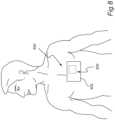
- the present inventive concept also relates to the ADC circuitry being implemented in an integrated circuit device, in a photoplethysmogram detector and/or in a wearable device.
- An integrating ADC is a type of ADC that is configured to convert an unknown analog input signal into a digital representation through using an integrator.
- the integrating ADC may be implemented as a dual-slope ADC, wherein the integrator integrates the analog input signal for ramping an integrator output for a fixed time period (run-up time period). Then, the integrator integrates a reference input signal for returning the integrator output to a threshold (run-down time period).
- the analog input signal may be determined as a function of the reference input signal, the run-up time period and the run-down time period.
- the run-down time period may be measured based on a clock of the ADC, such that use of longer integration times allow for higher resolution of the determination of the analog input signal.
- the integrating ADC may provide a high resolution conversion of the analog input signal, but at a sacrifice of conversion speed.
- a slow conversion speed is also associated with a large power consumption.
- Maghari et al "A Double-Sampled Path-Coupled Single-Loop ⁇ Modulator Using Noise-Shaped Integrating Quantizer", IEEE International Symposium on Circuits and Systems, ISCAS 2010, 30 May-2 June 2010, Paris, France, pages 4005-4008 discloses a single-loop delta-sigma modulator based on path-coupling and double-sampling.
- the modulator employs a noise-shaped integrating quantizer which by itself increases the order of noise shaping by one.
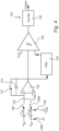
- the timer may be based on a clock of the ADC circuitry. Thanks to the use of the feedforward noise shaping loop, the analog-to-digital conversion can be obtained in few clock periods for utilizing a short time duration. Hence, the ADC circuitry allows relaxation of requirement of clock rate, while enabling the analog-to-digital conversion to be obtained quickly. Thus, the ADC circuitry may perform analog-to-digital conversion with high resolution and low power consumption.
- reduction of quantization error provided by the feedforward noise shaping loop of the ADC circuitry according to the first aspect may be utilized for providing a higher resolution analog-to-digital conversion (with a corresponding conversion time) or a shorter conversion time (with a corresponding resolution).
- the noise shaping capacitor can be reset between samples of the analog input signal. This implies that the ADC circuitry according to the first aspect is not prone to drift of the analog input signal from the threshold.
- the ADC circuitry enables storing of the quantization error on the noise shaping capacitor, such that the integrator may be shut down while the quantization error is stored. This implies that the integrator may be shut down or duty-cycled between processing of samples to save power of the ADC circuitry, while enabling noise shaping to be provided.
- the reference input signal and the threshold may be selected such that a value of the threshold is between values of the analog input signal and the reference input signal. This may be utilized such that the integrator integrating the analog input signal followed by integrating the reference input signal will result in the integrator output being returned towards the threshold by the integrating of the reference input signal.
- a value of the threshold may still be maintained between values of the analog input signal and the reference input signal.
- the feedforward noise shaping loop may form a filter for providing the feedforward noise shaping signal based on the quantization error signal. For instance, in first order noise shaping, a finite impulse response (FIR) filter may be provided, whereas in higher order noise shaping an infinite impulse response (IIR) filter may be provided.
- FIR finite impulse response
- IIR infinite impulse response
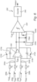
- the feedforward noise shaping loop comprises two sets of noise shaping capacitors for storing quantization error signals from digitizing a first and a second sample of the analog input signal, respectively, wherein the feedforward noise shaping loop forms a second order noise shaping loop using quantization error signals from the first sample and the second sample for changing the threshold of the comparator for digitizing a third sample of the analog input signal following the first and the second samples.
- the quantization error from a particular sample is utilized for providing the feedforward noise shaping signal for two or more following samples.
- plural noise shaping capacitors are needed.
- the quantization error signal for a sample may be stored in each of two noise shaping capacitors of a set.
- the set may comprise two noise shaping capacitors having different capacitances.
- Each of the two noise shaping capacitors of the set may be adapted for providing a weight of the quantization error in dependence of whether the quantization error represents the first sample or the second sample, when digitizing a third sample.
- the quantization error being stored in the set may be utilized for determining the feedforward noise shaping signal for two following samples, without a need to move quantization error information between different capacitors for re-using the quantization error information for the two following samples.
- each set may comprise further noise shaping capacitors such that the quantization error being stored in the set may be utilized for determining the feedforward noise shaping signal for plural following samples.
- the feedforward noise shaping loop further comprises a noise shaping integrator for summing quantization error signals from each of the two sets of noise shaping capacitors to form the feedforward noise shaping signal.
- the feedforward noise shaping loop may form a filter based on the noise shaping integrator. Thanks to summing of quantization error signals from each set of noise shaping capacitors, influence of quantization errors from two previous samples may be used for forming the feedforward noise shaping signal.
- each set of noise shaping capacitors comprises a first noise shaping capacitor having a first capacitance and a second noise shaping capacitor having a second capacitance
- the noise shaping integrator is configured to receive a quantization error signal from the first noise shaping capacitor of the set of noise shaping capacitors representing the second sample and a quantization error signal from the second noise shaping capacitor of the set of noise shaping capacitors representing the first sample.
- each set of noise shaping capacitors comprises a first noise shaping capacitor and a second noise shaping capacitor, which are dedicated for representing the quantization error of the first sample and the second sample, respectively.
- the noise shaping integrator may, for each noise feedforward noise shaping signal to be determined, receive the quantization error from either the first noise shaping capacitor or the second noise shaping capacitor of the set.
- the quantization error may be stored to each of the first noise shaping capacitor and the second noise shaping capacitor.
- the set may thus be used for determining the feedforward noise shaping signal for plural following samples, by the noise shaping integrator using the quantization error signal from the appropriate noise shaping capacitor of the set.
- the second capacitance may be different from the first capacitance such that different weights may be given to the quantization error signal in dependence of whether the quantization error stored in the set represents the first sample or the second sample, when digitizing a third sample.
- the noise shaping capacitors of the sets have a relationship with a feedback capacitor of the noise shaping integrator. Together, the capacitors and the noise shaping integrator form a filter. As long as the filter is stable, the capacitances of the capacitors can have different values.
- the feedforward noise shaping loop is configured to alternatingly store quantization error signals of a sequence of samples in a first set of noise shaping capacitors and in a second set of noise shaping capacitors.
- quantization error signals may be easily stored in the sets without need to move quantization error information between different capacitors for re-using the quantization error information for the two following samples.
- the ADC circuitry further comprises a gain element for amplifying the feedforward noise shaping signal.
- the gain element may be used for further shaping the noise.
- the gain element may be arranged in the comparator but may alternatively be arranged in a separate amplifier of the feedforward noise shaping loop.
- the filter provided by the feedforward noise shaping loop with the gain of the gain element should be designed such that a stable filter is provided.
- the gain of the gain element may be larger than 1 as long as a stable filter is provided, but in some instances the gain of the gain element may be less than 1 in order to obtain a stable filter.
- the input is configured to receive analog input signals in multiple channels, wherein the ADC circuitry comprises multiple feedforward noise shaping loops for storing quantization error signals for the multiple channels.
- the ADC circuitry may thus be used for plural analog input signals, such that the integrator and the comparator may be re-used for the multiple channels.
- Each feedforward noise shaping loop may be dedicated to a specific channel. Hence, quantization error signals may be stored in the feedforward noise shaping loop between different time slots relating to the specific channel in a time-multiplexed input signal.
- the feedforward noise shaping loop 130 may be configured to alternatingly store quantization error signals in the first set of noise shaping capacitors and in the second set of noise shaping capacitors.
- the comparator 120 may be configured to receive the feedforward noise shaping signal, such that the comparator 120 may receive the threshold signal (e.g. V CM ), the integrator output signal INT OUT and the feedforward noise shaping signal V RES_O . With a gain of 2 of the feedforward noise shaping signal, the output of the comparator 120 may thus be determined by: V CM + INT OUT ⁇ 2 V RES _ O .
- the feedforward noise shaping is discussed in detail above for second order noise shaping, it should be realized that higher order noise shaping may be used instead. This may provide better noise shaping.
- the filter of the feedforward noise shaping loop 130 may also be more complex.
- the ADC circuitry 100 is illustrated as receiving the analog input signal and the reference input signal in voltage domain. As shown in Fig. 1 , the analog input signal and the reference input signal may be passed through a respective resistor R 1 and R 2 before being provided at the inverting input of the integrator 102. However, as illustrated in Fig. 3 , the ADC circuitry 100 may alternatively be configured to receive the analog input signal and the reference input signal in the current domain. As shown in Fig. 3 , the analog input signal I IN and the reference input signal I ref may then be provided directly to the inverting input of the integrator 102.
- the ADC circuitry 100 may alternatively be configured to receive the analog input signal and the reference input signal in the charge domain, that is a charge stored on a capacitor C in .
- the analog input signal may be provided in charge domain for instance by detecting the analog input signal from a touch screen or a pressure sensor.
- the switch 106 may select the analog input signal to be provided to the input 104 of the ADC circuitry 100.
- the charge on the capacitor C in holding the analog input signal may then be regarded as a current flowing into the capacitor when the switch 106 is closed.
- a reference charge is stored on capacitor C ref for providing the reference input signal.
- the integrator output will become closer to the threshold and the counter 150 may be incremented, until the integrator output reaches the threshold and the counter 150 is stopped.
- a reference charge may be provided to the capacitor C ref by closing a switch 109 connecting the capacitor C ref to a reference input voltage V ref and the integrator reference signal V CM .
- the charge on the capacitor C ref will be ( V ref - V CM )* C ref , while switches 108a, 108b are open.
- switches 108a, 108b are closed while switch 109 is open, connecting the capacitor C ref between ground and the input 104 of the ADC circuitry 100.
- Another reference charge may then again be provided to the capacitor C ref by switches 108a, 108b being open and switch 109 being closed.
- the ADC circuitry 100 may according to an alternative be configured to selectively receive one of a plurality of reference input signals, V ref , V ref1 , V ref2 , etc., based on switches 108d, 108e, 108f.
- the plurality of reference input signals V ref , V ref1 , V ref2 enables multi-slope analog-to-digital conversion.
- the reference input signals V ref , V ref1 , V ref2 and/or resistances of resistors R 2 , R 3 , R 4 through which the reference input signals are connected to the input of the ADC circuitry 100 may have different values.
- the integrator 102 may be configured to integrate a first reference input signal V ref having a large first value during a first time duration until the integrator output reaches a first threshold and the integrator 102 may further be configured to integrate a second reference input signal V ref1 having a small second value, smaller than the first value, during a second time duration until the integrator 102 reaches a second threshold.
- the integration towards a final threshold may be divided into several periods (or slopes) during which different reference input signals V ref , V ref1 , V ref2 are provided.
- the total time for reaching the final threshold may be reduced compared to the reference input signal having the smallest value being used for the entire time duration.
- the resolution of the determination of the analog input signal may be based on the value of the smallest reference input signal, since the reference input signal having the smallest value may be used during a final period of integrating reference input signals.
- the quantization error is defined based on the reference input signal having the smallest value.
- the plurality of reference input signals V ref , V ref1 , V ref2 may alternatively be adapted for determining digital representations of the analog input signal within different ranges.
- the ADC circuitry 100 may use one reference input signal for determining the digital representation of an analog input signal, such that each instance of determining a digital representation of the analog input signal uses a dual-slope setting of the ADC circuitry 100.
- the reference input signal is selected based on a range within which a value of the analog input signal falls.
- FIG. 6 an ADC circuitry 200 according to an embodiment for analog-to-digital conversion of a fully differential signal will be discussed.
- the ADC circuitry 200 may thus comprise inputs 204a, 204b for receiving differential input signals ( V INN and V INP ) and differential reference input signals ( V refn and V refp ). Switches 206a, 206b and 208a, 208b may be used for controlling whether the differential input signals or the differential output signals are to be provided to the inputs 204a, 204b of the ADC circuitry 200.
- the inputs 204a, 204b may be connected to the integrator 202 of the ADC circuitry 200.
- the integrator 202 may thus switchably receive the analog input signal and the reference input signal on the inputs 204 based on selection by the switches 206a, 206b and 208a, 208b.
- the integrator 202 may be configured to integrate a difference between each of the differential input signals and the integrator reference signal V CM during a first time period (run-up time period). During the first time period, values at differential integrator outputs may be ramped.
- the differential integrator outputs may be stored on respective capacitors 210a, 210b, which may be connected between the integrator output and the respective input of the integrator 202.
- the capacitors 210a, 210b store a charge corresponding to the differential analog input signals and the duration of the first time period.
- the integrator 202 may further be configured to integrate a difference between the reference input signals and the integrator reference signal during a second time period (run-down time period). During the second time period, the value at the integrator output after the first time period, as stored by the capacitors 210a, 210b, will be returned towards a threshold.
- the ADC circuitry 200 further comprises a comparator 220.
- the comparator 220 is configured to compare the integrator outputs to the threshold, in the form of a threshold signal. As indicated in Fig. 6 , the threshold signal may correspond to the integrator reference signal, such that the comparator 220 may receive as input the same signal as the integrator reference signal, V CM , for defining the threshold of the comparator 220.
- the comparator 220 may further receive the integrator outputs as input to the comparator 220.
- the comparator 220 may provide an indication of an end of the run-down time period.
- the ADC circuitry 200 may further comprise two feedforward noise shaping loops 230a, 230b, each associated with one of the integrator outputs.
- the feedforward noise shaping loops 230a, 230b may be configured to store quantization error signals remaining on the integrator outputs when the comparator 220 indicates an end of the run-down time period.
- the quantization errors for each of the differential input signals may be stored in the feedforward noise shaping loops 230a, 230b such that each feedforward noise shaping loop 230a, 230b may provide a feedforward noise shaping signal to the comparator 220 for changing the threshold of the comparator 220.
- the ADC circuitry 200 further comprises a timer 250.
- the timer 250 may be configured to determine a time duration of the run-down time period, which may then be used for determining a digital representation of the differential analog input signals.
- the method may further comprise storing 514, in at least one noise shaping capacitor 131-134 of the feedforward noise shaping loop 130, a quantization error signal that remains on the integrator output, after the second time period.
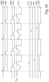
- the signal 614 for controlling the switches 135, 136 may be high for controlling the quantization error signal to be transferred from the integrator output to the first and second capacitors 131, 132 of the first set.
- the method may further comprise generating 516 a feedforward noise shaping signal based on the stored quantization error signal and changing the threshold of the comparator 120 based on the feedforward noise shaping signal for a later sample of the analog input signal.
- the signal 618 for controlling the switches 139 and 142 may be high for controlling the quantization error signals stored in the first capacitor 131 of the first set and in the second capacitor 134 in the second set to be provided to an input of the noise shaping integrator 143.
- a timing diagram using an analog input signal having two channels as for the PPG detector 300 comprising two LEDs 302, 304 is illustrated.
- the additional switch 145 of the feedforward noise shaping loop 130a may be active, as indicated by the signal 622 in Fig. 10 . This implies that the feedforward noise shaping signal is provided to the comparator 120.
- At least some components may be shut down before analog-to-digital conversion of a following sample.
- the LEDs 302, 304, IDACs 312a, 312b, the integrator 102 and the comparator 120 of the ADC circuitry 100 may be shut down. This is illustrated in Fig. 10 , showing that the integrator output 612 goes low during a shut-down period.
- Fig. 10 illustrates a timing diagram using an analog input signal having two channels.
- analog-to-digital conversion of the first sample of the first channel analog-to-digital conversion of a first sample of the second channel is performed.
- the signal 602 for controlling the reset switch 112 is first high to reset the capacitor 110 of the ADC circuitry 100. Then, the signal 608 for controlling the switch 106 may thus be high for a duration defining the first time period to provide the first sample of the second channel to the ADC circuitry 100.
- the second light source 304 and the corresponding IDAC 312b may also be activated during the first time period, as illustrated by the signal 606 in Fig. 10 .
- the integrator output 612 may thus be continuously ramped during the first time period. In the set-up in Fig. 10 , the integrator output 612 may be continuously decreased from a reference voltage level.
- the ADC circuitry 100 comprises a second feedforward noise shaping loop 130b, which stores the quantization error signals relating to the analog-to-digital conversion of the second channel.
- the quantization error signal based on conversion of the first sample of the second channel will be transferred to the noise shaping capacitors of the feedforward noise shaping loop 130b.
- quantization error signals are provided to an input of the noise shaping integrator of the feedforward noise shaping loop 130b.
- the additional switch of the feedforward noise shaping loop 130b may be active.
- analog-to-digital conversion of a second sample of the first channel is performed, in a similar manner as described above for conversion of the first sample of the first channel.
- the feedforward noise shaping signal changes the threshold to which the integrator output 612 is compared.
- the quantization error signal that remains on the integrator output, after the second time period for analog-to-digital conversion of the second sample of the first channel may be stored to the feedforward noise shaping loop.
- the signal 616 for controlling the switches 137, 138 may be high for controlling the quantization error signal to be transferred from the integrator output to the first and second capacitors 133, 134 of the second set.
- the signal 620 for controlling the switches 140 and 141 may then be high for controlling the quantization error signals stored in the second capacitor 132 of the first set and in the first capacitor 133 in the second set to be provided to the input of the noise shaping integrator 143.
Landscapes
- Engineering & Computer Science (AREA)
- Theoretical Computer Science (AREA)
- Analogue/Digital Conversion (AREA)
Claims (15)
- Analog-Digital-Wandler-Schaltung (ADW-Schaltung), umfassend:einen Eingang (104; 204a, 204b), der dazu eingerichtet ist, ein analoges Eingangssignal, das in eine digitale Darstellung umgewandelt werden soll, und ein Referenzeingangssignal zu empfangen;einen Integrator (102; 202), der einen Kondensator (110; 210a, 210b) umfasst, wobei der Integrator (102; 202) dazu eingerichtet ist, zwischen dem Integrieren des analogen Eingangssignals zum Erhöhen eines Integratorausgangs und Zulassen des Aufbaus einer Ladung in dem Kondensator und dem Integrieren des Referenzeingangssignals zum Zurückführen des Integratorausgangs in Richtung einer Schwelle umzuschalten;einen Komparator (120; 220), der dazu eingerichtet ist, den Integratorausgang mit der Schwelle zu vergleichen; undeinen Timer (150; 250), der dazu eingerichtet ist, eine Zeitdauer zu bestimmen, während der das Referenzeingangssignal integriert wird, um den Integratorausgang so zu ändern, dass er die Schwelle erreicht, wobei die Zeitdauer eine digitale Darstellung eines analogen Eingangssignalwertes bereitstellt;dadurch gekennzeichnet, dass die ADW-Schaltung (100; 200) des Weiteren eine Vorkopplungs-Rauschformungsschleife (130; 130a, 130b; 230a, 230b) umfasst, die mindestens einen Rauschformungskondensator (131-134) umfasst, der dazu eingerichtet ist, ein Quantisierungsfehlersignal zu speichern, das, basierend auf dem Digitalisieren einer ersten Abtastung des analogen Eingangssignals, auf dem Integratorausgang verbleibt, wobei der Komparator (120; 220) dazu eingerichtet ist, ein Vorkopplungs-Rauschformungssignal von der Vorkopplungs-Rauschformungsschleife (130; 130a, 130b; 230a, 230b) auf der Grundlage des durch den mindestens einen Rauschformungskondensator (131-134) gespeicherten Quantisierungsfehlersignals zu empfangen, um die Schwelle des Komparators (120; 220) zu ändern, um eine spätere Abtastung des analogen Eingangssignals, die auf die erste Abtastung folgt, zu digitalisieren.
- ADW-Schaltung nach Anspruch 1, wobei die Vorkopplungs-Rauschformungsschleife (130; 130a, 130b; 230a, 230b) zwei Sätze von Rauschformungskondensatoren (131-134) zum Speichern von Quantisierungsfehlersignalen aus dem Digitalisieren einer ersten bzw. einer zweiten Abtastung des analogen Eingangssignals umfasst, wobei die Vorkopplungs-Rauschformungsschleife (130; 130a, 130b; 230a, 230b) eine Rauschformungsschleife zweiter Ordnung bildet, die Quantisierungsfehlersignale von der ersten Abtastung und der zweiten Abtastung verwendet, um die Schwelle des Komparators (120; 220) zu ändern, um eine dritte Abtastung des analogen Eingangssignals, die auf die erste und die zweite Abtastung folgt, zu digitalisieren.
- ADW-Schaltung nach Anspruch 2, wobei die Vorkopplungs-Rauschformungsschleife (130; 130a, 130b; 230a, 230b) des Weiteren einen Rauschformungsintegrator (143) umfasst, um Quantisierungsfehlersignale von jedem der beiden Sätze von Rauschformungskondensatoren (131-134) zu summieren, um das Vorkopplungs-Rauschformungssignal zu bilden.
- ADW-Schaltung nach Anspruch 3, wobei jeder Satz von Rauschformungskondensatoren einen ersten Rauschformungskondensator (131, 133), der eine erste Kapazität besitzt, und einen zweiten Rauschformungskondensator (132, 134), der eine zweite Kapazität besitzt, umfasst, und wobei der Rauschformungsintegrator (143) dazu eingerichtet ist, ein Quantisierungsfehlersignal von dem ersten Rauschformungskondensator (131, 133) des Satzes von Rauschformungskondensatoren, das die zweite Abtastung darstellt, und ein Quantisierungsfehlersignal von dem zweiten Rauschformungskondensator (132, 134) des Satzes von Rauschformungskondensatoren, das die erste Abtastung darstellt, zu empfangen.
- ADW-Schaltung nach einem der Ansprüche 2-4, wobei die Vorkopplungs-Rauschformungsschleife (130; 130a, 130b; 230a, 230b) dazu eingerichtet ist, abwechselnd Quantisierungsfehlersignale einer Sequenz von Abtastungen in einem ersten Satz von Rauschformungskondensatoren (131, 132) und in einem zweiten Satz von Rauschformungskondensatoren (133, 134) zu speichern.
- ADW-Schaltung nach einem der vorangehenden Ansprüche, wobei die ADW-Schaltung (100; 200) des Weiteren ein Verstärkungselement zum Verstärken des Vorkopplungs-Rauschformungssignals umfasst.
- ADW-Schaltung nach einem der vorangehenden Ansprüche, wobei der Eingang dazu eingerichtet ist, analoge Eingangssignale in mehreren Kanälen zu empfangen, wobei die ADW-Schaltung (100; 200) mehrere Vorkopplungs-Rauschformungsschleifen (130a, 130b) zum Speichern von Quantisierungsfehlersignalen für die mehreren Kanäle umfasst.
- ADW-Schaltung nach einem der vorangehenden Ansprüche, wobei der Timer (150; 250) einen Zähler umfasst, der dazu eingerichtet ist, eine digitale Mehrbit-Darstellung des analogen Eingangssignalwertes auszugeben.
- ADW-Schaltung nach einem der vorangehenden Ansprüche, wobei die ADW-Schaltung (100; 200) dazu eingerichtet ist, das analoge Eingangssignal im Strombereich, Spannungsbereich oder Ladungsbereich zu empfangen.
- Integrierte-Schaltkreis-Vorrichtung, umfassend:eine ADW-Schaltung (100; 200) nach einem der vorangehenden Ansprüche, wobei die ADW-Schaltung (100; 200) dazu eingerichtet ist, ein analoges Eingangssignal zu empfangen, um das analoge Eingangssignal in eine digitale Darstellung umzuwandeln; undeine digitale Verarbeitungsschaltung zum digitalen Verarbeiten der digitalen Darstellung des analogen Eingangssignals.
- Photoplethysmogramm-Detektor (PPG-Detektor), umfassend:mindestens eine Lichtquelle (302, 304), die dazu eingerichtet ist, gepulstes Licht zu generieren, um Haut eines Patienten zu beleuchten, um Licht zu generieren, das durch Blutfluss des Patienten moduliert wird;einen Lichtdetektor (305), der dazu eingerichtet ist, das modulierte Licht von dem Patienten zu empfangen, wobei der Lichtdetektor (305) dazu eingerichtet ist, ein analoges Eingangssignal zu generieren; undeine ADW-Schaltung (100; 200) nach einem der Ansprüche 1-9, wobei die ADW-Schaltung (100; 200) dazu eingerichtet ist, das analoge Eingangssignal von dem Lichtdetektor (305) zu empfangen, um das analoge Eingangssignal in eine digitale Darstellung umzuwandeln.
- PPG-Detektor nach Anspruch 11, der des Weiteren eine Gleichstromkompensationsschleife (310) umfasst, die mit dem gepulsten Licht synchronisiert ist, wobei die Gleichstromkompensationsschleife (310) einen Strom-Digital-Analog-Wandler (312a, 312b) umfasst, der mit dem Eingang verbunden ist, um Gleichstromkomponenten von dem analogen Eingangssignal zu subtrahieren, wobei die Gleichstromkompensationsschleife (310) des Weiteren ein Schwellenfilter (316) umfasst, um eine Ausgabe zum Steuern des Strom-Digital-Analog-Wandlers (312a, 312b) auf der Grundlage der digitalen Darstellung des analogen Eingangssignals bereitzustellen.
- PPG-Detektor nach Anspruch 11 oder 12, wobei die mindestens eine Lichtquelle (302, 304) dazu eingerichtet ist, abwechselnd gepulstes Licht von zwei verschiedenen Wellenlängen zu generieren, um die Detektion der Blutsauerstoffsättigung zu ermöglichen, wobei das analoge Eingangssignal zwei abwechselnde Signale umfasst, die sich auf die zwei verschiedenen Wellenlängen beziehen, und wobei die ADW-Schaltung (100; 200) zwei Vorkopplungs-Rauschformungsschleifen (130a, 130b) umfasst, um die Rauschformung der zwei abwechselnden Signale zu handhaben.
- Am Körper tragbare Vorrichtung (400), umfassend:den PPG-Detektor (300) nach einem der Ansprüche 11-13,mindestens einen Träger (402), der dazu eingerichtet ist, an oder um einen Körperteil des Patienten getragen zu werden, wobei der mindestens eine Träger (402) dazu eingerichtet ist, den PPG-Detektor (300) zu tragen.
- Verfahren zur Analog-Digital-Wandlung eines analogen Eingangssignals, umfassend:Auswählen, während eines ersten Zeitraums eine erste Abtastung eines analogen Eingangssignals zu empfangen (502), das an einem Eingang (104; 204a, 204b) einer Analog-Digital-Wandler-Schaltung (100; 200) in eine digitale Darstellung umgewandelt werden soll;Integrieren (504) des analogen Eingangssignals durch einen Integrator (102; 202), der einen Kondensator (110; 210a, 210b) umfasst, während des ersten Zeitraums zum Erhöhen eines Integratorausgangs;Auswählen, während eines zweiten Zeitraums, der auf den ersten Zeitraum folgt, ein Referenzeingangssignal an dem Eingang (104; 204a, 204b) zu empfangen (506);Integrieren (508) des Referenzeingangssignals, um den Integratorausgang in Richtung einer Schwelle zurückzuführen;Vergleichen (510) des Integratorausgangs in einem Komparator (120; 220) mit der Schwelle;Bestimmen (512) einer Zeitdauer des zweiten Zeitraums, während dem das Referenzeingangssignal integriert wird, um den Integratorausgang so zu ändern, dass er die Schwelle erreicht, wobei die Zeitdauer eine digitale Darstellung eines analogen Eingangssignalwertes bereitstellt;gekennzeichnet durch:Speichern (514), in mindestens einem Rauschformungskondensator (131-134) einer Vorkopplungs-Rauschformungsschleife (130; 130a, 130b; 230a, 230b), eines Quantisierungsfehlersignals, das auf dem Integratorausgang verbleibt, nach dem zweiten Zeitraum; undGenerieren (516) eines Vorkopplungs-Rauschformungssignals auf der Grundlage des gespeicherten Quantisierungsfehlersignals und Ändern der Schwelle des Komparators (120; 220) auf der Grundlage des Vorkopplungs-Rauschformungssignals für eine spätere Abtastung des analogen Eingangssignals.
Priority Applications (2)
| Application Number | Priority Date | Filing Date | Title |
|---|---|---|---|
| EP21155525.5A EP4040682B1 (de) | 2021-02-05 | 2021-02-05 | Analog-digital-wandlerschaltung, integrierte schaltvorrichtung, photoplethysmogrammdetektor, wearable-vorrichtung und verfahren zur analog-digital-wandlung |
| US17/590,211 US11689209B2 (en) | 2021-02-05 | 2022-02-01 | Analog-to-digital converter circuitry, an integrated circuit device, a photoplethysmogram detector, a wearable device and a method for analog-to-digital conversion |
Applications Claiming Priority (1)
| Application Number | Priority Date | Filing Date | Title |
|---|---|---|---|
| EP21155525.5A EP4040682B1 (de) | 2021-02-05 | 2021-02-05 | Analog-digital-wandlerschaltung, integrierte schaltvorrichtung, photoplethysmogrammdetektor, wearable-vorrichtung und verfahren zur analog-digital-wandlung |
Publications (2)
| Publication Number | Publication Date |
|---|---|
| EP4040682A1 EP4040682A1 (de) | 2022-08-10 |
| EP4040682B1 true EP4040682B1 (de) | 2025-07-02 |
Family
ID=74556777
Family Applications (1)
| Application Number | Title | Priority Date | Filing Date |
|---|---|---|---|
| EP21155525.5A Active EP4040682B1 (de) | 2021-02-05 | 2021-02-05 | Analog-digital-wandlerschaltung, integrierte schaltvorrichtung, photoplethysmogrammdetektor, wearable-vorrichtung und verfahren zur analog-digital-wandlung |
Country Status (2)
| Country | Link |
|---|---|
| US (1) | US11689209B2 (de) |
| EP (1) | EP4040682B1 (de) |
Family Cites Families (14)
| Publication number | Priority date | Publication date | Assignee | Title |
|---|---|---|---|---|
| WO2001024376A1 (en) * | 1999-09-27 | 2001-04-05 | Parthus Technologies Plc | Method and apparatus for identifying a pre-determined pattern from a received signal via correlation |
| US7142142B2 (en) * | 2004-02-25 | 2006-11-28 | Nelicor Puritan Bennett, Inc. | Multi-bit ADC with sigma-delta modulation |
| DE102006023697B4 (de) * | 2006-05-19 | 2008-02-07 | Infineon Technologies Ag | Verfahren zum Decodieren, Decodierer, Codierer-Decodierer-System und Wandler |
| US7429941B1 (en) * | 2007-05-24 | 2008-09-30 | Infineon Technologies Ag | Stabilization of sigma-delta converters |
| US8045670B2 (en) * | 2007-06-22 | 2011-10-25 | Texas Instruments Incorporated | Interpolative all-digital phase locked loop |
| EP2582050B1 (de) * | 2011-10-13 | 2017-08-09 | OCT Circuit Technologies International Limited | Mehrstufen-Sigma-Delta-Analog-zu-Digital-Wandler mit reduzierten Quantifizierungsstufen |
| US10284213B2 (en) * | 2017-04-21 | 2019-05-07 | Analog Devices, Inc. | Analog-to-digital converter reusing comparator for residue amplifier for noise shaping |
| US10177776B1 (en) * | 2017-08-04 | 2019-01-08 | Mitsubishi Electric Research Laboratories, Inc. | Noise mitigating quantizer for reducing nonlinear distortion in digital signal transmission |
| US10348282B1 (en) * | 2018-07-31 | 2019-07-09 | Cirrus Logic, Inc. | Modulators |
| US10784890B1 (en) * | 2019-05-09 | 2020-09-22 | Dialog Semiconductor B.V. | Signal processor |
| US10763888B1 (en) * | 2019-05-09 | 2020-09-01 | Nxp B.V. | Metastability shaping technique for continuous-time sigma-delta analog-to-digital converters |
| JP2020190642A (ja) * | 2019-05-22 | 2020-11-26 | 旭化成エレクトロニクス株式会社 | Ancシステム |
| EP3817234A1 (de) * | 2019-10-28 | 2021-05-05 | Nxp B.V. | Sigma-delta-modulator, integrierte schaltung und verfahren dafür |
| EP3917012A1 (de) * | 2020-05-26 | 2021-12-01 | Melexis Technologies NV | Sensorschnittstellenschaltung auf basis eines oszillators mit geschlossenem regelkreis |
-
2021
- 2021-02-05 EP EP21155525.5A patent/EP4040682B1/de active Active
-
2022
- 2022-02-01 US US17/590,211 patent/US11689209B2/en active Active
Also Published As
| Publication number | Publication date |
|---|---|
| EP4040682A1 (de) | 2022-08-10 |
| US20220255554A1 (en) | 2022-08-11 |
| US11689209B2 (en) | 2023-06-27 |
Similar Documents
| Publication | Publication Date | Title |
|---|---|---|
| CA2556754C (en) | Multi-bit adc with sigma-delta modulation | |
| Marefat et al. | A 1-V 8.1-$\mu $ W PPG-Recording Front-End With> 92-dB DR Using Light-to-Digital Conversion With Signal-Aware DC Subtraction and Ambient Light Removal | |
| KR101659789B1 (ko) | 근접 검출을 위한 용량성 감지 인터페이스 | |
| US20150145535A1 (en) | Capacitive sensing interface for proximity detection | |
| US8097853B2 (en) | Infrared photocurrent front-end ADC for rain-sensing system with ambient light compensation | |
| Rajesh et al. | 22.4 A 172µW compressive sampling photoplethysmographic readout with embedded direct heart-rate and variability extraction from compressively sampled data | |
| WO2017151648A1 (en) | Bio-sensing device with ambient light cancellation | |
| US6111529A (en) | Accurate gain calibration of analog to digital converters | |
| WO1996013903A1 (en) | Analog-to-digital converter and sensor device comprising such a converter | |
| CN113726328B (zh) | 基于闭环振荡器的传感器接口电路 | |
| Park et al. | A baseline-tracking single-channel I/Q impedance plethysmogram IC for neckband-based blood pressure and cardiovascular monitoring | |
| EP4040682B1 (de) | Analog-digital-wandlerschaltung, integrierte schaltvorrichtung, photoplethysmogrammdetektor, wearable-vorrichtung und verfahren zur analog-digital-wandlung | |
| Yao et al. | A 140 dB-DR light-to-digital converter using current-domain hybrid zoom for baseline cancellation and interference compensation | |
| Li et al. | A 1.8 V 16μA 136.5 dB DR PPG/NIRS recording IC using noise shaping triple slope light to digital converter | |
| Thompson et al. | Pulse oximeter improvement with an ADC-DAC feedback loop and a radial reflectance sensor | |
| Chen et al. | A sub-0.01 phase resolution 6.8-mw fnirs readout circuit employing a mixer-first frequency-domain architecture | |
| Wei et al. | A 153.4 dB-DR PPG recording IC with extended counting and hardware reuse | |
| Saeidi et al. | A Current-to-Digital∆ Σ ADC for Low-Noise High-Precision Applications | |
| CN115644805B (zh) | 一种数字化频域近红外脑功能采集电路 | |
| Zhang et al. | A low-power dynamic-range relaxed analog front end for photoplethysmogram acquisition | |
| Park et al. | A 133.3 dB Dynamic Range Pulse Oximeter Front-End with Low-Noise Area-Efficient Offset Cancellation Current DAC | |
| Pamula et al. | A low-power compressive sampling (CS) photoplethysmogram (PPG) readout with embedded feature extraction | |
| Van Helleputte et al. | Advances in biomedical sensor systems for wearable health | |
| JPH0386152A (ja) | オキシメーター | |
| KR20210107499A (ko) | 아날로그 전단 회로 및 이를 포함하는 산소 포화도 측정기 |
Legal Events
| Date | Code | Title | Description |
|---|---|---|---|
| PUAI | Public reference made under article 153(3) epc to a published international application that has entered the european phase |
Free format text: ORIGINAL CODE: 0009012 |
|
| STAA | Information on the status of an ep patent application or granted ep patent |
Free format text: STATUS: THE APPLICATION HAS BEEN PUBLISHED |
|
| AK | Designated contracting states |
Kind code of ref document: A1 Designated state(s): AL AT BE BG CH CY CZ DE DK EE ES FI FR GB GR HR HU IE IS IT LI LT LU LV MC MK MT NL NO PL PT RO RS SE SI SK SM TR |
|
| STAA | Information on the status of an ep patent application or granted ep patent |
Free format text: STATUS: REQUEST FOR EXAMINATION WAS MADE |
|
| 17P | Request for examination filed |
Effective date: 20230210 |
|
| RBV | Designated contracting states (corrected) |
Designated state(s): AL AT BE BG CH CY CZ DE DK EE ES FI FR GB GR HR HU IE IS IT LI LT LU LV MC MK MT NL NO PL PT RO RS SE SI SK SM TR |
|
| GRAP | Despatch of communication of intention to grant a patent |
Free format text: ORIGINAL CODE: EPIDOSNIGR1 |
|
| STAA | Information on the status of an ep patent application or granted ep patent |
Free format text: STATUS: GRANT OF PATENT IS INTENDED |
|
| RIC1 | Information provided on ipc code assigned before grant |
Ipc: H03M 1/06 20060101ALN20250115BHEP Ipc: H03M 1/12 20060101ALN20250115BHEP Ipc: H03M 1/54 20060101ALI20250115BHEP Ipc: H03M 1/52 20060101ALI20250115BHEP Ipc: H03M 1/08 20060101AFI20250115BHEP |
|
| RIC1 | Information provided on ipc code assigned before grant |
Ipc: H03M 1/06 20060101ALN20250127BHEP Ipc: H03M 1/12 20060101ALN20250127BHEP Ipc: H03M 1/54 20060101ALI20250127BHEP Ipc: H03M 1/52 20060101ALI20250127BHEP Ipc: H03M 1/08 20060101AFI20250127BHEP |
|
| INTG | Intention to grant announced |
Effective date: 20250211 |
|
| RIC1 | Information provided on ipc code assigned before grant |
Ipc: H03M 1/06 20060101ALN20250203BHEP Ipc: H03M 1/12 20060101ALN20250203BHEP Ipc: H03M 1/54 20060101ALI20250203BHEP Ipc: H03M 1/52 20060101ALI20250203BHEP Ipc: H03M 1/08 20060101AFI20250203BHEP |
|
| P01 | Opt-out of the competence of the unified patent court (upc) registered |
Free format text: CASE NUMBER: APP_14889/2025 Effective date: 20250327 |
|
| GRAS | Grant fee paid |
Free format text: ORIGINAL CODE: EPIDOSNIGR3 |
|
| GRAA | (expected) grant |
Free format text: ORIGINAL CODE: 0009210 |
|
| STAA | Information on the status of an ep patent application or granted ep patent |
Free format text: STATUS: THE PATENT HAS BEEN GRANTED |
|
| AK | Designated contracting states |
Kind code of ref document: B1 Designated state(s): AL AT BE BG CH CY CZ DE DK EE ES FI FR GB GR HR HU IE IS IT LI LT LU LV MC MK MT NL NO PL PT RO RS SE SI SK SM TR |
|
| REG | Reference to a national code |
Ref country code: GB Ref legal event code: FG4D |
|
| REG | Reference to a national code |
Ref country code: CH Ref legal event code: EP |
|
| REG | Reference to a national code |
Ref country code: DE Ref legal event code: R096 Ref document number: 602021033154 Country of ref document: DE |
|
| REG | Reference to a national code |
Ref country code: IE Ref legal event code: FG4D |
|
| REG | Reference to a national code |
Ref country code: NL Ref legal event code: MP Effective date: 20250702 |
|
| PG25 | Lapsed in a contracting state [announced via postgrant information from national office to epo] |
Ref country code: PT Free format text: LAPSE BECAUSE OF FAILURE TO SUBMIT A TRANSLATION OF THE DESCRIPTION OR TO PAY THE FEE WITHIN THE PRESCRIBED TIME-LIMIT Effective date: 20251103 |
|
| PG25 | Lapsed in a contracting state [announced via postgrant information from national office to epo] |
Ref country code: NL Free format text: LAPSE BECAUSE OF FAILURE TO SUBMIT A TRANSLATION OF THE DESCRIPTION OR TO PAY THE FEE WITHIN THE PRESCRIBED TIME-LIMIT Effective date: 20250702 |
|
| REG | Reference to a national code |
Ref country code: AT Ref legal event code: MK05 Ref document number: 1810454 Country of ref document: AT Kind code of ref document: T Effective date: 20250702 |
|
| PG25 | Lapsed in a contracting state [announced via postgrant information from national office to epo] |
Ref country code: IS Free format text: LAPSE BECAUSE OF FAILURE TO SUBMIT A TRANSLATION OF THE DESCRIPTION OR TO PAY THE FEE WITHIN THE PRESCRIBED TIME-LIMIT Effective date: 20251102 |
|
| PG25 | Lapsed in a contracting state [announced via postgrant information from national office to epo] |
Ref country code: NO Free format text: LAPSE BECAUSE OF FAILURE TO SUBMIT A TRANSLATION OF THE DESCRIPTION OR TO PAY THE FEE WITHIN THE PRESCRIBED TIME-LIMIT Effective date: 20251002 |
|
| REG | Reference to a national code |
Ref country code: LT Ref legal event code: MG9D |
|
| PG25 | Lapsed in a contracting state [announced via postgrant information from national office to epo] |
Ref country code: AT Free format text: LAPSE BECAUSE OF FAILURE TO SUBMIT A TRANSLATION OF THE DESCRIPTION OR TO PAY THE FEE WITHIN THE PRESCRIBED TIME-LIMIT Effective date: 20250702 |
|
| PG25 | Lapsed in a contracting state [announced via postgrant information from national office to epo] |
Ref country code: FI Free format text: LAPSE BECAUSE OF FAILURE TO SUBMIT A TRANSLATION OF THE DESCRIPTION OR TO PAY THE FEE WITHIN THE PRESCRIBED TIME-LIMIT Effective date: 20250702 |
|
| PG25 | Lapsed in a contracting state [announced via postgrant information from national office to epo] |
Ref country code: HR Free format text: LAPSE BECAUSE OF FAILURE TO SUBMIT A TRANSLATION OF THE DESCRIPTION OR TO PAY THE FEE WITHIN THE PRESCRIBED TIME-LIMIT Effective date: 20250702 |
|
| PG25 | Lapsed in a contracting state [announced via postgrant information from national office to epo] |
Ref country code: GR Free format text: LAPSE BECAUSE OF FAILURE TO SUBMIT A TRANSLATION OF THE DESCRIPTION OR TO PAY THE FEE WITHIN THE PRESCRIBED TIME-LIMIT Effective date: 20251003 |
|
| PG25 | Lapsed in a contracting state [announced via postgrant information from national office to epo] |
Ref country code: SE Free format text: LAPSE BECAUSE OF FAILURE TO SUBMIT A TRANSLATION OF THE DESCRIPTION OR TO PAY THE FEE WITHIN THE PRESCRIBED TIME-LIMIT Effective date: 20250702 Ref country code: CZ Free format text: LAPSE BECAUSE OF FAILURE TO SUBMIT A TRANSLATION OF THE DESCRIPTION OR TO PAY THE FEE WITHIN THE PRESCRIBED TIME-LIMIT Effective date: 20250702 |
|
| PG25 | Lapsed in a contracting state [announced via postgrant information from national office to epo] |
Ref country code: LV Free format text: LAPSE BECAUSE OF FAILURE TO SUBMIT A TRANSLATION OF THE DESCRIPTION OR TO PAY THE FEE WITHIN THE PRESCRIBED TIME-LIMIT Effective date: 20250702 |
|
| PG25 | Lapsed in a contracting state [announced via postgrant information from national office to epo] |
Ref country code: PL Free format text: LAPSE BECAUSE OF FAILURE TO SUBMIT A TRANSLATION OF THE DESCRIPTION OR TO PAY THE FEE WITHIN THE PRESCRIBED TIME-LIMIT Effective date: 20250702 Ref country code: BG Free format text: LAPSE BECAUSE OF FAILURE TO SUBMIT A TRANSLATION OF THE DESCRIPTION OR TO PAY THE FEE WITHIN THE PRESCRIBED TIME-LIMIT Effective date: 20250702 |
|
| PG25 | Lapsed in a contracting state [announced via postgrant information from national office to epo] |
Ref country code: RS Free format text: LAPSE BECAUSE OF FAILURE TO SUBMIT A TRANSLATION OF THE DESCRIPTION OR TO PAY THE FEE WITHIN THE PRESCRIBED TIME-LIMIT Effective date: 20251002 |
|
| PG25 | Lapsed in a contracting state [announced via postgrant information from national office to epo] |
Ref country code: ES Free format text: LAPSE BECAUSE OF FAILURE TO SUBMIT A TRANSLATION OF THE DESCRIPTION OR TO PAY THE FEE WITHIN THE PRESCRIBED TIME-LIMIT Effective date: 20250702 |
|
| PG25 | Lapsed in a contracting state [announced via postgrant information from national office to epo] |
Ref country code: SM Free format text: LAPSE BECAUSE OF FAILURE TO SUBMIT A TRANSLATION OF THE DESCRIPTION OR TO PAY THE FEE WITHIN THE PRESCRIBED TIME-LIMIT Effective date: 20250702 |
|
| PG25 | Lapsed in a contracting state [announced via postgrant information from national office to epo] |
Ref country code: DK Free format text: LAPSE BECAUSE OF FAILURE TO SUBMIT A TRANSLATION OF THE DESCRIPTION OR TO PAY THE FEE WITHIN THE PRESCRIBED TIME-LIMIT Effective date: 20250702 |
|
| PGFP | Annual fee paid to national office [announced via postgrant information from national office to epo] |
Ref country code: DE Payment date: 20260121 Year of fee payment: 6 |
|
| PG25 | Lapsed in a contracting state [announced via postgrant information from national office to epo] |
Ref country code: IT Free format text: LAPSE BECAUSE OF FAILURE TO SUBMIT A TRANSLATION OF THE DESCRIPTION OR TO PAY THE FEE WITHIN THE PRESCRIBED TIME-LIMIT Effective date: 20250702 |
|
| PG25 | Lapsed in a contracting state [announced via postgrant information from national office to epo] |
Ref country code: SK Free format text: LAPSE BECAUSE OF FAILURE TO SUBMIT A TRANSLATION OF THE DESCRIPTION OR TO PAY THE FEE WITHIN THE PRESCRIBED TIME-LIMIT Effective date: 20250702 Ref country code: EE Free format text: LAPSE BECAUSE OF FAILURE TO SUBMIT A TRANSLATION OF THE DESCRIPTION OR TO PAY THE FEE WITHIN THE PRESCRIBED TIME-LIMIT Effective date: 20250702 |