EP4040517A1 - Optical waveguide package and light-emitting device - Google Patents
Optical waveguide package and light-emitting device Download PDFInfo
- Publication number
- EP4040517A1 EP4040517A1 EP20872805.5A EP20872805A EP4040517A1 EP 4040517 A1 EP4040517 A1 EP 4040517A1 EP 20872805 A EP20872805 A EP 20872805A EP 4040517 A1 EP4040517 A1 EP 4040517A1
- Authority
- EP
- European Patent Office
- Prior art keywords
- light
- cladding
- lid
- optical waveguide
- emitting device
- Prior art date
- Legal status (The legal status is an assumption and is not a legal conclusion. Google has not performed a legal analysis and makes no representation as to the accuracy of the status listed.)
- Pending
Links
Images




Classifications
-
- H—ELECTRICITY
- H01—ELECTRIC ELEMENTS
- H01S—DEVICES USING THE PROCESS OF LIGHT AMPLIFICATION BY STIMULATED EMISSION OF RADIATION [LASER] TO AMPLIFY OR GENERATE LIGHT; DEVICES USING STIMULATED EMISSION OF ELECTROMAGNETIC RADIATION IN WAVE RANGES OTHER THAN OPTICAL
- H01S5/00—Semiconductor lasers
- H01S5/02—Structural details or components not essential to laser action
- H01S5/022—Mountings; Housings
- H01S5/023—Mount members, e.g. sub-mount members
- H01S5/02315—Support members, e.g. bases or carriers
-
- G—PHYSICS
- G02—OPTICS
- G02B—OPTICAL ELEMENTS, SYSTEMS OR APPARATUS
- G02B6/00—Light guides; Structural details of arrangements comprising light guides and other optical elements, e.g. couplings
- G02B6/24—Coupling light guides
- G02B6/42—Coupling light guides with opto-electronic elements
- G02B6/4201—Packages, e.g. shape, construction, internal or external details
- G02B6/4256—Details of housings
- G02B6/4257—Details of housings having a supporting carrier or a mounting substrate or a mounting plate
-
- G—PHYSICS
- G02—OPTICS
- G02B—OPTICAL ELEMENTS, SYSTEMS OR APPARATUS
- G02B6/00—Light guides; Structural details of arrangements comprising light guides and other optical elements, e.g. couplings
- G02B6/24—Coupling light guides
- G02B6/42—Coupling light guides with opto-electronic elements
-
- G—PHYSICS
- G02—OPTICS
- G02B—OPTICAL ELEMENTS, SYSTEMS OR APPARATUS
- G02B6/00—Light guides; Structural details of arrangements comprising light guides and other optical elements, e.g. couplings
- G02B6/24—Coupling light guides
- G02B6/42—Coupling light guides with opto-electronic elements
- G02B6/4201—Packages, e.g. shape, construction, internal or external details
- G02B6/4251—Sealed packages
-
- G—PHYSICS
- G02—OPTICS
- G02B—OPTICAL ELEMENTS, SYSTEMS OR APPARATUS
- G02B6/00—Light guides; Structural details of arrangements comprising light guides and other optical elements, e.g. couplings
- G02B6/24—Coupling light guides
- G02B6/42—Coupling light guides with opto-electronic elements
- G02B6/4201—Packages, e.g. shape, construction, internal or external details
- G02B6/4266—Thermal aspects, temperature control or temperature monitoring
- G02B6/4268—Cooling
-
- H—ELECTRICITY
- H01—ELECTRIC ELEMENTS
- H01S—DEVICES USING THE PROCESS OF LIGHT AMPLIFICATION BY STIMULATED EMISSION OF RADIATION [LASER] TO AMPLIFY OR GENERATE LIGHT; DEVICES USING STIMULATED EMISSION OF ELECTROMAGNETIC RADIATION IN WAVE RANGES OTHER THAN OPTICAL
- H01S5/00—Semiconductor lasers
- H01S5/02—Structural details or components not essential to laser action
- H01S5/022—Mountings; Housings
- H01S5/0233—Mounting configuration of laser chips
- H01S5/02345—Wire-bonding
-
- H—ELECTRICITY
- H10—SEMICONDUCTOR DEVICES; ELECTRIC SOLID-STATE DEVICES NOT OTHERWISE PROVIDED FOR
- H10H—INORGANIC LIGHT-EMITTING SEMICONDUCTOR DEVICES HAVING POTENTIAL BARRIERS
- H10H20/00—Individual inorganic light-emitting semiconductor devices having potential barriers, e.g. light-emitting diodes [LED]
- H10H20/80—Constructional details
- H10H20/85—Packages
- H10H20/852—Encapsulations
- H10H20/853—Encapsulations characterised by their shape
-
- H—ELECTRICITY
- H10—SEMICONDUCTOR DEVICES; ELECTRIC SOLID-STATE DEVICES NOT OTHERWISE PROVIDED FOR
- H10H—INORGANIC LIGHT-EMITTING SEMICONDUCTOR DEVICES HAVING POTENTIAL BARRIERS
- H10H20/00—Individual inorganic light-emitting semiconductor devices having potential barriers, e.g. light-emitting diodes [LED]
- H10H20/80—Constructional details
- H10H20/85—Packages
- H10H20/857—Interconnections, e.g. lead-frames, bond wires or solder balls
-
- H—ELECTRICITY
- H01—ELECTRIC ELEMENTS
- H01S—DEVICES USING THE PROCESS OF LIGHT AMPLIFICATION BY STIMULATED EMISSION OF RADIATION [LASER] TO AMPLIFY OR GENERATE LIGHT; DEVICES USING STIMULATED EMISSION OF ELECTROMAGNETIC RADIATION IN WAVE RANGES OTHER THAN OPTICAL
- H01S5/00—Semiconductor lasers
- H01S5/02—Structural details or components not essential to laser action
- H01S5/022—Mountings; Housings
- H01S5/02208—Mountings; Housings characterised by the shape of the housings
-
- H—ELECTRICITY
- H01—ELECTRIC ELEMENTS
- H01S—DEVICES USING THE PROCESS OF LIGHT AMPLIFICATION BY STIMULATED EMISSION OF RADIATION [LASER] TO AMPLIFY OR GENERATE LIGHT; DEVICES USING STIMULATED EMISSION OF ELECTROMAGNETIC RADIATION IN WAVE RANGES OTHER THAN OPTICAL
- H01S5/00—Semiconductor lasers
- H01S5/40—Arrangement of two or more semiconductor lasers, not provided for in groups H01S5/02 - H01S5/30
- H01S5/4025—Array arrangements, e.g. constituted by discrete laser diodes or laser bar
- H01S5/4087—Array arrangements, e.g. constituted by discrete laser diodes or laser bar emitting more than one wavelength
- H01S5/4093—Red, green and blue [RGB] generated directly by laser action or by a combination of laser action with nonlinear frequency conversion
Definitions
- the present disclosure relates to an optical waveguide package and a light-emitting device.
- a known optical waveguide package and a light-emitting device including the optical waveguide package are described in, for example, Patent Literature 1.
- the known structure includes a substrate, a cladding layer on the substrate, a laser diode (LD) and a photodiode (PD) in etched portions in the cladding layer, and a lid covering the LD and the PD.
- LD laser diode
- PD photodiode
- Patent Literature 1 Japanese Patent No. 3324936
- An optical waveguide package includes a substrate, a cladding on the substrate, a core in the cladding, a lid, and a metal member.
- the cladding includes a first surface facing the substrate, a second surface opposite to the first surface, and an element-receiving area being open in the second surface.
- the core extends from the element-receiving area.
- the lid covers the element-receiving area.
- the metal member is located between the cladding and the lid.
- a light-emitting device includes the above optical waveguide package, a light-emitting element in the element-receiving area, and a lens on an optical path of light to be emitted from the core.
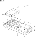
- FIG. 1 is an exploded perspective view of a light-emitting device including an optical waveguide package according to an embodiment of the present disclosure.
- FIG. 2 is a perspective view of the light-emitting device in FIG. 1 without showing a lid.
- FIG. 3 is a cross-sectional view of the light-emitting device taken along the section line in FIG. 2 .
- FIG. 4 is a plan view of the light-emitting device.
- FIG. 5 is an enlarged plan view of an element-receiving area and its adjacent area in the optical waveguide package.
- An optical waveguide package 100 includes a substrate 1, an optical waveguide layer 5, a lid 11, and a metal member 12.
- the optical waveguide layer 5 is on an upper surface 2 of the substrate 1 and includes a cladding 3 and a core 4 in the cladding 3.
- the cladding 3 has a first surface 3a facing the substrate 1, a second surface 3b opposite to the first surface 3a, and an element-receiving area 9 that is open in the second surface 3b.
- the lid 11 covers the element-receiving area 9.
- the metal member 12 is between the cladding 3 and the lid 11.
- the optical waveguide package 100 includes multiple (three in the present embodiment) element-receiving areas 9 each accommodating a light-emitting element 10.
- the optical waveguide package 100, the light-emitting elements 10 in the element-receiving areas 9, and a lens 45 on the optical path of the light emitted from the core 4 form a light-emitting device 200.
- the light-emitting elements 10 may be laser diodes.
- the optical waveguide package 100 according to the present embodiment accommodates three light-emitting elements 10.
- the light-emitting elements 10 emit light with respective colors, for example, red (R) light, green (G) light, or blue (B) light.
- the optical waveguide layer 5 includes the core 4 and the cladding 3 integral with each other.
- the substrate 1 may include multiple dielectric layers stacked on one another.
- the substrate 1 may be a ceramic wiring board including dielectric layers formed from a ceramic material.
- the ceramic material used for the ceramic wiring board include sintered aluminum oxide, sintered mullite, sintered silicon carbide, sintered aluminum nitride, and sintered glass ceramic.
- the dielectric layers include conductors such as connection pads, internal wiring conductors, and external connection terminals for electrical connection between the light-emitting and light-receiving elements and an external circuit.
- the substrate 1 may be an organic wiring board including dielectric layers formed from an organic material.
- the organic wiring board may be a printed wiring board, a build-up wiring board, or a flexible wiring board.
- Examples of the organic material used for the organic wiring board include an epoxy resin, a polyimide resin, a polyester resin, an acrylic resin, a phenolic resin, and a fluororesin.
- the optical waveguide layer 5 may be glass such as quartz, or a resin.
- both the core 4 and the cladding 3 may be glass or a resin.
- one of the core 4 and the cladding 3 may be glass and the other may be a resin.
- the core 4 has a higher refractive index than the cladding 3. The difference in the refractive index causes total internal reflection of light. More specifically, a material with a higher refractive index is used to form a path, which is then surrounded by a material with a lower refractive index. This structure confines light in the core 4 with the higher refractive index.
- the core 4 extends from the element-receiving areas 9 to allow light emitted from the light-emitting elements 10 on three element mounting portions 8 to be combined and reach the lens 45 in the present embodiment.
- the core 4 in the present embodiment has three incident end faces 4a, 4b, and 4c corresponding to the respective element mounting portions 8, and one emission end face 42.
- the core 4 defines a merging path including branching paths 41a, 41b, and 41c, a merging portion 43, and a joined path 44 between the incident end faces 4a, 4b, and 4c and the emission end face 42.
- the branching paths 41a, 41b, and 41c respectively have the incident end faces 4a, 4b, and 4c at one end.
- the merging portion 43 merges the branching paths 41a, 41b, and 41c together.
- the joined path 44 has the emission end face 42 at one end.
- Red (R) light, green (G) light, and blue (B) light emitted from the respective light-emitting elements 10 enter the respective branching paths 41a, 41b, and 41c through the incident end faces 4a, 4b, and 4c and pass through the merging portion 43 and the joined path 44 to the lens 45, through which the light is condensed and emitted.
- the lens 45 is, for example, a plano-convex lens with a flat incident surface facing the core 4 and a convex emission surface.
- the optical waveguide layer 5, the light-emitting elements 10, and the lens 45 are assembled together to have the branching paths 41a, 41b, and 41c each with its optical axis aligned with the center of the light emitter of the corresponding light-emitting element 10, and to have the joined path 44 and the lens 45 with their optical axes aligned with each other.
- the cladding 3 has through-holes 30 in the second surface 3b. In other words, the cladding 3 also has openings in the first surface 3a.
- the upper surface 2 of the substrate 1 and the through-holes 30 define compartments 31 for the light-emitting elements 10. Each compartment 31 has the element mounting portion 8 on the bottom.
- the element mounting portions 8 are used to join the light-emitting elements 10 to the upper surface 2 of the substrate 1.
- the element mounting portions 8 may include metal members such as metallized layers located on the upper surface 2 of the substrate.
- the metal members in the element mounting portions 8 are joined to the light-emitting elements 10 with a die bonding material such as a brazing material or an adhesive.
- the metal members in the element mounting portions 8 are connected to external wiring members 15.
- the light-emitting elements 10 include electrodes on the lower surfaces electrically connectable to the metal members in the element mounting portions 8 and further to, for example, an external power circuit through the external wiring members 15.
- the external wiring members 15 extend across inside and outside the compartments 31.
- the light-emitting elements 10 include electrodes on the upper surfaces that may be electrically connected to the external wiring members 15 (not connected to the metal members in the element mounting portions 8) with, for example, bonding wires (not shown).
- the lid 11 for covering the element-receiving areas 9 is on the second surface 3b of the cladding 3.
- the metal member 12 surrounds the element-receiving areas 9 between the lid 11 and the cladding 3 to improve airtightness in the compartments 31 accommodating the light-emitting elements 10.
- the metal member 12 is, for example, in a continuous loop and surrounds the through-holes 30 in a plan view.
- the cladding 3 and the second surface 3b joined together with the metal member 12 allow the compartments 31 to be more airtight than the cladding 3 and the lid 11 joined together with, for example, a resin adhesive.
- the lid 11 may be formed from a glass material such as quartz, borosilicate, or sapphire.
- the lid 11 may have a recess 11a.
- the lid 11 has the recess 11a facing the element-receiving areas 9.
- the light-emitting elements 10 extend from the element-receiving areas 9 into the recess 11a.
- the light-emitting elements 10 received in the element-receiving areas 9 may have a greater height than the cladding 3, or in other words, the light-emitting elements 10 may protrude from the second surface 3b of the cladding 3.
- the lid 11 receives the protruding areas in the recess 11a and can thus be joined to the cladding 3 with the metal member 12 in between. In other words, the lid 11 with the above structure allows the cladding 3 to be thinner.
- the lid 11 is located on a first region 3b1 of the cladding 3 and thus reduces the height of the light-emitting device 200.
- the metal member 12 is located on the second surface 3b of the cladding 3.
- the metal member 12 is formed from Ti, Ni, Au, Pt, or Cr, or two or more of these metals, and is fixed on the second surface 3b of the cladding 3 by vapor deposition, sputtering, ion plating, or plating.
- the lid 11 is joined to the metal member 12 by, for example, thermal curing or laser welding using a bond, such as Au-Sn or Sn-Ag-Cu solder, a metal nanoparticle paste of Ag or Cu, or a glass paste.
- the metal member 12 may be located on the lid 11, rather than on the cladding 3, in an area facing the cladding 3.
- the metal member 12 is formed from Ti, Ni, Au, Pt, or Cr, or two or more of these metals, and is fixed on the lid 11 by vapor deposition, sputtering, ion plating, or plating.
- the cladding 3 is joined to the metal member 12 by, for example, thermal curing or laser welding using a bond, such as Au-Sn or Sn-Ag-Cu solder, a metal nanoparticle paste of Ag or Cu, or a glass paste.
- the metal member 12 may be located on both the cladding 3 and the lid 11.
- the metal member 12 on the cladding 3 is joined to the metal member 12 on the lid 11 by, for example, thermal curing or laser welding using a bond, such as Au-Sn or Sn-Ag-Cu solder, a metal nanoparticle paste of Ag or Cu, or a glass paste.
- the second surface 3b of the cladding 3 includes the first region 3b1 surrounding the element-receiving areas 9 in a plan view and a second region 3b2 other than the first region 3b 1.
- the lid 11 is located only on the first region 3b1. This structure allows the second region 3b2 to be at a lower height than with the lid 11 extending over the entire second surface 3b including the second region 3b2.
- the lid 11 may extend over the entire second surface 3b to protect the second surface 3b of the cladding 3.
- One compartment 31 may include multiple element mounting portions 8. In other words, such multiple element mounting portions 8 are located in one of the through-holes 30 in a plan view.
- one compartment 31 includes multiple element mounting portions 8 and partitions 32 each between the element-receiving areas 9.
- the compartment 31, separated by the partitions 32 has spaces defined for the respective element mounting portions 8 to receive the light-emitting elements 10.
- the multiple element-receiving areas 9 are separated by the partitions 32 for receiving the light-emitting elements 10. Light emitted from one light-emitting element 10 may be partially reflected without entering the incident end face 4a of the core 4, possibly causing stray light in the compartment 31. This may affect the other light-emitting elements 10.
- the partitions 32 can reduce the effects of such stray light.
- the cladding 3 may receive thermal stress upon being heated when, for example, the light-emitting elements 10 are operating, the lid 11 is joined to the cladding 3, or the light-emitting elements 10 are mounted on the element mounting portions 8.
- the thermal stress may cause deformation of the element-receiving areas 9 and their adjacent areas in the cladding 3, possibly causing cracks, peeling of the metal member 12, or peeling of the cladding from the substrate 1. This may also reduce the airtightness.
- the partitions 32 can increase the heat transfer paths to dissipate heat, reduce deformation of the cladding 3 under thermal stress, and lower the likelihood of airtightness reduction.
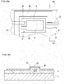
- FIG. 6A is a plan view of an optical waveguide package according to another embodiment of the present disclosure.
- FIG. 6B is a cross-sectional view of the optical waveguide package taken along the section line in FIG. 6A .
- the cladding 3 includes a protrusion 33 above the core 4.
- the protrusion 33 protrudes from the second surface 3b of the cladding 3.
- the protrusion 33 is above the core 4 (adjacent to the second surface 3b).
- the core 4 may be at least partially within the protrusion 33.
- the protrusion 33 may be in, for example, the first region 3b1 and the second region 3b2 and may extend along the core 4.
- the metal member 12 extends along the surface of the protrusion 33.
- the bond between the lid 11 and the metal member 12 is thinner on the protrusion 33 than on the other area.
- the protrusion 33 has a smaller amount of bond on its surface than the other area. Heat applied to join the lid 11 transfers through the bond and the metal member 12 to the cladding 3.
- the protrusion 33 having the smaller amount of bond reduces heat transferring to the core 4 below the protrusion 33, thus lowering the likelihood of deteriorating optical transmission characteristics under heat.
- FIG. 7A is a plan view of a light-emitting device according to another embodiment of the present disclosure.
- FIG. 7B is a cross-sectional view of the light-emitting device taken along the section line in FIG. 7A .
- the components corresponding to those in the above embodiments are given the same reference numerals and will not be described repeatedly.
- the cladding 3 includes, in the first region 3b1, a step 34 fitted with the lid 11. This structure increases the strength for joining the lid 11 to the cladding 3 with the metal member 12 in between.
- the step 34 may have any shape to fit to the lid 11.
- the step 34 has a step surface 34a defined by an inner portion of the first region 3b1 (an edge of the through-hole 30) one step lower and closer to the first surface 3a of the cladding 3.
- the lid 11 may have any shape to fit to the step 34.
- the lid 11 may include a step shaped in correspondence with the step 34.
- the metal member 12 may be located entirely or partially on the step 34.
- the metal member 12 may be on an outer portion of the first region 3b1 (a portion surrounding the step surface 34a) without being located on the step surface 34a.
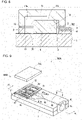
- FIG. 8 is a cross-sectional view of a light-emitting device according to another embodiment of the present disclosure.
- the lid 11 includes a contact portion 11b in contact with the light-emitting elements 10.
- the contact portion 11b protrudes outward from the surface of the lid 11 facing the element-receiving areas 9.
- the lid 11 has a recess 11a receiving the contact portion 11b.
- the lid 11 joined to the cladding 3 with the metal member 12 in between may have the contact portion 11b in contact with the light-emitting elements 10.
- the operating light-emitting elements 10 For the lid 11 with no contact portion 11b, the operating light-emitting elements 10 generate heat that mainly transfers through the element mounting portions 8 to the substrate 1 for dissipation. For the lid 11 with the contact portion 11b, the operating light-emitting elements 10 generate heat that transfers through the element mounting portions 8 to the substrate 1 and also transfers through the contact portion 11b to the lid 11 for dissipation, for example, from the surface of the lid 11. This reduces the effects of heat from the operating light-emitting elements 10.
- FIG. 9 is an exploded perspective view of a light-emitting device 200A according to still another embodiment of the present disclosure.
- FIG. 10 is a perspective view of the light-emitting device 200A in FIG. 9 without showing a lid 11A.
- FIG. 11 is a cross-sectional view of the light-emitting device 200A taken along the section line in FIG. 9 .
- the components corresponding to those in the above embodiments are given the same reference numerals and will not be described repeatedly.
- the light-emitting elements 10 include upper portions protruding from the cladding 3. The protruding portions are received in the recess 11a in the lid 11.
- an optical waveguide package 100A includes a cladding 3 thicker than the light-emitting elements 10.
- the compartments 31 each accommodate the entire light-emitting element 10 and are covered with a plate-like lid 11A. This structure allows the lid 11A to have no recess 11a and thus simplifies the lid 11A.
- a light-emitting device 200 may include a thermistor.
- the thermistor may be located to detect the temperature of the optical waveguide layer 5, or may be located in each compartment 31 to detect the temperature of the light-emitting element 10, or may be located on each external wiring member 15 outside the compartments 31.
- the light-emitting device 200 may also include a light-receiving element in each compartment 31.
- a light-receiving element is located opposite to the incident end face 4a from a light-emitting element 10.
- the light-emitting element 10 emits light toward the incident end face 4a and simultaneously emits the same light in the opposite direction.
- the light-receiving element can receive and observe the light from the light-emitting element 10 to control the output from the light-emitting element 10.
- the light-emitting elements 10 are not limited to light-emitting diodes (LEDs) but may be, for example, laser diodes (LDs) or vertical cavity surface emitting lasers (VCSELs).
- LEDs light-emitting diodes
- LDs laser diodes
- VCSELs vertical cavity surface emitting lasers
Landscapes
- Physics & Mathematics (AREA)
- General Physics & Mathematics (AREA)
- Optics & Photonics (AREA)
- Condensed Matter Physics & Semiconductors (AREA)
- Electromagnetism (AREA)
- Optical Integrated Circuits (AREA)
- Optical Couplings Of Light Guides (AREA)
- Semiconductor Lasers (AREA)
Abstract
Description
- The present disclosure relates to an optical waveguide package and a light-emitting device.
- A known optical waveguide package and a light-emitting device including the optical waveguide package are described in, for example,
Patent Literature 1. The known structure includes a substrate, a cladding layer on the substrate, a laser diode (LD) and a photodiode (PD) in etched portions in the cladding layer, and a lid covering the LD and the PD. - Patent Literature 1:
Japanese Patent No. 3324936 - An optical waveguide package according to an aspect of the present disclosure includes a substrate, a cladding on the substrate, a core in the cladding, a lid, and a metal member. The cladding includes a first surface facing the substrate, a second surface opposite to the first surface, and an element-receiving area being open in the second surface. The core extends from the element-receiving area. The lid covers the element-receiving area. The metal member is located between the cladding and the lid.
- A light-emitting device according to another aspect of the present disclosure includes the above optical waveguide package, a light-emitting element in the element-receiving area, and a lens on an optical path of light to be emitted from the core.
-
-
FIG. 1 is an exploded perspective view of a light-emitting device including an optical waveguide package according to an embodiment of the present disclosure. -
FIG. 2 is a perspective view of the light-emitting device inFIG. 1 without showing a lid. -
FIG. 3 is a cross-sectional view of the light-emitting device taken along the section line inFIG. 2 . -
FIG. 4 is a plan view of the light-emitting device. -
FIG. 5 is an enlarged plan view of an element-receiving area and its adjacent area in the optical waveguide package. -
FIG. 6A is a plan view of an optical waveguide package according to another embodiment of the present disclosure. -
FIG. 6B is a cross-sectional view of the optical waveguide package taken along the section line inFIG. 6A . -
FIG. 7A is a plan view of a light-emitting device according to another embodiment of the present disclosure. -
FIG. 7B is a cross-sectional view of the light-emitting device taken along the section line inFIG. 7A . -
FIG. 8 is a cross-sectional view of a light-emitting device according to another embodiment of the present disclosure. -
FIG. 9 is an exploded perspective view of a light-emitting device according to still another embodiment of the present disclosure. -
FIG. 10 is a perspective view of the light-emitting device inFIG. 9 without showing a lid. -
FIG. 11 is a cross-sectional view of the light-emitting device taken along the section line inFIG. 9 . - A light-emitting device according to one or more embodiments of the present disclosure will now be described with reference to the accompanying drawings.
-
FIG. 1 is an exploded perspective view of a light-emitting device including an optical waveguide package according to an embodiment of the present disclosure.FIG. 2 is a perspective view of the light-emitting device inFIG. 1 without showing a lid.FIG. 3 is a cross-sectional view of the light-emitting device taken along the section line inFIG. 2 .FIG. 4 is a plan view of the light-emitting device.FIG. 5 is an enlarged plan view of an element-receiving area and its adjacent area in the optical waveguide package. - An
optical waveguide package 100 according to the present embodiment includes asubstrate 1, anoptical waveguide layer 5, alid 11, and ametal member 12. Theoptical waveguide layer 5 is on anupper surface 2 of thesubstrate 1 and includes acladding 3 and acore 4 in thecladding 3. Thecladding 3 has afirst surface 3a facing thesubstrate 1, asecond surface 3b opposite to thefirst surface 3a, and an element-receivingarea 9 that is open in thesecond surface 3b. Thelid 11 covers the element-receiving area 9. Themetal member 12 is between thecladding 3 and thelid 11. - The
optical waveguide package 100 according to the present embodiment includes multiple (three in the present embodiment) element-receiving areas 9 each accommodating a light-emittingelement 10. Theoptical waveguide package 100, the light-emittingelements 10 in the element-receiving areas 9, and alens 45 on the optical path of the light emitted from thecore 4 form a light-emitting device 200. The light-emitting elements 10 may be laser diodes. Theoptical waveguide package 100 according to the present embodiment accommodates three light-emitting elements 10. The light-emittingelements 10 emit light with respective colors, for example, red (R) light, green (G) light, or blue (B) light. Theoptical waveguide layer 5 includes thecore 4 and the cladding 3 integral with each other. Thesubstrate 1 may include multiple dielectric layers stacked on one another. - The
substrate 1 may be a ceramic wiring board including dielectric layers formed from a ceramic material. Examples of the ceramic material used for the ceramic wiring board include sintered aluminum oxide, sintered mullite, sintered silicon carbide, sintered aluminum nitride, and sintered glass ceramic. For thesubstrate 1 being a ceramic wiring board, the dielectric layers include conductors such as connection pads, internal wiring conductors, and external connection terminals for electrical connection between the light-emitting and light-receiving elements and an external circuit. - The
substrate 1 may be an organic wiring board including dielectric layers formed from an organic material. The organic wiring board may be a printed wiring board, a build-up wiring board, or a flexible wiring board. Examples of the organic material used for the organic wiring board include an epoxy resin, a polyimide resin, a polyester resin, an acrylic resin, a phenolic resin, and a fluororesin. - The
optical waveguide layer 5 may be glass such as quartz, or a resin. In theoptical waveguide layer 5, both thecore 4 and thecladding 3 may be glass or a resin. In some embodiments, one of thecore 4 and thecladding 3 may be glass and the other may be a resin. In the above case, thecore 4 has a higher refractive index than thecladding 3. The difference in the refractive index causes total internal reflection of light. More specifically, a material with a higher refractive index is used to form a path, which is then surrounded by a material with a lower refractive index. This structure confines light in thecore 4 with the higher refractive index. - The
core 4 extends from the element-receivingareas 9 to allow light emitted from the light-emittingelements 10 on threeelement mounting portions 8 to be combined and reach thelens 45 in the present embodiment. For example, thecore 4 in the present embodiment has three incident end faces 4a, 4b, and 4c corresponding to the respectiveelement mounting portions 8, and oneemission end face 42. Thecore 4 defines a merging path including branchingpaths portion 43, and a joinedpath 44 between the incident end faces 4a, 4b, and 4c and theemission end face 42. The branchingpaths portion 43 merges the branchingpaths path 44 has the emission end face 42 at one end. - Red (R) light, green (G) light, and blue (B) light emitted from the respective light-emitting
elements 10 enter the respective branchingpaths portion 43 and the joinedpath 44 to thelens 45, through which the light is condensed and emitted. - The
lens 45 is, for example, a plano-convex lens with a flat incident surface facing thecore 4 and a convex emission surface. Theoptical waveguide layer 5, the light-emittingelements 10, and thelens 45 are assembled together to have the branchingpaths element 10, and to have the joinedpath 44 and thelens 45 with their optical axes aligned with each other. - In the present embodiment, the
cladding 3 has through-holes 30 in thesecond surface 3b. In other words, thecladding 3 also has openings in thefirst surface 3a. Theupper surface 2 of thesubstrate 1 and the through-holes 30 definecompartments 31 for the light-emittingelements 10. Eachcompartment 31 has theelement mounting portion 8 on the bottom. Theelement mounting portions 8 are used to join the light-emittingelements 10 to theupper surface 2 of thesubstrate 1. Theelement mounting portions 8 may include metal members such as metallized layers located on theupper surface 2 of the substrate. The metal members in theelement mounting portions 8 are joined to the light-emittingelements 10 with a die bonding material such as a brazing material or an adhesive. In the present embodiment, the metal members in theelement mounting portions 8 are connected toexternal wiring members 15. The light-emittingelements 10 include electrodes on the lower surfaces electrically connectable to the metal members in theelement mounting portions 8 and further to, for example, an external power circuit through theexternal wiring members 15. Theexternal wiring members 15 extend across inside and outside thecompartments 31. The light-emittingelements 10 include electrodes on the upper surfaces that may be electrically connected to the external wiring members 15 (not connected to the metal members in the element mounting portions 8) with, for example, bonding wires (not shown). - The
lid 11 for covering the element-receivingareas 9 is on thesecond surface 3b of thecladding 3. Themetal member 12 surrounds the element-receivingareas 9 between thelid 11 and thecladding 3 to improve airtightness in thecompartments 31 accommodating the light-emittingelements 10. In the present embodiment, themetal member 12 is, for example, in a continuous loop and surrounds the through-holes 30 in a plan view. Thecladding 3 and thesecond surface 3b joined together with themetal member 12 allow thecompartments 31 to be more airtight than thecladding 3 and thelid 11 joined together with, for example, a resin adhesive. Thelid 11 may be formed from a glass material such as quartz, borosilicate, or sapphire. - The
lid 11 may have arecess 11a. In the present embodiment, for example, thelid 11 has therecess 11a facing the element-receivingareas 9. The light-emittingelements 10 extend from the element-receivingareas 9 into therecess 11a. The light-emittingelements 10 received in the element-receivingareas 9 may have a greater height than thecladding 3, or in other words, the light-emittingelements 10 may protrude from thesecond surface 3b of thecladding 3. Thelid 11 receives the protruding areas in therecess 11a and can thus be joined to thecladding 3 with themetal member 12 in between. In other words, thelid 11 with the above structure allows thecladding 3 to be thinner. Thelid 11 is located on a first region 3b1 of thecladding 3 and thus reduces the height of the light-emittingdevice 200. - In the present embodiment, the
metal member 12 is located on thesecond surface 3b of thecladding 3. In this case, for example, themetal member 12 is formed from Ti, Ni, Au, Pt, or Cr, or two or more of these metals, and is fixed on thesecond surface 3b of thecladding 3 by vapor deposition, sputtering, ion plating, or plating. Thelid 11 is joined to themetal member 12 by, for example, thermal curing or laser welding using a bond, such as Au-Sn or Sn-Ag-Cu solder, a metal nanoparticle paste of Ag or Cu, or a glass paste. - The
metal member 12 may be located on thelid 11, rather than on thecladding 3, in an area facing thecladding 3. In this case, for example, themetal member 12 is formed from Ti, Ni, Au, Pt, or Cr, or two or more of these metals, and is fixed on thelid 11 by vapor deposition, sputtering, ion plating, or plating. Thecladding 3 is joined to themetal member 12 by, for example, thermal curing or laser welding using a bond, such as Au-Sn or Sn-Ag-Cu solder, a metal nanoparticle paste of Ag or Cu, or a glass paste. - The
metal member 12 may be located on both thecladding 3 and thelid 11. In this case, themetal member 12 on thecladding 3 is joined to themetal member 12 on thelid 11 by, for example, thermal curing or laser welding using a bond, such as Au-Sn or Sn-Ag-Cu solder, a metal nanoparticle paste of Ag or Cu, or a glass paste. - In the present embodiment, for example, the
second surface 3b of thecladding 3 includes the first region 3b1 surrounding the element-receivingareas 9 in a plan view and a second region 3b2 other than thefirst region 3blid 11 is located only on the first region 3b1. This structure allows the second region 3b2 to be at a lower height than with thelid 11 extending over the entiresecond surface 3b including the second region 3b2. Thelid 11 may extend over the entiresecond surface 3b to protect thesecond surface 3b of thecladding 3. - One
compartment 31 may include multipleelement mounting portions 8. In other words, such multipleelement mounting portions 8 are located in one of the through-holes 30 in a plan view. In the present embodiment, onecompartment 31 includes multipleelement mounting portions 8 andpartitions 32 each between the element-receivingareas 9. Thecompartment 31, separated by thepartitions 32, has spaces defined for the respectiveelement mounting portions 8 to receive the light-emittingelements 10. In other words, the multiple element-receivingareas 9 are separated by thepartitions 32 for receiving the light-emittingelements 10. Light emitted from one light-emittingelement 10 may be partially reflected without entering theincident end face 4a of thecore 4, possibly causing stray light in thecompartment 31. This may affect the other light-emittingelements 10. Thepartitions 32 can reduce the effects of such stray light. Thecladding 3 may receive thermal stress upon being heated when, for example, the light-emittingelements 10 are operating, thelid 11 is joined to thecladding 3, or the light-emittingelements 10 are mounted on theelement mounting portions 8. The thermal stress may cause deformation of the element-receivingareas 9 and their adjacent areas in thecladding 3, possibly causing cracks, peeling of themetal member 12, or peeling of the cladding from thesubstrate 1. This may also reduce the airtightness. Thepartitions 32 can increase the heat transfer paths to dissipate heat, reduce deformation of thecladding 3 under thermal stress, and lower the likelihood of airtightness reduction. -
FIG. 6A is a plan view of an optical waveguide package according to another embodiment of the present disclosure.FIG. 6B is a cross-sectional view of the optical waveguide package taken along the section line inFIG. 6A . The components corresponding to those in the above embodiments are given the same reference numerals and will not be described repeatedly. In the optical waveguide package according to the present embodiment, thecladding 3 includes aprotrusion 33 above thecore 4. Theprotrusion 33 protrudes from thesecond surface 3b of thecladding 3. Theprotrusion 33 is above the core 4 (adjacent to thesecond surface 3b). Thecore 4 may be at least partially within theprotrusion 33. Theprotrusion 33 may be in, for example, the first region 3b1 and the second region 3b2 and may extend along thecore 4. - For the
cladding 3 with themetal member 12, themetal member 12 extends along the surface of theprotrusion 33. For thelid 11 having a flat surface facing thecladding 3, the bond between thelid 11 and themetal member 12 is thinner on theprotrusion 33 than on the other area. In other words, theprotrusion 33 has a smaller amount of bond on its surface than the other area. Heat applied to join thelid 11 transfers through the bond and themetal member 12 to thecladding 3. Theprotrusion 33 having the smaller amount of bond reduces heat transferring to thecore 4 below theprotrusion 33, thus lowering the likelihood of deteriorating optical transmission characteristics under heat. -
FIG. 7A is a plan view of a light-emitting device according to another embodiment of the present disclosure.FIG. 7B is a cross-sectional view of the light-emitting device taken along the section line inFIG. 7A . The components corresponding to those in the above embodiments are given the same reference numerals and will not be described repeatedly. In the light-emitting device according to the present embodiment, thecladding 3 includes, in the first region 3b1, astep 34 fitted with thelid 11. This structure increases the strength for joining thelid 11 to thecladding 3 with themetal member 12 in between. Thestep 34 may have any shape to fit to thelid 11. In the present embodiment, for example, thestep 34 has astep surface 34a defined by an inner portion of the first region 3b1 (an edge of the through-hole 30) one step lower and closer to thefirst surface 3a of thecladding 3. Thelid 11 may have any shape to fit to thestep 34. For example, thelid 11 may include a step shaped in correspondence with thestep 34. Themetal member 12 may be located entirely or partially on thestep 34. In the present embodiment, for example, themetal member 12 may be on an outer portion of the first region 3b1 (a portion surrounding thestep surface 34a) without being located on thestep surface 34a. -
FIG. 8 is a cross-sectional view of a light-emitting device according to another embodiment of the present disclosure. The components corresponding to those in the above embodiments are given the same reference numerals and will not be described repeatedly. In the light-emitting device according to the present embodiment, thelid 11 includes acontact portion 11b in contact with the light-emittingelements 10. Thecontact portion 11b protrudes outward from the surface of thelid 11 facing the element-receivingareas 9. In the present embodiment, thelid 11 has arecess 11a receiving thecontact portion 11b. Thelid 11 joined to thecladding 3 with themetal member 12 in between may have thecontact portion 11b in contact with the light-emittingelements 10. For thelid 11 with nocontact portion 11b, the operating light-emittingelements 10 generate heat that mainly transfers through theelement mounting portions 8 to thesubstrate 1 for dissipation. For thelid 11 with thecontact portion 11b, the operating light-emittingelements 10 generate heat that transfers through theelement mounting portions 8 to thesubstrate 1 and also transfers through thecontact portion 11b to thelid 11 for dissipation, for example, from the surface of thelid 11. This reduces the effects of heat from the operating light-emittingelements 10. -
FIG. 9 is an exploded perspective view of a light-emittingdevice 200A according to still another embodiment of the present disclosure.FIG. 10 is a perspective view of the light-emittingdevice 200A inFIG. 9 without showing alid 11A.FIG. 11 is a cross-sectional view of the light-emittingdevice 200A taken along the section line inFIG. 9 . The components corresponding to those in the above embodiments are given the same reference numerals and will not be described repeatedly. In the above embodiments, the light-emittingelements 10 include upper portions protruding from thecladding 3. The protruding portions are received in therecess 11a in thelid 11. In the present embodiment, for example, anoptical waveguide package 100A includes acladding 3 thicker than the light-emittingelements 10. Thecompartments 31 each accommodate the entire light-emittingelement 10 and are covered with a plate-like lid 11A. This structure allows thelid 11A to have norecess 11a and thus simplifies thelid 11A. - In still another embodiment of the present disclosure, a light-emitting
device 200 may include a thermistor. For example, the thermistor may be located to detect the temperature of theoptical waveguide layer 5, or may be located in eachcompartment 31 to detect the temperature of the light-emittingelement 10, or may be located on eachexternal wiring member 15 outside thecompartments 31. The light-emittingdevice 200 may also include a light-receiving element in eachcompartment 31. A light-receiving element is located opposite to theincident end face 4a from a light-emittingelement 10. The light-emittingelement 10 emits light toward theincident end face 4a and simultaneously emits the same light in the opposite direction. The light-receiving element can receive and observe the light from the light-emittingelement 10 to control the output from the light-emittingelement 10. - In still another embodiment of the present disclosure, the light-emitting
elements 10 are not limited to light-emitting diodes (LEDs) but may be, for example, laser diodes (LDs) or vertical cavity surface emitting lasers (VCSELs). - Although embodiments of the present disclosure have been described in detail, the present disclosure is not limited to the embodiments described above, and may be changed or modified in various manners without departing from the spirit and scope of the present disclosure. The components described in the above embodiments may be entirely or partially combined as appropriate unless any contradiction arises.
-
- 1
- substrate
- 2
- upper surface
- 3
- cladding
- 3a
- first surface
- 3b
- second surface
- 4
- core
- 4a, 4b, 4c
- incident end face
- 5
- optical waveguide layer
- 8
- element mounting portion
- 9
- element-receiving area
- 10
- light-emitting element
- 11, 11A
- lid
- 11a
- recess
- 11b
- contact portion
- 12
- metal member
- 15
- external wiring member
- 30
- through-hole
- 31
- compartment
- 32
- partition
- 33
- protrusion
- 34
- step
- 34a
- step surface
- 3b1
- first region
- 3b2
- second region
- 41a, 41b, 41c
- branching path
- 42
- emission end face
- 43
- merging portion
- 44
- joined path
- 45
- lens
- 100, 100A
- optical waveguide package
- 200, 200A
- light-emitting device
Claims (8)
- An optical waveguide package, comprising:a substrate;a cladding on the substrate;a core in the cladding;a lid; anda metal member,wherein the cladding includes a first surface facing the substrate, a second surface opposite to the first surface, and an element-receiving area being open in the second surface,the core extends from the element-receiving area,the lid covers the element-receiving area, andthe metal member surrounds the element-receiving area between the cladding and the lid.
- The optical waveguide package according to claim 1, whereinthe second surface includes a first region surrounding the element-receiving area in a plan view and a second region other than the first region, andthe lid is located only on the first region.
- The optical waveguide package according to claim 2, whereinthe cladding includes a step in the first region, andthe lid is fitted to the step.
- The optical waveguide package according to any one of claims 1 to 3, wherein
the cladding includes a plurality of the element-receiving areas and a partition between the plurality of element-receiving areas. - The optical waveguide package according to any one of claims 1 to 4, wherein the cladding includes a protrusion above the core.
- The optical waveguide package according to any one of claims 1 to 5, wherein the lid includes a contact portion to be in contact with a light-emitting element.
- A light-emitting device, comprising:the optical waveguide package according to any one of claims 1 to 6;a light-emitting element in the element-receiving area; anda lens on an optical path of light to be emitted from the core.
- The light-emitting device according to claim 7, whereinthe lid has a recess, andthe light-emitting element extends from the element-receiving area into the recess.
Priority Applications (1)
| Application Number | Priority Date | Filing Date | Title |
|---|---|---|---|
| EP26150355.1A EP4700448A3 (en) | 2019-09-30 | 2020-05-28 | Optical waveguide package and light-emitting device |
Applications Claiming Priority (2)
| Application Number | Priority Date | Filing Date | Title |
|---|---|---|---|
| JP2019180925 | 2019-09-30 | ||
| PCT/JP2020/021247 WO2021065078A1 (en) | 2019-09-30 | 2020-05-28 | Optical waveguide package and light-emitting device |
Related Child Applications (1)
| Application Number | Title | Priority Date | Filing Date |
|---|---|---|---|
| EP26150355.1A Division EP4700448A3 (en) | 2019-09-30 | 2020-05-28 | Optical waveguide package and light-emitting device |
Publications (2)
| Publication Number | Publication Date |
|---|---|
| EP4040517A1 true EP4040517A1 (en) | 2022-08-10 |
| EP4040517A4 EP4040517A4 (en) | 2023-10-25 |
Family
ID=75338078
Family Applications (2)
| Application Number | Title | Priority Date | Filing Date |
|---|---|---|---|
| EP20872805.5A Pending EP4040517A4 (en) | 2019-09-30 | 2020-05-28 | HOUSING FOR OPTICAL WAVE GUIDES AND LIGHT EMITTING DEVICE |
| EP26150355.1A Pending EP4700448A3 (en) | 2019-09-30 | 2020-05-28 | Optical waveguide package and light-emitting device |
Family Applications After (1)
| Application Number | Title | Priority Date | Filing Date |
|---|---|---|---|
| EP26150355.1A Pending EP4700448A3 (en) | 2019-09-30 | 2020-05-28 | Optical waveguide package and light-emitting device |
Country Status (5)
| Country | Link |
|---|---|
| US (1) | US12181723B2 (en) |
| EP (2) | EP4040517A4 (en) |
| JP (2) | JP6944085B2 (en) |
| CN (1) | CN114375501A (en) |
| WO (1) | WO2021065078A1 (en) |
Cited By (1)
| Publication number | Priority date | Publication date | Assignee | Title |
|---|---|---|---|---|
| EP4400879A4 (en) * | 2021-09-08 | 2025-08-27 | Kyocera Corp | LIGHT-EMITTING DEVICE |
Families Citing this family (12)
| Publication number | Priority date | Publication date | Assignee | Title |
|---|---|---|---|---|
| US20220342140A1 (en) * | 2019-09-30 | 2022-10-27 | Kyocera Corporation | Optical waveguide package and light-emitting device |
| EP4350401A4 (en) * | 2021-05-28 | 2025-04-30 | Kyocera Corporation | LIGHT SOURCE MODULE |
| WO2023014647A1 (en) * | 2021-08-03 | 2023-02-09 | Meta Platforms Technologies, Llc | Laser die packaging for an rgb light source |
| JP2023057367A (en) * | 2021-10-11 | 2023-04-21 | イビデン株式会社 | wiring board |
| CN118647912A (en) * | 2022-02-10 | 2024-09-13 | 京瓷株式会社 | Optical waveguide substrate, optical waveguide package, and light source module |
| EP4485024A1 (en) * | 2022-02-25 | 2025-01-01 | Kyocera Corporation | Optical waveguide substrate, optical waveguide package, and light source module |
| WO2024143486A1 (en) * | 2022-12-28 | 2024-07-04 | 京セラ株式会社 | Optical waveguide package and light source module |
| JPWO2024203659A1 (en) * | 2023-03-24 | 2024-10-03 | ||
| JP2024141077A (en) * | 2023-03-29 | 2024-10-10 | Tdk株式会社 | Light source module and XR glasses |
| WO2024204657A1 (en) * | 2023-03-29 | 2024-10-03 | 京セラ株式会社 | Optical waveguide package and light source module |
| WO2024262137A1 (en) * | 2023-06-20 | 2024-12-26 | パナソニックIpマネジメント株式会社 | Polymer optical waveguide substrate, optical module using same, and production methods therefor |
| WO2026005051A1 (en) * | 2024-06-28 | 2026-01-02 | 京セラ株式会社 | Electronic element housing package, electronic module, and electronic device |
Family Cites Families (39)
| Publication number | Priority date | Publication date | Assignee | Title |
|---|---|---|---|---|
| US2850694A (en) | 1954-07-07 | 1958-09-02 | Bell Telephone Labor Inc | Current supply apparatus for load voltage regulation |
| JPH05341143A (en) * | 1992-06-04 | 1993-12-24 | Hitachi Cable Ltd | Surface mount bidirectional transmission module |
| JPH089270A (en) * | 1994-06-15 | 1996-01-12 | Hitachi Denshi Ltd | Mounting device for solid-state image sensor |
| JPH08110446A (en) * | 1994-10-12 | 1996-04-30 | Hitachi Ltd | Optical transmission module |
| DE19549395A1 (en) * | 1995-02-07 | 1996-10-31 | Ldt Gmbh & Co | Image generation system for detecting and treating sight defects |
| JPH0961651A (en) | 1995-06-14 | 1997-03-07 | Nippon Telegr & Teleph Corp <Ntt> | Hybrid optical integrated circuit |
| JP3147141B2 (en) * | 1995-08-30 | 2001-03-19 | 株式会社日立製作所 | Light assembly |
| JP3324936B2 (en) | 1996-08-09 | 2002-09-17 | 日立電線株式会社 | Optical waveguide module |
| US6112002A (en) * | 1996-11-29 | 2000-08-29 | Fujitsu Limited | Optical coupler optically coupling a light beam of a semiconductor laser source with a single mode optical waveguide or fiber |
| JP3758258B2 (en) * | 1996-11-29 | 2006-03-22 | 富士通株式会社 | Optical coupling device |
| JPH10308555A (en) * | 1997-05-01 | 1998-11-17 | Nippon Telegr & Teleph Corp <Ntt> | Hybrid waveguide type optical circuit and manufacturing method thereof |
| US6684007B2 (en) * | 1998-10-09 | 2004-01-27 | Fujitsu Limited | Optical coupling structures and the fabrication processes |
| JP3723371B2 (en) * | 1999-02-26 | 2005-12-07 | 沖電気工業株式会社 | Optical module, optical waveguide device, optical module manufacturing method, and optical waveguide device manufacturing method |
| DE19917325C2 (en) * | 1999-04-16 | 2001-06-21 | Siemens Ag | Socket for opto-electronic components |
| JP3709313B2 (en) * | 1999-12-15 | 2005-10-26 | 日本オプネクスト株式会社 | Bi-directional communication optical module element and inspection method thereof |
| JP2001356228A (en) * | 2000-06-15 | 2001-12-26 | Furukawa Electric Co Ltd:The | Optical waveguide device |
| US20030033834A1 (en) * | 2001-08-17 | 2003-02-20 | Michael Bazylenko | Method of depositing a cladding layer |
| WO2003098302A2 (en) | 2002-05-15 | 2003-11-27 | Hymite A/S | Optical device receiving substrate and optical device holding carrier |
| JP3954510B2 (en) | 2003-02-25 | 2007-08-08 | Tdk株式会社 | Embedded optical component, method for manufacturing the same, and optical circuit using the embedded optical component |
| JP2005326602A (en) * | 2004-05-14 | 2005-11-24 | Sony Corp | Optical waveguide and method for manufacturing the same, optical waveguide device, and optical coupling device |
| US7221277B2 (en) | 2004-10-05 | 2007-05-22 | Tracking Technologies, Inc. | Radio frequency identification tag and method of making the same |
| WO2006059510A1 (en) * | 2004-12-02 | 2006-06-08 | Mitsui Chemicals, Inc. | Optical wiring substrate and optical and electric combined substrate |
| JP4579868B2 (en) * | 2006-06-08 | 2010-11-10 | 日本電信電話株式会社 | Optical integrated circuit |
| JP2008010597A (en) * | 2006-06-28 | 2008-01-17 | Tokuyama Corp | Semiconductor light emitting device assembly and submount |
| CN101578929A (en) * | 2007-09-20 | 2009-11-11 | 揖斐电株式会社 | Printed wiring board and method for manufacturing the same |
| JP4661931B2 (en) * | 2008-09-24 | 2011-03-30 | オムロン株式会社 | Optical transmission module, optical transmission module manufacturing method, and electronic apparatus |
| US8064492B2 (en) * | 2009-01-26 | 2011-11-22 | Sanyo Electric Co., Ltd. | Method of manufacturing semiconductor laser device, semiconductor laser device and light apparatus |
| JP2014238491A (en) * | 2013-06-07 | 2014-12-18 | 日東電工株式会社 | Opto-electric hybrid module |
| JP2015029043A (en) * | 2013-06-26 | 2015-02-12 | 京セラ株式会社 | Electronic device and optical module |
| US9379525B2 (en) * | 2014-02-10 | 2016-06-28 | Soraa Laser Diode, Inc. | Manufacturable laser diode |
| JP2015084019A (en) * | 2013-10-25 | 2015-04-30 | 富士通株式会社 | Spot size converter and optical device |
| US9871350B2 (en) * | 2014-02-10 | 2018-01-16 | Soraa Laser Diode, Inc. | Manufacturable RGB laser diode source |
| JP6747799B2 (en) * | 2015-11-27 | 2020-08-26 | 京セラ株式会社 | Optical element mounting package, optical element mounting mother board, and electronic device |
| JP6940749B2 (en) | 2016-04-28 | 2021-09-29 | 日亜化学工業株式会社 | Light emitting device |
| US10608412B2 (en) * | 2017-06-19 | 2020-03-31 | Sumitomo Electric Industries, Ltd. | Quantum cascade laser, light emitting apparatus |
| US10551561B2 (en) * | 2018-01-25 | 2020-02-04 | Poet Technologies, Inc. | Optical dielectric waveguide structures |
| JP7081356B2 (en) * | 2018-07-17 | 2022-06-07 | 日本電信電話株式会社 | Optical fiber guide parts and optical connection structure |
| US10718491B1 (en) * | 2019-07-16 | 2020-07-21 | Soraa Laser Diode, Inc. | Infrared illumination device configured with a gallium and nitrogen containing laser source |
| BR112023025221A2 (en) | 2021-06-02 | 2024-02-27 | Astellas Pharma Inc | METHODS OF USE OF PPAR AGONIST COMPOUNDS AND PHARMACEUTICAL COMPOSITIONS THEREOF |
-
2020
- 2020-05-28 EP EP20872805.5A patent/EP4040517A4/en active Pending
- 2020-05-28 EP EP26150355.1A patent/EP4700448A3/en active Pending
- 2020-05-28 CN CN202080063975.2A patent/CN114375501A/en active Pending
- 2020-05-28 US US17/760,780 patent/US12181723B2/en active Active
- 2020-05-28 WO PCT/JP2020/021247 patent/WO2021065078A1/en not_active Ceased
- 2020-05-28 JP JP2021501350A patent/JP6944085B2/en active Active
-
2021
- 2021-09-09 JP JP2021147118A patent/JP7238058B2/en active Active
Cited By (1)
| Publication number | Priority date | Publication date | Assignee | Title |
|---|---|---|---|---|
| EP4400879A4 (en) * | 2021-09-08 | 2025-08-27 | Kyocera Corp | LIGHT-EMITTING DEVICE |
Also Published As
| Publication number | Publication date |
|---|---|
| WO2021065078A1 (en) | 2021-04-08 |
| JP2022001947A (en) | 2022-01-06 |
| JP7238058B2 (en) | 2023-03-13 |
| EP4040517A4 (en) | 2023-10-25 |
| EP4700448A3 (en) | 2026-04-22 |
| CN114375501A (en) | 2022-04-19 |
| US20220350097A1 (en) | 2022-11-03 |
| JP6944085B2 (en) | 2021-10-06 |
| EP4700448A2 (en) | 2026-02-25 |
| US12181723B2 (en) | 2024-12-31 |
| JPWO2021065078A1 (en) | 2021-10-28 |
Similar Documents
| Publication | Publication Date | Title |
|---|---|---|
| US12181723B2 (en) | Optical waveguide package and light-emitting device | |
| EP4040516A1 (en) | Optical waveguide package and light emitting device | |
| JP6048880B2 (en) | LIGHT EMITTING ELEMENT PACKAGE AND LIGHT EMITTING DEVICE USING THE SAME | |
| US20230358978A1 (en) | Optical waveguide package, light emitter, and projection system | |
| US12222540B2 (en) | Optical waveguide package and light-emitting device | |
| EP4160705B1 (en) | Optical waveguide package and light emitting device | |
| CN107658691B (en) | Optical semiconductor device | |
| US20250306319A1 (en) | Optical waveguide package and light-emitting device | |
| US20250023001A1 (en) | Optical waveguide package and light-emitting device | |
| US20250116807A1 (en) | Optical waveguide board, optical waveguide package, and light source module | |
| JPWO2020162023A1 (en) | Semiconductor light emitting device | |
| US12276823B2 (en) | Light source module | |
| EP4350401A1 (en) | Light source module | |
| JP6910976B2 (en) | Optical module | |
| WO2024242165A1 (en) | Electronic component storage package and electronic module using same |
Legal Events
| Date | Code | Title | Description |
|---|---|---|---|
| STAA | Information on the status of an ep patent application or granted ep patent |
Free format text: STATUS: THE INTERNATIONAL PUBLICATION HAS BEEN MADE |
|
| PUAI | Public reference made under article 153(3) epc to a published international application that has entered the european phase |
Free format text: ORIGINAL CODE: 0009012 |
|
| STAA | Information on the status of an ep patent application or granted ep patent |
Free format text: STATUS: REQUEST FOR EXAMINATION WAS MADE |
|
| 17P | Request for examination filed |
Effective date: 20220310 |
|
| AK | Designated contracting states |
Kind code of ref document: A1 Designated state(s): AL AT BE BG CH CY CZ DE DK EE ES FI FR GB GR HR HU IE IS IT LI LT LU LV MC MK MT NL NO PL PT RO RS SE SI SK SM TR |
|
| DAV | Request for validation of the european patent (deleted) | ||
| DAX | Request for extension of the european patent (deleted) | ||
| P01 | Opt-out of the competence of the unified patent court (upc) registered |
Effective date: 20230505 |
|
| A4 | Supplementary search report drawn up and despatched |
Effective date: 20230922 |
|
| RIC1 | Information provided on ipc code assigned before grant |
Ipc: G02B 6/42 20060101ALI20230918BHEP Ipc: G02B 6/12 20060101ALI20230918BHEP Ipc: H01L 33/48 20100101AFI20230918BHEP |
|
| REG | Reference to a national code |
Ref country code: DE Ref legal event code: R079 Free format text: PREVIOUS MAIN CLASS: H01L0033480000 Ipc: G02B0006120000 |
|
| GRAP | Despatch of communication of intention to grant a patent |
Free format text: ORIGINAL CODE: EPIDOSNIGR1 |
|
| STAA | Information on the status of an ep patent application or granted ep patent |
Free format text: STATUS: GRANT OF PATENT IS INTENDED |
|
| RIC1 | Information provided on ipc code assigned before grant |
Ipc: G02B 6/42 20060101ALI20250227BHEP Ipc: G02B 6/12 20060101AFI20250227BHEP |
|
| INTG | Intention to grant announced |
Effective date: 20250313 |
|
| GRAJ | Information related to disapproval of communication of intention to grant by the applicant or resumption of examination proceedings by the epo deleted |
Free format text: ORIGINAL CODE: EPIDOSDIGR1 |
|
| STAA | Information on the status of an ep patent application or granted ep patent |
Free format text: STATUS: REQUEST FOR EXAMINATION WAS MADE |
|
| STAA | Information on the status of an ep patent application or granted ep patent |
Free format text: STATUS: EXAMINATION IS IN PROGRESS |
|
| INTC | Intention to grant announced (deleted) | ||
| 17Q | First examination report despatched |
Effective date: 20250710 |
|
| STAA | Information on the status of an ep patent application or granted ep patent |
Free format text: STATUS: THE APPLICATION IS DEEMED TO BE WITHDRAWN |