EP4036960A1 - Memory forming method and memory - Google Patents
Memory forming method and memory Download PDFInfo
- Publication number
- EP4036960A1 EP4036960A1 EP20942413.4A EP20942413A EP4036960A1 EP 4036960 A1 EP4036960 A1 EP 4036960A1 EP 20942413 A EP20942413 A EP 20942413A EP 4036960 A1 EP4036960 A1 EP 4036960A1
- Authority
- EP
- European Patent Office
- Prior art keywords
- bit line
- layers
- line contact
- conductive layers
- line structures
- Prior art date
- Legal status (The legal status is an assumption and is not a legal conclusion. Google has not performed a legal analysis and makes no representation as to the accuracy of the status listed.)
- Granted
Links
Images




Classifications
-
- H—ELECTRICITY
- H10—SEMICONDUCTOR DEVICES; ELECTRIC SOLID-STATE DEVICES NOT OTHERWISE PROVIDED FOR
- H10B—ELECTRONIC MEMORY DEVICES
- H10B12/00—Dynamic random access memory [DRAM] devices
- H10B12/01—Manufacture or treatment
-
- H—ELECTRICITY
- H10—SEMICONDUCTOR DEVICES; ELECTRIC SOLID-STATE DEVICES NOT OTHERWISE PROVIDED FOR
- H10B—ELECTRONIC MEMORY DEVICES
- H10B12/00—Dynamic random access memory [DRAM] devices
- H10B12/30—DRAM devices comprising one-transistor - one-capacitor [1T-1C] memory cells
- H10B12/48—Data lines or contacts therefor
- H10B12/485—Bit line contacts
-
- H—ELECTRICITY
- H10—SEMICONDUCTOR DEVICES; ELECTRIC SOLID-STATE DEVICES NOT OTHERWISE PROVIDED FOR
- H10B—ELECTRONIC MEMORY DEVICES
- H10B12/00—Dynamic random access memory [DRAM] devices
-
- H—ELECTRICITY
- H10—SEMICONDUCTOR DEVICES; ELECTRIC SOLID-STATE DEVICES NOT OTHERWISE PROVIDED FOR
- H10B—ELECTRONIC MEMORY DEVICES
- H10B12/00—Dynamic random access memory [DRAM] devices
- H10B12/30—DRAM devices comprising one-transistor - one-capacitor [1T-1C] memory cells
-
- H—ELECTRICITY
- H10—SEMICONDUCTOR DEVICES; ELECTRIC SOLID-STATE DEVICES NOT OTHERWISE PROVIDED FOR
- H10B—ELECTRONIC MEMORY DEVICES
- H10B12/00—Dynamic random access memory [DRAM] devices
- H10B12/30—DRAM devices comprising one-transistor - one-capacitor [1T-1C] memory cells
- H10B12/48—Data lines or contacts therefor
- H10B12/482—Bit lines
Definitions
- the present application relates to the field of semiconductor technologies, in particular to a memory forming method and a memory.
- DRAM dynamic random access memory
- An objective of some embodiments of the present application is to provide a memory forming method and a memory, which increases spacing between the conductive layers in the bit line structures on the basis of not changing the arrangement of the bit line structures by forming conductive layers at different heights in bit line structures.
- Embodiments of the present application provide a memory forming method, including: providing a substrate, wherein the substrate includes at least word line structures and active regions, and bottom dielectric layers and bit line contact layers located on a top surface of the substrate, the bottom dielectric layer have bit line contact openings exposing the active regions in the substrate, and the bit line contact layers cover the bottom dielectric layers and fill the bit line contact openings; etching part of the bit line contact layers to form the bit line contact layers of different heights; forming conductive layers on top surfaces of the bit line contact layers, top surfaces of the conductive layers being at the same height in a direction perpendicular to an extension direction of the word line structures; and the top surfaces of the conductive layers being at different heights in the extension direction of the word line structures; forming top dielectric layers on the top surfaces of the conductive layers; and sequentially etching part of the top dielectric layers, part of the conductive layers, and part of the bit line contact layers to form discrete bit line structures.
- the etching art of the bit line contact layers to form the bit line contact layers of different heights includes: forming photolithographic mask layers on the top surfaces of the bit line contact layers; patterning the photolithographic mask layers, and forming patterns arranged at intervals in the direction perpendicular to the extension direction of the word line structures; etching part of the bit line contact layers based on the patterns arranged at intervals to form the bit line contact layers of different heights; and removing the patterns arranged at intervals.
- the patterns arranged at intervals are extended strips arranged at intervals.
- a connecting line of the conductive layers in the bit line structures is straight in the direction perpendicular to the extension direction of the word line structure, and conductive layers in adjacent discrete bit line structures are at different heights in the extension direction of the word line structure.
- the forming conductive layers on top surfaces of the bit line contact layers includes: forming conductive films on the top surfaces of the bit line contact layers; and etching the conductive films to form the conductive layers with a uniform thickness on the top surfaces of the bit line contact layers at different heights.
- the conductive layers on the top surfaces of the bit line contact layers at different heights are ensured to be at different heights by forming the conductive layers with a uniform thickness.
- the forming top dielectric layers on the top surfaces of the conductive layers includes: forming top dielectric films on the top surfaces of the conductive layers; and planarizing top surfaces of the top dielectric films to form the top dielectric layers, top surfaces of the top dielectric layers being at a uniform height.
- the embodiments of the present application further provide a memory, including: a substrate, wherein the substrate includes at least word line structures and active regions; bottom dielectric layers, located at the top of the substrate, wherein the bottom dielectric layers have bit line contact openings exposing the active regions in the substrate; and discrete bit line structures, top surfaces of the bit line structures being at the same height, wherein the bit line structures includes: bit line contact layers located at the top of the bottom dielectric layers and in the bit line contact openings, conductive layers located at the top of the bit line contact layers, and top dielectric layers located at the top of the conductive layers; wherein the conductive layers in the same bit line structure are at the same height in an extension direction of the bit line structures, and the conductive layers in adjacent bit line structures are at different heights in the extension direction of the word line structures.
- the conductive layers in the discrete bit line structures have a uniform thickness.
- the conductive layers with the uniform thickness are ensured to be at different heights.
- a connecting line of the conductive layers is straight in the extension direction of the bit line structures.
- a connecting line of the conductive layers is straight in the extension direction of the word line structures.
- bit line contact layers at different heights are formed, so that conductive layers formed on top surfaces of the bit line contact layers are at different heights.
- Top surfaces of the conductive layers are at the same height in a direction perpendicular to an extension direction of the word line structures, and the top surfaces of the conductive layers are at different heights in the extension direction of the word line structures, that is, in discrete bit line structures subsequently formed, the conductive layers in the same bit line structure are at the same height, and the conductive layers in different bit line structures are at different heights.
- the conductive layers in adjacent discrete bit line structures are at different heights, and compared with the conductive layers at the same height, a distance between the conductive layers at different heights changes from a horizontal distance to a slant distance, thus the spacing between the conductive layers is increased in the bit line structures. Further, parasitic capacitance between the bit line structures is reduced and a saturation current of the memory is increased.
- the memory forming method according to the present embodiment features a simple process, a low cost, and easy implementation.
- spacing between adjacent bit line structures becomes smaller and smaller.
- the smaller spacing between adjacent bit line structures may lead to continuous increase of parasitic capacitance between the adjacent bit line structures, which affects a saturation current in a DRAM array region and then affects the operation efficiency of the DRAM
- a first embodiment of the present application provides a memory forming method, including: providing a substrate, including at least word line structures and active regions, and bottom dielectric layers and bit line contact layers located on a top surface of the substrate, the bottom dielectric layer having bit line contact openings exposing the active regions in the substrate, and the bit line contact layers covering the bottom dielectric layers and filling the bit line contact openings; etching part of the bit line contact layers to form the bit line contact layers of different heights; forming conductive layers on top surfaces of the bit line contact layers, top surfaces of the conductive layers being at the same height in a direction perpendicular to an extension direction of the word line structures; and the top surfaces of the conductive layers being at different heights in the extension direction of the word line structures; forming top dielectric layers on the top surfaces of the conductive layers; and sequentially etching part of the top dielectric layers, part of the conductive layers, and part of the bit line contact layers to form discrete bit line structures.
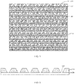
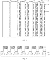
- Figure 1 to Figure 12 are schematic structural diagrams corresponding to steps of a memory forming method according to a first embodiment of the present application.
- a substrate 100 is provided.
- the substrate 100 includes at least word line structures 102 and active regions 101, and bottom dielectric layers 110 and bit line contact layers 120 located on a top surface of the substrate 100.
- the dielectric layers have bit line contact openings 111.
- the bit line contact openings 111 expose the active regions 101 in the substrate 100.
- the bit line contact layers 120 cover the bottom dielectric layers 110 and fill the bit line contact openings 111.
- the substrate 100 includes at least word line structures 102 and active regions 101.
- Figure 1 shows an extension direction 10 of the word line structures, that is, the dashed line 10 in the figure.
- a plurality of active regions 101 are spaced parallel to each other, and for the active regions 101 in column i and the active regions 101 in column i+3, different active regions 101 are located at the same horizontal position in a direction perpendicular to the extension direction 10 of the word line structures.
- the active regions 101 in column i and the active regions 101 in adjacent columns (column i+1 and column i-1) are located at different horizontal positions in the direction perpendicular to the extension direction 10 of the word line structures.
- Middle parts of the active regions 101 separated by the word line structures 102 arranged alternately are bit line contact points, which are used for connecting bit line structures subsequently formed.
- the substrate 100 further includes other memory structures in addition to the word line structures 102 and the active regions 101, such as shallow trench isolation structures. Since the other memory structures do not involve the core technology of the present application, they are not described in detail herein. Those skilled in the art can understand that the substrate 100 further includes other memory structures in addition to the word line structures 102 and the active regions 101, which are used for normal operation of a memory.
- the substrate 100 may be made of sapphire, silicon, silicon carbide, gallium arsenide, aluminum nitride, zinc oxide, or the like.
- the substrate 100 is made of a silicon material. It is understood by those skilled in the art that the use of the silicon material as the substrate 100 is intended to facilitate the understanding of subsequent formation methods by those skilled in the art and does not constitute any limitation. In an actual application process, an appropriate substrate material can be selected as required.
- bottom dielectric layers 110 and bit line contact layers 120 are formed on a top surface of the substrate 100.
- the bottom dielectric layers 110 have bit line contact openings 111.
- the bit line contact openings 111 expose the active regions 101 in the substrate 100.
- the bit line contact layers 120 cover the bottom dielectric layers 110 and fill the bit line contact openings 111.
- bottom dielectric layers 110 are formed on a top surface of the substrate 100.
- the bottom dielectric layers 110 have bit line contact openings 111.
- the bit line contact openings 111 are configured to expose the active regions 101 in the substrate 100.
- the bit line contact openings 111 are configured to expose bit line contact points, that is, expose middle parts of the active regions 101 separated by the word line structures 102.
- the bottom dielectric layers 110 are configured to isolate the bit line structures 200 at positions of non-bit line contact points from the active regions 101.
- the bottom dielectric layer is made of silicon nitride.
- the bottom dielectric layer may also be made of an insulating material such as silicon oxide or silicon oxynitride.
- Figure 3 is a schematic top view of the substrate 100.
- Figure 3 shows positions where bit line structures 200 are required to be subsequently formed.
- Figure 3 shows an extension direction 20 of the bit line structures, that is, the dashed line 20 in the figure.
- the bit line structures 200 are connected to bit line contact points of a column of active regions 101.
- bit line contact layers 120 are formed on a top surface of the substrate 100.
- the bit line contact layers 120 cover the bottom dielectric layers 120 and fill the bit line contact openings 111.
- Figure 4 shows positions where bit line structures 200 are required to be subsequently formed.
- the bit lines connected to the active regions 101 and the bit lines located on the bottom dielectric layers 110 are arranged alternately in any section along the extension direction 10 of the word line structures.
- bit line contact layers 120 are made of a polysilicon material, which is used for the bit lines structure 200 subsequently formed to connect the active regions 101 in the substrate 100 through the bit line contact openings 111.
- bit line contact layers 120 are etched to form bit line contact layers 121 of different heights.
- bit line contact layers 121 of different heights are as follows: the bit line contact layers 121 are used for subsequently forming conductive layers, the conductive layers are at different heights.
- photolithographic mask layers 130 are formed on the top surfaces of the bit line contact layers 120, and photoresists 140 are formed on top surfaces of the photolithographic mask layers 130.
- the photolithographic mask layers 130 are patterned, and patterns 131 arranged at intervals are formed in the direction perpendicular to the extension direction 10 of the word line structures.
- the patterns 131 arranged at intervals are extended strips arranged at intervals.
- Figure 7 shows positions of three kinds of patterns 131 arranged at intervals formed by patterning the photolithographic mask layers 130 based on the photoresists 140, which are specifically as follows: Positions of the first kind of patterns 131 arranged at intervals: Patterns I 401 expose only positions where bit line structures are required to be subsequently formed.
- the patterns I 401 cover at least one position where bit line structures are required to be subsequently formed and completely cover gaps between the bit line structures, only a position where at least one bit line structure is required to be subsequently formed is exposed between adjacent patterns I 401, and the bit line structures covered by the patterns I 401 and the bit line structures not covered by the patterns 1401 are arranged alternately in the extension direction 10 of the word line structures.
- Patterns II 402 cover at least one bit line structure and positions of gaps between part of the bit line structures.
- the patterns II 402 cover at least one position where bit line structures are required to be subsequently formed and cover part of gaps between the bit line structures, only a position where at least one bit line structure is required to be subsequently formed and the part of gaps between the bit line structures are exposed between adjacent patterns II 402, and the bit line structures covered by the patterns II 402 and the bit line structures not covered by the patterns II 402 are arranged alternately in the extension direction 10 of the word line structures.
- Patterns III 403 cover only a position of at least one bit line structure.
- the patterns III 403 cover at least one position where bit line structures are required to be subsequently formed, only gaps between the bit line structures and a position where at least one bit line structure is required to be subsequently formed are exposed between adjacent patterns III 403, and the bit line structures covered by the patterns III 403 and the bit line structures not covered by the patterns III 403 are arranged alternately in the extension direction 10 of the word line structures.
- bit line contact layers 120 are etched based on the patterns 131 arranged at intervals to form bit line contact layers 121 of different heights.
- Figure 9 shows a schematic cross-sectional view in directions of the dashed line 30 and the dashed line 31.
- the bit line contact layers 121 are at the same height in a direction perpendicular to the extension direction 10 of the word line structures (the same vertical position of the two figures). In the extension direction 10 of the word line structures (section direction illustrated), the bit line contact layers 121 are at different heights, and convex portions at the first height and concave parts at the second height are arranged alternately.
- masks may also be continuously formed to further etch the bit line contact layers of different heights, so that the heights of top surfaces of the remaining bit line contact layers may be arranged alternately in a preset height order.
- conductive layers 140 are formed on top surfaces of the bit line contact layers 121 at different heights.
- conductive films 141 are formed on top surfaces of the bit line contact layers 121 at different heights.
- the conductive films 141 are etched to form conductive layers 140 with a uniform thickness on the top surfaces of the bit line contact layers 121 at different heights.
- the conductive layers 140 on the top surfaces of the bit line contact layers 121 at different heights are ensured to be at different heights by forming the conductive layers 140 with a uniform thickness.
- the thicknesses of the conductive layers on the top surfaces of the bit line contact layers at different heights may be different, but this needs to ensure that the top surfaces of the conductive layers are at different heights, so that a connecting line of the conductive layers between different bit line structures is oblique, thus the spacing of the conductive layers between the bit line structures is increased on the basis of not changing the arrangement of the bit line structures.
- Top surfaces of the formed conductive layers 140 are at the same height in a direction perpendicular to the extension direction 10 of the word line structures; and the top surfaces are at different heights in the extension direction 10 of the word line structures.
- the conductive layers 140 are made of one conductive material or multiple conductive materials, such as doped polysilicon, titanium, titanium nitride, tungsten, and tungsten compounds.
- top dielectric layers 150 are formed on the top surfaces of the conductive layers 140.
- top dielectric films are formed on the top surfaces of the conductive layers, top surfaces of the top dielectric films are planarized to form the top dielectric layers 150, and top surfaces of the top dielectric layers 150 are at a uniform height.
- the top surfaces of the top dielectric films are planarized by chemical mechanical polishing. Compared with etching, chemical mechanical polishing has a higher removal rate, which is conducive to shortening a process cycle.
- the material of the top dielectric layers 150 includes silicon nitride, silicon oxynitride, silicon oxide, or other materials.
- the top dielectric layers 150 are made of a nitrogen-containing insulating material, that is, the top dielectric layers 150 are made of a silicon nitride material.
- part of the top dielectric layers 150, part of the conductive layers 140, and part of the bit line contact layers 121 at different heights are sequentially etched to form discrete bit line structures 200.
- a connecting line of the conductive layers 140 in the discrete bit line structures 200 is straight in the direction perpendicular to the extension direction 10 of the word line structure, and conductive layers 140 in adjacent discrete bit line structures 200 are at different heights in the extension direction 10 of the word line structures.
- bit line contact layers at different heights are formed, so that conductive layers formed on top surfaces of the bit line contact layers are at different heights.
- Top surfaces of the conductive layers are at the same height in a direction perpendicular to an extension direction of the word line structures, and the top surfaces of the conductive layers are at different heights in the extension direction of the word line structures, that is, in discrete bit line structures subsequently formed, the conductive layers in the same bit line structure are at the same height, and the conductive layers in different bit line structures are at different heights.
- the conductive layers in adjacent discrete bit line structures are at different heights, and compared with the conductive layers at the same height, a distance between the conductive layers at different heights changes from a horizontal distance to a slant distance, thus the spacing between the conductive layers is increased in the bit line structures. Further, parasitic capacitance between the bit line structures is reduced and a saturation current of the memory is increased.
- the memory forming method according to the present embodiment features a simple process, a low cost, and easy implementation.
- a second embodiment of the present application relates to a memory.
- the memory includes: a substrate 100 including at least word line structures 102 and active regions 101; bottom dielectric layers 110 located at the top of the substrate 100, the bottom dielectric layers 110 having bit line contact openings 111 exposing the active regions 101 in the substrate; and discrete bit line structures 200, top surfaces of the bit line structures 200 being at the same height, and the bit line structures 200 including: bit line contact layers 121 located at the top of the bottom dielectric layers 110 and the bit line contact openings 111, conductive layers 140 located at the top of the bit line contact layers 121, and top dielectric layers 150 located at the top of the conductive layers 140; where the conductive layers 140 in the same bit line structure are at the same height in an extension direction 20 of the bit line structures, and the conductive layers 140 in adjacent bit line structures are at different heights in the extension direction 10 of the word line structures.
- the substrate 100 further includes other memory structures in addition to the word line structures 102 and the active regions 101, such as shallow trench isolation structures. Since the other memory structures do not involve the core technology of the present application, they are not described in detail herein. Those skilled in the art can understand that the substrate 100 further includes other memory structures in addition to the word line structures 102 and the active regions 101, which are used for normal operation of a memory.
- the thicknesses of the conductive layers 140 are uniform. In other embodiments, the thicknesses of the conductive layers 140 on the top surfaces of the bit line contact layers 121 at different heights may be different, but this needs to ensure that the top surfaces of the conductive layers 140 are at different heights, so that a connecting line of the conductive layers between different bit line structures is oblique, thus the spacing of the conductive layers between the bit line structures is increased on the basis of not changing the arrangement of the bit line structures.
- the connecting line of the conductive layers 140 is straight, that is, in the same bit line structure 200, the conductive layers 140 are at the same height (the same height at the bottom and the same height at the top).
- the conductive layers 140 at the first height and the conductive layers 140 at the second height are arranged alternately in the extension direction 10 of the word line structures. In other embodiments, the conductive layers 140 may be arranged alternately in a preset height order.
- bit line contact layers at different heights are formed, so that conductive layers formed on top surfaces of the bit line contact layers are at different heights.
- Top surfaces of the conductive layers are at the same height in a direction perpendicular to an extension direction of the word line structures, and the top surfaces of the conductive layers are at different heights in the extension direction of the word line structures, that is, in discrete bit line structures subsequently formed, the conductive layers in the same bit line structure are at the same height, and the conductive layers in different bit line structures are at different heights.
- the conductive layers in adjacent discrete bit line structures are at different heights, and compared with the conductive layers at the same height, a distance between the conductive layers at different heights changes from a horizontal distance to a slant distance, thus the spacing between the conductive layers is increased in the bit line structures. Further, parasitic capacitance between the bit line structures is reduced and a saturation current of the memory is increased.
- the memory forming method according to the present embodiment features a simple process, a low cost, and easy implementation.
- the present embodiment may be implemented in conjunction with the first embodiment.
- Related technical details mentioned in the first embodiment are still valid in the present embodiment, and a technical effect achieved in the first embodiment may also be achieved in the present embodiment, which is not described herein again to reduce repetition. Accordingly, related technical details mentioned in the present embodiment may also be applied to the first embodiment.
Landscapes
- Engineering & Computer Science (AREA)
- Manufacturing & Machinery (AREA)
- Semiconductor Memories (AREA)
- Internal Circuitry In Semiconductor Integrated Circuit Devices (AREA)
Abstract
Description
- This application claims priority to
Chinese Patent Application No. 202010576479.9, entitled "MEMORY FORMING METHOD AND MEMORY", filed on June 22, 2020 - The present application relates to the field of semiconductor technologies, in particular to a memory forming method and a memory.
- With constant decrease in a feature size and a line width of a dynamic random access memory (DRAM), spacing between adjacent bit line structures becomes smaller and smaller. The smaller spacing between adjacent bit line structures may lead to continuous increase of parasitic capacitance between the adjacent bit line structures, which affects a saturation current in a DRAM array region and then affects the operation efficiency of the DRAM
- With the constant decrease in the line width of the DRAM, how to increase spacing between bit line structures is an urgent problem to be solved.
- An objective of some embodiments of the present application is to provide a memory forming method and a memory, which increases spacing between the conductive layers in the bit line structures on the basis of not changing the arrangement of the bit line structures by forming conductive layers at different heights in bit line structures.
- Embodiments of the present application provide a memory forming method, including: providing a substrate, wherein the substrate includes at least word line structures and active regions, and bottom dielectric layers and bit line contact layers located on a top surface of the substrate, the bottom dielectric layer have bit line contact openings exposing the active regions in the substrate, and the bit line contact layers cover the bottom dielectric layers and fill the bit line contact openings; etching part of the bit line contact layers to form the bit line contact layers of different heights; forming conductive layers on top surfaces of the bit line contact layers, top surfaces of the conductive layers being at the same height in a direction perpendicular to an extension direction of the word line structures; and the top surfaces of the conductive layers being at different heights in the extension direction of the word line structures; forming top dielectric layers on the top surfaces of the conductive layers; and sequentially etching part of the top dielectric layers, part of the conductive layers, and part of the bit line contact layers to form discrete bit line structures.
- In addition, the etching art of the bit line contact layers to form the bit line contact layers of different heights includes: forming photolithographic mask layers on the top surfaces of the bit line contact layers; patterning the photolithographic mask layers, and forming patterns arranged at intervals in the direction perpendicular to the extension direction of the word line structures; etching part of the bit line contact layers based on the patterns arranged at intervals to form the bit line contact layers of different heights; and removing the patterns arranged at intervals.
- Furthermore, the patterns arranged at intervals are extended strips arranged at intervals.
- Furthermore, after the sequentially etching part of the top dielectric layers, part of the conductive layers, and part of the bit line contact layers to form discrete bit line structures, a connecting line of the conductive layers in the bit line structures is straight in the direction perpendicular to the extension direction of the word line structure, and conductive layers in adjacent discrete bit line structures are at different heights in the extension direction of the word line structure.
- Furthermore, the forming conductive layers on top surfaces of the bit line contact layers includes: forming conductive films on the top surfaces of the bit line contact layers; and etching the conductive films to form the conductive layers with a uniform thickness on the top surfaces of the bit line contact layers at different heights. The conductive layers on the top surfaces of the bit line contact layers at different heights are ensured to be at different heights by forming the conductive layers with a uniform thickness.
- Furthermore, the forming top dielectric layers on the top surfaces of the conductive layers includes: forming top dielectric films on the top surfaces of the conductive layers; and planarizing top surfaces of the top dielectric films to form the top dielectric layers, top surfaces of the top dielectric layers being at a uniform height.
- The embodiments of the present application further provide a memory, including: a substrate, wherein the substrate includes at least word line structures and active regions; bottom dielectric layers, located at the top of the substrate, wherein the bottom dielectric layers have bit line contact openings exposing the active regions in the substrate; and discrete bit line structures, top surfaces of the bit line structures being at the same height, wherein the bit line structures includes: bit line contact layers located at the top of the bottom dielectric layers and in the bit line contact openings, conductive layers located at the top of the bit line contact layers, and top dielectric layers located at the top of the conductive layers; wherein the conductive layers in the same bit line structure are at the same height in an extension direction of the bit line structures, and the conductive layers in adjacent bit line structures are at different heights in the extension direction of the word line structures.
- Furthermore, the conductive layers in the discrete bit line structures have a uniform thickness. Through the conductive layers with the uniform thickness, the conductive layers on the top surfaces of the bit line contact layers at different heights are ensured to be at different heights.
- Furthermore, a connecting line of the conductive layers is straight in the extension direction of the bit line structures.
- Furthermore, a connecting line of the conductive layers is straight in the extension direction of the word line structures.
- Compared with the prior art, in the embodiments of the present application, bit line contact layers at different heights are formed, so that conductive layers formed on top surfaces of the bit line contact layers are at different heights. Top surfaces of the conductive layers are at the same height in a direction perpendicular to an extension direction of the word line structures, and the top surfaces of the conductive layers are at different heights in the extension direction of the word line structures, that is, in discrete bit line structures subsequently formed, the conductive layers in the same bit line structure are at the same height, and the conductive layers in different bit line structures are at different heights. On the basis of not changing the arrangement of the bit line structures, the conductive layers in adjacent discrete bit line structures are at different heights, and compared with the conductive layers at the same height, a distance between the conductive layers at different heights changes from a horizontal distance to a slant distance, thus the spacing between the conductive layers is increased in the bit line structures. Further, parasitic capacitance between the bit line structures is reduced and a saturation current of the memory is increased. At the same time, the memory forming method according to the present embodiment features a simple process, a low cost, and easy implementation.
- One or more embodiments are shown by way of exemplary description, and not by limitation, in the figures of the accompanying drawings. The figures in the drawings are not to scale, unless otherwise stated.
-
Figure 1 to Figure 12 are schematic structural diagrams corresponding to steps of a memory forming method according to a first embodiment of the present application; and -
Figure 13 is a schematic cross-sectional view of a memory formed according to the first embodiment of the present application. - With constant decrease in a feature size and a line width of a DRAM, spacing between adjacent bit line structures becomes smaller and smaller. The smaller spacing between adjacent bit line structures may lead to continuous increase of parasitic capacitance between the adjacent bit line structures, which affects a saturation current in a DRAM array region and then affects the operation efficiency of the DRAM
- In order to make the objectives, technical solutions, and advantages of the present application clearer, some embodiments of the present application are described in further detail below with reference to the accompanying drawings and embodiments. It should be understood that specific embodiments described herein are intended only to interpret the present application and are not intended to limit the present application.
- A first embodiment of the present application provides a memory forming method, including: providing a substrate, including at least word line structures and active regions, and bottom dielectric layers and bit line contact layers located on a top surface of the substrate, the bottom dielectric layer having bit line contact openings exposing the active regions in the substrate, and the bit line contact layers covering the bottom dielectric layers and filling the bit line contact openings; etching part of the bit line contact layers to form the bit line contact layers of different heights; forming conductive layers on top surfaces of the bit line contact layers, top surfaces of the conductive layers being at the same height in a direction perpendicular to an extension direction of the word line structures; and the top surfaces of the conductive layers being at different heights in the extension direction of the word line structures; forming top dielectric layers on the top surfaces of the conductive layers; and sequentially etching part of the top dielectric layers, part of the conductive layers, and part of the bit line contact layers to form discrete bit line structures.
-
Figure 1 to Figure 12 are schematic structural diagrams corresponding to steps of a memory forming method according to a first embodiment of the present application. - Referring to
Figure 1 to Figure 5 , asubstrate 100 is provided. Thesubstrate 100 includes at leastword line structures 102 andactive regions 101, and bottomdielectric layers 110 and bitline contact layers 120 located on a top surface of thesubstrate 100. The dielectric layers have bit line contact openings 111. The bit line contact openings 111 expose theactive regions 101 in thesubstrate 100. The bitline contact layers 120 cover the bottomdielectric layers 110 and fill the bit line contact openings 111. - Referring to
Figure 1 , asubstrate 100 is provided. Thesubstrate 100 includes at leastword line structures 102 andactive regions 101. -
Figure 1 shows anextension direction 10 of the word line structures, that is, thedashed line 10 in the figure. - A plurality of
active regions 101 are spaced parallel to each other, and for theactive regions 101 in column i and theactive regions 101 in column i+3, differentactive regions 101 are located at the same horizontal position in a direction perpendicular to theextension direction 10 of the word line structures. Theactive regions 101 in column i and theactive regions 101 in adjacent columns (column i+1 and column i-1) are located at different horizontal positions in the direction perpendicular to theextension direction 10 of the word line structures. Middle parts of theactive regions 101 separated by theword line structures 102 arranged alternately are bit line contact points, which are used for connecting bit line structures subsequently formed. - It should be noted that the
substrate 100 further includes other memory structures in addition to theword line structures 102 and theactive regions 101, such as shallow trench isolation structures. Since the other memory structures do not involve the core technology of the present application, they are not described in detail herein. Those skilled in the art can understand that thesubstrate 100 further includes other memory structures in addition to theword line structures 102 and theactive regions 101, which are used for normal operation of a memory. - The
substrate 100 may be made of sapphire, silicon, silicon carbide, gallium arsenide, aluminum nitride, zinc oxide, or the like. In the present embodiment, thesubstrate 100 is made of a silicon material. It is understood by those skilled in the art that the use of the silicon material as thesubstrate 100 is intended to facilitate the understanding of subsequent formation methods by those skilled in the art and does not constitute any limitation. In an actual application process, an appropriate substrate material can be selected as required. - Referring to
Figure 2 to Figure 5 , bottomdielectric layers 110 and bitline contact layers 120 are formed on a top surface of thesubstrate 100. The bottomdielectric layers 110 have bit line contact openings 111. The bit line contact openings 111 expose theactive regions 101 in thesubstrate 100. The bitline contact layers 120 cover the bottomdielectric layers 110 and fill the bit line contact openings 111. - Referring to
Figure 2 , bottomdielectric layers 110 are formed on a top surface of thesubstrate 100. The bottomdielectric layers 110 have bit line contact openings 111. The bit line contact openings 111 are configured to expose theactive regions 101 in thesubstrate 100. Specifically, the bit line contact openings 111 are configured to expose bit line contact points, that is, expose middle parts of theactive regions 101 separated by theword line structures 102. - The bottom dielectric layers 110 are configured to isolate the
bit line structures 200 at positions of non-bit line contact points from theactive regions 101. In the present embodiment, the bottom dielectric layer is made of silicon nitride. In other embodiments, the bottom dielectric layer may also be made of an insulating material such as silicon oxide or silicon oxynitride. - Referring to
Figure 3, Figure 3 is a schematic top view of thesubstrate 100. On the basis of the bottom dielectric layers 110 formed inFigure 2 ,Figure 3 shows positions wherebit line structures 200 are required to be subsequently formed.Figure 3 shows anextension direction 20 of the bit line structures, that is, the dashedline 20 in the figure. Thebit line structures 200 are connected to bit line contact points of a column ofactive regions 101. - Referring to
Figure 4 , bit line contact layers 120 are formed on a top surface of thesubstrate 100. The bit line contact layers 120 cover the bottom dielectric layers 120 and fill the bit line contact openings 111.Figure 4 shows positions wherebit line structures 200 are required to be subsequently formed. The bit lines connected to theactive regions 101 and the bit lines located on the bottom dielectric layers 110 are arranged alternately in any section along theextension direction 10 of the word line structures. - In the present embodiment, the bit line contact layers 120 are made of a polysilicon material, which is used for the
bit lines structure 200 subsequently formed to connect theactive regions 101 in thesubstrate 100 through the bit line contact openings 111. - Referring to
Figure 5 to Figure 8 , part of the bit line contact layers 120 are etched to form bit line contact layers 121 of different heights. - The reason for forming the bit line contact layers 121 of different heights is as follows: the bit line contact layers 121 are used for subsequently forming conductive layers, the conductive layers are at different heights.
- Specifically, referring to
Figure 5 , photolithographic mask layers 130 are formed on the top surfaces of the bit line contact layers 120, andphotoresists 140 are formed on top surfaces of the photolithographic mask layers 130. - Referring to
Figure 6 , the photolithographic mask layers 130 are patterned, andpatterns 131 arranged at intervals are formed in the direction perpendicular to theextension direction 10 of the word line structures. Thepatterns 131 arranged at intervals are extended strips arranged at intervals. - Referring to
Figure 7, Figure 7 shows positions of three kinds ofpatterns 131 arranged at intervals formed by patterning the photolithographic mask layers 130 based on thephotoresists 140, which are specifically as follows:
Positions of the first kind ofpatterns 131 arranged at intervals: Patterns I 401 expose only positions where bit line structures are required to be subsequently formed. - Specifically, the patterns I 401 cover at least one position where bit line structures are required to be subsequently formed and completely cover gaps between the bit line structures, only a position where at least one bit line structure is required to be subsequently formed is exposed between adjacent patterns I 401, and the bit line structures covered by the patterns I 401 and the bit line structures not covered by the patterns 1401 are arranged alternately in the
extension direction 10 of the word line structures. - Positions of the second kind of
patterns 131 arranged at intervals:Patterns II 402 cover at least one bit line structure and positions of gaps between part of the bit line structures. - Specifically, the patterns II 402 cover at least one position where bit line structures are required to be subsequently formed and cover part of gaps between the bit line structures, only a position where at least one bit line structure is required to be subsequently formed and the part of gaps between the bit line structures are exposed between adjacent patterns II 402, and the bit line structures covered by the patterns II 402 and the bit line structures not covered by the
patterns II 402 are arranged alternately in theextension direction 10 of the word line structures. - Positions of the third kind of
patterns 131 arranged at intervals:Patterns III 403 cover only a position of at least one bit line structure. - Specifically, the
patterns III 403 cover at least one position where bit line structures are required to be subsequently formed, only gaps between the bit line structures and a position where at least one bit line structure is required to be subsequently formed are exposed betweenadjacent patterns III 403, and the bit line structures covered by thepatterns III 403 and the bit line structures not covered by thepatterns III 403 are arranged alternately in theextension direction 10 of the word line structures. - Referring to
Figure 8 , part of the bit line contact layers 120 are etched based on thepatterns 131 arranged at intervals to form bit line contact layers 121 of different heights. - Referring to
Figure 9 , thepatterns 131 arranged at intervals are removed. - Directions of the dashed
line 30 and the dashedline 31 in the figure are two section positions shown inFigure 3 , for those skilled in the art to understand the principle of the present application. -
Figure 9 shows a schematic cross-sectional view in directions of the dashedline 30 and the dashedline 31. The bit line contact layers 121 are at the same height in a direction perpendicular to theextension direction 10 of the word line structures (the same vertical position of the two figures). In theextension direction 10 of the word line structures (section direction illustrated), the bit line contact layers 121 are at different heights, and convex portions at the first height and concave parts at the second height are arranged alternately. - In other embodiments, masks may also be continuously formed to further etch the bit line contact layers of different heights, so that the heights of top surfaces of the remaining bit line contact layers may be arranged alternately in a preset height order.
- Referring to
Figure 10 to Figure 11 ,conductive layers 140 are formed on top surfaces of the bit line contact layers 121 at different heights. - Specifically, referring to
Figure 10 ,conductive films 141 are formed on top surfaces of the bit line contact layers 121 at different heights. - Referring to
Figure 11 , the conductive films 141 (refer toFigure 10 ) are etched to formconductive layers 140 with a uniform thickness on the top surfaces of the bit line contact layers 121 at different heights. Theconductive layers 140 on the top surfaces of the bit line contact layers 121 at different heights are ensured to be at different heights by forming theconductive layers 140 with a uniform thickness. - In other embodiments, the thicknesses of the conductive layers on the top surfaces of the bit line contact layers at different heights may be different, but this needs to ensure that the top surfaces of the conductive layers are at different heights, so that a connecting line of the conductive layers between different bit line structures is oblique, thus the spacing of the conductive layers between the bit line structures is increased on the basis of not changing the arrangement of the bit line structures.
- Top surfaces of the formed
conductive layers 140 are at the same height in a direction perpendicular to theextension direction 10 of the word line structures; and the top surfaces are at different heights in theextension direction 10 of the word line structures. - In the present embodiment, the
conductive layers 140 are made of one conductive material or multiple conductive materials, such as doped polysilicon, titanium, titanium nitride, tungsten, and tungsten compounds. - Referring to
Figure 12 , topdielectric layers 150 are formed on the top surfaces of theconductive layers 140. - Specifically, top dielectric films are formed on the top surfaces of the conductive layers, top surfaces of the top dielectric films are planarized to form the top
dielectric layers 150, and top surfaces of the topdielectric layers 150 are at a uniform height. - Specifically, the top surfaces of the top dielectric films are planarized by chemical mechanical polishing. Compared with etching, chemical mechanical polishing has a higher removal rate, which is conducive to shortening a process cycle.
- In the present embodiment, the material of the top
dielectric layers 150 includes silicon nitride, silicon oxynitride, silicon oxide, or other materials. In the present embodiment, the topdielectric layers 150 are made of a nitrogen-containing insulating material, that is, the topdielectric layers 150 are made of a silicon nitride material. - Referring to
Figure 13 , part of the topdielectric layers 150, part of theconductive layers 140, and part of the bit line contact layers 121 at different heights are sequentially etched to form discretebit line structures 200. - A connecting line of the
conductive layers 140 in the discretebit line structures 200 is straight in the direction perpendicular to theextension direction 10 of the word line structure, andconductive layers 140 in adjacent discretebit line structures 200 are at different heights in theextension direction 10 of the word line structures. - Compared with the prior art, in the present embodiment, according to the memory forming method provided in the embodiment of the present application, bit line contact layers at different heights are formed, so that conductive layers formed on top surfaces of the bit line contact layers are at different heights. Top surfaces of the conductive layers are at the same height in a direction perpendicular to an extension direction of the word line structures, and the top surfaces of the conductive layers are at different heights in the extension direction of the word line structures, that is, in discrete bit line structures subsequently formed, the conductive layers in the same bit line structure are at the same height, and the conductive layers in different bit line structures are at different heights. On the basis of not changing the arrangement of the bit line structures, the conductive layers in adjacent discrete bit line structures are at different heights, and compared with the conductive layers at the same height, a distance between the conductive layers at different heights changes from a horizontal distance to a slant distance, thus the spacing between the conductive layers is increased in the bit line structures. Further, parasitic capacitance between the bit line structures is reduced and a saturation current of the memory is increased. At the same time, the memory forming method according to the present embodiment features a simple process, a low cost, and easy implementation.
- The division of the above steps is only for clear illustration. In implementation, the steps may be combined into one step or some steps may be split into a plurality of steps. These steps, as long as observing the same logical relationship, all fall within the protection scope of the present application. Any non-mandatory modifications added to the flow or any optional designs introduced to the same shall fall within the protection scope of the present application provided that the core design of the procedures is not changed.
- A second embodiment of the present application relates to a memory.
- Referring to
Figure 13 , the memory according to the present embodiment will be described in detail below with reference to the drawings, and the parts the same as or corresponding to the first embodiment will not be described in detail below. - The memory includes: a
substrate 100 including at leastword line structures 102 andactive regions 101; bottom dielectric layers 110 located at the top of thesubstrate 100, the bottom dielectric layers 110 having bit line contact openings 111 exposing theactive regions 101 in the substrate; and discretebit line structures 200, top surfaces of thebit line structures 200 being at the same height, and thebit line structures 200 including: bit line contact layers 121 located at the top of the bottom dielectric layers 110 and the bit line contact openings 111,conductive layers 140 located at the top of the bit line contact layers 121, and topdielectric layers 150 located at the top of theconductive layers 140; where theconductive layers 140 in the same bit line structure are at the same height in anextension direction 20 of the bit line structures, and theconductive layers 140 in adjacent bit line structures are at different heights in theextension direction 10 of the word line structures. - It should be noted that the
substrate 100 further includes other memory structures in addition to theword line structures 102 and theactive regions 101, such as shallow trench isolation structures. Since the other memory structures do not involve the core technology of the present application, they are not described in detail herein. Those skilled in the art can understand that thesubstrate 100 further includes other memory structures in addition to theword line structures 102 and theactive regions 101, which are used for normal operation of a memory. - In the present embodiment, the thicknesses of the
conductive layers 140 are uniform. In other embodiments, the thicknesses of theconductive layers 140 on the top surfaces of the bit line contact layers 121 at different heights may be different, but this needs to ensure that the top surfaces of theconductive layers 140 are at different heights, so that a connecting line of the conductive layers between different bit line structures is oblique, thus the spacing of the conductive layers between the bit line structures is increased on the basis of not changing the arrangement of the bit line structures. - In the present embodiment, in the extension direction of the bit line structures, the connecting line of the
conductive layers 140 is straight, that is, in the samebit line structure 200, theconductive layers 140 are at the same height (the same height at the bottom and the same height at the top). - In the present embodiment, the
conductive layers 140 at the first height and theconductive layers 140 at the second height are arranged alternately in theextension direction 10 of the word line structures. In other embodiments, theconductive layers 140 may be arranged alternately in a preset height order. - Compared with the prior art, bit line contact layers at different heights are formed, so that conductive layers formed on top surfaces of the bit line contact layers are at different heights. Top surfaces of the conductive layers are at the same height in a direction perpendicular to an extension direction of the word line structures, and the top surfaces of the conductive layers are at different heights in the extension direction of the word line structures, that is, in discrete bit line structures subsequently formed, the conductive layers in the same bit line structure are at the same height, and the conductive layers in different bit line structures are at different heights. On the basis of not changing the arrangement of the bit line structures, the conductive layers in adjacent discrete bit line structures are at different heights, and compared with the conductive layers at the same height, a distance between the conductive layers at different heights changes from a horizontal distance to a slant distance, thus the spacing between the conductive layers is increased in the bit line structures. Further, parasitic capacitance between the bit line structures is reduced and a saturation current of the memory is increased. At the same time, the memory forming method according to the present embodiment features a simple process, a low cost, and easy implementation.
- Since the first embodiment corresponds to the present embodiment, the present embodiment may be implemented in conjunction with the first embodiment. Related technical details mentioned in the first embodiment are still valid in the present embodiment, and a technical effect achieved in the first embodiment may also be achieved in the present embodiment, which is not described herein again to reduce repetition. Accordingly, related technical details mentioned in the present embodiment may also be applied to the first embodiment.
- Those of ordinary skill in the art may understand that the above embodiments are specific embodiments for implementing the present application. In practical applications, various changes may be made to the forms and details of these embodiments without departing from the spirit and scope of the present application.
Claims (10)
- A memory forming method, comprising:providing a substrate, wherein the substrate comprises at least word line structures and active regions, and bottom dielectric layers and bit line contact layers located on a top surface of the substrate, the bottom dielectric layer have bit line contact openings exposing the active regions in the substrate, and the bit line contact layers cover the bottom dielectric layers and fill the bit line contact openings;etching part of the bit line contact layers to form the bit line contact layers of different heights;forming conductive layers on top surfaces of the bit line contact layers, top surfaces of the conductive layers being at the same height in a direction perpendicular to an extension direction of the word line structures; and the top surfaces of the conductive layers being at different heights in the extension direction of the word line structures;forming top dielectric layers on the top surfaces of the conductive layers; andsequentially etching part of the top dielectric layers, part of the conductive layers, and part of the bit line contact layers to form discrete bit line structures.
- The memory forming method according to claim 1, wherein the etching part of the bit line contact layers to form the bit line contact layers of different heights comprises:forming photolithographic mask layers on the top surfaces of the bit line contact layers;patterning the photolithographic mask layers, and forming patterns arranged at intervals in the direction perpendicular to the extension direction of the word line structures;etching part of the bit line contact layers based on the patterns arranged at intervals to form the bit line contact layers of different heights; andremoving the patterns arranged at intervals.
- The memory forming method according to claim 2, wherein the patterns arranged at intervals are extended strips arranged at intervals.
- The memory forming method according to claim 1, wherein after the sequentially etching part of the top dielectric layers, part of the conductive layers, and part of the bit line contact layers to form discrete bit line structures, a connecting line of the conductive layers in the bit line structures is straight in the direction perpendicular to the extension direction of the word line structure, and conductive layers in adjacent discrete bit line structures are at different heights in the extension direction of the word line structure.
- The memory forming method according to claim 1, wherein the forming conductive layers on top surfaces of the bit line contact layers comprises:forming conductive films on the top surfaces of the bit line contact layers; andetching the conductive films to form the conductive layers with a uniform thickness on the top surfaces of the bit line contact layers at different heights.
- The memory forming method according to claim 1, wherein the forming top dielectric layers on the top surfaces of the conductive layers comprises:forming top dielectric films on the top surfaces of the conductive layers; andplanarizing top surfaces of the top dielectric films to form the top dielectric layers, top surfaces of the top dielectric layers being at a uniform height.
- A memory, comprising:a substrate, wherein the substrate comprises at least word line structures and active regions;bottom dielectric layers, located at the top of the substrate, wherein the bottom dielectric layers have bit line contact openings exposing the active regions in the substrate; anddiscrete bit line structures, top surfaces of the bit line structures being at the same height, wherein the bit line structure comprises: bit line contact layers located at the top of the bottom dielectric layers and in the bit line contact openings, conductive layers located at the top of the bit line contact layers, and top dielectric layers located at the top of the conductive layers;wherein the conductive layers in the same bit line structure are at the same height in an extension direction of the bit line structures, and the conductive layers in adjacent bit line structures are at different heights in the extension direction of the word line structures.
- The memory according to claim 7, wherein the conductive layers in the discrete bit line structures have a uniform thickness.
- The memory according to claim 7, wherein a connecting line of the conductive layers is straight in the extension direction of the bit line structures.
- The memory according to claim 7, wherein the conductive layers in the bit line structures are arranged alternately in a preset height order in the extension direction of the word line structures.
Applications Claiming Priority (2)
| Application Number | Priority Date | Filing Date | Title |
|---|---|---|---|
| CN202010576479.9A CN113903709B (en) | 2020-06-22 | 2020-06-22 | Memory forming method and memory |
| PCT/CN2020/115398 WO2021258561A1 (en) | 2020-06-22 | 2020-09-15 | Memory forming method and memory |
Publications (3)
| Publication Number | Publication Date |
|---|---|
| EP4036960A1 true EP4036960A1 (en) | 2022-08-03 |
| EP4036960A4 EP4036960A4 (en) | 2022-12-28 |
| EP4036960B1 EP4036960B1 (en) | 2024-09-04 |
Family
ID=79186622
Family Applications (1)
| Application Number | Title | Priority Date | Filing Date |
|---|---|---|---|
| EP20942413.4A Active EP4036960B1 (en) | 2020-06-22 | 2020-09-15 | Memory forming method and memory |
Country Status (4)
| Country | Link |
|---|---|
| US (1) | US12342535B2 (en) |
| EP (1) | EP4036960B1 (en) |
| CN (1) | CN113903709B (en) |
| WO (1) | WO2021258561A1 (en) |
Families Citing this family (4)
| Publication number | Priority date | Publication date | Assignee | Title |
|---|---|---|---|---|
| CN113764580B (en) | 2020-06-04 | 2023-09-12 | 长鑫存储技术有限公司 | Double-sided capacitor structure and forming method thereof |
| KR102831626B1 (en) * | 2020-06-22 | 2025-07-07 | 창신 메모리 테크놀로지즈 아이엔씨 | How memory is formed and memory |
| CN114023744B (en) * | 2022-01-10 | 2022-03-25 | 长鑫存储技术有限公司 | A kind of semiconductor structure, preparation method of semiconductor structure and semiconductor memory |
| US12363884B2 (en) | 2022-01-10 | 2025-07-15 | Changxin Memory Technologies, Inc. | Three-dimensional memory device with capacitors and vertical word-line |
Family Cites Families (17)
| Publication number | Priority date | Publication date | Assignee | Title |
|---|---|---|---|---|
| KR100486300B1 (en) * | 2003-01-14 | 2005-04-29 | 삼성전자주식회사 | Method for fabricating semiconductor device wherein bit-lines are formed by damascene technique |
| US7139184B2 (en) | 2004-12-07 | 2006-11-21 | Infineon Technologies Ag | Memory cell array |
| KR100689712B1 (en) | 2006-03-23 | 2007-03-08 | 삼성전자주식회사 | Method for manufacturing semiconductor memory device and its structure |
| KR100855579B1 (en) | 2006-10-02 | 2008-09-03 | 삼성전자주식회사 | Semiconductor memory device and forming method thereof |
| KR100976682B1 (en) | 2008-04-04 | 2010-08-18 | 주식회사 하이닉스반도체 | Semiconductor memory device and manufacturing method thereof |
| KR101077290B1 (en) * | 2009-04-24 | 2011-10-26 | 주식회사 하이닉스반도체 | Semiconductor memory device and fabrication method thereof |
| KR101648128B1 (en) * | 2009-12-28 | 2016-08-24 | 삼성전자주식회사 | Method for forming fine pattern having variable width and method for manufacturing semiconductor device using the same |
| KR101610831B1 (en) | 2010-02-09 | 2016-04-12 | 삼성전자주식회사 | Semiconductor device having bit line interconnection with enlarged width and lowered level on bit line contact and fabricating methods of the same |
| KR101658492B1 (en) * | 2010-08-13 | 2016-09-21 | 삼성전자주식회사 | Method for forming fine patterns and method for manufacturing a semiconductor device by using the same |
| KR102489949B1 (en) * | 2016-12-13 | 2023-01-17 | 삼성전자주식회사 | Semiconductor device and method for fabricating the same |
| KR102630510B1 (en) | 2017-09-19 | 2024-01-30 | 삼성전자주식회사 | Semiconductor memory device and method of forming the same |
| KR102396583B1 (en) | 2017-11-09 | 2022-05-11 | 삼성전자주식회사 | Memory device and method of manufacturing the same |
| CN107910330B (en) | 2017-11-29 | 2023-09-19 | 长鑫存储技术有限公司 | Dynamic random access memory array and its layout structure and manufacturing method |
| CN207503976U (en) * | 2017-11-29 | 2018-06-15 | 睿力集成电路有限公司 | Dynamic random access memory array and its domain structure |
| CN208368506U (en) | 2018-06-20 | 2019-01-11 | 长鑫存储技术有限公司 | A semiconductor memory structure |
| CN210272309U (en) * | 2019-08-30 | 2020-04-07 | 长鑫存储技术有限公司 | Semiconductor structure |
| CN110556359B (en) * | 2019-09-17 | 2024-12-20 | 福建省晋华集成电路有限公司 | A bit line structure and semiconductor memory |
-
2020
- 2020-06-22 CN CN202010576479.9A patent/CN113903709B/en active Active
- 2020-09-15 WO PCT/CN2020/115398 patent/WO2021258561A1/en not_active Ceased
- 2020-09-15 US US17/601,494 patent/US12342535B2/en active Active
- 2020-09-15 EP EP20942413.4A patent/EP4036960B1/en active Active
Also Published As
| Publication number | Publication date |
|---|---|
| WO2021258561A1 (en) | 2021-12-30 |
| EP4036960B1 (en) | 2024-09-04 |
| CN113903709A (en) | 2022-01-07 |
| US12342535B2 (en) | 2025-06-24 |
| EP4036960A4 (en) | 2022-12-28 |
| CN113903709B (en) | 2024-08-02 |
| US20220328494A1 (en) | 2022-10-13 |
Similar Documents
| Publication | Publication Date | Title |
|---|---|---|
| KR101038870B1 (en) | DRAM Cells with Vertical Citron Transistors | |
| US8685859B2 (en) | Self-aligned semiconductor trench structures | |
| TWI476815B (en) | Method for separating active regions, trenches and wires in a semiconductor structure and semiconductor structure including the same | |
| EP4036960B1 (en) | Memory forming method and memory | |
| US8120103B2 (en) | Semiconductor device with vertical gate and method for fabricating the same | |
| US9613967B1 (en) | Memory device and method of fabricating the same | |
| US12178036B2 (en) | Method for forming memory and memory | |
| CN104517955A (en) | Semiconductor substrate and manufacturing method thereof | |
| CN117693188A (en) | Semiconductor device and preparation method thereof | |
| CN112447582B (en) | Method for forming trench isolation structure in substrate | |
| US12127397B2 (en) | Memory device and method for forming the same | |
| US12040227B2 (en) | Semiconductor structure and method for manufacturing same | |
| US20260068259A1 (en) | Method for manufacturing semiconductor device | |
| US20260047074A1 (en) | Semiconductor device | |
| CN113903708B (en) | Memory forming method and memory | |
| CN120690680A (en) | Method for forming a hole and method for manufacturing a semiconductor device using the same | |
| KR100369484B1 (en) | Method for manufacturing capacitor of semiconductor device | |
| CN113517256A (en) | Isolation pattern for forming bit line contact of DRAM and method of fabricating the same | |
| CN1378262A (en) | Manufacturing method of dynamic random access memory capacitor |
Legal Events
| Date | Code | Title | Description |
|---|---|---|---|
| STAA | Information on the status of an ep patent application or granted ep patent |
Free format text: STATUS: THE INTERNATIONAL PUBLICATION HAS BEEN MADE |
|
| PUAI | Public reference made under article 153(3) epc to a published international application that has entered the european phase |
Free format text: ORIGINAL CODE: 0009012 |
|
| STAA | Information on the status of an ep patent application or granted ep patent |
Free format text: STATUS: REQUEST FOR EXAMINATION WAS MADE |
|
| 17P | Request for examination filed |
Effective date: 20220425 |
|
| AK | Designated contracting states |
Kind code of ref document: A1 Designated state(s): AL AT BE BG CH CY CZ DE DK EE ES FI FR GB GR HR HU IE IS IT LI LT LU LV MC MK MT NL NO PL PT RO RS SE SI SK SM TR |
|
| REG | Reference to a national code |
Ref country code: DE Ref legal event code: R079 Free format text: PREVIOUS MAIN CLASS: H01L0021824200 Ipc: H01L0027108000 Ref document number: 602020037360 Country of ref document: DE |
|
| A4 | Supplementary search report drawn up and despatched |
Effective date: 20221129 |
|
| RIC1 | Information provided on ipc code assigned before grant |
Ipc: H01L 27/108 20060101AFI20221123BHEP |
|
| STAA | Information on the status of an ep patent application or granted ep patent |
Free format text: STATUS: EXAMINATION IS IN PROGRESS |
|
| 17Q | First examination report despatched |
Effective date: 20230817 |
|
| DAV | Request for validation of the european patent (deleted) | ||
| DAX | Request for extension of the european patent (deleted) | ||
| REG | Reference to a national code |
Ref country code: DE Ref legal event code: R079 Free format text: PREVIOUS MAIN CLASS: H01L0027108000 Ipc: H10B0012000000 Ref document number: 602020037360 Country of ref document: DE |
|
| GRAP | Despatch of communication of intention to grant a patent |
Free format text: ORIGINAL CODE: EPIDOSNIGR1 |
|
| STAA | Information on the status of an ep patent application or granted ep patent |
Free format text: STATUS: GRANT OF PATENT IS INTENDED |
|
| RIC1 | Information provided on ipc code assigned before grant |
Ipc: H10B 12/00 20230101AFI20240412BHEP |
|
| INTG | Intention to grant announced |
Effective date: 20240508 |
|
| GRAS | Grant fee paid |
Free format text: ORIGINAL CODE: EPIDOSNIGR3 |
|
| GRAA | (expected) grant |
Free format text: ORIGINAL CODE: 0009210 |
|
| STAA | Information on the status of an ep patent application or granted ep patent |
Free format text: STATUS: THE PATENT HAS BEEN GRANTED |
|
| P01 | Opt-out of the competence of the unified patent court (upc) registered |
Free format text: CASE NUMBER: APP_40498/2024 Effective date: 20240709 |
|
| AK | Designated contracting states |
Kind code of ref document: B1 Designated state(s): AL AT BE BG CH CY CZ DE DK EE ES FI FR GB GR HR HU IE IS IT LI LT LU LV MC MK MT NL NO PL PT RO RS SE SI SK SM TR |
|
| REG | Reference to a national code |
Ref country code: GB Ref legal event code: FG4D |
|
| REG | Reference to a national code |
Ref country code: CH Ref legal event code: EP |
|
| REG | Reference to a national code |
Ref country code: IE Ref legal event code: FG4D |
|
| REG | Reference to a national code |
Ref country code: DE Ref legal event code: R096 Ref document number: 602020037360 Country of ref document: DE |
|
| REG | Reference to a national code |
Ref country code: LT Ref legal event code: MG9D |
|
| REG | Reference to a national code |
Ref country code: NL Ref legal event code: MP Effective date: 20240904 |
|
| PG25 | Lapsed in a contracting state [announced via postgrant information from national office to epo] |
Ref country code: NO Free format text: LAPSE BECAUSE OF FAILURE TO SUBMIT A TRANSLATION OF THE DESCRIPTION OR TO PAY THE FEE WITHIN THE PRESCRIBED TIME-LIMIT Effective date: 20241204 |
|
| PG25 | Lapsed in a contracting state [announced via postgrant information from national office to epo] |
Ref country code: GR Free format text: LAPSE BECAUSE OF FAILURE TO SUBMIT A TRANSLATION OF THE DESCRIPTION OR TO PAY THE FEE WITHIN THE PRESCRIBED TIME-LIMIT Effective date: 20241205 Ref country code: PL Free format text: LAPSE BECAUSE OF FAILURE TO SUBMIT A TRANSLATION OF THE DESCRIPTION OR TO PAY THE FEE WITHIN THE PRESCRIBED TIME-LIMIT Effective date: 20240904 Ref country code: FI Free format text: LAPSE BECAUSE OF FAILURE TO SUBMIT A TRANSLATION OF THE DESCRIPTION OR TO PAY THE FEE WITHIN THE PRESCRIBED TIME-LIMIT Effective date: 20240904 |
|
| PG25 | Lapsed in a contracting state [announced via postgrant information from national office to epo] |
Ref country code: BG Free format text: LAPSE BECAUSE OF FAILURE TO SUBMIT A TRANSLATION OF THE DESCRIPTION OR TO PAY THE FEE WITHIN THE PRESCRIBED TIME-LIMIT Effective date: 20240904 |
|
| PG25 | Lapsed in a contracting state [announced via postgrant information from national office to epo] |
Ref country code: LV Free format text: LAPSE BECAUSE OF FAILURE TO SUBMIT A TRANSLATION OF THE DESCRIPTION OR TO PAY THE FEE WITHIN THE PRESCRIBED TIME-LIMIT Effective date: 20240904 |
|
| PG25 | Lapsed in a contracting state [announced via postgrant information from national office to epo] |
Ref country code: HR Free format text: LAPSE BECAUSE OF FAILURE TO SUBMIT A TRANSLATION OF THE DESCRIPTION OR TO PAY THE FEE WITHIN THE PRESCRIBED TIME-LIMIT Effective date: 20240904 |
|
| PG25 | Lapsed in a contracting state [announced via postgrant information from national office to epo] |
Ref country code: ES Free format text: LAPSE BECAUSE OF FAILURE TO SUBMIT A TRANSLATION OF THE DESCRIPTION OR TO PAY THE FEE WITHIN THE PRESCRIBED TIME-LIMIT Effective date: 20240904 Ref country code: RS Free format text: LAPSE BECAUSE OF FAILURE TO SUBMIT A TRANSLATION OF THE DESCRIPTION OR TO PAY THE FEE WITHIN THE PRESCRIBED TIME-LIMIT Effective date: 20241204 |
|
| PG25 | Lapsed in a contracting state [announced via postgrant information from national office to epo] |
Ref country code: RS Free format text: LAPSE BECAUSE OF FAILURE TO SUBMIT A TRANSLATION OF THE DESCRIPTION OR TO PAY THE FEE WITHIN THE PRESCRIBED TIME-LIMIT Effective date: 20241204 Ref country code: PL Free format text: LAPSE BECAUSE OF FAILURE TO SUBMIT A TRANSLATION OF THE DESCRIPTION OR TO PAY THE FEE WITHIN THE PRESCRIBED TIME-LIMIT Effective date: 20240904 Ref country code: NO Free format text: LAPSE BECAUSE OF FAILURE TO SUBMIT A TRANSLATION OF THE DESCRIPTION OR TO PAY THE FEE WITHIN THE PRESCRIBED TIME-LIMIT Effective date: 20241204 Ref country code: LV Free format text: LAPSE BECAUSE OF FAILURE TO SUBMIT A TRANSLATION OF THE DESCRIPTION OR TO PAY THE FEE WITHIN THE PRESCRIBED TIME-LIMIT Effective date: 20240904 Ref country code: HR Free format text: LAPSE BECAUSE OF FAILURE TO SUBMIT A TRANSLATION OF THE DESCRIPTION OR TO PAY THE FEE WITHIN THE PRESCRIBED TIME-LIMIT Effective date: 20240904 Ref country code: GR Free format text: LAPSE BECAUSE OF FAILURE TO SUBMIT A TRANSLATION OF THE DESCRIPTION OR TO PAY THE FEE WITHIN THE PRESCRIBED TIME-LIMIT Effective date: 20241205 Ref country code: FI Free format text: LAPSE BECAUSE OF FAILURE TO SUBMIT A TRANSLATION OF THE DESCRIPTION OR TO PAY THE FEE WITHIN THE PRESCRIBED TIME-LIMIT Effective date: 20240904 Ref country code: ES Free format text: LAPSE BECAUSE OF FAILURE TO SUBMIT A TRANSLATION OF THE DESCRIPTION OR TO PAY THE FEE WITHIN THE PRESCRIBED TIME-LIMIT Effective date: 20240904 Ref country code: BG Free format text: LAPSE BECAUSE OF FAILURE TO SUBMIT A TRANSLATION OF THE DESCRIPTION OR TO PAY THE FEE WITHIN THE PRESCRIBED TIME-LIMIT Effective date: 20240904 |
|
| REG | Reference to a national code |
Ref country code: AT Ref legal event code: MK05 Ref document number: 1721783 Country of ref document: AT Kind code of ref document: T Effective date: 20240904 |
|
| PG25 | Lapsed in a contracting state [announced via postgrant information from national office to epo] |
Ref country code: NL Free format text: LAPSE BECAUSE OF FAILURE TO SUBMIT A TRANSLATION OF THE DESCRIPTION OR TO PAY THE FEE WITHIN THE PRESCRIBED TIME-LIMIT Effective date: 20240904 |
|
| PG25 | Lapsed in a contracting state [announced via postgrant information from national office to epo] |
Ref country code: PT Free format text: LAPSE BECAUSE OF FAILURE TO SUBMIT A TRANSLATION OF THE DESCRIPTION OR TO PAY THE FEE WITHIN THE PRESCRIBED TIME-LIMIT Effective date: 20250106 Ref country code: IS Free format text: LAPSE BECAUSE OF FAILURE TO SUBMIT A TRANSLATION OF THE DESCRIPTION OR TO PAY THE FEE WITHIN THE PRESCRIBED TIME-LIMIT Effective date: 20250104 |
|
| PG25 | Lapsed in a contracting state [announced via postgrant information from national office to epo] |
Ref country code: SM Free format text: LAPSE BECAUSE OF FAILURE TO SUBMIT A TRANSLATION OF THE DESCRIPTION OR TO PAY THE FEE WITHIN THE PRESCRIBED TIME-LIMIT Effective date: 20240904 Ref country code: RO Free format text: LAPSE BECAUSE OF FAILURE TO SUBMIT A TRANSLATION OF THE DESCRIPTION OR TO PAY THE FEE WITHIN THE PRESCRIBED TIME-LIMIT Effective date: 20240904 |
|
| PG25 | Lapsed in a contracting state [announced via postgrant information from national office to epo] |
Ref country code: EE Free format text: LAPSE BECAUSE OF FAILURE TO SUBMIT A TRANSLATION OF THE DESCRIPTION OR TO PAY THE FEE WITHIN THE PRESCRIBED TIME-LIMIT Effective date: 20240904 Ref country code: AT Free format text: LAPSE BECAUSE OF FAILURE TO SUBMIT A TRANSLATION OF THE DESCRIPTION OR TO PAY THE FEE WITHIN THE PRESCRIBED TIME-LIMIT Effective date: 20240904 |
|
| PG25 | Lapsed in a contracting state [announced via postgrant information from national office to epo] |
Ref country code: CZ Free format text: LAPSE BECAUSE OF FAILURE TO SUBMIT A TRANSLATION OF THE DESCRIPTION OR TO PAY THE FEE WITHIN THE PRESCRIBED TIME-LIMIT Effective date: 20240904 |
|
| PG25 | Lapsed in a contracting state [announced via postgrant information from national office to epo] |
Ref country code: SK Free format text: LAPSE BECAUSE OF FAILURE TO SUBMIT A TRANSLATION OF THE DESCRIPTION OR TO PAY THE FEE WITHIN THE PRESCRIBED TIME-LIMIT Effective date: 20240904 Ref country code: IT Free format text: LAPSE BECAUSE OF FAILURE TO SUBMIT A TRANSLATION OF THE DESCRIPTION OR TO PAY THE FEE WITHIN THE PRESCRIBED TIME-LIMIT Effective date: 20240904 |
|
| REG | Reference to a national code |
Ref country code: CH Ref legal event code: PL |
|
| PG25 | Lapsed in a contracting state [announced via postgrant information from national office to epo] |
Ref country code: LU Free format text: LAPSE BECAUSE OF NON-PAYMENT OF DUE FEES Effective date: 20240915 |
|
| REG | Reference to a national code |
Ref country code: DE Ref legal event code: R097 Ref document number: 602020037360 Country of ref document: DE |
|
| PG25 | Lapsed in a contracting state [announced via postgrant information from national office to epo] |
Ref country code: MC Free format text: LAPSE BECAUSE OF FAILURE TO SUBMIT A TRANSLATION OF THE DESCRIPTION OR TO PAY THE FEE WITHIN THE PRESCRIBED TIME-LIMIT Effective date: 20240904 |
|
| PG25 | Lapsed in a contracting state [announced via postgrant information from national office to epo] |
Ref country code: DK Free format text: LAPSE BECAUSE OF FAILURE TO SUBMIT A TRANSLATION OF THE DESCRIPTION OR TO PAY THE FEE WITHIN THE PRESCRIBED TIME-LIMIT Effective date: 20240904 |
|
| REG | Reference to a national code |
Ref country code: BE Ref legal event code: MM Effective date: 20240930 |
|
| PLBE | No opposition filed within time limit |
Free format text: ORIGINAL CODE: 0009261 |
|
| STAA | Information on the status of an ep patent application or granted ep patent |
Free format text: STATUS: NO OPPOSITION FILED WITHIN TIME LIMIT |
|
| PG25 | Lapsed in a contracting state [announced via postgrant information from national office to epo] |
Ref country code: BE Free format text: LAPSE BECAUSE OF NON-PAYMENT OF DUE FEES Effective date: 20240930 |
|
| PG25 | Lapsed in a contracting state [announced via postgrant information from national office to epo] |
Ref country code: CH Free format text: LAPSE BECAUSE OF NON-PAYMENT OF DUE FEES Effective date: 20240930 |
|
| PG25 | Lapsed in a contracting state [announced via postgrant information from national office to epo] |
Ref country code: IE Free format text: LAPSE BECAUSE OF NON-PAYMENT OF DUE FEES Effective date: 20240915 |
|
| 26N | No opposition filed |
Effective date: 20250605 |
|
| PG25 | Lapsed in a contracting state [announced via postgrant information from national office to epo] |
Ref country code: SE Free format text: LAPSE BECAUSE OF FAILURE TO SUBMIT A TRANSLATION OF THE DESCRIPTION OR TO PAY THE FEE WITHIN THE PRESCRIBED TIME-LIMIT Effective date: 20240904 |
|
| PGFP | Annual fee paid to national office [announced via postgrant information from national office to epo] |
Ref country code: DE Payment date: 20250919 Year of fee payment: 6 |
|
| PGFP | Annual fee paid to national office [announced via postgrant information from national office to epo] |
Ref country code: GB Payment date: 20250919 Year of fee payment: 6 |
|
| PGFP | Annual fee paid to national office [announced via postgrant information from national office to epo] |
Ref country code: FR Payment date: 20250922 Year of fee payment: 6 |
|
| PG25 | Lapsed in a contracting state [announced via postgrant information from national office to epo] |
Ref country code: CY Free format text: LAPSE BECAUSE OF FAILURE TO SUBMIT A TRANSLATION OF THE DESCRIPTION OR TO PAY THE FEE WITHIN THE PRESCRIBED TIME-LIMIT; INVALID AB INITIO Effective date: 20200915 |
|
| PG25 | Lapsed in a contracting state [announced via postgrant information from national office to epo] |
Ref country code: HU Free format text: LAPSE BECAUSE OF FAILURE TO SUBMIT A TRANSLATION OF THE DESCRIPTION OR TO PAY THE FEE WITHIN THE PRESCRIBED TIME-LIMIT; INVALID AB INITIO Effective date: 20200915 |