EP4033551A1 - Permanent current switch and superconducting device - Google Patents
Permanent current switch and superconducting device Download PDFInfo
- Publication number
- EP4033551A1 EP4033551A1 EP20865413.7A EP20865413A EP4033551A1 EP 4033551 A1 EP4033551 A1 EP 4033551A1 EP 20865413 A EP20865413 A EP 20865413A EP 4033551 A1 EP4033551 A1 EP 4033551A1
- Authority
- EP
- European Patent Office
- Prior art keywords
- superconducting
- layer
- current switch
- persistent current
- heater
- Prior art date
- Legal status (The legal status is an assumption and is not a legal conclusion. Google has not performed a legal analysis and makes no representation as to the accuracy of the status listed.)
- Granted
Links
Images




Classifications
-
- H—ELECTRICITY
- H03—ELECTRONIC CIRCUITRY
- H03K—PULSE TECHNIQUE
- H03K17/00—Electronic switching or gating, i.e. not by contact-making and –breaking
- H03K17/51—Electronic switching or gating, i.e. not by contact-making and –breaking characterised by the components used
- H03K17/92—Electronic switching or gating, i.e. not by contact-making and –breaking characterised by the components used by the use, as active elements, of superconductive devices
-
- H—ELECTRICITY
- H01—ELECTRIC ELEMENTS
- H01B—CABLES; CONDUCTORS; INSULATORS; SELECTION OF MATERIALS FOR THEIR CONDUCTIVE, INSULATING OR DIELECTRIC PROPERTIES
- H01B12/00—Superconductive or hyperconductive conductors, cables, or transmission lines
- H01B12/02—Superconductive or hyperconductive conductors, cables, or transmission lines characterised by their form
- H01B12/06—Films or wires on bases or cores
-
- H—ELECTRICITY
- H01—ELECTRIC ELEMENTS
- H01F—MAGNETS; INDUCTANCES; TRANSFORMERS; SELECTION OF MATERIALS FOR THEIR MAGNETIC PROPERTIES
- H01F6/00—Superconducting magnets; Superconducting coils
- H01F6/06—Coils, e.g. winding, insulating, terminating or casing arrangements therefor
-
- H—ELECTRICITY
- H10—SEMICONDUCTOR DEVICES; ELECTRIC SOLID-STATE DEVICES NOT OTHERWISE PROVIDED FOR
- H10N—ELECTRIC SOLID-STATE DEVICES NOT OTHERWISE PROVIDED FOR
- H10N60/00—Superconducting devices
- H10N60/30—Devices switchable between superconducting and normal states
- H10N60/35—Cryotrons
- H10N60/355—Power cryotrons
-
- H—ELECTRICITY
- H10—SEMICONDUCTOR DEVICES; ELECTRIC SOLID-STATE DEVICES NOT OTHERWISE PROVIDED FOR
- H10P—GENERIC PROCESSES OR APPARATUS FOR THE MANUFACTURE OR TREATMENT OF DEVICES COVERED BY CLASS H10
- H10P14/00—Formation of materials, e.g. in the shape of layers or pillars
- H10P14/40—Formation of materials, e.g. in the shape of layers or pillars of conductive or resistive materials
-
- Y—GENERAL TAGGING OF NEW TECHNOLOGICAL DEVELOPMENTS; GENERAL TAGGING OF CROSS-SECTIONAL TECHNOLOGIES SPANNING OVER SEVERAL SECTIONS OF THE IPC; TECHNICAL SUBJECTS COVERED BY FORMER USPC CROSS-REFERENCE ART COLLECTIONS [XRACs] AND DIGESTS
- Y02—TECHNOLOGIES OR APPLICATIONS FOR MITIGATION OR ADAPTATION AGAINST CLIMATE CHANGE
- Y02E—REDUCTION OF GREENHOUSE GAS [GHG] EMISSIONS, RELATED TO ENERGY GENERATION, TRANSMISSION OR DISTRIBUTION
- Y02E40/00—Technologies for an efficient electrical power generation, transmission or distribution
- Y02E40/60—Superconducting electric elements or equipment; Power systems integrating superconducting elements or equipment
Definitions
- the present invention relates to a persistent current switch and a superconducting device.
- the present application claims priority based on Japanese Patent Application No. 2019-171570 filed on September 20, 2019 .
- the entire contents described in the Japanese patent application are incorporated herein by reference.
- Japanese Patent Laying-Open No. 2018-117042 discloses a persistent current switch.
- the persistent current switch includes a superconducting wire and a heater wire.
- the superconducting wire and the heater wire form a co-wound coil.
- a persistent current switch of the present disclosure includes a superconducting wire, a heater, and an insulating member.
- the superconducting wire includes a substrate and a superconducting layer provided on the substrate.
- the superconducting layer includes a first principal surface facing the substrate and a second principal surface on an opposite side of the first principal surface.
- the heater is disposed only on the second principal surface side with respect to the superconducting layer.
- the insulating member is provided between the second principal surface of the superconducting layer and the heater.
- a superconducting device of the present disclosure includes the persistent current switch of the present disclosure, a superconducting coil connected to the persistent current switch, and a container that accommodates the persistent current switch and the superconducting coil.
- An object of the present disclosure is to provide a persistent current switch and a superconducting device that operate with lower power consumption.
- a persistent current switch and a superconducting device that operate with lower power consumption can be provided.
- a persistent current switch of the present disclosure includes a superconducting wire, a heater, and an insulating member.
- the superconducting wire includes a substrate and a superconducting layer provided on the substrate.
- the superconducting layer includes a first principal surface facing the substrate and a second principal surface on an opposite side of the first principal surface.
- the heater is disposed only on the second principal surface side with respect to the superconducting layer.
- the insulating member is provided between the second principal surface of the superconducting layer and the heater.
- the heater is disposed only on the second principal surface side with respect to the superconducting layer.
- the heat dissipated to the substrate in the heat generated by the heater is reduced.
- the superconducting layer can be efficiently heated by a heater.
- the insulating member is provided between the second principal surface of the superconducting layer and the heater, the insulating member prevents current flowing through the heater from flowing into the superconducting layer. Accordingly, the power consumption of the heater necessary for operating the persistent current switch is reduced.
- the persistent current switch of (1) can operate with lower power consumption.
- the superconducting wire further includes a protective layer having conductivity.
- the protective layer is provided on the second principal surface of the superconducting layer and is in contact with the superconducting layer.
- the insulating member is provided between the protective layer and the heater.
- the protective layer When quenching (a phenomenon of transition from a superconducting state to a normal conducting state) occurs in the superconducting layer, the protective layer bypasses the current flowing through the superconducting layer.
- the persistent current switch of (2) burnout of the superconducting wire can be prevented.
- the insulating member prevents the current flowing through the heater from flowing into the superconducting layer and the protective layer. The power consumption of the heater required to operate the persistent current switch is reduced.
- the persistent current switch of (2) can operate with lower power consumption.
- the heat generated by the heater is prevented from being dissipated to the substrate.
- the power consumption of the heater required to operate the persistent current switch is reduced.
- the persistent current switch of (3) can operate with lower power consumption.
- the superconducting wire further includes the protective layer having the conductivity.
- the protective layer is provided on the second principal surface of the superconducting layer and is in contact with the superconducting layer.
- the superconducting layer includes a first portion, a second portion, and a third portion between the first portion and the second portion along a longitudinal direction of the superconducting wire.
- the protective layer is provided only on the first portion and the second portion.
- the heater is provided only on the third portion and is separated from the protective layer.
- the insulating member is provided between the heater and the third portion.
- the protective layer is provided only on the first portion and the second portion, the current flowing through the superconducting wire cannot bypass the third portion.
- the third portion of the superconducting layer is heated by the heater to be in the normal conducting state, all the current flowing through the superconducting wire flows through the third portion having high electric resistance. For this reason, even when a heating length or heating area of the superconducting layer using the heater is smaller, a high off-resistance of the persistent current switch can be obtained.
- the power consumption of the heater required to operate the persistent current switch is reduced.
- the persistent current switch can operate with less power consumption.
- the heater is provided only on the third portion of the superconducting layer and is separated from the protective layer. Accordingly, the current flowing through the heater is prevented from flowing into the protective layer. The power consumption of the heater required to operate the persistent current switch is reduced. The persistent current switch can operate with less power consumption.
- the superconducting wire further includes a stabilization layer having conductivity.
- the stabilization layer is in contact with the protective layer.
- the protective layer is provided between the superconducting layer and the stabilization layer.
- the heater is spaced apart from the stabilization layer.
- the stabilization layer bypasses the current flowing through the superconducting layer.
- the burnout of the superconducting wire can be prevented.
- the heater is separated from the stabilization layer. Accordingly, the current flowing through the heater is prevented from flowing into the protective layer and the stabilization layer. The power consumption of the heater required to operate the persistent current switch is reduced. The persistent current switch can operate with less power consumption.
- the superconducting wire includes an intermediate layer having an insulating property.
- the intermediate layer is provided between the substrate and the first principal surface.
- the intermediate layer prevents the current flowing through the heater from flowing into the substrate.
- the power consumption of the heater required to operate the persistent current switch is reduced.
- the persistent current switch of (6) can operate with lower power consumption.
- the superconducting wire includes the intermediate layer having the insulating property.
- the intermediate layer is provided between the substrate and the first principal surface.
- a first side edge of the protective layer is located inside a second side edge of the intermediate layer.
- heat dissipation from the heater to the substrate through the protective layer can be reduced.
- the power consumption of the heater required to operate the persistent current switch is reduced.
- the persistent current switch of (5) can operate with lower power consumption.
- a third side edge of the superconducting layer is located inside the second side edge of the intermediate layer in plan view of the second principal surface of the superconducting layer.
- the heat dissipation from the heater to the substrate through the superconducting layer can be reduced.
- the power consumption of the heater required to operate the persistent current switch is reduced.
- the persistent current switch of (8) can operate with lower power consumption.
- the superconducting wire has a non-coil shape.
- the fact that the superconducting wire has the non-coil shape means that the superconducting wire does not have a coil shape.
- the superconducting wire having the coil shape means that the superconducting wire at least partly overlaps in a radial direction of the curved portion of the superconducting wire.
- magnitude of a magnetic field generated from the persistent current switch can be reduced.
- a restriction on an installation position of the persistent current switch can be reduced.
- the persistent current switch of any one of (1) to (9) further includes a holding member.
- a held portion of the superconducting wire is held by the holding member.
- the heater is provided only on a part of the held portion of the superconducting wire.
- the length of the heater is shortened.
- the power consumption of the heater required to operate the persistent current switch is reduced.
- the persistent current switch of (10) can operate with lower power consumption.
- the heater is provided over a length less than or equal to 50% of a length of the held portion of the superconducting wire in the longitudinal direction of the superconducting wire.
- the length of the heater is shortened.
- the power consumption of the heater required to operate the persistent current switch is reduced.
- the persistent current switch of (11) can operate with lower power consumption.
- the superconducting layer is made of RE 1 Ba 2 Cu 3 O y .
- y is greater than or equal to 6.0 and less than or equal to 8.0, and RE represents a rare earth element.
- an oxide superconducting material such as RE 1 Ba 2 Cu 3 O y has a higher superconducting transition temperature than a metal superconducting material such as NbTi. Accordingly, a cooling structure and operation control of the persistent current switch can be simplified.
- a superconducting wire including a superconducting layer formed of the oxide superconducting material such as RE 1 Ba 2 Cu 3 O y has high critical current density even in a high magnetic field. Accordingly, the persistent current switch can be placed at a position where the high magnetic field is applied. A restriction on an installation position of the persistent current switch can be reduced.
- the superconducting device of the present disclosure includes the persistent current switch of any one of (1) to (12), a superconducting coil connected to the persistent current switch, and a container that accommodates the persistent current switch and the superconducting coil.
- the superconducting device of the present disclosure can operate with lower power consumption.
- superconducting device 1 is a superconducting magnet, a nuclear magnetic resonance (NMR) device, and a magnetic resonance imaging (MRI) device.
- Superconducting device 1 includes a superconducting coil 3, a container 5, and a persistent current switch 8.
- Superconducting coil 3 generates a magnetic field used for measurement by the superconducting device 1.
- Superconducting coil 3 is connected in parallel to the persistent current switch 8.
- Container 5 accommodates persistent current switch 8 and superconducting coil 3.
- Container 5 is a heat insulating container such as a cryostat.
- Container 5 contains a liquid refrigerant 6 such as liquid helium. Liquid refrigerant 6 cools superconducting coil 3 and persistent current switch 8.
- Persistent current switch 8 includes a superconducting wire 10, a heater 21, an insulating member 22, and a holding member 30.
- the superconducting wire 10 includes a substrate 11, an intermediate layer 12, a superconducting layer 13, and a protective layer 14.
- Substrate 11 includes a first layer 11a, a second layer 11b, and a third layer 11c. Second layer 11b is provided between first layer 11a and third layer 11c. Substrate 11 has conductivity.
- first layer 11a is made of stainless steel or hastelloy (registered trademark).
- second layer 11b is made of copper (Cu) or a copper alloy.
- Third layer 11c is made of nickel (Ni).
- substrate 11 is a three-layer substrate. However, substrate 11 may be a single-layer substrate or a double-layer substrate.
- Intermediate layer 12 is formed on substrate 11 (third layer 11c). Intermediate layer 12 is provided between substrate 11 and a first principal surface 13m of superconducting layer 13. Intermediate layer 12 separates superconducting layer 13 and protective layer 14 from substrate 11. For example, intermediate layer 12 is a crystal orientation layer. Intermediate layer 12 has an insulating property. Intermediate layer 12 electrically insulates protective layer 14 and superconducting layer 13 from substrate 11. Intermediate layer 12 is not particularly limited, but is made of, for example, stabilized zirconia (YSZ), yttrium oxide (Y 2 O 3 ), or cerium oxide (CeO 2 ).
- YSZ stabilized zirconia
- Y 2 O 3 yttrium oxide
- CeO 2 cerium oxide
- Superconducting layer 13 is provided on substrate 11.
- the fact that superconducting layer 13 is provided on substrate 11 means that superconducting layer 13 is directly formed on substrate 11 or that superconducting layer 13 is formed on intermediate layer 12 formed on substrate 11.
- Superconducting layer 13 includes first principal surface 13m facing substrate 11 and a second principal surface 13n on the opposite side of first principal surface 13m.
- superconducting layer 13 is made of an oxide superconductor.
- superconducting layer 13 is RE 1 Ba 2 Cu 3 O y . y is greater than or equal to 6.0 and less than or equal to 8.0.
- RE represents a rare earth element, and is, for example, at least one element selected from the group consisting of yttrium (Y), praseodymium (Pr), neodymium (Nd), samarium (Sm), eurobium (Eu), gadolium (Gd), holmium (Ho), or ytterbium (Yb).
- Protective layer 14 is provided on second principal surface 13n of superconducting layer 13. Protective layer 14 is in contact with superconducting layer 13. Protective layer 14 is separated from substrate 11. Protective layer 14 has conductivity.
- protective layer 14 is formed of a metal such as silver (Ag) or an alloy. When the quenching (the phenomenon of transition from the superconducting state to the normal conducting state) occurs in superconducting layer 13, protective layer 14 bypasses the current flowing through superconducting layer 13 to prevent the burning of the superconducting wire.
- the method for manufacturing superconducting wire 10 includes a process of preparing superconducting member 17 (see Fig. 7 ) and a process of dividing superconducting member 17 (see Fig. 8 ).
- superconducting member 17 has a laminated structure similar to that of superconducting wire 10, and the width of superconducting member 17 is at least twice larger than that of superconducting wire 10.
- intermediate layer 12 is formed on substrate 11.
- Intermediate layer 12 is formed by an ion beam assisted deposition method (IBAD method) or the like.
- superconducting layer 13 is formed on intermediate layer 12 by a metal-organic compound decomposition method (MOD method) or the like.
- protective layer 14 is formed on superconducting layer 13 by a vapor deposition method or the like. In this way, superconducting member 17 is formed.
- superconducting member 17 is divided into a plurality of superconducting wires 10 in the width direction of superconducting member 17.
- superconducting member 17 is divided by machining (machine slit) or laser machining (laser slit). In this way, superconducting wire 10 is obtained.
- heater 21 is disposed only on the side of second principal surface 13n of superconducting layer 13 with respect to superconducting layer 13. Heater 21 is not disposed on the side of first principal surface 13m of superconducting layer 13 with respect to superconducting layer 13.
- heater 21 is an electric heating layer, an electric heating sheet, or a meandering electric heating wire.
- the electric heating layer, the electric heating sheet, or the electric heating wire is made of nichrome.
- Insulating member 22 has an insulating property. As illustrated in Fig. 3 , insulating member 22 is provided between second principal surface 13n of superconducting layer 13 and heater 21. Insulating member 22 prevents the current flowing through heater 21 from flowing into superconducting layer 13. Specifically, insulating member 22 is provided between protective layer 14 and heater 21. Insulating member 22 prevents the current flowing through heater 21 from flowing into superconducting layer 13 and protective layer 14. Specifically, insulating member 22 covers an entire circumference of a section of heater 21 perpendicular to the longitudinal direction of superconducting wire 10. For example, insulating member 22 is an insulating adhesive or an insulating adhesive tape, and heater 21 is attached to superconducting wire 10.
- superconducting wire 10 has a non-coil shape.
- Other examples of superconducting wire 10 having the non-coil shape are illustrated in Figs. 4 to 6 .
- superconducting wire 10 in Figs. 2 and 4 to 6 superconducting wire 10 does not overlap in the radial direction of the curved portion of the superconducting wire. Accordingly, magnitude of the magnetic field generated by persistent current switch 8 can be reduced. Persistent current switch 8 is prevented from adversely affecting the main magnetic field generated from superconducting coil 3. Persistent current switch 8 enables highly accurate measurement by superconducting device 1. The restriction on the installation position of persistent current switch 8 in superconducting device 1 can be reduced.
- the held portion of superconducting wire 10 is held by holding member 30.
- the held portion of superconducting wire 10 is disposed in a groove (not illustrated) provided in holding member 30.
- the held portion of superconducting wire 10 is embedded inside holding member 30.
- holding member 30 is formed of a material having a low thermal conductivity.
- holding member 30 is made of fiber reinforced plastic (FRP) such as glass fiber reinforced plastic (GFRP).
- FRP fiber reinforced plastic
- GFRP glass fiber reinforced plastic
- heater 21 is provided only on a part of the held portion of superconducting wire 10.
- the heater is provided over the length less than or equal to 50% of the length of the held portion of superconducting wire 10 in the longitudinal direction of superconducting wire 10.
- the heater is provided over the length less than or equal to 40% of the length of the held portion of superconducting wire 10 in the longitudinal direction of superconducting wire 10.
- the heater is provided over the length less than or equal to 30% of the length of the held portion of the superconducting wire 10 in the longitudinal direction of the superconducting wire 10.
- the heater is provided over the length less than or equal to 20% of the length of the held portion of superconducting wire 10 in the longitudinal direction of superconducting wire 10.
- persistent current switch 8 With reference to Figs. 9 to 14 , the operation of persistent current switch 8 will be described. As illustrated in Figs. 1 and 9 to 14 , persistent current switch 8 is connected in parallel to superconducting coil 3. Superconducting coil 3 and persistent current switch 8 are connected to a current source 7.
- Superconducting coil 3 and persistent current switch 8 are cooled to a temperature lower than or equal to the superconducting transition temperature. Specifically, as illustrated in Fig. 1 , superconducting coil 3 and persistent current switch 8 are immersed in liquid refrigerant 6. The current does not flow through heater 21, and heater 21 is in an off state. Superconducting layer 13 included in persistent current switch 8 transitions to the superconducting state. As illustrated in Fig. 9 , persistent current switch 8 has zero electrical resistance. Persistent current switch 8 is turned on. Superconducting coil 3 also transitions to the superconducting state. A current I flowing from current source 7 is zero.
- the current is applied to heater 21 to turn on heater 21 (heat generation state).
- a part of superconducting wire 10 transitions to the normal conducting state.
- the electric resistance of persistent current switch 8 is greater than zero, and persistent current switch 8 has an off-resistance R. Persistent current switch 8 is turned off. Current I flowing from current source 7 is still zero.
- the persistent current switch of the comparative example has the same configuration as persistent current switch 8 of the first embodiment, but is different in that heater 21 and insulating member 22 are disposed on the side of first principal surface 13m of superconducting layer 13. Specifically, in the comparative example, heater 21 and insulating member 22 are provided on a second surface of substrate 11 on the opposite side of a first surface of substrate 11 facing the first principal surface of superconducting layer 13. In the comparative example, insulating member 22 is disposed between the second surface of substrate 11 and heater 21.
- persistent current switch 8 of the first embodiment operates with lower power consumption than the persistent current switch of the comparative example.
- the reason is as follows.
- heater 21 is disposed only on the side of second principal surface 13n of superconducting layer 13 with respect to superconducting layer 13. Accordingly, in the first embodiment, the heat dissipated to substrate 11 in the heat generated by heater 21 is reduced as compared with the comparative example.
- Superconducting layer 13 in persistent current switch 8 of the first embodiment can be more efficiently heated by heater 21 than superconducting layer 13 in the persistent current switch of the comparative example. Off-resistance R of persistent current switch 8 increases with less power consumption of heater 21.
- persistent current switch 8 of the first embodiment can operate superconducting device 1 in the persistent current mode in a shorter time than the persistent current switch of the comparative example.
- Persistent current switch 8 includes superconducting wire 10, heater 21, and insulating member 22.
- Superconducting wire 10 includes substrate 11 and superconducting layer 13 provided on substrate 11.
- Superconducting layer 13 includes first principal surface 13m facing substrate 11 and second principal surface 13n on the opposite side of first principal surface 13m.
- Heater 21 is disposed only on the side of second principal surface 13n of superconducting layer 13 with respect to superconducting layer 13.
- Insulating member 22 is provided between second principal surface 13n of superconducting layer 13 and heater 21.
- Heater 21 is disposed only on the side of second principal surface 13n of superconducting layer 13 with respect to superconducting layer 13. The heat dissipated to substrate 11 in the heat generated by heater 21 is reduced. Superconducting layer 13 can be efficiently heated by heater 21. In addition, because insulating member 22 is provided between second principal surface 13n of superconducting layer 13 and heater 21, insulating member 22 prevents the current flowing through heater 21 from flowing into superconducting layer 13. For this reason, the power consumption of heater 21 required for operating persistent current switch 8 is reduced. Persistent current switch 8 can operate at lower power consumption.
- Superconducting device 1 includes persistent current switch 8, superconducting coil 3 connected to persistent current switch 8, and container 5 that accommodates persistent current switch 8 and superconducting coil 3. Accordingly, superconducting device 1 can operate with lower power consumption. Superconducting device 1 can operate in the persistent current mode in a shorter time.
- Persistent current switch 8b of a second embodiment has the same configuration as persistent current switch 8 of the first embodiment, but is mainly different in the following points.
- Superconducting wire 10 further includes a stabilization layer 15 having conductivity.
- stabilization layer 15 is formed of a metal such as copper (Cu) or an alloy. Stabilization layer 15 is in contact with protective layer 14.
- stabilization layer 15 has a larger thickness than protective layer 14.
- Protective layer 14 is provided between second principal surface 13n of superconducting layer 13 and stabilization layer 15.
- Stabilization layer 15 is provided between insulating member 22 and protective layer 14. Insulating member 22 is provided between stabilization layer 15 and heater 21. Heater 21 is separated from stabilization layer 15.
- Stabilization layer 15 covers an entire outer periphery of a laminated body including, for example, substrate 11, intermediate layer 12, superconducting layer 13, and protective layer 14. When the quenching (the phenomenon of transition from the superconducting state to the normal conducting state) occurs in superconducting layer 13, stabilization layer 15 bypasses the current flowing through superconducting layer 13 to prevent the burning of the superconducting wire 10.
- superconducting device 1 of the second embodiment includes persistent current switch 8b of the second embodiment instead of persistent current switch 8 of the first embodiment.
- Persistent current switch 8c of a third embodiment has the same configuration as persistent current switch 8 of the first embodiment, but is mainly different in the following points.
- Superconducting layer 13 includes a first portion 13a, a second portion 13b, and a third portion 13c between the first portion 13a and the second portion 13b along the longitudinal direction of superconducting wire 10.
- Protective layer 14 is provided only on first portion 13a and second portion 13b.
- Protective layer 14 is not formed on third portion 13c, and third portion 13c of superconducting layer 13 is exposed from protective layer 14.
- Protective layer 14 formed on first portion 13a and protective layer 14 formed on second portion 13b are separated from each other in the longitudinal direction of superconducting wire 10 at third portion 13c.
- Heater 21 is provided only on third portion 13c. Insulating member 22 is provided between heater 21 and third portion 13c. Heater 21 is not provided on first portion 13a and second portion 13b. Heater 21 is separated from protective layer 14 formed on first portion 13a and second portion 13b.
- stabilization layer 15 is provided on protective layer 14 similarly to the second embodiment.
- superconducting device 1 of the third embodiment includes persistent current switch 8c of the third embodiment or a modification of the third embodiment instead of persistent current switch 8 of the first embodiment.
- the third embodiment has the following effects in addition to the effects of the first embodiment.
- Protective layer 14 is provided only on first portion 13a and second portion 13b, but is not provided on third portion 13c. For this reason, the current flowing through superconducting wire 10 cannot bypass third portion 13c.
- third portion 13c is heated by heater 21 to be in the normal conducting state, all the current flowing through superconducting wire 10 flows through third portion 13c having high electric resistance. Even when the heating length or heating area of superconducting layer 13 using heater 21 is smaller, high off-resistance R of persistent current switch 8c can be obtained. The power consumption of heater 21 required for operating persistent current switch 8 c is reduced. Persistent current switch 8c may operate with less power consumption.
- Heater 21 is provided only on third portion 13c exposed from protective layer 14, and is separated from protective layer 14. Accordingly, the current flowing through heater 21 is prevented from flowing into protective layer 14. The power consumption of the heater required for operating persistent current switch 8c is reduced. Persistent current switch 8c can operate with less power consumption of heater 21.
- Persistent current switch 8d of a fourth embodiment has the same configuration as persistent current switch 8 of the first embodiment, but is mainly different in the following points.
- persistent current switch 8d in plan view of second principal surface 13n of superconducting layer 13, a third side edge 13s of superconducting layer 13 and a first side edge 14s of protective layer 14 are located inside a second side edge 12s of intermediate layer 12.
- third side edge 13s of superconducting layer 13 and first side edge 14s of protective layer 14 are located inside second side edge 12s of intermediate layer 12. For this reason, even when substrate 11 or protective layer 14 deforms with respect to the machine slit of superconducting member 17, superconducting layer 13 and protective layer 14 are not in contact with substrate 11 and remain separated from substrate 11. The heat dissipation from heater 21 to substrate 11 through superconducting layer 13 or protective layer 14 can be reduced. Persistent current switch 8d can operate with lower power consumption.
- first side edge 14s of protective layer 14 is located inside second side edge 12s of intermediate layer 12 in plan view of second principal surface 13n of superconducting layer 13.
- first side edge 14s of protective layer 14 is located inside second side edge 12s of intermediate layer 12. For this reason, even when substrate 11 or protective layer 14 deforms with respect to the machine slit of superconducting member 17, protective layer 14 is not in contact with substrate 11 and remains separated from substrate 11. The heat dissipation from heater 21 to substrate 11 through protective layer 14 can be reduced. Persistent current switch 8e can operate with lower power consumption.
- first side edge 14s of protective layer 14 is located inside second side edge 12s of intermediate layer 12.
- superconducting device 1 of the fourth embodiment includes any one of persistent current switches 8d, 8e of the fourth embodiment and the first to third modifications of the fourth embodiment instead of persistent current switch 8 of the first embodiment.
Landscapes
- Engineering & Computer Science (AREA)
- Power Engineering (AREA)
- Containers, Films, And Cooling For Superconductive Devices (AREA)
- Superconductors And Manufacturing Methods Therefor (AREA)
Abstract
Description
- The present invention relates to a persistent current switch and a superconducting device. The present application claims priority based on
Japanese Patent Application No. 2019-171570 filed on September 20, 2019 -
Japanese Patent Laying-Open No. 2018-117042 - PTL 1:
Japanese Patent Laying-Open No. 2018-117042 - A persistent current switch of the present disclosure includes a superconducting wire, a heater, and an insulating member. The superconducting wire includes a substrate and a superconducting layer provided on the substrate. The superconducting layer includes a first principal surface facing the substrate and a second principal surface on an opposite side of the first principal surface. The heater is disposed only on the second principal surface side with respect to the superconducting layer. The insulating member is provided between the second principal surface of the superconducting layer and the heater.
- A superconducting device of the present disclosure includes the persistent current switch of the present disclosure, a superconducting coil connected to the persistent current switch, and a container that accommodates the persistent current switch and the superconducting coil.
-
-
Fig. 1 is a schematic view illustrating a superconducting device according to a first embodiment to a fourth embodiment. -
Fig. 2 is a schematic partially enlarged view illustrating the persistent current switch of the first embodiment. -
Fig. 3 is a schematic sectional view illustrating the persistent current switch of the first embodiment taken along a sectional line III-III inFig. 2 . -
Fig. 4 is a schematic partially enlarged view illustrating a persistent current switch according to a first modification of the first embodiment. -
Fig. 5 is a schematic partially enlarged view illustrating a persistent current switch according to a second modification of the first embodiment. -
Fig. 6 is a schematic partially enlarged view illustrating a persistent current switch according to a third modification of the first embodiment. -
Fig. 7 is a schematic cross-sectional view illustrating a process of preparing a superconducting member. -
Fig. 8 is a schematic sectional view illustrating a process of dividing the superconducting member. -
Fig. 9 is a circuit diagram of a superconducting device illustrating an operation of the persistent current switch of the first embodiment. -
Fig. 10 is a circuit diagram of the superconducting device illustrating the operation of the persistent current switch of the first embodiment. -
Fig. 11 is a circuit diagram of the superconducting device illustrating the operation of the persistent current switch of the first embodiment. -
Fig. 12 is a circuit diagram of the superconducting device illustrating the operation of the persistent current switch of the first embodiment. -
Fig. 13 is a circuit diagram of the superconducting device illustrating the operation of the persistent current switch of the first embodiment. -
Fig. 14 is a circuit diagram of the superconducting device illustrating the operation of the persistent current switch of the first embodiment. -
Fig. 15 is a graph illustrating a relationship between power consumption of a heater and off-resistance of the persistent current switch in the persistent current switch of the first embodiment and the persistent current switch of a comparative example. -
Fig. 16 is a schematic sectional view illustrating a persistent current switch according to a second embodiment. -
Fig. 17 is a schematic plan view illustrating a persistent current switch according to a third embodiment. -
Fig. 18 is a schematic sectional view illustrating the persistent current switch of the third embodiment taken along a sectional line XVIII-XVIII inFig. 17 . -
Fig. 19 is a schematic sectional view illustrating the persistent current switch of the third embodiment taken along a sectional line XIX-XIX inFig. 17 . -
Fig. 20 is a schematic sectional view illustrating the persistent current switch of the third embodiment taken along a sectional line XX-XX illustrated inFig. 17 . -
Fig. 21 is a schematic sectional view illustrating a persistent current switch according to a fourth embodiment. -
Fig. 22 is a schematic sectional view illustrating a persistent current switch according to a first modification of the fourth embodiment. - Persistent current switches are required to operate with lower power consumption. An object of the present disclosure is to provide a persistent current switch and a superconducting device that operate with lower power consumption.
- According to the present disclosure, a persistent current switch and a superconducting device that operate with lower power consumption can be provided.
- First, embodiments of the present disclosure will be listed and described.
- (1) A persistent current switch of the present disclosure includes a superconducting wire, a heater, and an insulating member. The superconducting wire includes a substrate and a superconducting layer provided on the substrate. The superconducting layer includes a first principal surface facing the substrate and a second principal surface on an opposite side of the first principal surface. The heater is disposed only on the second principal surface side with respect to the superconducting layer. The insulating member is provided between the second principal surface of the superconducting layer and the heater. In the present disclosure, the fact that the superconducting layer is formed on the substrate means that the superconducting layer is directly formed on the substrate or that the superconducting layer is formed on an intermediate layer formed on the substrate.
- In the persistent current switch of (1), the heater is disposed only on the second principal surface side with respect to the superconducting layer. The heat dissipated to the substrate in the heat generated by the heater is reduced. The superconducting layer can be efficiently heated by a heater. In addition, because the insulating member is provided between the second principal surface of the superconducting layer and the heater, the insulating member prevents current flowing through the heater from flowing into the superconducting layer. Accordingly, the power consumption of the heater necessary for operating the persistent current switch is reduced. The persistent current switch of (1) can operate with lower power consumption.
- (2) In the persistent current switch of (1), the superconducting wire further includes a protective layer having conductivity. The protective layer is provided on the second principal surface of the superconducting layer and is in contact with the superconducting layer. The insulating member is provided between the protective layer and the heater.
- When quenching (a phenomenon of transition from a superconducting state to a normal conducting state) occurs in the superconducting layer, the protective layer bypasses the current flowing through the superconducting layer. In the persistent current switch of (2), burnout of the superconducting wire can be prevented. In addition, the insulating member prevents the current flowing through the heater from flowing into the superconducting layer and the protective layer. The power consumption of the heater required to operate the persistent current switch is reduced. The persistent current switch of (2) can operate with lower power consumption.
- (3) In the persistent current switch of (2), the protective layer and the superconducting layer are separated from the substrate.
- Accordingly, the heat generated by the heater is prevented from being dissipated to the substrate. The power consumption of the heater required to operate the persistent current switch is reduced. The persistent current switch of (3) can operate with lower power consumption.
- (4) In the persistent current switch of (1), the superconducting wire further includes the protective layer having the conductivity. The protective layer is provided on the second principal surface of the superconducting layer and is in contact with the superconducting layer. The superconducting layer includes a first portion, a second portion, and a third portion between the first portion and the second portion along a longitudinal direction of the superconducting wire. The protective layer is provided only on the first portion and the second portion. The heater is provided only on the third portion and is separated from the protective layer. The insulating member is provided between the heater and the third portion.
- Because the protective layer is provided only on the first portion and the second portion, the current flowing through the superconducting wire cannot bypass the third portion. When the third portion of the superconducting layer is heated by the heater to be in the normal conducting state, all the current flowing through the superconducting wire flows through the third portion having high electric resistance. For this reason, even when a heating length or heating area of the superconducting layer using the heater is smaller, a high off-resistance of the persistent current switch can be obtained. The power consumption of the heater required to operate the persistent current switch is reduced. The persistent current switch can operate with less power consumption.
- In addition, the heater is provided only on the third portion of the superconducting layer and is separated from the protective layer. Accordingly, the current flowing through the heater is prevented from flowing into the protective layer. The power consumption of the heater required to operate the persistent current switch is reduced. The persistent current switch can operate with less power consumption.
- (5) In the persistent current switch in any one of (2) to (4), the superconducting wire further includes a stabilization layer having conductivity. The stabilization layer is in contact with the protective layer. The protective layer is provided between the superconducting layer and the stabilization layer. The heater is spaced apart from the stabilization layer.
- When the quenching (the phenomenon of transition from the superconducting state to the normal conducting state) occurs in the superconducting layer, the stabilization layer bypasses the current flowing through the superconducting layer. In the persistent current switch of (5), the burnout of the superconducting wire can be prevented. In addition, the heater is separated from the stabilization layer. Accordingly, the current flowing through the heater is prevented from flowing into the protective layer and the stabilization layer. The power consumption of the heater required to operate the persistent current switch is reduced. The persistent current switch can operate with less power consumption.
- (6) In the persistent current switch of any one of (1) to (5), the superconducting wire includes an intermediate layer having an insulating property. The intermediate layer is provided between the substrate and the first principal surface.
- The intermediate layer prevents the current flowing through the heater from flowing into the substrate. The power consumption of the heater required to operate the persistent current switch is reduced. The persistent current switch of (6) can operate with lower power consumption.
- (7) In the persistent current switch of any one of (2) to (5), the superconducting wire includes the intermediate layer having the insulating property. The intermediate layer is provided between the substrate and the first principal surface. In plan view of the second principal surface of the superconducting layer, a first side edge of the protective layer is located inside a second side edge of the intermediate layer.
- Accordingly, heat dissipation from the heater to the substrate through the protective layer can be reduced. The power consumption of the heater required to operate the persistent current switch is reduced. The persistent current switch of (5) can operate with lower power consumption.
- (8) In the persistent current switch of (7), a third side edge of the superconducting layer is located inside the second side edge of the intermediate layer in plan view of the second principal surface of the superconducting layer.
- Accordingly, the heat dissipation from the heater to the substrate through the superconducting layer can be reduced. The power consumption of the heater required to operate the persistent current switch is reduced. The persistent current switch of (8) can operate with lower power consumption.
- (9) In the persistent current switch of any one of (1) to (8), the superconducting wire has a non-coil shape. In the present disclosure, the fact that the superconducting wire has the non-coil shape means that the superconducting wire does not have a coil shape. The superconducting wire having the coil shape means that the superconducting wire at least partly overlaps in a radial direction of the curved portion of the superconducting wire.
- In the persistent current switch of (9), magnitude of a magnetic field generated from the persistent current switch can be reduced. A restriction on an installation position of the persistent current switch can be reduced.
- (10) The persistent current switch of any one of (1) to (9) further includes a holding member. A held portion of the superconducting wire is held by the holding member. The heater is provided only on a part of the held portion of the superconducting wire.
- For this reason, the length of the heater is shortened. The power consumption of the heater required to operate the persistent current switch is reduced. The persistent current switch of (10) can operate with lower power consumption.
- (11) In the persistent current switch of (8), the heater is provided over a length less than or equal to 50% of a length of the held portion of the superconducting wire in the longitudinal direction of the superconducting wire.
- For this reason, the length of the heater is shortened. The power consumption of the heater required to operate the persistent current switch is reduced. The persistent current switch of (11) can operate with lower power consumption.
- (12) In the persistent current switch of any one of (1) to (11), the superconducting layer is made of RE1Ba2Cu3Oy. y is greater than or equal to 6.0 and less than or equal to 8.0, and RE represents a rare earth element.
- In general, an oxide superconducting material such as RE1Ba2Cu3Oy has a higher superconducting transition temperature than a metal superconducting material such as NbTi. Accordingly, a cooling structure and operation control of the persistent current switch can be simplified. In addition, a superconducting wire including a superconducting layer formed of the oxide superconducting material such as RE1Ba2Cu3Oy has high critical current density even in a high magnetic field. Accordingly, the persistent current switch can be placed at a position where the high magnetic field is applied. A restriction on an installation position of the persistent current switch can be reduced.
- (13) The superconducting device of the present disclosure includes the persistent current switch of any one of (1) to (12), a superconducting coil connected to the persistent current switch, and a container that accommodates the persistent current switch and the superconducting coil.
- Accordingly, the superconducting device of the present disclosure can operate with lower power consumption.
- [Detailed Embodiments of the Present Disclosure] With reference to the drawings, details of embodiments will be described below. In the drawings, the same or corresponding parts are denoted by the same reference numerals, and the description will not be repeated. At least some configurations of the embodiments described below may be arbitrarily combined.
- With reference to
Fig. 1 , asuperconducting device 1 according to a first embodiment will be described. For example,superconducting device 1 is a superconducting magnet, a nuclear magnetic resonance (NMR) device, and a magnetic resonance imaging (MRI) device.Superconducting device 1 includes asuperconducting coil 3, acontainer 5, and a persistentcurrent switch 8.Superconducting coil 3 generates a magnetic field used for measurement by thesuperconducting device 1.Superconducting coil 3 is connected in parallel to the persistentcurrent switch 8.Container 5 accommodates persistentcurrent switch 8 andsuperconducting coil 3.Container 5 is a heat insulating container such as a cryostat.Container 5 contains aliquid refrigerant 6 such as liquid helium.Liquid refrigerant 6 coolssuperconducting coil 3 and persistentcurrent switch 8. - With reference to
Figs. 2 and3 , persistentcurrent switch 8 of the first embodiment will be described. Persistentcurrent switch 8 includes asuperconducting wire 10, aheater 21, an insulatingmember 22, and a holdingmember 30. Thesuperconducting wire 10 includes asubstrate 11, anintermediate layer 12, asuperconducting layer 13, and aprotective layer 14. -
Substrate 11 includes afirst layer 11a, asecond layer 11b, and athird layer 11c.Second layer 11b is provided betweenfirst layer 11a andthird layer 11c.Substrate 11 has conductivity. For example,first layer 11a is made of stainless steel or hastelloy (registered trademark). For example,second layer 11b is made of copper (Cu) or a copper alloy.Third layer 11c is made of nickel (Ni). In the first embodiment,substrate 11 is a three-layer substrate. However,substrate 11 may be a single-layer substrate or a double-layer substrate. -
Intermediate layer 12 is formed on substrate 11 (third layer 11c).Intermediate layer 12 is provided betweensubstrate 11 and a firstprincipal surface 13m ofsuperconducting layer 13.Intermediate layer 12separates superconducting layer 13 andprotective layer 14 fromsubstrate 11. For example,intermediate layer 12 is a crystal orientation layer.Intermediate layer 12 has an insulating property.Intermediate layer 12 electrically insulatesprotective layer 14 andsuperconducting layer 13 fromsubstrate 11.Intermediate layer 12 is not particularly limited, but is made of, for example, stabilized zirconia (YSZ), yttrium oxide (Y2O3), or cerium oxide (CeO2). -
Superconducting layer 13 is provided onsubstrate 11. In the present specification, the fact thatsuperconducting layer 13 is provided onsubstrate 11 means thatsuperconducting layer 13 is directly formed onsubstrate 11 or thatsuperconducting layer 13 is formed onintermediate layer 12 formed onsubstrate 11.Superconducting layer 13 includes firstprincipal surface 13m facing substrate 11 and a secondprincipal surface 13n on the opposite side of firstprincipal surface 13m. For example,superconducting layer 13 is made of an oxide superconductor. For example,superconducting layer 13 is RE1Ba2Cu3Oy. y is greater than or equal to 6.0 and less than or equal to 8.0. RE represents a rare earth element, and is, for example, at least one element selected from the group consisting of yttrium (Y), praseodymium (Pr), neodymium (Nd), samarium (Sm), eurobium (Eu), gadolium (Gd), holmium (Ho), or ytterbium (Yb). -
Protective layer 14 is provided on secondprincipal surface 13n ofsuperconducting layer 13.Protective layer 14 is in contact withsuperconducting layer 13.Protective layer 14 is separated fromsubstrate 11.Protective layer 14 has conductivity. For example,protective layer 14 is formed of a metal such as silver (Ag) or an alloy. When the quenching (the phenomenon of transition from the superconducting state to the normal conducting state) occurs insuperconducting layer 13,protective layer 14 bypasses the current flowing throughsuperconducting layer 13 to prevent the burning of the superconducting wire. - With reference to
Figs. 7 and 8 , an example of a method for manufacturingsuperconducting wire 10 will be described. The method for manufacturingsuperconducting wire 10 includes a process of preparing superconducting member 17 (seeFig. 7 ) and a process of dividing superconducting member 17 (seeFig. 8 ). - As illustrated in
Fig. 7 , in the process of preparingsuperconducting member 17,superconducting member 17 is formed.Superconducting member 17 has a laminated structure similar to that ofsuperconducting wire 10, and the width ofsuperconducting member 17 is at least twice larger than that ofsuperconducting wire 10. Specifically,intermediate layer 12 is formed onsubstrate 11.Intermediate layer 12 is formed by an ion beam assisted deposition method (IBAD method) or the like. Then,superconducting layer 13 is formed onintermediate layer 12 by a metal-organic compound decomposition method (MOD method) or the like. Subsequently,protective layer 14 is formed onsuperconducting layer 13 by a vapor deposition method or the like. In this way,superconducting member 17 is formed. - As illustrated in
Fig. 8 , in the process of dividingsuperconducting member 17,superconducting member 17 is divided into a plurality ofsuperconducting wires 10 in the width direction of superconductingmember 17. For example,superconducting member 17 is divided by machining (machine slit) or laser machining (laser slit). In this way,superconducting wire 10 is obtained. - As illustrated in
Fig. 3 ,heater 21 is disposed only on the side of secondprincipal surface 13n ofsuperconducting layer 13 with respect tosuperconducting layer 13.Heater 21 is not disposed on the side of firstprincipal surface 13m ofsuperconducting layer 13 with respect tosuperconducting layer 13. For example,heater 21 is an electric heating layer, an electric heating sheet, or a meandering electric heating wire. For example, the electric heating layer, the electric heating sheet, or the electric heating wire is made of nichrome. - Insulating
member 22 has an insulating property. As illustrated inFig. 3 , insulatingmember 22 is provided between secondprincipal surface 13n ofsuperconducting layer 13 andheater 21. Insulatingmember 22 prevents the current flowing throughheater 21 from flowing intosuperconducting layer 13. Specifically, insulatingmember 22 is provided betweenprotective layer 14 andheater 21. Insulatingmember 22 prevents the current flowing throughheater 21 from flowing intosuperconducting layer 13 andprotective layer 14. Specifically, insulatingmember 22 covers an entire circumference of a section ofheater 21 perpendicular to the longitudinal direction ofsuperconducting wire 10. For example, insulatingmember 22 is an insulating adhesive or an insulating adhesive tape, andheater 21 is attached tosuperconducting wire 10. - As illustrated in
Fig. 2 , for example,superconducting wire 10 has a non-coil shape. Other examples ofsuperconducting wire 10 having the non-coil shape are illustrated inFigs. 4 to 6 . Insuperconducting wire 10 inFigs. 2 and4 to 6 ,superconducting wire 10 does not overlap in the radial direction of the curved portion of the superconducting wire. Accordingly, magnitude of the magnetic field generated by persistentcurrent switch 8 can be reduced. Persistentcurrent switch 8 is prevented from adversely affecting the main magnetic field generated fromsuperconducting coil 3. Persistentcurrent switch 8 enables highly accurate measurement bysuperconducting device 1. The restriction on the installation position of persistentcurrent switch 8 insuperconducting device 1 can be reduced. - As illustrated in
Figs. 2 and4 to 6 , the held portion ofsuperconducting wire 10 is held by holdingmember 30. Specifically, for example, the held portion ofsuperconducting wire 10 is disposed in a groove (not illustrated) provided in holdingmember 30. Alternatively, for example, the held portion ofsuperconducting wire 10 is embedded inside holdingmember 30. For example, holdingmember 30 is formed of a material having a low thermal conductivity. For example, holdingmember 30 is made of fiber reinforced plastic (FRP) such as glass fiber reinforced plastic (GFRP). - As illustrated in
Fig. 2 ,heater 21 is provided only on a part of the held portion ofsuperconducting wire 10. For example, the heater is provided over the length less than or equal to 50% of the length of the held portion ofsuperconducting wire 10 in the longitudinal direction ofsuperconducting wire 10. For example, the heater is provided over the length less than or equal to 40% of the length of the held portion ofsuperconducting wire 10 in the longitudinal direction ofsuperconducting wire 10. For example, the heater is provided over the length less than or equal to 30% of the length of the held portion of thesuperconducting wire 10 in the longitudinal direction of thesuperconducting wire 10. For example, the heater is provided over the length less than or equal to 20% of the length of the held portion ofsuperconducting wire 10 in the longitudinal direction ofsuperconducting wire 10. - With reference to
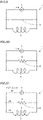
Figs. 9 to 14 , the operation of persistentcurrent switch 8 will be described. As illustrated inFigs. 1 and9 to 14 , persistentcurrent switch 8 is connected in parallel tosuperconducting coil 3.Superconducting coil 3 and persistentcurrent switch 8 are connected to acurrent source 7. -
Superconducting coil 3 and persistentcurrent switch 8 are cooled to a temperature lower than or equal to the superconducting transition temperature. Specifically, as illustrated inFig. 1 ,superconducting coil 3 and persistentcurrent switch 8 are immersed inliquid refrigerant 6. The current does not flow throughheater 21, andheater 21 is in an off state.Superconducting layer 13 included in persistentcurrent switch 8 transitions to the superconducting state. As illustrated inFig. 9 , persistentcurrent switch 8 has zero electrical resistance. Persistentcurrent switch 8 is turned on.Superconducting coil 3 also transitions to the superconducting state. A current I flowing fromcurrent source 7 is zero. - Then, the current is applied to
heater 21 to turn on heater 21 (heat generation state). A part of superconducting wire 10 (superconducting layer 13) transitions to the normal conducting state. As illustrated inFig. 10 , the electric resistance of persistentcurrent switch 8 is greater than zero, and persistentcurrent switch 8 has an off-resistance R. Persistentcurrent switch 8 is turned off. Current I flowing fromcurrent source 7 is still zero. - Then, as illustrated in
Fig. 11 , current I starts to flow fromcurrent source 7. Current I flowing fromcurrent source 7 is gradually increased from zero with a time change ΔI/Δt of currentI. Superconducting coil 3 has inductance L. When current I flowing fromcurrent source 7 is gradually increased, coil impedance Z corresponding to time change ΔI/Δt of current I is generated insuperconducting coil 3. An increased current from zero of current I flowing fromcurrent source 7 flows to persistentcurrent switch 8 andsuperconducting coil 3 according to off-resistance R of persistentcurrent switch 8 and coil impedance Z ofsuperconducting coil 3. This increasing current is given by time integral ΣΔI/Δt of time change ΔI/Δt of current I. - As illustrated in
Fig. 12 , when current I flowing fromcurrent source 7 reaches an operating current I0 flowing tosuperconducting coil 3 in a persistent current mode, current I flowing fromcurrent source 7 is maintained at operating current I0. Time change ΔI/Δt of current I flowing fromcurrent source 7 becomes zero, and coil impedance Z ofsuperconducting coil 3 also becomes zero. On the other hand, persistentcurrent switch 8 still has off-resistance R larger than zero. For this reason, the current flowing through persistentcurrent switch 8 gradually decreases, and the current flowing throughsuperconducting coil 3 gradually increases. Operating current I0 flowing fromcurrent source 7 flows exclusively tosuperconducting coil 3. In this way,superconducting coil 3 is excited. - The flow of the current through
heater 21 is stopped, andheater 21 is turned off.Liquid refrigerant 6 absorbs residual heat ofheater 21. A part of superconducting wire 10 (superconducting layer 13) in the normal conducting state transitions to the superconducting state. As illustrated inFig. 13 , the electric resistance of persistentcurrent switch 8 becomes zero. Persistentcurrent switch 8 is turned on. - Then, as illustrated in
Fig. 13 , current I flowing fromcurrent source 7 is gradually decreased from operating current I0 at time change -ΔI/Δt of current I. A decreasing current from operating current I0 of current I flowing fromcurrent source 7 flows to persistentcurrent switch 8. This decreasing current is given by time integral -ΣΔI/Δt of time change -ΔI/Δt of current I. As illustrated inFig. 14 , when the current flowing fromcurrent source 7 is set to zero, operating current I0 circulates through persistentcurrent switch 8 andsuperconducting coil 3. In this way, persistentcurrent switch 8 can operatesuperconducting device 1 in the persistent current mode. - With reference to
Fig. 15 , action of persistentcurrent switch 8 of the first embodiment will be described while being compared with a persistent current switch of a comparative example. The persistent current switch of the comparative example has the same configuration as persistentcurrent switch 8 of the first embodiment, but is different in thatheater 21 and insulatingmember 22 are disposed on the side of firstprincipal surface 13m ofsuperconducting layer 13. Specifically, in the comparative example,heater 21 and insulatingmember 22 are provided on a second surface ofsubstrate 11 on the opposite side of a first surface ofsubstrate 11 facing the first principal surface ofsuperconducting layer 13. In the comparative example, insulatingmember 22 is disposed between the second surface ofsubstrate 11 andheater 21. - It can be seen from
Fig. 15 that persistentcurrent switch 8 of the first embodiment operates with lower power consumption than the persistent current switch of the comparative example. The reason is as follows. In persistentcurrent switch 8 of the first embodiment,heater 21 is disposed only on the side of secondprincipal surface 13n ofsuperconducting layer 13 with respect tosuperconducting layer 13. Accordingly, in the first embodiment, the heat dissipated tosubstrate 11 in the heat generated byheater 21 is reduced as compared with the comparative example.Superconducting layer 13 in persistentcurrent switch 8 of the first embodiment can be more efficiently heated byheater 21 thansuperconducting layer 13 in the persistent current switch of the comparative example. Off-resistance R of persistentcurrent switch 8 increases with less power consumption ofheater 21. - In general, the larger off-resistance R of persistent
current switch 8, the shorter the time required to operatesuperconducting device 1 in the persistent current mode. Accordingly, persistentcurrent switch 8 of the first embodiment can operatesuperconducting device 1 in the persistent current mode in a shorter time than the persistent current switch of the comparative example. - Effects of persistent
current switch 8 andsuperconducting device 1 of the first embodiment will be described. - Persistent
current switch 8 includessuperconducting wire 10,heater 21, and insulatingmember 22.Superconducting wire 10 includessubstrate 11 andsuperconducting layer 13 provided onsubstrate 11.Superconducting layer 13 includes firstprincipal surface 13m facing substrate 11 and secondprincipal surface 13n on the opposite side of firstprincipal surface 13m.Heater 21 is disposed only on the side of secondprincipal surface 13n ofsuperconducting layer 13 with respect tosuperconducting layer 13. Insulatingmember 22 is provided between secondprincipal surface 13n ofsuperconducting layer 13 andheater 21. -
Heater 21 is disposed only on the side of secondprincipal surface 13n ofsuperconducting layer 13 with respect tosuperconducting layer 13. The heat dissipated tosubstrate 11 in the heat generated byheater 21 is reduced.Superconducting layer 13 can be efficiently heated byheater 21. In addition, because insulatingmember 22 is provided between secondprincipal surface 13n ofsuperconducting layer 13 andheater 21, insulatingmember 22 prevents the current flowing throughheater 21 from flowing intosuperconducting layer 13. For this reason, the power consumption ofheater 21 required for operating persistentcurrent switch 8 is reduced. Persistentcurrent switch 8 can operate at lower power consumption. -
Superconducting device 1 includes persistentcurrent switch 8,superconducting coil 3 connected to persistentcurrent switch 8, andcontainer 5 that accommodates persistentcurrent switch 8 andsuperconducting coil 3. Accordingly,superconducting device 1 can operate with lower power consumption.Superconducting device 1 can operate in the persistent current mode in a shorter time. - With reference to
Fig. 16 , a persistentcurrent switch 8b will be described. Persistentcurrent switch 8b of a second embodiment has the same configuration as persistentcurrent switch 8 of the first embodiment, but is mainly different in the following points. -
Superconducting wire 10 further includes astabilization layer 15 having conductivity. For example,stabilization layer 15 is formed of a metal such as copper (Cu) or an alloy.Stabilization layer 15 is in contact withprotective layer 14. For example,stabilization layer 15 has a larger thickness thanprotective layer 14.Protective layer 14 is provided between secondprincipal surface 13n ofsuperconducting layer 13 andstabilization layer 15.Stabilization layer 15 is provided between insulatingmember 22 andprotective layer 14. Insulatingmember 22 is provided betweenstabilization layer 15 andheater 21.Heater 21 is separated fromstabilization layer 15.Stabilization layer 15 covers an entire outer periphery of a laminated body including, for example,substrate 11,intermediate layer 12,superconducting layer 13, andprotective layer 14. When the quenching (the phenomenon of transition from the superconducting state to the normal conducting state) occurs insuperconducting layer 13,stabilization layer 15 bypasses the current flowing throughsuperconducting layer 13 to prevent the burning of thesuperconducting wire 10. - As illustrated in
Fig. 1 ,superconducting device 1 of the second embodiment includes persistentcurrent switch 8b of the second embodiment instead of persistentcurrent switch 8 of the first embodiment. - With reference to
Figs. 17 to 20 , a persistentcurrent switch 8c will be described. Persistentcurrent switch 8c of a third embodiment has the same configuration as persistentcurrent switch 8 of the first embodiment, but is mainly different in the following points. -
Superconducting layer 13 includes afirst portion 13a, asecond portion 13b, and athird portion 13c between thefirst portion 13a and thesecond portion 13b along the longitudinal direction ofsuperconducting wire 10.Protective layer 14 is provided only onfirst portion 13a andsecond portion 13b.Protective layer 14 is not formed onthird portion 13c, andthird portion 13c ofsuperconducting layer 13 is exposed fromprotective layer 14.Protective layer 14 formed onfirst portion 13a andprotective layer 14 formed onsecond portion 13b are separated from each other in the longitudinal direction ofsuperconducting wire 10 atthird portion 13c. -
Heater 21 is provided only onthird portion 13c. Insulatingmember 22 is provided betweenheater 21 andthird portion 13c.Heater 21 is not provided onfirst portion 13a andsecond portion 13b.Heater 21 is separated fromprotective layer 14 formed onfirst portion 13a andsecond portion 13b. - In a modification of the third embodiment,
stabilization layer 15 is provided onprotective layer 14 similarly to the second embodiment. - As illustrated in
Fig. 1 ,superconducting device 1 of the third embodiment includes persistentcurrent switch 8c of the third embodiment or a modification of the third embodiment instead of persistentcurrent switch 8 of the first embodiment. - The third embodiment has the following effects in addition to the effects of the first embodiment.
-
Protective layer 14 is provided only onfirst portion 13a andsecond portion 13b, but is not provided onthird portion 13c. For this reason, the current flowing throughsuperconducting wire 10 cannot bypassthird portion 13c. Whenthird portion 13c is heated byheater 21 to be in the normal conducting state, all the current flowing throughsuperconducting wire 10 flows throughthird portion 13c having high electric resistance. Even when the heating length or heating area ofsuperconducting layer 13 usingheater 21 is smaller, high off-resistance R of persistentcurrent switch 8c can be obtained. The power consumption ofheater 21 required for operating persistentcurrent switch 8 c is reduced. Persistentcurrent switch 8c may operate with less power consumption. -
Heater 21 is provided only onthird portion 13c exposed fromprotective layer 14, and is separated fromprotective layer 14. Accordingly, the current flowing throughheater 21 is prevented from flowing intoprotective layer 14. The power consumption of the heater required for operating persistentcurrent switch 8c is reduced. Persistentcurrent switch 8c can operate with less power consumption ofheater 21. - With reference to
Fig. 21 , a persistentcurrent switch 8d will be described. Persistentcurrent switch 8d of a fourth embodiment has the same configuration as persistentcurrent switch 8 of the first embodiment, but is mainly different in the following points. In persistentcurrent switch 8d, in plan view of secondprincipal surface 13n ofsuperconducting layer 13, athird side edge 13s ofsuperconducting layer 13 and afirst side edge 14s ofprotective layer 14 are located inside asecond side edge 12s ofintermediate layer 12. - When superconducting member 17 (see
Figs. 7 and 8 ) is divided, sometimes the side edge ofsubstrate 11 orfirst side edge 14s ofprotective layer 14 deforms andsuperconducting layer 13 orprotective layer 14 comes into contact withsubstrate 11. In particular, whensubstrate 11 includes a layer (second layer 11b) made of relatively soft copper, and when superconductingmember 17 is divided by a machine slit, there is a concern thatsuperconducting layer 13 orprotective layer 14 comes into contact withsubstrate 11. When superconductinglayer 13 orprotective layer 14 comes into contact withsubstrate 11, the heat generated byheater 21 is dissipated tosubstrate 11 to increase the power consumption of the persistent current switch. - On the other hand, in persistent
current switch 8d,third side edge 13s ofsuperconducting layer 13 andfirst side edge 14s ofprotective layer 14 are located insidesecond side edge 12s ofintermediate layer 12. For this reason, even whensubstrate 11 orprotective layer 14 deforms with respect to the machine slit ofsuperconducting member 17,superconducting layer 13 andprotective layer 14 are not in contact withsubstrate 11 and remain separated fromsubstrate 11. The heat dissipation fromheater 21 tosubstrate 11 throughsuperconducting layer 13 orprotective layer 14 can be reduced. Persistentcurrent switch 8d can operate with lower power consumption. - Referring to
Fig. 22 , in a persistentcurrent switch 8e of a first modification of the fourth embodiment, insuperconducting wire 10,first side edge 14s ofprotective layer 14 is located insidesecond side edge 12s ofintermediate layer 12 in plan view of secondprincipal surface 13n ofsuperconducting layer 13. - When superconducting member 17 (see
Figs. 7 and 8 ) is divided, sometimes the side edge ofsubstrate 11 orfirst side edge 14s ofprotective layer 14 deforms andprotective layer 14 comes into contact withsubstrate 11. In particular, whensubstrate 11 includes the layer (second layer 11b) made of relatively soft copper, andsuperconducting member 17 is divided by the machine slit, there is a concern thatprotective layer 14 comes into contact withsubstrate 11. Whenprotective layer 14 comes into contact withsubstrate 11, the heat generated byheater 21 is dissipated tosubstrate 11 to increase the power consumption of the persistent current switch. - On the other hand, in persistent
current switch 8e,first side edge 14s ofprotective layer 14 is located insidesecond side edge 12s ofintermediate layer 12. For this reason, even whensubstrate 11 orprotective layer 14 deforms with respect to the machine slit ofsuperconducting member 17,protective layer 14 is not in contact withsubstrate 11 and remains separated fromsubstrate 11. The heat dissipation fromheater 21 tosubstrate 11 throughprotective layer 14 can be reduced. Persistentcurrent switch 8e can operate with lower power consumption. - In a second modification of the fourth embodiment, in
superconducting wire 10 of the second embodiment orsuperconducting wire 10 of the third embodiment, like persistentcurrent switch 8d of the fourth embodiment,third side edge 13s ofsuperconducting layer 13 andfirst side edge 14s ofprotective layer 14 are located insidesecond side edge 12s ofintermediate layer 12. In a third modification of the fourth embodiment, insuperconducting wire 10 of the second embodiment orsuperconducting wire 10 of the third embodiment, like the persistentcurrent switch 8e of the first modification of the fourth embodiment,first side edge 14s ofprotective layer 14 is located insidesecond side edge 12s ofintermediate layer 12. - As illustrated in
Fig. 1 ,superconducting device 1 of the fourth embodiment includes any one of persistentcurrent switches current switch 8 of the first embodiment. - It should be understood that the first to fourth embodiments disclosed herein are illustrative in all respects and are not restrictive. The scope of the present invention is defined not by the first to fourth embodiments but by the claims, and is intended to include meanings equivalent to the claims and all modifications within the scope.
- 1: superconducting device, 3: superconducting coil, 5: container, 6: liquid refrigerant, 7: current source, 8, 8b, 8c, 8d, 8e: persistent current switch, 10: superconducting wire, 11: substrate, 11a: first layer, 11b: second layer, 11c: third layer, 12: intermediate layer, 12s: second side edge, 13: superconducting layer, 13a: first portion, 13b: second portion, 13c: third portion, 13m: first principal surface, 13n: second principal surface, 13s: third side edge, 14: protective layer, 14s: first side edge, 15: stabilization layer, 17: superconducting member, 21: heater, 22: insulating member, 30: holding member
Claims (13)
- A persistent current switch comprising:a superconducting wire;a heater; andan insulating member,wherein the superconducting wire includes a substrate and a superconducting layer provided on the substrate,the superconducting layer includes a first principal surface facing the substrate and a second principal surface on an opposite side of the first principal surface,the heater is disposed only on a side of the second principal surface with respect to the superconducting layer, andthe insulating member is provided between the second principal surface and the heater.
- The persistent current switch according to claim 1, wherein the superconducting wire further includes a protective layer having conductivity,the protective layer is provided on the second principal surface of the superconducting layer and is in contact with the superconducting layer, andthe insulating member is provided between the protective layer and the heater.
- The persistent current switch according to claim 2, wherein the protective layer and the superconducting layer are separated from the substrate.
- The persistent current switch according to claim 1, wherein the superconducting wire further includes a protective layer having conductivity,the protective layer is provided on the second principal surface of the superconducting layer and is in contact with the superconducting layer,the superconducting layer includes a first portion, a second portion, and a third portion located between the first portion and the second portion along a longitudinal direction of the superconducting wire,the protective layer is provided only on the first portion and the second portion,the heater is provided only on the third portion and is separated from the protective layer, andthe insulating member is provided between the heater and the third portion.
- The persistent current switch according to any one of claims 2 to 4, wherein the superconducting wire further includes a stabilization layer having conductivity,the stabilization layer is in contact with the protective layer,the protective layer is provided between the superconducting layer and the stabilization layer, andthe heater is separated from the stabilization layer.
- The persistent current switch according to any one of claims 1 to 5, wherein the superconducting wire further includes an intermediate layer having an insulating property, and
the intermediate layer is provided between the substrate and the first principal surface. - The persistent current switch according to any one of claims 2 to 5, wherein the superconducting wire further includes an intermediate layer having an insulating property,the intermediate layer is provided between the substrate and the first principal surface, anda first side edge of the protective layer is located inside a second side edge of the intermediate layer in plan view of the second principal surface.
- The persistent current switch according to claim 7, wherein a third side edge of the superconducting layer is located inside the second side edge of the intermediate layer in plan view of the second principal surface.
- The persistent current switch according to any one of claims 1 to 8, wherein the superconducting wire has a non-coil shape.
- The persistent current switch according to any one of claims 1 to 9, further comprising a holding member,wherein a held portion of the superconducting wire is held by the holding member, andthe heater is provided only on a part of the held portion.
- The persistent current switch according to claim 10, wherein the heater is provided over a length less than or equal to 50% of a length of the held portion in a longitudinal direction of the superconducting wire.
- The persistent current switch according to any one of claims 1 to 11, wherein the superconducting layer is formed of RE1Ba2Cu3Oy, where y is greater than or equal to 6.0 and less than or equal to 8.0, and RE represents a rare earth element.
- A superconducting device comprising:the persistent current switch according to any one of claims 1 to 12;a superconducting coil connected to the persistent current switch; anda container that accommodates the persistent current switch and the superconducting coil.
Applications Claiming Priority (2)
| Application Number | Priority Date | Filing Date | Title |
|---|---|---|---|
| JP2019171570 | 2019-09-20 | ||
| PCT/JP2020/025063 WO2021053921A1 (en) | 2019-09-20 | 2020-06-25 | Permanent current switch and superconducting device |
Publications (3)
| Publication Number | Publication Date |
|---|---|
| EP4033551A1 true EP4033551A1 (en) | 2022-07-27 |
| EP4033551A4 EP4033551A4 (en) | 2022-11-23 |
| EP4033551B1 EP4033551B1 (en) | 2024-05-22 |
Family
ID=74884029
Family Applications (1)
| Application Number | Title | Priority Date | Filing Date |
|---|---|---|---|
| EP20865413.7A Active EP4033551B1 (en) | 2019-09-20 | 2020-06-25 | Permanent current switch and superconducting device |
Country Status (4)
| Country | Link |
|---|---|
| US (1) | US20220393680A1 (en) |
| EP (1) | EP4033551B1 (en) |
| JP (1) | JP7452547B2 (en) |
| WO (1) | WO2021053921A1 (en) |
Family Cites Families (12)
| Publication number | Priority date | Publication date | Assignee | Title |
|---|---|---|---|---|
| US4841268A (en) * | 1987-09-28 | 1989-06-20 | General Atomics | MRI Magnet system with permanently installed power leads |
| US5410288A (en) * | 1993-01-04 | 1995-04-25 | General Electric Company | Persistent superconducting switch for a superconducting magnet for imaging human limbs |
| JP2003069093A (en) * | 2001-08-29 | 2003-03-07 | Central Japan Railway Co | Permanent current switch and superconducting magnet using the same |
| JP5386550B2 (en) * | 2011-07-05 | 2014-01-15 | 株式会社日立製作所 | Superconducting switch, superconducting magnet, and MRI |
| KR101374177B1 (en) * | 2012-10-11 | 2014-03-14 | 케이조인스(주) | Methods of splicing 2g rebco high temperature superconductors using partial micro-melting diffusion pressurized splicing by direct face-to-face contact of high temperature superconducting layers and recovering superconductivity by oxygenation annealing |
| JP6163348B2 (en) * | 2013-04-24 | 2017-07-12 | 株式会社フジクラ | Operating method of high temperature superconducting coil |
| DE102013214447B3 (en) * | 2013-07-24 | 2014-11-20 | Bruker Hts Gmbh | Band-shaped, superconducting element with improved self-protection in quenching |
| JP6666274B2 (en) | 2017-01-18 | 2020-03-13 | 株式会社東芝 | High temperature superconducting permanent current switch and high temperature superconducting magnet device |
| US11287171B1 (en) * | 2017-07-05 | 2022-03-29 | Rigetti & Co, Llc | Heat switches for controlling a flow of heat between thermal stages of a cryostat |
| JP7040730B2 (en) * | 2017-11-28 | 2022-03-23 | 東海旅客鉄道株式会社 | Permanent current switch |
| JP7060412B2 (en) * | 2018-03-07 | 2022-04-26 | 古河電気工業株式会社 | Permanent current switch and superconducting magnet device |
| JP2019171570A (en) | 2018-03-26 | 2019-10-10 | 京セラドキュメントソリューションズ株式会社 | Image formation apparatus |
-
2020
- 2020-06-25 WO PCT/JP2020/025063 patent/WO2021053921A1/en not_active Ceased
- 2020-06-25 EP EP20865413.7A patent/EP4033551B1/en active Active
- 2020-06-25 JP JP2021546512A patent/JP7452547B2/en active Active
- 2020-06-25 US US17/642,804 patent/US20220393680A1/en not_active Abandoned
Also Published As
| Publication number | Publication date |
|---|---|
| WO2021053921A1 (en) | 2021-03-25 |
| EP4033551B1 (en) | 2024-05-22 |
| JPWO2021053921A1 (en) | 2021-03-25 |
| US20220393680A1 (en) | 2022-12-08 |
| EP4033551A4 (en) | 2022-11-23 |
| JP7452547B2 (en) | 2024-03-19 |
Similar Documents
| Publication | Publication Date | Title |
|---|---|---|
| US20110218111A1 (en) | High temperature superconducting parallel conductors, high temperature superconducting coil using the same, and high temperature superconducting magnet | |
| ES2938711T3 (en) | High Temperature Superconducting Magnet | |
| KR102562414B1 (en) | Superconducting wire and superconducting coil | |
| JP6680828B2 (en) | Flexible superconducting lead wire assembly | |
| WO2021195330A1 (en) | Passive quench protection techniques for non-insulated superconducting magnets | |
| KR20150065694A (en) | Superconductive coil device and production method | |
| JP5022279B2 (en) | Oxide superconducting current lead | |
| JP6035050B2 (en) | Superconducting coil device and manufacturing method thereof | |
| EP4033551B1 (en) | Permanent current switch and superconducting device | |
| JP7279723B2 (en) | Superconducting wire and persistent current switch | |
| WO2022168483A1 (en) | Superconducting magnet apparatus, magnetic resonance imaging apparatus, and method for demagnetizing superconducting magnet | |
| JP2019096849A (en) | Permanent current switch | |
| US20020132738A1 (en) | Power lead for superconductive magnet | |
| JP6862382B2 (en) | High-temperature superconducting magnet device, its operation control device and method | |
| JP5882402B2 (en) | Superconducting current lead | |
| JP2012059468A (en) | Superconductive current lead | |
| JP2012064323A (en) | Superconductive current lead | |
| JP2004335160A (en) | Current leads for superconducting devices | |
| JP6238623B2 (en) | Superconducting current lead | |
| JP5925827B2 (en) | Superconducting current lead | |
| JP2018055990A (en) | Superconductive current lead and oxide superconducting wire material | |
| JP6327794B2 (en) | Superconducting coil device | |
| EP4113548A1 (en) | Superconducting magnet, superconducting wire, and method for producing superconducting magnet | |
| JPH10247532A (en) | Current leads for superconducting devices | |
| JP2021166126A (en) | Superconducting current lead |
Legal Events
| Date | Code | Title | Description |
|---|---|---|---|
| STAA | Information on the status of an ep patent application or granted ep patent |
Free format text: STATUS: THE INTERNATIONAL PUBLICATION HAS BEEN MADE |
|
| PUAI | Public reference made under article 153(3) epc to a published international application that has entered the european phase |
Free format text: ORIGINAL CODE: 0009012 |
|
| STAA | Information on the status of an ep patent application or granted ep patent |
Free format text: STATUS: REQUEST FOR EXAMINATION WAS MADE |
|
| 17P | Request for examination filed |
Effective date: 20220317 |
|
| AK | Designated contracting states |
Kind code of ref document: A1 Designated state(s): AL AT BE BG CH CY CZ DE DK EE ES FI FR GB GR HR HU IE IS IT LI LT LU LV MC MK MT NL NO PL PT RO RS SE SI SK SM TR |
|
| A4 | Supplementary search report drawn up and despatched |
Effective date: 20221025 |
|
| RIC1 | Information provided on ipc code assigned before grant |
Ipc: H01B 12/06 20060101ALI20221020BHEP Ipc: H01F 6/06 20060101ALI20221020BHEP Ipc: H01L 39/14 20060101ALI20221020BHEP Ipc: H01L 39/16 20060101AFI20221020BHEP |
|
| DAV | Request for validation of the european patent (deleted) | ||
| DAX | Request for extension of the european patent (deleted) | ||
| REG | Reference to a national code |
Ref country code: DE Ref legal event code: R079 Free format text: PREVIOUS MAIN CLASS: H01L0039160000 Ipc: H01F0006060000 Ref country code: DE Ref legal event code: R079 Ref document number: 602020031434 Country of ref document: DE Free format text: PREVIOUS MAIN CLASS: H01L0039160000 Ipc: H01F0006060000 |
|
| RIC1 | Information provided on ipc code assigned before grant |
Ipc: H10N 60/355 20230101ALI20231106BHEP Ipc: H01B 12/06 20060101ALI20231106BHEP Ipc: H01F 6/06 20060101AFI20231106BHEP |
|
| GRAP | Despatch of communication of intention to grant a patent |
Free format text: ORIGINAL CODE: EPIDOSNIGR1 |
|
| STAA | Information on the status of an ep patent application or granted ep patent |
Free format text: STATUS: GRANT OF PATENT IS INTENDED |
|
| INTG | Intention to grant announced |
Effective date: 20240108 |
|
| GRAS | Grant fee paid |
Free format text: ORIGINAL CODE: EPIDOSNIGR3 |
|
| GRAA | (expected) grant |
Free format text: ORIGINAL CODE: 0009210 |
|
| STAA | Information on the status of an ep patent application or granted ep patent |
Free format text: STATUS: THE PATENT HAS BEEN GRANTED |
|
| AK | Designated contracting states |
Kind code of ref document: B1 Designated state(s): AL AT BE BG CH CY CZ DE DK EE ES FI FR GB GR HR HU IE IS IT LI LT LU LV MC MK MT NL NO PL PT RO RS SE SI SK SM TR |
|
| P01 | Opt-out of the competence of the unified patent court (upc) registered |
Effective date: 20240415 |
|
| REG | Reference to a national code |
Ref country code: GB Ref legal event code: FG4D |
|
| REG | Reference to a national code |
Ref country code: CH Ref legal event code: EP |
|
| REG | Reference to a national code |
Ref country code: DE Ref legal event code: R096 Ref document number: 602020031434 Country of ref document: DE |
|
| REG | Reference to a national code |
Ref country code: IE Ref legal event code: FG4D |
|
| REG | Reference to a national code |
Ref country code: LT Ref legal event code: MG9D |
|
| REG | Reference to a national code |
Ref country code: CH Ref legal event code: PK Free format text: BERICHTIGUNGEN |
|
| REG | Reference to a national code |
Ref country code: NL Ref legal event code: MP Effective date: 20240522 |
|
| PG25 | Lapsed in a contracting state [announced via postgrant information from national office to epo] |
Ref country code: IS Free format text: LAPSE BECAUSE OF FAILURE TO SUBMIT A TRANSLATION OF THE DESCRIPTION OR TO PAY THE FEE WITHIN THE PRESCRIBED TIME-LIMIT Effective date: 20240922 |
|
| PG25 | Lapsed in a contracting state [announced via postgrant information from national office to epo] |
Ref country code: BG Free format text: LAPSE BECAUSE OF FAILURE TO SUBMIT A TRANSLATION OF THE DESCRIPTION OR TO PAY THE FEE WITHIN THE PRESCRIBED TIME-LIMIT Effective date: 20240522 |
|
| PG25 | Lapsed in a contracting state [announced via postgrant information from national office to epo] |
Ref country code: FI Free format text: LAPSE BECAUSE OF FAILURE TO SUBMIT A TRANSLATION OF THE DESCRIPTION OR TO PAY THE FEE WITHIN THE PRESCRIBED TIME-LIMIT Effective date: 20240522 Ref country code: HR Free format text: LAPSE BECAUSE OF FAILURE TO SUBMIT A TRANSLATION OF THE DESCRIPTION OR TO PAY THE FEE WITHIN THE PRESCRIBED TIME-LIMIT Effective date: 20240522 |
|
| PG25 | Lapsed in a contracting state [announced via postgrant information from national office to epo] |
Ref country code: GR Free format text: LAPSE BECAUSE OF FAILURE TO SUBMIT A TRANSLATION OF THE DESCRIPTION OR TO PAY THE FEE WITHIN THE PRESCRIBED TIME-LIMIT Effective date: 20240823 |
|
| PG25 | Lapsed in a contracting state [announced via postgrant information from national office to epo] |
Ref country code: PT Free format text: LAPSE BECAUSE OF FAILURE TO SUBMIT A TRANSLATION OF THE DESCRIPTION OR TO PAY THE FEE WITHIN THE PRESCRIBED TIME-LIMIT Effective date: 20240923 |
|
| REG | Reference to a national code |
Ref country code: AT Ref legal event code: MK05 Ref document number: 1689458 Country of ref document: AT Kind code of ref document: T Effective date: 20240522 |
|
| PG25 | Lapsed in a contracting state [announced via postgrant information from national office to epo] |
Ref country code: NL Free format text: LAPSE BECAUSE OF FAILURE TO SUBMIT A TRANSLATION OF THE DESCRIPTION OR TO PAY THE FEE WITHIN THE PRESCRIBED TIME-LIMIT Effective date: 20240522 |
|
| PG25 | Lapsed in a contracting state [announced via postgrant information from national office to epo] |
Ref country code: ES Free format text: LAPSE BECAUSE OF FAILURE TO SUBMIT A TRANSLATION OF THE DESCRIPTION OR TO PAY THE FEE WITHIN THE PRESCRIBED TIME-LIMIT Effective date: 20240522 |
|
| PG25 | Lapsed in a contracting state [announced via postgrant information from national office to epo] |
Ref country code: AT Free format text: LAPSE BECAUSE OF FAILURE TO SUBMIT A TRANSLATION OF THE DESCRIPTION OR TO PAY THE FEE WITHIN THE PRESCRIBED TIME-LIMIT Effective date: 20240522 |
|
| PG25 | Lapsed in a contracting state [announced via postgrant information from national office to epo] |
Ref country code: PL Free format text: LAPSE BECAUSE OF FAILURE TO SUBMIT A TRANSLATION OF THE DESCRIPTION OR TO PAY THE FEE WITHIN THE PRESCRIBED TIME-LIMIT Effective date: 20240522 |
|
| PG25 | Lapsed in a contracting state [announced via postgrant information from national office to epo] |
Ref country code: LV Free format text: LAPSE BECAUSE OF FAILURE TO SUBMIT A TRANSLATION OF THE DESCRIPTION OR TO PAY THE FEE WITHIN THE PRESCRIBED TIME-LIMIT Effective date: 20240522 |
|
| PG25 | Lapsed in a contracting state [announced via postgrant information from national office to epo] |
Ref country code: PT Free format text: LAPSE BECAUSE OF FAILURE TO SUBMIT A TRANSLATION OF THE DESCRIPTION OR TO PAY THE FEE WITHIN THE PRESCRIBED TIME-LIMIT Effective date: 20240923 Ref country code: PL Free format text: LAPSE BECAUSE OF FAILURE TO SUBMIT A TRANSLATION OF THE DESCRIPTION OR TO PAY THE FEE WITHIN THE PRESCRIBED TIME-LIMIT Effective date: 20240522 Ref country code: NO Free format text: LAPSE BECAUSE OF FAILURE TO SUBMIT A TRANSLATION OF THE DESCRIPTION OR TO PAY THE FEE WITHIN THE PRESCRIBED TIME-LIMIT Effective date: 20240822 Ref country code: NL Free format text: LAPSE BECAUSE OF FAILURE TO SUBMIT A TRANSLATION OF THE DESCRIPTION OR TO PAY THE FEE WITHIN THE PRESCRIBED TIME-LIMIT Effective date: 20240522 Ref country code: LV Free format text: LAPSE BECAUSE OF FAILURE TO SUBMIT A TRANSLATION OF THE DESCRIPTION OR TO PAY THE FEE WITHIN THE PRESCRIBED TIME-LIMIT Effective date: 20240522 Ref country code: IS Free format text: LAPSE BECAUSE OF FAILURE TO SUBMIT A TRANSLATION OF THE DESCRIPTION OR TO PAY THE FEE WITHIN THE PRESCRIBED TIME-LIMIT Effective date: 20240922 Ref country code: HR Free format text: LAPSE BECAUSE OF FAILURE TO SUBMIT A TRANSLATION OF THE DESCRIPTION OR TO PAY THE FEE WITHIN THE PRESCRIBED TIME-LIMIT Effective date: 20240522 Ref country code: GR Free format text: LAPSE BECAUSE OF FAILURE TO SUBMIT A TRANSLATION OF THE DESCRIPTION OR TO PAY THE FEE WITHIN THE PRESCRIBED TIME-LIMIT Effective date: 20240823 Ref country code: FI Free format text: LAPSE BECAUSE OF FAILURE TO SUBMIT A TRANSLATION OF THE DESCRIPTION OR TO PAY THE FEE WITHIN THE PRESCRIBED TIME-LIMIT Effective date: 20240522 Ref country code: ES Free format text: LAPSE BECAUSE OF FAILURE TO SUBMIT A TRANSLATION OF THE DESCRIPTION OR TO PAY THE FEE WITHIN THE PRESCRIBED TIME-LIMIT Effective date: 20240522 Ref country code: BG Free format text: LAPSE BECAUSE OF FAILURE TO SUBMIT A TRANSLATION OF THE DESCRIPTION OR TO PAY THE FEE WITHIN THE PRESCRIBED TIME-LIMIT Effective date: 20240522 Ref country code: AT Free format text: LAPSE BECAUSE OF FAILURE TO SUBMIT A TRANSLATION OF THE DESCRIPTION OR TO PAY THE FEE WITHIN THE PRESCRIBED TIME-LIMIT Effective date: 20240522 Ref country code: RS Free format text: LAPSE BECAUSE OF FAILURE TO SUBMIT A TRANSLATION OF THE DESCRIPTION OR TO PAY THE FEE WITHIN THE PRESCRIBED TIME-LIMIT Effective date: 20240822 |
|
| REG | Reference to a national code |
Ref country code: DE Ref legal event code: R119 Ref document number: 602020031434 Country of ref document: DE |
|
| PG25 | Lapsed in a contracting state [announced via postgrant information from national office to epo] |
Ref country code: DK Free format text: LAPSE BECAUSE OF FAILURE TO SUBMIT A TRANSLATION OF THE DESCRIPTION OR TO PAY THE FEE WITHIN THE PRESCRIBED TIME-LIMIT Effective date: 20240522 |
|
| PG25 | Lapsed in a contracting state [announced via postgrant information from national office to epo] |
Ref country code: EE Free format text: LAPSE BECAUSE OF FAILURE TO SUBMIT A TRANSLATION OF THE DESCRIPTION OR TO PAY THE FEE WITHIN THE PRESCRIBED TIME-LIMIT Effective date: 20240522 |
|
| PG25 | Lapsed in a contracting state [announced via postgrant information from national office to epo] |
Ref country code: CZ Free format text: LAPSE BECAUSE OF FAILURE TO SUBMIT A TRANSLATION OF THE DESCRIPTION OR TO PAY THE FEE WITHIN THE PRESCRIBED TIME-LIMIT Effective date: 20240522 |
|
| PG25 | Lapsed in a contracting state [announced via postgrant information from national office to epo] |
Ref country code: SK Free format text: LAPSE BECAUSE OF FAILURE TO SUBMIT A TRANSLATION OF THE DESCRIPTION OR TO PAY THE FEE WITHIN THE PRESCRIBED TIME-LIMIT Effective date: 20240522 Ref country code: RO Free format text: LAPSE BECAUSE OF FAILURE TO SUBMIT A TRANSLATION OF THE DESCRIPTION OR TO PAY THE FEE WITHIN THE PRESCRIBED TIME-LIMIT Effective date: 20240522 |
|
| PG25 | Lapsed in a contracting state [announced via postgrant information from national office to epo] |
Ref country code: SK Free format text: LAPSE BECAUSE OF FAILURE TO SUBMIT A TRANSLATION OF THE DESCRIPTION OR TO PAY THE FEE WITHIN THE PRESCRIBED TIME-LIMIT Effective date: 20240522 Ref country code: RO Free format text: LAPSE BECAUSE OF FAILURE TO SUBMIT A TRANSLATION OF THE DESCRIPTION OR TO PAY THE FEE WITHIN THE PRESCRIBED TIME-LIMIT Effective date: 20240522 Ref country code: EE Free format text: LAPSE BECAUSE OF FAILURE TO SUBMIT A TRANSLATION OF THE DESCRIPTION OR TO PAY THE FEE WITHIN THE PRESCRIBED TIME-LIMIT Effective date: 20240522 Ref country code: DK Free format text: LAPSE BECAUSE OF FAILURE TO SUBMIT A TRANSLATION OF THE DESCRIPTION OR TO PAY THE FEE WITHIN THE PRESCRIBED TIME-LIMIT Effective date: 20240522 Ref country code: CZ Free format text: LAPSE BECAUSE OF FAILURE TO SUBMIT A TRANSLATION OF THE DESCRIPTION OR TO PAY THE FEE WITHIN THE PRESCRIBED TIME-LIMIT Effective date: 20240522 |
|
| PG25 | Lapsed in a contracting state [announced via postgrant information from national office to epo] |
Ref country code: IT Free format text: LAPSE BECAUSE OF FAILURE TO SUBMIT A TRANSLATION OF THE DESCRIPTION OR TO PAY THE FEE WITHIN THE PRESCRIBED TIME-LIMIT Effective date: 20240522 Ref country code: MC Free format text: LAPSE BECAUSE OF FAILURE TO SUBMIT A TRANSLATION OF THE DESCRIPTION OR TO PAY THE FEE WITHIN THE PRESCRIBED TIME-LIMIT Effective date: 20240522 |
|
| PG25 | Lapsed in a contracting state [announced via postgrant information from national office to epo] |
Ref country code: LU Free format text: LAPSE BECAUSE OF NON-PAYMENT OF DUE FEES Effective date: 20240625 |
|
| PLBE | No opposition filed within time limit |
Free format text: ORIGINAL CODE: 0009261 |
|
| STAA | Information on the status of an ep patent application or granted ep patent |
Free format text: STATUS: NO OPPOSITION FILED WITHIN TIME LIMIT |
|
| PG25 | Lapsed in a contracting state [announced via postgrant information from national office to epo] |
Ref country code: DE Free format text: LAPSE BECAUSE OF NON-PAYMENT OF DUE FEES Effective date: 20250101 |
|
| PG25 | Lapsed in a contracting state [announced via postgrant information from national office to epo] |
Ref country code: IE Free format text: LAPSE BECAUSE OF NON-PAYMENT OF DUE FEES Effective date: 20240625 |
|
| GBPC | Gb: european patent ceased through non-payment of renewal fee |
Effective date: 20240822 |
|
| PG25 | Lapsed in a contracting state [announced via postgrant information from national office to epo] |
Ref country code: BE Free format text: LAPSE BECAUSE OF NON-PAYMENT OF DUE FEES Effective date: 20240630 Ref country code: SI Free format text: LAPSE BECAUSE OF FAILURE TO SUBMIT A TRANSLATION OF THE DESCRIPTION OR TO PAY THE FEE WITHIN THE PRESCRIBED TIME-LIMIT Effective date: 20240522 |
|
| PG25 | Lapsed in a contracting state [announced via postgrant information from national office to epo] |
Ref country code: FR Free format text: LAPSE BECAUSE OF NON-PAYMENT OF DUE FEES Effective date: 20240722 |
|
| 26N | No opposition filed |
Effective date: 20250225 |
|
| REG | Reference to a national code |
Ref country code: BE Ref legal event code: MM Effective date: 20240630 |
|
| PG25 | Lapsed in a contracting state [announced via postgrant information from national office to epo] |
Ref country code: GB Free format text: LAPSE BECAUSE OF NON-PAYMENT OF DUE FEES Effective date: 20240822 |
|
| PG25 | Lapsed in a contracting state [announced via postgrant information from national office to epo] |
Ref country code: SE Free format text: LAPSE BECAUSE OF FAILURE TO SUBMIT A TRANSLATION OF THE DESCRIPTION OR TO PAY THE FEE WITHIN THE PRESCRIBED TIME-LIMIT Effective date: 20240522 |
|
| PG25 | Lapsed in a contracting state [announced via postgrant information from national office to epo] |
Ref country code: SM Free format text: LAPSE BECAUSE OF FAILURE TO SUBMIT A TRANSLATION OF THE DESCRIPTION OR TO PAY THE FEE WITHIN THE PRESCRIBED TIME-LIMIT; INVALID AB INITIO Effective date: 20200625 |
|
| PGFP | Annual fee paid to national office [announced via postgrant information from national office to epo] |
Ref country code: CH Payment date: 20250701 Year of fee payment: 6 |
|
| PG25 | Lapsed in a contracting state [announced via postgrant information from national office to epo] |
Ref country code: CY Free format text: LAPSE BECAUSE OF FAILURE TO SUBMIT A TRANSLATION OF THE DESCRIPTION OR TO PAY THE FEE WITHIN THE PRESCRIBED TIME-LIMIT; INVALID AB INITIO Effective date: 20200625 |
|
| PG25 | Lapsed in a contracting state [announced via postgrant information from national office to epo] |
Ref country code: HU Free format text: LAPSE BECAUSE OF FAILURE TO SUBMIT A TRANSLATION OF THE DESCRIPTION OR TO PAY THE FEE WITHIN THE PRESCRIBED TIME-LIMIT; INVALID AB INITIO Effective date: 20200625 |