EP4033531B1 - Method for manufacturing a plurality of crystalline semiconductor islands - Google Patents
Method for manufacturing a plurality of crystalline semiconductor islands Download PDFInfo
- Publication number
- EP4033531B1 EP4033531B1 EP22161925.7A EP22161925A EP4033531B1 EP 4033531 B1 EP4033531 B1 EP 4033531B1 EP 22161925 A EP22161925 A EP 22161925A EP 4033531 B1 EP4033531 B1 EP 4033531B1
- Authority
- EP
- European Patent Office
- Prior art keywords
- islands
- layer
- group
- relaxation
- substrate
- Prior art date
- Legal status (The legal status is an assumption and is not a legal conclusion. Google has not performed a legal analysis and makes no representation as to the accuracy of the status listed.)
- Active
Links
- 238000004519 manufacturing process Methods 0.000 title claims description 58
- 238000000034 method Methods 0.000 title claims description 54
- 239000004065 semiconductor Substances 0.000 title claims description 24
- 239000000758 substrate Substances 0.000 claims description 147
- 229910052738 indium Inorganic materials 0.000 claims description 26
- APFVFJFRJDLVQX-UHFFFAOYSA-N indium atom Chemical group [In] APFVFJFRJDLVQX-UHFFFAOYSA-N 0.000 claims description 26
- 230000005693 optoelectronics Effects 0.000 claims description 15
- 239000001963 growth medium Substances 0.000 claims description 12
- 239000007789 gas Substances 0.000 claims description 9
- 239000002243 precursor Substances 0.000 claims description 9
- QGZKDVFQNNGYKY-UHFFFAOYSA-N Ammonia Chemical compound N QGZKDVFQNNGYKY-UHFFFAOYSA-N 0.000 claims description 8
- 239000000203 mixture Substances 0.000 claims description 4
- 229910021529 ammonia Inorganic materials 0.000 claims description 2
- 239000010410 layer Substances 0.000 description 275
- VYPSYNLAJGMNEJ-UHFFFAOYSA-N Silicium dioxide Chemical compound O=[Si]=O VYPSYNLAJGMNEJ-UHFFFAOYSA-N 0.000 description 36
- 238000011282 treatment Methods 0.000 description 33
- 239000000463 material Substances 0.000 description 32
- 230000035882 stress Effects 0.000 description 28
- 238000010438 heat treatment Methods 0.000 description 23
- 229910002601 GaN Inorganic materials 0.000 description 19
- 238000012546 transfer Methods 0.000 description 19
- 230000015572 biosynthetic process Effects 0.000 description 17
- 230000008569 process Effects 0.000 description 16
- 235000012239 silicon dioxide Nutrition 0.000 description 16
- 239000000377 silicon dioxide Substances 0.000 description 16
- 230000005855 radiation Effects 0.000 description 15
- 229910052594 sapphire Inorganic materials 0.000 description 15
- 239000010980 sapphire Substances 0.000 description 15
- 239000011159 matrix material Substances 0.000 description 13
- 238000005516 engineering process Methods 0.000 description 12
- OAICVXFJPJFONN-UHFFFAOYSA-N Phosphorus Chemical compound [P] OAICVXFJPJFONN-UHFFFAOYSA-N 0.000 description 10
- 229910052581 Si3N4 Inorganic materials 0.000 description 10
- 238000005530 etching Methods 0.000 description 10
- HQVNEWCFYHHQES-UHFFFAOYSA-N silicon nitride Chemical compound N12[Si]34N5[Si]62N3[Si]51N64 HQVNEWCFYHHQES-UHFFFAOYSA-N 0.000 description 10
- 229910052698 phosphorus Inorganic materials 0.000 description 9
- 239000011574 phosphorus Substances 0.000 description 9
- ZOXJGFHDIHLPTG-UHFFFAOYSA-N Boron Chemical compound [B] ZOXJGFHDIHLPTG-UHFFFAOYSA-N 0.000 description 8
- 229910052796 boron Inorganic materials 0.000 description 8
- 239000005380 borophosphosilicate glass Substances 0.000 description 7
- 230000001747 exhibiting effect Effects 0.000 description 7
- 150000004767 nitrides Chemical class 0.000 description 7
- 239000003351 stiffener Substances 0.000 description 7
- 238000000151 deposition Methods 0.000 description 6
- 230000008021 deposition Effects 0.000 description 6
- 238000009826 distribution Methods 0.000 description 6
- 230000000873 masking effect Effects 0.000 description 6
- XUIMIQQOPSSXEZ-UHFFFAOYSA-N Silicon Chemical compound [Si] XUIMIQQOPSSXEZ-UHFFFAOYSA-N 0.000 description 5
- 238000006243 chemical reaction Methods 0.000 description 5
- 239000003086 colorant Substances 0.000 description 5
- 230000009477 glass transition Effects 0.000 description 5
- 238000010348 incorporation Methods 0.000 description 5
- 238000002360 preparation method Methods 0.000 description 5
- 229910052710 silicon Inorganic materials 0.000 description 5
- 239000010703 silicon Substances 0.000 description 5
- 230000008030 elimination Effects 0.000 description 4
- 238000003379 elimination reaction Methods 0.000 description 4
- 229910052814 silicon oxide Inorganic materials 0.000 description 4
- JMASRVWKEDWRBT-UHFFFAOYSA-N Gallium nitride Chemical compound [Ga]#N JMASRVWKEDWRBT-UHFFFAOYSA-N 0.000 description 3
- 230000008901 benefit Effects 0.000 description 3
- 238000000407 epitaxy Methods 0.000 description 3
- 230000036961 partial effect Effects 0.000 description 3
- RGGPNXQUMRMPRA-UHFFFAOYSA-N triethylgallium Chemical compound CC[Ga](CC)CC RGGPNXQUMRMPRA-UHFFFAOYSA-N 0.000 description 3
- IBEFSUTVZWZJEL-UHFFFAOYSA-N trimethylindium Chemical compound C[In](C)C IBEFSUTVZWZJEL-UHFFFAOYSA-N 0.000 description 3
- 229910002704 AlGaN Inorganic materials 0.000 description 2
- 239000012790 adhesive layer Substances 0.000 description 2
- 230000032683 aging Effects 0.000 description 2
- 238000013459 approach Methods 0.000 description 2
- 238000003491 array Methods 0.000 description 2
- 230000000295 complement effect Effects 0.000 description 2
- 230000001419 dependent effect Effects 0.000 description 2
- 238000013461 design Methods 0.000 description 2
- 238000001312 dry etching Methods 0.000 description 2
- 230000000694 effects Effects 0.000 description 2
- 229910052733 gallium Inorganic materials 0.000 description 2
- 238000002513 implantation Methods 0.000 description 2
- 238000003780 insertion Methods 0.000 description 2
- 230000037431 insertion Effects 0.000 description 2
- 230000000670 limiting effect Effects 0.000 description 2
- 229910000069 nitrogen hydride Inorganic materials 0.000 description 2
- 230000003287 optical effect Effects 0.000 description 2
- 238000000206 photolithography Methods 0.000 description 2
- 230000007704 transition Effects 0.000 description 2
- 238000000927 vapour-phase epitaxy Methods 0.000 description 2
- 230000003313 weakening effect Effects 0.000 description 2
- CURLTUGMZLYLDI-UHFFFAOYSA-N Carbon dioxide Chemical compound O=C=O CURLTUGMZLYLDI-UHFFFAOYSA-N 0.000 description 1
- GYHNNYVSQQEPJS-UHFFFAOYSA-N Gallium Chemical compound [Ga] GYHNNYVSQQEPJS-UHFFFAOYSA-N 0.000 description 1
- UFHFLCQGNIYNRP-UHFFFAOYSA-N Hydrogen Chemical compound [H][H] UFHFLCQGNIYNRP-UHFFFAOYSA-N 0.000 description 1
- 229910001199 N alloy Inorganic materials 0.000 description 1
- 229910000577 Silicon-germanium Inorganic materials 0.000 description 1
- 230000003679 aging effect Effects 0.000 description 1
- 229910052782 aluminium Inorganic materials 0.000 description 1
- XAGFODPZIPBFFR-UHFFFAOYSA-N aluminium Chemical compound [Al] XAGFODPZIPBFFR-UHFFFAOYSA-N 0.000 description 1
- 230000005587 bubbling Effects 0.000 description 1
- 229910002090 carbon oxide Inorganic materials 0.000 description 1
- 230000008859 change Effects 0.000 description 1
- 238000003486 chemical etching Methods 0.000 description 1
- 238000000576 coating method Methods 0.000 description 1
- 230000006835 compression Effects 0.000 description 1
- 238000007906 compression Methods 0.000 description 1
- 239000000470 constituent Substances 0.000 description 1
- 230000008602 contraction Effects 0.000 description 1
- 239000013078 crystal Substances 0.000 description 1
- 238000001514 detection method Methods 0.000 description 1
- 239000002019 doping agent Substances 0.000 description 1
- 229910052734 helium Inorganic materials 0.000 description 1
- 239000001307 helium Substances 0.000 description 1
- SWQJXJOGLNCZEY-UHFFFAOYSA-N helium atom Chemical compound [He] SWQJXJOGLNCZEY-UHFFFAOYSA-N 0.000 description 1
- 239000001257 hydrogen Substances 0.000 description 1
- 229910052739 hydrogen Inorganic materials 0.000 description 1
- 238000005286 illumination Methods 0.000 description 1
- 150000002500 ions Chemical class 0.000 description 1
- 238000002955 isolation Methods 0.000 description 1
- 229910052751 metal Inorganic materials 0.000 description 1
- 239000002184 metal Substances 0.000 description 1
- 238000004806 packaging method and process Methods 0.000 description 1
- 238000005498 polishing Methods 0.000 description 1
- 238000012545 processing Methods 0.000 description 1
- 230000009467 reduction Effects 0.000 description 1
- 230000002829 reductive effect Effects 0.000 description 1
- 239000011347 resin Substances 0.000 description 1
- 229920005989 resin Polymers 0.000 description 1
- 230000000284 resting effect Effects 0.000 description 1
- 230000002441 reversible effect Effects 0.000 description 1
- HBMJWWWQQXIZIP-UHFFFAOYSA-N silicon carbide Chemical compound [Si+]#[C-] HBMJWWWQQXIZIP-UHFFFAOYSA-N 0.000 description 1
- 229910010271 silicon carbide Inorganic materials 0.000 description 1
- 239000002356 single layer Substances 0.000 description 1
- 238000001179 sorption measurement Methods 0.000 description 1
- 239000000126 substance Substances 0.000 description 1
- 230000001629 suppression Effects 0.000 description 1
- 238000007669 thermal treatment Methods 0.000 description 1
- 229910052984 zinc sulfide Inorganic materials 0.000 description 1
Images


Classifications
-
- H—ELECTRICITY
- H01—ELECTRIC ELEMENTS
- H01L—SEMICONDUCTOR DEVICES NOT COVERED BY CLASS H10
- H01L33/00—Semiconductor devices with at least one potential-jump barrier or surface barrier specially adapted for light emission; Processes or apparatus specially adapted for the manufacture or treatment thereof or of parts thereof; Details thereof
- H01L33/005—Processes
- H01L33/0062—Processes for devices with an active region comprising only III-V compounds
- H01L33/0066—Processes for devices with an active region comprising only III-V compounds with a substrate not being a III-V compound
- H01L33/007—Processes for devices with an active region comprising only III-V compounds with a substrate not being a III-V compound comprising nitride compounds
-
- H—ELECTRICITY
- H01—ELECTRIC ELEMENTS
- H01L—SEMICONDUCTOR DEVICES NOT COVERED BY CLASS H10
- H01L25/00—Assemblies consisting of a plurality of individual semiconductor or other solid state devices ; Multistep manufacturing processes thereof
- H01L25/03—Assemblies consisting of a plurality of individual semiconductor or other solid state devices ; Multistep manufacturing processes thereof all the devices being of a type provided for in the same subgroup of groups H01L27/00 - H01L33/00, or in a single subclass of H10K, H10N, e.g. assemblies of rectifier diodes
- H01L25/04—Assemblies consisting of a plurality of individual semiconductor or other solid state devices ; Multistep manufacturing processes thereof all the devices being of a type provided for in the same subgroup of groups H01L27/00 - H01L33/00, or in a single subclass of H10K, H10N, e.g. assemblies of rectifier diodes the devices not having separate containers
- H01L25/075—Assemblies consisting of a plurality of individual semiconductor or other solid state devices ; Multistep manufacturing processes thereof all the devices being of a type provided for in the same subgroup of groups H01L27/00 - H01L33/00, or in a single subclass of H10K, H10N, e.g. assemblies of rectifier diodes the devices not having separate containers the devices being of a type provided for in group H01L33/00
- H01L25/0753—Assemblies consisting of a plurality of individual semiconductor or other solid state devices ; Multistep manufacturing processes thereof all the devices being of a type provided for in the same subgroup of groups H01L27/00 - H01L33/00, or in a single subclass of H10K, H10N, e.g. assemblies of rectifier diodes the devices not having separate containers the devices being of a type provided for in group H01L33/00 the devices being arranged next to each other
-
- H—ELECTRICITY
- H01—ELECTRIC ELEMENTS
- H01L—SEMICONDUCTOR DEVICES NOT COVERED BY CLASS H10
- H01L21/00—Processes or apparatus adapted for the manufacture or treatment of semiconductor or solid state devices or of parts thereof
- H01L21/70—Manufacture or treatment of devices consisting of a plurality of solid state components formed in or on a common substrate or of parts thereof; Manufacture of integrated circuit devices or of parts thereof
- H01L21/71—Manufacture of specific parts of devices defined in group H01L21/70
- H01L21/76—Making of isolation regions between components
- H01L21/762—Dielectric regions, e.g. EPIC dielectric isolation, LOCOS; Trench refilling techniques, SOI technology, use of channel stoppers
-
- H—ELECTRICITY
- H01—ELECTRIC ELEMENTS
- H01L—SEMICONDUCTOR DEVICES NOT COVERED BY CLASS H10
- H01L33/00—Semiconductor devices with at least one potential-jump barrier or surface barrier specially adapted for light emission; Processes or apparatus specially adapted for the manufacture or treatment thereof or of parts thereof; Details thereof
- H01L33/02—Semiconductor devices with at least one potential-jump barrier or surface barrier specially adapted for light emission; Processes or apparatus specially adapted for the manufacture or treatment thereof or of parts thereof; Details thereof characterised by the semiconductor bodies
- H01L33/16—Semiconductor devices with at least one potential-jump barrier or surface barrier specially adapted for light emission; Processes or apparatus specially adapted for the manufacture or treatment thereof or of parts thereof; Details thereof characterised by the semiconductor bodies with a particular crystal structure or orientation, e.g. polycrystalline, amorphous or porous
-
- H—ELECTRICITY
- H01—ELECTRIC ELEMENTS
- H01L—SEMICONDUCTOR DEVICES NOT COVERED BY CLASS H10
- H01L33/00—Semiconductor devices with at least one potential-jump barrier or surface barrier specially adapted for light emission; Processes or apparatus specially adapted for the manufacture or treatment thereof or of parts thereof; Details thereof
- H01L33/02—Semiconductor devices with at least one potential-jump barrier or surface barrier specially adapted for light emission; Processes or apparatus specially adapted for the manufacture or treatment thereof or of parts thereof; Details thereof characterised by the semiconductor bodies
- H01L33/20—Semiconductor devices with at least one potential-jump barrier or surface barrier specially adapted for light emission; Processes or apparatus specially adapted for the manufacture or treatment thereof or of parts thereof; Details thereof characterised by the semiconductor bodies with a particular shape, e.g. curved or truncated substrate
-
- H—ELECTRICITY
- H01—ELECTRIC ELEMENTS
- H01L—SEMICONDUCTOR DEVICES NOT COVERED BY CLASS H10
- H01L33/00—Semiconductor devices with at least one potential-jump barrier or surface barrier specially adapted for light emission; Processes or apparatus specially adapted for the manufacture or treatment thereof or of parts thereof; Details thereof
- H01L33/005—Processes
- H01L33/0093—Wafer bonding; Removal of the growth substrate
-
- H—ELECTRICITY
- H01—ELECTRIC ELEMENTS
- H01L—SEMICONDUCTOR DEVICES NOT COVERED BY CLASS H10
- H01L33/00—Semiconductor devices with at least one potential-jump barrier or surface barrier specially adapted for light emission; Processes or apparatus specially adapted for the manufacture or treatment thereof or of parts thereof; Details thereof
- H01L33/02—Semiconductor devices with at least one potential-jump barrier or surface barrier specially adapted for light emission; Processes or apparatus specially adapted for the manufacture or treatment thereof or of parts thereof; Details thereof characterised by the semiconductor bodies
- H01L33/025—Physical imperfections, e.g. particular concentration or distribution of impurities
Definitions
- the present invention relates to a method of using a growth substrate to collectively manufacture a plurality of optoelectronic devices comprising active layers of different compositions.
- the invention finds a very particular application in the field of display micro-screens.
- EP2151852 And EP2151856 disclose a technology providing for forming, on a substrate, islands of relaxed or partially relaxed crystalline semiconductor material. These islands can be used for the collective manufacture of light-emitting diodes (LEDs), as is for example detailed in the document EP2865021 .
- LEDs light-emitting diodes
- the document US2009045394 proposes to provide a strained layer of AlGaN and to form patterns therein in order, according to this document, to relax a surface part of this layer in a differentiated manner.
- LEDs emitting at different wavelengths to form a colored light point. This is particularly the case of display screens making it possible to form an image made up of pixels, each pixel associating a red, green and blue LED, the emission of which can be individually controlled in order to form, by combining the light emissions, a light point of a chosen color.
- the LEDs that are combined to form the pixel are generally not made from the same materials and the same technologies.
- blue or green LEDs can be formed from nitride (general formula InGaN), and red LEDs from phosphide (general formula AlGaInP).
- the manufacture of a screen involves the assembly, one by one, of the diodes to form the pixels of the final device, for example by a component insertion technique (“Pick and Place” according to the English terminology) .
- This conversion can be obtained by placing a phosphorescent material on the emission face of the LEDs.
- the conversion consumes light energy, which reduces the quantity of light emitted by each pixel and therefore the efficiency of the display device. It also requires dispensing the phosphorescent materials onto the emitting surfaces of the LEDs, which complicates the method of manufacturing these micropanels.
- the size of the grains of phosphorescent material can exceed the desired dimension of the luminous pixels, which does not always make it possible to use this solution.
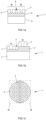
- the present description relates to a growth substrate 1 for the formation of optoelectronic devices.
- THE figures 1a and 1b schematically represent a section of two growth substrates. There figure 1c shows a top view of these substrates.
- Growth substrate 1 is intended to be placed in deposition equipment, such as an epitaxy frame, in order to form active layers of optoelectronic components on the exposed surface of substrate 1.
- This substrate 1 can also serve as a mechanical support allowing manipulation of the devices during the complementary manufacturing steps (formation of the electrical contacts, isolation of the devices from each other, etc.) leading to having a functional device.
- the growth substrate 1 comprises a growth support 2.
- This may be a circular wafer of materials, for example silicon or sapphire, of standardized size, for example 2 inches (50 mm), 4 inches ( 100 mm) or even 200 mm in diameter. But the growth substrate 1 is in no way limited to these dimensions or to this shape.
- the nature of the growth medium 2 is chosen to be able to withstand the treatments (such as deposits, heat treatments, etc.) implemented during the manufacture of the growth substrate 1 itself. and during production optoelectronic devices.
- the growth support 2 has a coefficient of thermal expansion similar or close to that of the materials which will form the useful layer of the optoelectronic device, in order to limit the significant stresses which could damage these devices at the end of their manufacture.
- the growth substrate 1 also comprises, arranged on the growth support 2, a plurality of crystalline semiconductor islands 3 (and designated more simply by the term “island(s)” in the remainder of this description).
- Each island 3 is intended to receive the active layers of an optoelectronic device, such as an LED, a laser or a photovoltaic cell.
- the islands 3 can be made of III-N materials.
- the islands 3 can consist of GaN or InGaN of wurtzite structure, whose axis c is perpendicular to the surface, and in which the proportion of indium can vary between 0% and 20%, and in particular between 1.5% and 8%.
- island is meant a block of material entirely separate from the other islands arranged on the growth support 2.
- crystalline is meant that the atoms constituting an island 3 are assembled in an orderly manner to form a block of monocrystalline material, this block may nevertheless include arrangement faults of the dislocation, slip plane or point fault type.
- the islands 3 are separated from each other via trenches 4. These trenches may have a lateral dimension, separating two islands 3, of between 0.1 and 50 microns, or 1 and 50 microns and typically of the order 2 microns or 20 microns. Each island has a relatively small size vis-à-vis the growth substrate, which can extend, in its largest dimension, for example between 1 micron to 1 mm, depending on the intended final application.
- the surface of the islands 3 can be between 1 ⁇ m 2 or 4 ⁇ m 2 and 1 mm 2 , and preferably between 25 ⁇ m 2 and 400 ⁇ m 2 .
- Each island 3 can have any shape, seen from above, for example circular, square, triangular, hexagonal or rectangular. Its thickness is typically less than 200 nm, in particular when it consists of InGaN.
- the islands 3 can all be of identical or different shapes and dimensions.
- the islands 3 do not all have the same mesh parameter.
- a first group of islands 3a has a first mesh parameter
- a second group of islands 3b has a second mesh parameter, different from the first.
- all the islands 3 are made of the same material.
- the materials of the islands 3 being identical to one another, the existence of a difference in lattice parameters denotes the existence of a different state of stress between the islands 3 constituting the two groups 3a, 3b.
- the materials of the islands 3 are not identical to each other from one group to another. Furthermore, the stress state of the islands 3 constituting the two groups 3a, 3b can also be different from one group to another. Consequently, the two groups of islands 3a, 3b have different lattice parameters.
- the variety of lattice parameters of the islands 3 of the growth substrate 1 will be used to collectively manufacture optoelectronic devices having distinct light properties, using a single manufacturing technology and on a single growth substrate.
- the first group of islands 3a which has the first lattice parameter
- a first LED emitting directly at a first wavelength for example in the green
- a second LED emitting directly at a second wavelength for example in the blue.
- directly emitting means that this emission corresponds to the light radiation emitted by the active layers (the quantum wells) of an LED, without requiring the use of conversion phosphorus.
- the growth substrate 1 can comprise at least a third group of islands, this third group having a third lattice parameter different from the first and from the second.
- the growth substrate can include any number of groups of islets, each group being formed of islets having a lattice parameter different from the islets belonging to the other groups. It will thus be possible to have a growth substrate 1 making it possible to form LEDs emitting in the field of red, green, blue and infrared wavelengths on the same substrate using a single technology.
- the distribution and arrangement of the groups of islands 3a, 3b on the surface of the growth medium 2 is not a essential characteristic, and all possible distributions and arrangements are possible. They can sometimes be dictated by the intended application.
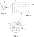
- first group of islands 3a occupies a first zone of the support 2 and the second group of islands 3b a second zone of the support 2, which are separate from each other and adjacent to each other.
- This arrangement is represented schematically in the figure 2a .
- Such a combination of LEDs constitutes a light pixel P whose emission color can be controlled.
- the islands 3, 3', 3" which will receive the constituent LEDs of these pixels P can be arranged in a regular manner on the surface of the growth support 2. It is thus possible to form monolithic pixels P, that is to say arranged on the same substrate and manipulated as a pixel, for example by a component insertion device, to be integrated into a functional device.
- the pixels P could for example be regularly distributed along rows and columns to form a matrix M, as shown in the figure 2b .
- a growth substrate 1 can comprise a plurality of such matrices M, as shown in the figure 2c .
- the growth substrate 1 also comprises at least one assembly layer 5 placed between the growth support 2 and the islands 3.
- the layer of assembly is directly in contact with the growth medium and with the islets 3, but the growth substrate could include other intermediate layers.
- This assembly layer 5 can comprise a dielectric such as a layer of silicon oxide or silicon nitride, or composed of a stack of such layers designed to, for example, facilitate subsequent removal of the growth support.
- the assembly layer 5 does not have a uniform thickness.
- the assembly layer has a first thickness in line with the islands 3 of the first group of islands 3a, and a second thickness, different of the first, to the right of the islets 3 of the second group of islets 3b. More generally, the assembly layer 5 has a distinct thickness in line with the islands of each of the groups of islands of the substrate 1.
- a strained crystalline semiconductor layer is first formed on a donor substrate. Then, this layer is transferred onto a substrate comprising a creep layer by bonding and by thinning and/or fracturing the donor substrate. Islands are then defined in the transferred layer, then the substrate and the islands are heat treated at a temperature above the viscous transition temperature of the creep layer, for example in BPSG, which leads to at least partial relaxation of the islets.
- the degree of relaxation obtained at the end of the thermal relaxation treatment can reach 70 to 80% or 95% of the maximum degree of relaxation corresponding to obtaining a perfectly relaxed layer. This degree of relaxation is dependent on the thickness of the islets, the duration and the amplitude of the heat treatment.
- the stiffener layer may be formed (or comprise) of a residue of the donor substrate which would have been preserved on the strained layer after its transfer to the creep layer. It may have been placed on the exposed face of the donor substrate to end up under the island at the end of the transfer of the strained layer and the formation of the islands.
- a relaxation substrate comprising a support 7, a creep layer 8 placed on the support 7 and, placed on the creep layer, a plurality of crystalline semiconductor islands 9 having a parameter of initial cell, at least part of this plurality of islands being constrained islands.
- a first group of islets 9a has a first lateral expansion potential and a second group of islets 9b has a second lateral expansion potential, different from the first.
- lateral expansion potential is meant the lateral expansion or contraction that an island 9 must undergo to reduce its elastic stress energy and balance it with the restraint energy of the creep layer 8 with which he is in touch.
- the methods also provide for thermal treatment of the relaxation substrate 6 at a relaxation temperature greater than or equal to the glass transition temperature of the creep layer 8 to cause the differentiated relaxation of the islands of the first and of the second group, the lattice parameter relaxed islands of the first group 3a and relaxed islets of the second group 3b then exhibiting different values
- a first manufacturing method comprises providing a relaxation substrate comprising a relaxation support 7, a creep layer 8 disposed on the support 7 and disposed on the creep layer 8, a plurality of semiconductor crystal islands constrained islands 9.
- the constrained islands 9 all have the same mesh parameter. Reference may be made to the cited documents of the state of the art to choose the nature of the relaxation support 7 and of the creep layer 8.
- the donor substrate may consist of a sapphire base support, a buffer layer of GaN formed on the base substrate and a strained layer of InGaN with an indium proportion between 1% or 1, 5% and 10% or 20% on the GaN buffer layer.
- Conventional steps of photolithography, resin deposition and etching may have been used to define, from the continuous layer of InGaN, the strained islands 9 of InGaN. These steps may have been applied before or after the transfer steps.
- the islands 3 can support a stiffening layer 10', residue of the donor substrate. It can thus act with a thickness comprised between 10 and 100 nm of GaN which initially formed the buffer layer of the donor substrate.
- the strained islands 9 of the relaxation substrate are selectively treated in a following stage of the manufacturing process so as to form a first group of strained islands 9a having a first potential for lateral expansion and a second group of constrained islands 9b presenting a second potential for lateral expansion, different from the first.
- the stress energy contained in an island of the first group 9a is different from the stress energy contained in an island of the second group 9b.
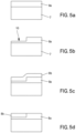
- Such a selective treatment may comprise the formation of a stiffening layer 10 having a first thickness on a first group of constrained islands 9a of the relaxation substrate 6 and a second thickness, different from the first, on a second group of islands 9b . This arrangement is shown on the figure 3c .
- This configuration of thickness of the stiffening layer 10 can be obtained by forming an initial stiffening layer of uniform thickness 10 'on all the islands 9, as shown in the figure 3b , then by selectively thinning this layer 10' to reduce its thickness on one of the two groups of islands 9a, 9b. It is again possible to use photolithographic masking steps to protect the stiffening layer 10 placed on one of the groups of islands from this thinning treatment. Alternatively to a thinning, it is also possible to choose to thicken the initial stiffening layer 10' on one of the two groups of islands 9a, 9b to achieve the configuration of the figure 3c . As we have seen, this stiffening layer 10' of uniform thickness can consist of a residue of the donor substrate.
- stiffening layer 10 can have a uniform thickness from one group of constrained islands 9a, 9b to the other.
- the stiffening layer 10 is typically made of a silicon oxide or a silicon nitride. But it can be any other material that is sufficiently rigid to modify the potential for lateral expansion of the island 9 on which it rests and, potentially, to avoid the warping of this island 9 during the thermal relaxation treatment that will follow. Depending on the nature of this layer, and the expected degree of relaxation of the island 9 on which it is placed, the stiffening layer 10 may have a thickness of between 10 nm and several hundred nm, such as 200 nm.
- the selective treatment aimed at differentially affecting the lateral expansion capacity of the islets 9 can also comprise the thinning of some of the islets 9, that is to say to reduce the thickness of the islets 9a of the first group of islets and/or the thickness of the islets 9b of the second group of islands so that these islands 9a, 9b, at the end of this treatment have different thicknesses. It may for example involve thinning at least one group of islets 9a, 9b from 10% to 50% of its initial thickness, in order to create a difference in thickness between these groups of islets which may be greater than 10 %.
- This variant is particularly useful when the stiffening layer has been formed between the flow layer 8 and the crystalline semiconductor island 9a, 9b, for example by placing a layer of stiffening material on the donor substrate, before the transfer of the layer stress on the relaxation support.
- the stiffening layer is formed under only some of the constrained islands 9.
- the stiffening layer can be formed beforehand, formed on the exposed surface of the donor substrate 11 and locally etched so as to selectively form islands with or without this layer. underlying, or with a variable thickness of this stiffener layer.
- the islands 9 having an underlying stiffening layer will have a lower lateral expansion potential than the islands without a stiffening layer, for an identical creep layer.
- the relaxation substrate 6 is heat treated at a temperature greater than or equal to the glass transition temperature of the creep layer 8.
- this heat treatment may comprise the exposure of the relaxation substrate to a temperature between 400°C and 900°C for a period of a few minutes to several hours. This is particularly the case when the creep layer is made of BPSG.
- the relaxation of the constrained islets 9 of the first and of the second group of islets 9a, 9b is caused to form at least partially relaxed islets 3, represented on the figure 3e .
- the degree of relaxation obtained during and at the end of the thermal relaxation treatment depends on the thickness of the island 9, the thickness and/or the nature of the stiffening layer 10 possibly covering this island 9.
- the constrained islets of the first group 9a and the constrained islets of the second group 9b having different characteristics and therefore a different lateral expansion potential, the heat treatment results in the initially constrained islets 9 of the first and second groups being relaxed to different degrees. 9a, 9b.
- the lattice parameter of the islets 3 of the first group 3a is different from the lattice parameter of the islets 3 of the second group 3b.
- a relaxation substrate 6 comprising a relaxation support 7, a creep layer 8 placed on the support 7 and, placed on the creep layer 8, a plurality of strained semiconductor crystalline islands 9.
- the strained islands 9 all initially have the same mesh parameter.
- the creep layer 8 is composed of a first group of blocks 8a and a second group of blocks 8b.
- each group 8a, 8b is made up of a single block for reasons of simplification of the description, but in general, a group of blocks can be made up of one or a plurality of blocks.
- the term “block” should be understood in a very broad sense, designating any block or combination of blocks of homogeneous material, this block defining any volume, which is not necessarily convex.
- the blocks of the first group 8a and the blocks of the second group 8b consist of different materials, which for a determined temperature, respectively have a first and a second viscosity which are different from each other.
- the constrained islands 9 arranged on the blocks 8a of the first group form a first group of constrained islands 9a and, similarly, the constrained islands 9 arranged on the blocks 8b of the second group form a second group of constrained islands 9b.
- the constrained islands 9 are likely to relax, at least partially, in a differentiated manner.
- the constrained islets of the first group 9a have a different relaxation potential from the relaxation potential of the constrained islets 9b of the second group.
- the strained islands 9 are all of the same size, the stress energy that they contain are also quite similar, but the nature of the blocks on which they rest being different, the islands 9 are likely to relax in a differentiated manner .
- the strained islands 9 may come from a donor substrate 11, and have been transferred to the flow layer 8 of the relaxation substrate 6 by steps identical or similar to those presented in relation to the description of the first method.
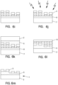
- THE figures 5a to 5d represent a sequence of possible steps to produce a creep layer 8 composed of blocks 8a, 8b of different viscosities.
- a first creep layer 8a is formed on the support 7. It may be a dielectric layer of silicon dioxide, or silicon nitride, comprising a determined proportion of boron and/or phosphorus to give it a first viscosity value.
- at least one recess 10 is provided by partial masking and etching of the first creep layer 8a.
- the recess 10 can be partial, as shown in the figure, or correspond to the entire thickness of the first creep layer 8a.
- the remaining first layer 8a and the recess 10 are covered with a second creep layer 8b.
- This second layer 8b preferably, has a sufficient thickness to completely fill the recess 10.
- the material constituting the second creep layer 8b is of a different nature from the first layer 8a so that the first and the second layer have a different viscosity. when exposed to a specified relaxation temperature.
- This different viscosity can be either higher or lower than that of the first layer 8a.
- the first layer is made of silicon dioxide or silicon nitride, which has particularly high viscosities, it will be possible to choose the material of the second layer 8b in BPSG, with a sufficient proportion by mass of boron and phosphorus, by example greater than 4%, to have a lower viscosity than that of the first layer.
- the exposed surface of the substrate is then planarized to eliminate the second creep layer outside the recesses 10 until the first creep layer 8a is exposed. In this way, the first blocks 8a and the second blocks 8b constituting the creep layer 8 are formed. .
- the relaxation substrate 6 is heat treated at a relaxation temperature greater than or equal to the glass transition temperature of the creep layer, that is to say of at least one of the first and second blocks 8a, 8b of the creep layer 8 to cause the differentiated relaxation of the islands 9a, 9b of the first and the second group.
- the heat treatment may comprise the exposure of the relaxation substrate 6 to a relaxation temperature of between 400° C. and 900° C. for a period of a few minutes to several hours. This causes the lateral expansion of the constrained islands 9 of the first and the second group of islets 9a, 9b to form at least partially relaxed islets 3, represented on the figure 4c .
- the constrained islets of the first group 9a and the constrained islets of the second group 9b resting on blocks having a different viscosity at the relaxation heat treatment temperature, and therefore having a different lateral expansion potential
- the heat treatment results in the initially constrained islands 9 of the first and second groups 9a, 9b being relaxed to different degrees, and in causing their differentiated lateral expansion. Consequently, at the end of the thermal relaxation treatment, the lattice parameter of the islets 3 of the first group 3a is different from the lattice parameter of the islets 3 of the second group 3b.
- This third method comprises the preparation of a donor substrate 11 comprising a plurality of strained elementary layers of crystalline semiconductors 12a, 12b forming a stack 12.
- the stack has at least a first zone 13a and a second zone 13b having levels different constraints.
- the first step of preparing the donor substrate 11 has been shown. It comprises supplying a base substrate 14, for example consisting of sapphire, silicon or silicon carbide.
- a stack 12 of elementary semiconductor and crystalline layers is formed on the base substrate 14, each layer of the stack having a different nature.
- two elementary crystalline semiconductor layers 12a, 12b have been formed.
- the first elementary layer 12a may be a layer of gallium nitride having a thickness of 2 microns or more, forming a buffer layer and whose upper part is essentially relaxed.
- the second elementary layer 12b may be a layer of InGaN with a thickness of around 100 nm and the proportion of indium of which is around 6%.
- the second elementary layer 12b of the stack 12, and in general each elementary layer of the stack 12, has a thickness less than its critical relaxation thickness. At least some of the layers are therefore stressed, in compression in the example taken above. In this way, the second elementary layer 12b (or each layer of the stack 12 formed on the first elementary layer 12a) is pseudomorphic and therefore has a lattice parameter identical to that of the first layer 12a of the stack 12.
- FIG. 6b a following step in the preparation of the donor substrate 11, consisting in locally eliminating the second elementary layer 12b to expose part of the first elementary layer 12a.
- This elimination step can implement traditional means of photolithographic masking and etching, for example dry etching.
- a first zone 13a in which the first layer 12a is exposed, and a second zone 13b where the second layer 12b of the stack is exposed, are defined in this way, on the exposed surface of the donor substrate 11.
- part of the stack 12 is locally eliminated so as to preserve, in respective zones 13, only part of the layers forming the stack 12.
- the zones 13 have different stress levels. one from the others, since each zone 13 is respectively formed from a different stack of one or a plurality of elementary layers, each in a different state of stress.
- zone 13a consists of first layer 12a and has a first reference stress level.
- Zone 13b consists of the stack formed of the first elementary layer 12a and the second elementary layer 12b strained. The second zone 13b therefore has a stress level higher than that of the first zone 13a.
- Zones 13a, 13b are not necessarily all in one piece, that is to say the local elimination of the elementary layers of the stack 12 to expose a particular layer can be carried out at a plurality of locations. distinct and not joined.
- the term "zone” will denote the collection of locations on the surface of the donor substrate 11 exhibiting the same stress level, for example for which the same layer 12a, 12b of the stack 12 is exposed at the end of this elimination step.
- the first and the second zone 13a, 13b of the donor substrate will each make it possible respectively to form the islets 3 of the first and of the second group of relaxed islets 3a, 3b of a growth substrate 1. It will therefore be sought to define these zones at the surface of the donor substrate 11 so that they correspond to the chosen arrangement of the islets 3 of the groups of islets 3a, 3b, as has been explained previously in relation to the figures 2a to 2c .
- the following stages of preparation of the donor substrate 11, represented on the figures 6c and 6d aim to prepare the transfer of the stack 12 thus defined on a relaxation support 7.
- an adhesive layer 15 having a flat and smooth exposed surface. It may be a layer of dielectric, for example silicon dioxide or silicon nitride. When it comes to silicon dioxide, the latter may include boron and/or phosphorus to give it creep properties when the bonding layer 15 is exposed to a temperature above its glass transition temperature.
- This bonding layer 15 is deposited with a sufficient thickness to make it possible to completely encapsulate the stack 12 and thus provide a flat surface. When its formation provides for the application of a polishing step, the removal of thickness which occurs during this treatment will be taken into account. By way of example, a thickness of 500 nm or more of the material can be deposited to form the bonding layer 15.
- light species such as hydrogen or helium
- the introduction of these species results in the formation of a fragile plane 16 making it possible to eliminate, in a later stage of the manufacturing process, the base substrate 14 and allowing the transfer of the stack 12 to the relaxation support 7.
- the plane fragile 16 can preferably be located in the base support 14 or in the first elementary layer 12a of the stack 12, so that the stack 12 is actually transferred onto the support 7.
- this third manufacturing method is in no way limited to a transfer implementing the formation of a weakening plane 16. It is possible to envisage carrying out the transfer on the support 7 by mechanical-chemical removal of the base support 14 especially when it is made of silicon. We can also consider its detachment by laser irradiation of the interface separating the base substrate 14 and the first elementary layer 12a, in particular when this base substrate is made of sapphire.
- the relaxation support 7 has been provided beforehand with a creep layer 8 so that after the operation of removing the base support 14, there is a relaxation substrate 6 comprising the relaxation support 7, the layer creep 8, bonding layer 15, and stack 12 of elementary layers of strained crystalline semiconductors defining areas 13 having different stress levels.
- trenches 4 are made in the stack 12 so as to define constrained islands 9.
- the trenches 14 are made in the stack 12 to define the islands 9 of a first group 9a in the first zone 13a, and the islands 9 of a second group of islands 9b in the second zone 13b.
- These trenches 4 can penetrate into the bonding layer 15 or even into the flow layer 8.
- This step of defining the islands 9 can be carried out after the transfer of at least part of the stack 12 as has been presented here , but it is also possible to envisage carrying out this step prior to the transfer of the stack 12, directly on the donor substrate 11. As we have seen, the formation of the trenches 4 can lead to defining islands 9 of shapes and dimensions very varied.
- a relaxation substrate 6 comprising a support 7, a creep layer 8 placed on the support and an adhesive layer 15 placed on the creep layer 8 is available.
- the creep layer 8 and the bonding layer 15 can both be made of BPSG and therefore have creep properties.
- the relaxation substrate 6 also comprises, on the creep layer 8, a plurality of crystalline semiconductor islands all having the same initial lattice parameter.
- a first group of islands 9a has a first level of constraints. These are the islands 9 which have been formed in the stack 12 at the level of the first zone 13a of this stack.
- a second group of islands 9b has a second level of constraint, different from the first. These islands 9 of the second group 9b are those which have been formed in the stack 12 at the level of the second zone 13b of this stack.
- the relaxation substrate 6 can comprise a plurality of groups of islands having between them different stress levels, each group of islands having been formed, in the stack 12, at the level of a zone 13 distinct from this stack 12.
- the constrained islands 9 of each group of islands have a different lateral expansion potential from one group to another.
- the stress energy contained in an island 9 of the first group 9a is different from the stress energy contained in an island 9 of the second group 9b.
- the relaxation substrate 6 may for example be a heat treatment bringing the substrate 6 to 800° C. for four hours. More generally, the relaxation temperature of this heat treatment will be chosen so that it exceeds the glass transition temperature of the creep layer 8, and possibly that of the bonding layer 15 when the latter has properties of creep. This relaxation temperature is typically between 400°C and 900°C. The heat treatment can last between 30 minutes and several hours.
- the islets forming the different groups of islets 9a, 9b initially exhibiting different stress levels the application of the thermal relaxation treatment leads to the relaxation and to the differentiated lateral expansion of the islets of a group to another.
- the relaxed islets 3 of the first group 3a and the islets 3 of the second group 3b then have different lattice parameters.
- the islets 3 can for example be transferred to a growth support 2 via an assembly layer 5.
- the islets 3 are covered with the assembly layer 5, this layer is assembled, which may have undergone treatments to facilitate this, to Growth Support 2 ( figure 6k ) and eliminates the relaxation support 7 by any appropriate means to obtain the structure of FIG. 3l.
- the flow layer 8 and the bonding layer 15 are then removed from the structure obtained. Additional etching steps can make it possible to remove the excess assembly layer 5, thus making it possible to have a growth substrate 1 ( figure 6m ) as previously described in relation to the figure 1b .
- the degree of relaxation obtained during and at the end of the thermal relaxation treatment depends, among other things, on the size of an island 9, its level of stress, and the nature of the creep layer 8 on which it rests, and more particularly the viscosity of the material which makes up this layer (or this block in the case of the second method).
- This transfer may include transferring the islets to an intermediate support, before transferring them to this other support.
- This provides a growth substrate that does not include a creep layer, which may be incompatible with the steps for manufacturing the active layers of optoelectronic devices.
- this transfer makes it possible, in the case where the islands consist of a polar material, to recover on the exposed face of the growth medium 1 the initial polarity of this material, as it had been formed on the donor substrate.
- a method for the collective manufacture of a plurality of optoelectronic devices is described.
- the invention relates to this method of using the growth substrate.
- These devices each comprise active layers which may be different from one device to another.
- the devices then have different optoelectronic properties from each other.
- collective fabrication it is meant that the fabrication of these devices employs a single technology applied to a single substrate to form the active layers.
- This method comprises the supply of a growth substrate 1, in accordance with the general description which has just been given. It therefore comprises at least a first group of crystalline semiconductor islands 3a having a first lattice parameter and a second group of crystalline semiconductor islands 3b having a second lattice parameter, different from the first.
- the next step aims to form the active layers by growth on the exposed face of these islands 3.
- the growth substrate is placed for this in a deposition chamber, for example that of a frame of epitaxy.
- a deposition chamber for example that of a frame of epitaxy.
- gases comprising the atomic elements constituting the active layers which it is desired to deposit on the islands 3.
- the precursor gases are brought to temperature above the substrate of growth 1 so as to release the atomic elements, and allow their adsorption on the surface of the growth substrate 1 and in particular on the surface of the islands 3.
- the relative concentration and the duration of circulation of these precursor gases it is possible control the nature and the thickness of the layers which are gradually formed on the crystalline semiconductor islands 3.
- dopants of p or n type
- the precursor gases may form, on the islands, active layers of electronic devices, such as quantum wells or heterostructures of LEDs.
- the precursor gases to form these active layers of LEDs can include trimethylegalium (TMGa), triethylgallium (TEGa), trimethylindium (TMIn) and ammonia (NH3).
- the incorporation of certain atomic elements of the precursor gases into the deposited layer is affected by the lattice parameter of this layer. This is particularly the case with regard to the incorporation of indium in an InGaN layer as reported in the document " Strain effects on indium incorporation and optical transitions in green-light InGaN heterostructures of different orientations. by MV Durnev et al, Phys. Status Solidi A 208, No. 11, 2671-2675 (2011 ). It appears that the solubility of indium in a material increases when the lattice parameter of this material increases. In other words, and all other things being equal, the incorporation of indium into a material during its formation by deposition increases with the lattice parameter of the material in which it is incorporated.
- the method implements a step of exposing the growth substrate 1 to an atmosphere comprising at least an initial concentration of an atomic element.
- the atomic element On the islands 3 of the first group 3a of the growth substrate 1, which has a first lattice parameter, the atomic element is incorporated into the active layer in a first concentration. On the islands 3 of the second group of islands 3b, which has a second lattice parameter different from the first, the atomic element is incorporated into the active layer according to a second concentration, different from the first. If the second lattice parameter is greater than the first, the second concentration will be greater than the first.
- the first and the second concentration are determined by the initial concentration of the atomic species in the chamber and by the first and the second lattice parameter of the islands.
- other parameters can also influence the nature of the layers that form, such as the pressure of the chamber, the temperature, the respective flow rate of the precursors, etc.
- the proportion of indium incorporated into the active layers of InGaN deposited on the islands of the first group of islands can lead to the formation of LEDs directly emitting radiation in the blue range.
- the proportion of indium incorporated into the active layers of InGaN deposited on the islands of the second group of islands can lead to the formation of LEDs directly emitting radiation in the green range.
- the process for manufacturing the electronic devices can be continued, in particular to form the electrical contacts and isolate the devices from each other, as described for example in the document US9478707 . It is also possible to transfer islands 3 provided with their active layers onto a support of LEDs, and to eliminate the growth support 2.
- a particular application of the growth substrate and of the collective manufacturing process which have just been described aims to manufacture a monolithic micro panel of LEDs.
- a micro panel consists of an arrangement of LEDs, generally all identical and of very small size, arranged at constant pitch in rows and columns on a panel support.
- the micro panel is said to be “monolithic”. This characteristic is advantageous, because the LEDs then have very similar properties (such as current and/or voltage behavior, evolution with aging, etc.), which facilitates the design and manufacture of the micro panel.
- a monolithic LED micro-panel will denote a micro-panel in which all the LEDs have been collectively manufactured and collectively extracted from the same manufacturing support to form the micro-panel; or a micro panel composed of monolithic pixels, i.e. each pixel is made up of collectively manufactured LEDs extracted from the same manufacturing support. In this case, the monolithic pixels are assembled together to form the micro panel.
- the monolithic micro-panel of LEDs can be assembled with a control circuit by direct chip transfer technology (often referred to by the Anglo-Saxon name "Flip Chip”) making it possible to electrically connect each LED of the micro-panel with a drive circuit of the driver circuit.
- This assembly may consist in assembling an entire monolithic micro panel to a driver circuit, each LED of the micro panel being after assembly associated with a driver circuit. Or the assembly may consist of successively assembling one or a plurality of monolithic pixels to the driver circuit to associate them with the driver circuit. Whichever approach is chosen, a monolithic display microscreen is thus formed.
- the drive circuits of the driver circuit can also have the same or similar electrical properties, which greatly facilitates the manufacture of the display microscreen.
- the known monolithic micropanels are all made up of LEDs directly emitting a single wavelength, thus allowing a monochrome display.
- the color display is obtained by means of conversion phosphor placed on the emission face of some of these LEDs, or by optically combining a plurality of micro panels each emitting radiation chosen in a combination of complementary colors, for example red, green and blue.
- the methods and substrates in accordance with the present description make it possible, on the contrary, to propose a monolithic micro panel of LEDs comprising a panel support and a plurality of LEDs arranged on this panel.
- the plurality of LEDs comprises a first group of LEDs capable of directly emitting light radiation exhibiting a first wavelength, and a second group of LEDs capable of directly emitting a second light radiation exhibiting a second wavelength different from the first one.
- a micro panel is therefore capable of emitting different colors without requiring optically combining a plurality of micro panels or applying conversion means.
- the micro panel comprises at least three groups of LEDs, each group emitting at a different wavelength from the others. It is for example possible to have a first group of LEDs emitting directly in the red, a second group of LEDs emitting radiation directly in the green and a third group of LEDs emitting radiation directly in the blue. It is also possible to envisage having a fourth group of LEDs emitting directly in the infrared, this illumination being able to be used to provide additional functionalities to the device integrating the micro panel (touch function, recognition of the iris of the eye, motion detection, etc.).
- the LEDs of each group are arranged regularly on the panel support, for example spaced apart at a constant pitch along rows and columns, in order to form a display matrix. They are also arranged to place side by side, or more precisely close to each other, an LED of each group, so as to form at each location of the matrix a light pixel whose color can be controlled.
- the size of the LEDs can vary according to the group in order to play on the distribution of the luminous intensities of the different colors of emission. For example, the red LEDs may be larger than the blue and green LEDs.
- the micro panel can be made up of LEDs making it possible to form a matrix of pixels of large dimensions, for example 50 pixels by 50 pixels, or 200 pixels by 200 pixels, or even more.
- the luminous pixels of the panel consist of LEDs emitting in different wavelengths
- these LEDs have been collectively formed from a single technology and on a single substrate. They therefore have properties, and in particular electrical and aging properties, which are very similar to each other, which makes it possible to associate them with a control circuit consisting of driver circuits which are all identical or very similar.
- a growth substrate 1 comprising on a growth support 2 provided with an assembly layer of silicon oxide 3 is first prepared.
- the growth support may for example consist of a wafer of 150 mm diameter sapphire.
- the growth substrate comprises three groups of islands 3a, 3b, 3c of InGaN comprising 8% indium.
- the islands 3a, 3b, 3c all have a thickness of 200 nm and a square shape with sides of 50 microns.
- the first group of islands 3a has a lattice parameter of 0.3190 nm
- the second group has a lattice parameter of 0.3200 nm
- the third group has a lattice parameter of 0.3205 nm.
- the islets 3 constituting each of these groups are distributed and arranged on the growth support 2 according to a matrix arrangement in accordance with what has been explained in relation to the description of the figures 2a to 2c .
- Three islands 3, 3', and 3" of each of the groups are therefore arranged close to each other so as to define a pixel; and these groupings of islands distributed in a matrix along rows and columns on the surface of the substrate growth 1. It is possible to provide panel trenches 4′ wider than the trenches 4 separating two islands to separate the matrices from each other, each matrix delimiting a set of islands 3, 3′, 3′′ intended to receive the LEDs of a micro panel.
- a relaxation substrate 6 is first prepared comprising a relaxation support 7, for example in sapphire also 150 mm, and a flow layer composed of BPSG.
- the relaxation substrate also comprises strained islands 9 of InGaN comprising 8% indium. These constrained islands 9 are arranged similarly to what has just been described for the relaxed islands 3 of the growth substrate 1.
- the parameter of the same for the constrained islands 9 is 0.3185 nanometer.
- the strained islands 9 are covered with an initial stiffening layer 10' of GaN 50 nm thick, the residue of a buffer layer of GaN from a donor substrate having been used to produce the relaxation substrate.
- a thermal relaxation treatment is carried out, for example at 800° C. for one hour. This treatment leads to the relaxation of the initially constrained islets 9, to form partially relaxed islets 3 which, at the end of the thermal relaxation treatment, have a lattice parameter close to 0.3190 nanometer. If this is not the case, the application of the thermal relaxation treatment can be repeated, possibly by thinning the initial stiffening layer to promote the relaxation of the islets 3.
- the stiffener layer 10' which covers the islands 3 of the second and third groups is then eliminated by etching, and the relaxation heat treatment is repeated. Provision can also be made to thin the islands 3 of the second and third group, for example by 40 nm, to promote their relaxation.
- the lattice parameter of the islands of the first group, covered by the layer of stiffener 10 has varied relatively little, close to 0.3190 nm.
- the lattice parameter of the islands of the second and the third group has grown to be close to 0.3200 nm.
- the islets of the third group are thinned, for example by 70 nm, and the thermal relaxation treatment is again applied.
- the lattice parameters of the islands of the first and second group remain relatively constant, and are in any case less affected by this heat treatment than the lattice parameter of the islands of the third group which is then close to 0.3205 nm.
- This final relaxation heat treatment can be repeated, possibly in combination with a thinning of the stiffener layer placed on the islands of the first group or a thinning of the islands of the second and second group, to make the mesh parameters of these islands converge towards their target mesh parameters.
- the repetition of these steps leads to the selective relaxation of the groups of islets and, at the end of these steps, the first group of islets 3a has a lattice parameter of, or close to 0, 3190 nanometer, the second group has a lattice parameter of or close to 3.200 nanometers and the third group has a lattice parameter of or close to 3.205 nm.
- the partially relaxed islands 3 of InGaN are then transferred by bonding to a growth support 2 provided with an assembly layer 5, for example a multilayer of silicon dioxide and nitride.
- TMGa precursor gas
- TEGa precursor gas
- TMIn precursor gases
- the lattice parameters of the islands of the first group, the second group and the third group of islands are different from each other, the incorporation of indium into the active layers of InGaN which form on the islands of these groups is also different.
- LEDs are obtained which directly emit radiation in the blue domain, on the islands of the second group LEDs which directly emit radiation in the green domain, and on the islands of the third group LEDs are formed. directly emitting radiation in the red range.
- an active layer of LEDs arranged at the level of a pixel and emitting colors in the red, green and blue range.
- the wafer on which the LEDs which have just been formed rest can be cut according to the trenches 4' defining the pixel matrices. Each of these matrices then constituting a micro panel.
- the wafer comprising the micro-panels to a second wafer on which pilot circuits consisting of a matrix of drive circuits have been formed.
- Each matrix is arranged on the surface of this wafer according to the same arrangement as the LEDs on the growth substrate.
- the assembly makes it possible to put each diode in electrical contact with a driver circuit.
- a plurality of display screens are formed in a single contacting step. It is then possible to choose to eliminate the growth medium 2, for example by laser irradiation, and the assembly layer 5, for example by chemical etching, so as to expose a light-emitting surface of the LEDs. These surfaces can be prepared with optical elements, coatings or surface protection to improve the quality and robustness of the screen.
- the wafer can be cut in a conventional manner so as to isolate the screens from each other for the purpose of packaging them.
- the second and third layer it is possible to provide an intermediate layer of AlGaN comprising between 0% and 10% aluminum and with a thickness of between 1 and 3 nm.
- This intermediate layer makes it possible to ensure that the stack 12, in particular the third elementary layer, is indeed pseudomorphic, that is to say that all the elementary layers all have the same lattice parameter. As the concentration of indium from one layer to another increases, the stress level of each layer also increases.
- the first, second and third elementary layers are exposed at three zones of the donor substrate. Each zone is respectively distributed on the surface of the donor substrate 11 according to the pixel and matrix distribution presented in relation to the figures 2a to 2c .
- a bonding layer 15 500 nm thick is prepared, comprising silicon dioxide and boron and phosphorus in a mass proportion of 4%.
- the bonding layer is polished to allow its assembly to a sapphire growth support 7.
- the stack 12 of the elementary layers is then transferred to a sapphire relaxation support 7, also 150 mm in diameter, for example according to the invoice implantation technique detailed in the general description of the process.
- the sapphire substrate 7 has previously been provided with a creep layer 8 of BPSG, that is to say comprising silicon dioxide and boron and phosphorus, here in a mass proportion of 4% phosphorus and 6 % boron.
- the islands 9a of the primer group of islands are defined in the first zone 13a
- the islands 9b of the second group are defined in the second zone
- the islands of the third group are defined in a third zone of the stack.
- the islands 9a, 9b are here all square and have a side of 10 microns.
- the islands 9 of the first group consist of a single layer of GaN, the first elementary layer which is essentially relaxed.
- the islands 9 of the second group consist of a stack formed of a GaN layer and an InGaN layer comprising 6% indium, the second strained elementary layer.
- the islands of the third group consist of a stack formed of a GaN layer, an InGaN layer comprising 8% indium (the second elementary layer) and an InGaN layer comprising 16% indium. indium (the third elementary layer).
- a first thermal relaxation treatment is carried out aimed at causing the creep layer 8 and the bonding layer 15 to flow and to release the stresses of the islands.
- the step is carried out at 800° C. for 4 hours.
- the islands 9 of the first group of islands are not constrained, their lattice parameter therefore does not change during this heat treatment.
- the islands of the second and the third group are composed of a stack of layers having different stress levels.
- the lattice parameter of these islands tends towards the equilibrium lattice parameter of the stack of layers which constitutes them.
- the parameter obtained will be close to the lattice parameter of the (In,Ga)N alloy of average composition over the thickness of the stack.
- the islets are partially etched to thin them.
- the etched thickness is typically around 100 nm.
- the thickness of the islands is then approximately 50 to 60 nm.
- the creep of the creep layer 8 and of the bonding layer 15 is again caused by applying a new thermal relaxation treatment to release the residual stresses of the islands of the second and third group.
- the conditions of the second heat treatment are identical to the conditions of the first.
- the thermal relaxation treatment can be renewed, optionally in combination with a thinning of the islets, to make their lattice parameters converge towards their target lattice parameters.
- the repetition of these steps leads to the differentiated relaxation of the groups of islets and, at the end of these steps, the first group of islets 3a has a lattice parameter typically between 3.180 A and 3.190 A, the second group has a lattice parameter between 3.210 A and 3.225 A, and the third group has a lattice parameter between 3.240 A and 3.255 A.
- the relaxed or partially relaxed islets 3 are then transferred by bonding to a growth support 2 provided with an assembly layer 5, for example a multilayer of silicon dioxide and nitride.
- a growth substrate 1 is thus formed. This process can be continued similarly to that of example 1, by growing active layers of nitride-based LEDs on each of the islands and by completing the manufacture of functional LEDs on the growth substrate, in particular by forming the LED contacts on either side of the active layers, or in the form of a monolithic panel.
- a growth substrate 1 is prepared comprising, on a growth support 2 provided with an assembly layer 5 composed of a stack of 500 nm of carbon oxide. silicon in contact with the sapphire support, 200nm of silicon nitride, and one micron of silicon dioxide.
- This stack is designed to allow the detachment by laser irradiation of the growth medium in a subsequent step of the process.
- This growth medium may for example consist of a sapphire wafer 150 mm in diameter.
- the growth substrate has three groups of islands of InGaN comprising 18% indium. The islands all have a thickness of 40 nm and a square shape with sides of 10 microns.
- the first group of islands has a lattice parameter of 0.3184 nm
- the second group has a lattice parameter of 0.3218 nm
- the third group has a lattice parameter of 0.3248 nm.
- the islets 3 constituting each of these groups are distributed and arranged on the growth support 2 according to a matrix arrangement in accordance with what has been explained in relation to the description of the figures 2a to 2c and the two previous examples.
- a relaxation substrate 6 is first prepared comprising a relaxation support 7, for example in sapphire also of 150 mm, to form a flow layer 8 thereon.
- the preparation of the flow layer firstly comprises the formation of a disassembly layer composed of a stack of 500 nm of silicon oxide in contact with the sapphire support and of 200 nm of silicon nitride.
- This disassembly stack is designed to allow detachment by laser irradiation of the relaxation support 7 in a later stage of the process.
- a first layer of one micron of silicon dioxide is formed on the dismantling layer.
- recesses are formed in the first layer arranged on the surface of the support to be in correspondence with the islands of the second group and reducing the thickness of the first layer of silicon dioxide to 100 nm.
- a second layer about one micron thick, this second layer consisting of silicon dioxide and a mass proportion of 3% of boron and 4% Phosphorus.
- Masking steps by photolithography and etching are repeated to form new recesses, this time arranged on the surface of the substrate to be matched with the islands of the third group.
- the etching is carried out to remove the entire thickness of the second layer of BPSG and preserve a thickness of 100 nm of the first layer of silicon dioxide.
- a third layer consisting of silicon dioxide and a mass proportion of 4% boron and 4% phosphorus is then deposited.
- the surface is planarized to partly eliminate the third and second layers so as to form the first, second and third group of blocks constituting the creep layer 8.
- the relaxation substrate also comprises strained islands 9 of square InGaN with sides of 10 microns comprising 18% indium transferred onto the creep layer 8 according to a layer transfer method detailed in the general description, and by producing sliced 4. These constrained islands 9 are arranged similarly to what has just been described for the relaxed islands 3 of the growth substrate 1.
- the lattice parameter of the constrained islands 9 is 0.3184 nanometer. Each constrained island 9 rests on a tile of one of the first, second and third groups, thus defining a first, a second and a third constrained island group.
- the strained islands 9 are covered with an initial stiffening layer of GaN 50 nm thick, residue of a buffer layer of GaN from a donor substrate having been used to produce the relaxation substrate.
- a thermal relaxation treatment is carried out, for example at 750° C. for one hour. This treatment leads to the lateral expansion of the initially constrained islands 9, to form partially relaxed islands 3.
- the viscosity of the blocks of the third group is estimated at 1E10 Nm -2 .s -1 approximately, that of the blocks of the second group is estimated at approximately 4E10 Nm -2 .s -1 , and that of the blocks of the first group, made of silicon dioxide, is not viscous, that is to say it has a viscosity greater than 1E12 Nm -2 .s -1 .
- the stress relaxation rate in the islets of the third group is 90%, so they have a lattice parameter of 3.246 ⁇ .
- the stress relaxation rate in the islets of the second group is about 50%, giving a lattice parameter of 3.218 ⁇ .
- the lattice parameter of the islets of the first group has not changed and remains at 3.184 ⁇ .
- the estimated viscosity values are given by way of example only.
- the heat treatment time can be adjusted so that the relaxation rate of the island placed on the block of intermediate viscosity is at the end of the process between 40 and 60%, and the relaxation rate of an island laid out on a pavement of lower viscosity is higher than 70%.
- the lattice parameters of the islands of the first, second and third group are respectively 3.184 ⁇ , 3.218 ⁇ and 3.248 ⁇ approximately, ie to within 0.005 ⁇ .
- the partially relaxed islands 3 of InGaN are then transferred by bonding to a growth support 2 provided with an assembly layer 5, for example a multilayer of silicon dioxide and nitride.
- assembly layer 5 for example a multilayer of silicon dioxide and nitride.
Description
La présente invention concerne un procédé d'utilisation d'un substrat de croissance pour fabriquer collectivement une pluralité de dispositifs optoélectroniques comportant des couches actives de compositions différentes. L'invention trouve une application toute particulière dans le domaine des micro-écrans d'affichage.The present invention relates to a method of using a growth substrate to collectively manufacture a plurality of optoelectronic devices comprising active layers of different compositions. The invention finds a very particular application in the field of display micro-screens.
Les documents
Le document
De multiples produits combinent des DELs émettant à des longueurs d'onde différentes pour former un point lumineux coloré. C'est le cas notamment des écrans d'affichage permettant de former une image composée de pixels, chaque pixel associant une DEL rouge, verte et bleu, dont on peut contrôler individuellement l'émission afin de former, par combinaison des émissions lumineuses, un point lumineux de couleur choisie.Multiple products combine LEDs emitting at different wavelengths to form a colored light point. This is particularly the case of display screens making it possible to form an image made up of pixels, each pixel associating a red, green and blue LED, the emission of which can be individually controlled in order to form, by combining the light emissions, a light point of a chosen color.
Les DELs qui sont associées pour former le pixel ne sont généralement pas fabriquées à partir des mêmes matériaux et des mêmes technologies. Ainsi, les DELs bleues ou vertes peuvent être formées à partir de nitrure (de formule générale InGaN), et les DELs rouges à partir de phosphure (de formule générale AlGaInP) . La fabrication d'un écran met en oeuvre l'assemblage, une à une, des diodes pour former les pixels du dispositif final, par exemple par une technique d'insertion de composants (« Pick and Place » selon la terminologie anglo-saxonne) .The LEDs that are combined to form the pixel are generally not made from the same materials and the same technologies. Thus, blue or green LEDs can be formed from nitride (general formula InGaN), and red LEDs from phosphide (general formula AlGaInP). The manufacture of a screen involves the assembly, one by one, of the diodes to form the pixels of the final device, for example by a component insertion technique (“Pick and Place” according to the English terminology) .
Les matériaux n'ayant pas les mêmes propriétés, les caractéristiques de vieillissement, de comportement thermique, électrique et/ou d'efficacité des dispositifs qui les exploitent sont généralement bien différentes. Ces variabilités doivent être prises en compte lors de la conception d'un produit intégrant des DELs formées à base de matériaux différents, ce qui rend cette conception parfois complexe.Since the materials do not have the same properties, the characteristics of ageing, thermal and electrical behavior and/or the efficiency of the devices that use them are generally very different. These variabilities must be taken into account when designing a product integrating LEDs formed from different materials, which sometimes makes this design complex.
D'autres solutions prévoient de former les pixels à partir de diodes toutes identiques, fabriquées sur un même substrat et/ou à l'aide de la même technologie. On peut alors réaliser des micro panneaux monolithiques de DELs, présentant une dimension réduite, et une résolution importante. A titre d'exemple d'une telle réalisation, on pourra se référer au document «
On connaît également de l'état de la technique les documents :
- «
Emission color control from blue to red with nanocolumn diameter of InGaN/GaN nanocolumn arrays grown on same substrate », applied physics letters, vol 96, n°23 , 7 juin 2010 - "
Sélective Area Métal Organic Vapor Phase Epitaxy of Nitride Semiconductors for multicolor Emission", IEEE journal of selected topics in quantum electronics, vol 15, n°4, 1er juillet 2009
- "
Emission color control from blue to red with nanocolumn diameter of InGaN/GaN nanocolumn arrays grown on same substrate”, applied physics letters, vol 96, n°23 , 7 juin 2010 - "
Selective Area Metal Organic Vapor Phase Epitaxy of Nitride Semiconductors for multicolor Emission", IEEE journal of selected topics in quantum electronics, vol 15, n°4, July 1, 2009
Afin de parer aux limitations qui viennent d'être exposées, il serait souhaitable de pouvoir fabriquer simultanément sur un même substrat, à partir d'une même technologie, des DELs pouvant émettre dans des longueurs d'onde différentes. D'une manière plus générale, il serait avantageux de fabriquer collectivement des dispositifs ayant des propriétés optoélectroniques pouvant être différentes les unes des autres.In order to circumvent the limitations which have just been explained, it would be desirable to be able to manufacture simultaneously on the same substrate, using the same technology, LEDs capable of emitting in different wavelengths. More generally, it would be advantageous to collectively manufacture devices having optoelectronic properties which may be different from each other.
L'invention propose un procédé d'utilisation d'un substrat de croissance selon la revendication 1
- D'autres caractéristiques avantageuses et non limitatives de cette utilisation sont définies par les revendications dépendantes
- Other advantageous and non-limiting characteristics of this use are defined by the dependent claims
D'autres caractéristiques et avantages de l'invention ressortiront de la description détaillée de l'invention qui va suivre en référence aux figures annexées sur lesquels :
- les
figures 1a, 1b et 1c représentent schématiquement des coupes et une vue de dessus de substrats de croissance; - les
figures 2a, 2b et 2c représentent un exemple de disposition et de répartition d'îlots semi-conducteurs cristallins à la surface d'un support de croissance ; - Les
figures 3a à 3e représentent un premier procédé de fabrication d'un substrat de croissance ; - Les
figures 4a à 4c représentent un deuxième procédé de fabrication d'un substrat de croissance ; - Les
figures 5a à 5d représentent un procédé de réalisation d'une couche de fluage comprenant des pavés de viscosité différents ; - Les
figures 6a à 6m représentent un troisième procédé de fabrication d'un substrat de croissance.
- THE
figures 1a, 1b and 1c schematically represent sections and a top view of growth substrates; - THE
figures 2a, 2b and 2c represent an example of arrangement and distribution of crystalline semiconductor islands on the surface of a growth medium; - THE
figures 3a to 3e show a first method of making a growth substrate; - THE
figures 4a to 4c show a second method of making a growth substrate; - THE
figures 5a to 5d represent a process for producing a creep layer comprising patches of different viscosity; - THE
figures 6a at 6m depict a third method of making a growth substrate.
Selon un premier aspect, la présente description porte sur un substrat de croissance 1 pour la formation de dispositifs optoélectroniques. Les
Le substrat de croissance 1 comprend un support de croissance 2. Il peut s'agir d'une plaquette circulaire de matériaux, par exemple en silicium ou en saphir, de dimension normalisée, par exemple de 2 pouces (50 mm), 4 pouces (100 mm) voire 200 mm de diamètre. Mais le substrat de croissance 1 n'est nullement limitée à ces dimensions ou à cette forme.The
D'une manière générale, la nature du support de croissance 2 est choisie pour être apte à résister aux traitements (tels que les dépôts, les traitements thermiques, etc.) mis en oeuvre lors de la fabrication du substrat de croissance 1 lui-même et lors de la fabrication des dispositifs optoélectroniques. Avantageusement, le support de croissance 2 présente un coefficient d'expansion thermique similaire ou proche de celui des matériaux qui formeront la couche utile du dispositif optoélectronique, afin de limiter les contraintes importantes qui pourraient endommager ces dispositifs à l'issue de leur fabrication.In general, the nature of the
Le substrat de croissance 1 comprend également, disposée sur le support de croissance 2, une pluralité d'îlots semi-conducteurs cristallins 3 (et désigné plus simplement par le terme « îlot(s) » dans la suite de cette description). Chaque îlot 3 est destiné à recevoir les couches actives d'un dispositif optoélectronique, tel qu'une DEL, un laser ou une cellule photovoltaïque. A cet effet les îlots 3 peuvent être en matériaux III-N. Ainsi, pour la formation de DELs à base de nitrure, les îlots 3 peuvent être constitués de GaN ou d'InGaN de structure wurtzite, dont l'axe c est perpendiculaire à la surface, et dans laquelle la proportion d'indium peut varier entre 0% et 20%, et en particulier entre 1,5% et 8%.The
Par « îlot » on désigne un bloc de matériau entièrement séparé des autres îlots disposés sur le support de croissance 2. Et par « cristallin » on signifie que les atomes constituants un îlot 3 sont assemblés de manière ordonnée pour former un bloc de matériau monocristallin, ce bloc pouvant néanmoins comprendre des défauts d'arrangement du type dislocation, plan de glissement ou défaut ponctuel.By "island" is meant a block of material entirely separate from the other islands arranged on the
Les îlots 3 sont séparés les uns des autres par l'intermédiaire de tranchées 4. Ces tranchées peuvent présenter une dimension latérale, séparant deux îlots 3, comprise entre 0,1 et 50 microns, ou 1 et 50 microns et typiquement de l'ordre de 2 microns ou de 20 microns. Chaque îlot présente une dimension relativement réduite vis-à-vis du substrat de croissance, qui peut s'étendre, dans sa dimension la plus grande, par exemple entre 1 micron à 1 mm, selon l'application finale visée. La surface des îlots 3 peut être comprise entre 1µm2 ou 4µm2 et 1mm2, et préférentiellement entre 25 µm2 et 400µm2. Chaque îlot 3 peut présenter une forme quelconque, en vue de dessus, par exemple circulaire, carrée, triangulaire, hexagonale ou rectangulaire. Son épaisseur est typiquement inférieure à 200nm, notamment lorsqu'il est constitué d'InGaN. Les îlots 3 peuvent être tous de formes et dimensions identiques ou différentes.The
Les îlots 3 ne présentent pas tous le même paramètre de maille. Ainsi, un premier groupe d'îlots 3a présente un premier paramètre de maille, et un deuxième groupe d'îlots 3b présente un deuxième paramètre de maille, différent du premier.
Dans la variante du support de croissance 1 représenté sur la
In the variant of
Dans la variante du support de croissance 1 représenté sur la
La variété de paramètres de maille des îlots 3 du substrat de croissance 1 sera mise à profit pour fabriquer collectivement des dispositifs optoélectroniques présentant des propriétés lumineuses distincts, à l'aide d'une unique technologie de fabrication et sur un unique substrat de croissance.The variety of lattice parameters of the
À titre d'exemple, on pourra former sur le premier groupe d'îlots 3a, qui présente le premier paramètre de maille, une première DEL émettant directement à une première longueur d'onde, par exemple dans le vert, et former sur le deuxième groupe d'îlots 3b, qui présente le deuxième paramètre de maille, une seconde DEL émettant directement à une seconde longueur d'onde, par exemple dans le bleu. Par l'expression « émettant directement » on signifie que cette émission correspond aux rayonnements lumineux émis par les couches actives (les puits quantiques) d'une DEL, sans nécessiter l'emploi de phosphore de conversion.By way of example, it is possible to form on the first group of
On peut prévoir également que le substrat de croissance 1 comporte au moins un troisième groupe d'îlots, ce troisième groupe présentant un troisième paramètre de maille différent du premier et du deuxième. Plus généralement, le substrat de croissance peut compter un nombre quelconque de groupe d'îlots, chaque groupe étant formé d'îlots présentant un paramètre de maille différent des îlots appartenant aux autres groupes. On pourra de la sorte disposer d'un substrat de croissance 1 permettant de former des DELs émettant dans le domaine des longueurs d'onde rouges, vertes, bleus et infrarouges sur un même substrat à l'aide d'une unique technologie.Provision can also be made for the
La répartition et la disposition des groupes d'îlots 3a, 3b à la surface du support de croissance 2 n'est pas une caractéristique essentielle, et toutes les répartitions et dispositions possibles sont envisageables. Elles peuvent être parfois dictées par l'application envisagée.The distribution and arrangement of the groups of
On a ainsi représenté sur les
De manière avantageuse, on pourra choisir de placer côte à côte un îlot 3, 3', 3'' d'un premier, deuxième et troisième groupe d'îlots permettant de former respectivement des DELs émettant dans des couleurs différentes, par exemple respectivement rouge, verte et bleue. Cette disposition est représentée schématiquement sur la
Dans le cas où l'on vise à former un micro panneau monolithique de DELs, par exemple pour un micro-écran d'affichage couleur, les pixels P pourront par exemple être régulièrement répartis selon des lignes et des colonnes pour former une matrice M, comme cela est représenté sur la
Revenant à la description des
Dans la variante du substrat de croissance 1 représenté sur la
On expose maintenant plusieurs exemples de procédés de fabrication du substrat de croissance 1 qui vient d'être présenté.Several examples of methods for manufacturing the
Ces procédés mettent en oeuvre les principes de la technologie de transfert et de relaxation d'îlots semi-conducteurs cristallins, tels que ceux-ci sont par exemple décrits dans les documents
Pour rappel, selon un exemple de mise en oeuvre conforme à cette approche, on forme tout d'abord sur un substrat donneur une couche de semi-conducteur cristallin contraint. Puis, on transfère cette couche sur un substrat comportant une couche de fluage par collage et par amincissement et/ou fracture du substrat donneur. On définit ensuite des îlots dans la couche transférée, puis on traite thermiquement le substrat et les îlots à une température supérieure à la température de transition visqueuse de la couche de fluage, par exemple en BPSG, ce qui conduit à la relaxation au moins partielle des îlots. Le degré de relaxation obtenu à l'issue du traitement thermique de relaxation peut atteindre 70 à 80% ou 95% du degré de relaxation maximal correspondant à l'obtention d'une couche parfaitement relaxée. Ce degré de relaxation est dépendant de l'épaisseur des îlots, de la durée et de l'amplitude du traitement thermique.As a reminder, according to an example of implementation in accordance with this approach, a strained crystalline semiconductor layer is first formed on a donor substrate. Then, this layer is transferred onto a substrate comprising a creep layer by bonding and by thinning and/or fracturing the donor substrate. Islands are then defined in the transferred layer, then the substrate and the islands are heat treated at a temperature above the viscous transition temperature of the creep layer, for example in BPSG, which leads to at least partial relaxation of the islets. The degree of relaxation obtained at the end of the thermal relaxation treatment can reach 70 to 80% or 95% of the maximum degree of relaxation corresponding to obtaining a perfectly relaxed layer. This degree of relaxation is dependent on the thickness of the islets, the duration and the amplitude of the heat treatment.
Pour assister cette relaxation et éviter un phénomène de gauchissement des îlots au cours de la déformation plastique qui s'opère au cours de la relaxation, il peut être prévu de former une couche raidisseur sur ou sous les îlots, avant l'application du traitement thermique de relaxation. Comme cela est détaillé dans le document «
On met à profit le phénomène de relaxation pour proposer des procédés de fabrication d'une pluralité d'îlots semi-conducteurs cristallins, présentant une variété de paramètres de maille. Plus particulièrement, ces procédés prévoient de fournir un substrat de relaxation comportant un support 7, une couche de fluage 8 disposée sur le support 7 et, disposée sur la couche de fluage, une pluralité d'îlots semi-conducteurs cristallins 9 présentant un paramètre de maille initial, une partie au moins de cette pluralité d'îlots étant des îlots contraints. Un premier groupe d'îlots 9a présente un premier potentiel d'expansion latéral et un deuxième groupe d'îlots 9b présente un deuxième potentiel d'expansion latéral, différent du premier.We take advantage of the relaxation phenomenon to provide methods for fabricating a plurality of crystalline semiconductor islands, having a variety of lattice parameters. More particularly, these methods provide for providing a relaxation substrate comprising a
Par « potentiel d'expansion latéral », on désigne l'expansion ou la contraction latérale qu'un îlot 9 doit subir pour réduire son énergie de contrainte élastique et l'équilibrer à l'énergie de retenue de la couche de fluage 8 avec laquelle il est en contact.By “lateral expansion potential”, is meant the lateral expansion or contraction that an
Les procédés prévoient également de traiter thermiquement le substrat de relaxation 6 à une température de relaxation supérieure ou égale à la température de transition vitreuse de la couche de fluage 8 pour provoquer la relaxation différenciée des îlots du premier et du second groupe, le paramètre de maille des îlots relaxés du premier groupe 3a et des îlots relaxés du second groupe 3b présentant alors des valeurs différentesThe methods also provide for thermal treatment of the
Ainsi que cela est représenté sur la
Ces îlots contraints 9 peuvent provenir d'un substrat donneur, et avoir été transférés sur la couche de fluage 8 du substrat de relaxation 6 par les étapes de collage et d'amincissement évoqués brièvement ci-dessus. À titre d'exemple, le substrat donneur peut consister en un support de base en saphir, une couche tampon de GaN formée sur le substrat de base et une couche contrainte d'InGaN avec une proportion d'indium comprise entre 1% ou 1,5% et 10% ou 20% sur la couche tampon de GaN. Des étapes traditionnelles de photolithographie, de dépôt de résine et de gravure, peuvent avoir été employées pour définir à partir de la couche continue d'InGaN, les îlots contraints 9 d'InGaN. Ces étapes peuvent avoir été appliquées avant ou après les étapes de transfert. Comme on l'a évoqué ci-dessus, les îlots 3 peuvent supporter une couche raidisseur 10', résidu du substrat donneur. Il peut ainsi d'agir d'une épaisseur comprise entre 10 et 100nm de GaN qui formait initialement la couche tampon du substrat donneur.These
Quelle que soit la manière avec laquelle le substrat de relaxation 6 ait été formé, on traite sélectivement dans une étape suivante du procédé de fabrication, les îlots contraints 9 du substrat de relaxation de sorte à former un premier groupe d'îlots contraints 9a présentant un premier potentiel d'expansion latérale et un deuxième groupe d'îlots contraints 9b présentant un deuxième potentiel d'expansion latérale, différent du premier. En d'autres termes, l'énergie de contrainte contenue dans un îlot du premier groupe 9a est différente de l'énergie de contrainte contenue dans un îlot du deuxième groupe 9b.Irrespective of the way in which the
Un tel traitement sélectif peut comprendre la formation d'une couche raidisseur 10 présentant une première épaisseur sur un premier groupe d'îlots contraints 9a du substrat de relaxation 6 et une deuxième épaisseur, différente de la première, sur un deuxième groupe d'îlots 9b. Cette disposition est représentée sur la
Cette configuration d'épaisseur de la couche raidisseur 10 peut être obtenue en formant une couche raidisseur initiale d'épaisseur uniforme 10' sur tous les îlots 9, comme cela est représenté sur la
En alternative ou en complément, on pourra choisir, plutôt que de modifier l'épaisseur de la couche raidisseur 10 d'un groupe d'îlot à un autre, de faire varier sa nature. On peut ainsi disposer sur un premier groupe d'îlot 9a une couche raidisseur 10 formée d'un premier matériau et disposer sur le deuxième groupe d'îlots 9b une couche raidisseur 10 formée d'un second matériau présentant une raideur ou une rigidité différente du premier. Dans ce cas, la couche raidisseur 10 peut présenter une épaisseur uniforme d'un groupe d'îlots contraint 9a, 9b à l'autre.As an alternative or in addition, it is possible to choose, rather than modifying the thickness of the
Pour des raisons de disponibilité et de coût, la couche raidisseur 10 est typiquement constituée d'un oxyde de silicium ou d'un nitrure de silicium. Mais il peut s'agir de tout autre matériau suffisamment rigide pour modifier le potentiel d'expansion latéral de l'îlot 9 sur lequel il repose et, potentiellement éviter le gauchissement de cet îlot 9 au cours du traitement thermique de relaxation qui va suivre. Selon la nature de cette couche, et du degré de relaxation attendu de l'îlot 9 sur laquelle elle est disposée, la couche raidisseur 10 peut présenter une épaisseur comprise entre 10 nm et plusieurs centaines de nm, comme 200 nm.For reasons of availability and cost, the
On peut également prévoir que certains îlots 9 ne soient pas recouverts d'une couche raidisseur 10. C'est particulièrement le cas lorsque le degré de contrainte de l'îlot est relativement faible, et donc que le risque de gauchissement de cette couche peu présent.Provision can also be made for
Le traitement sélectif visant à affecter de manière différenciée la capacité latérale d'expansion des îlots 9 peut également comprendre l'amincissement de certains des îlots 9, c'est-à-dire de réduire l'épaisseur des îlots 9a du premier groupe d'îlots et/ou l'épaisseur des îlots 9b du deuxième groupe d'îlots de sorte que ces îlots 9a, 9b, à l'issue de ce traitement présentent des épaisseurs différentes. Il peut par exemple s'agir d'amincir au moins un groupe d'îlots 9a, 9b de 10% à 50% de son épaisseur initiale, afin de créer une différence d'épaisseur entre ces groupes d'îlots pouvant être supérieure à 10%. Cette variante est particulièrement utile lorsque la couche raidisseur a été formée entre la couche de fluage 8 et l'îlot 9a, 9b semi-conducteur cristallin, par exemple en plaçant une couche de matériau raidisseur sur le substrat donneur, avant le transfert de la couche contrainte sur le support de relaxation.The selective treatment aimed at differentially affecting the lateral expansion capacity of the
Dans une variante non représentée, la couche raidisseur est formée sous certains seulement des îlots contraints 9. La couche raidisseur peut être formée préalablement formée sur la surface exposée du substrat donneur 11 et gravée localement de manière à sélectivement former des îlots avec ou sans cette couche sous-jacente, ou avec une épaisseur variable de cette couche raidisseur. Les îlots 9 ayant une couche raidisseur sous-jacente auront un potentiel d'expansion latérale plus faible que les îlots sans couche raidisseur, pour une couche de fluage identique.In a variant not shown, the stiffening layer is formed under only some of the
Tous les traitements sélectifs qui viennent d'être décrits peuvent être combinés entre eux. Dans tous les cas, à l'issue de ce traitement visant à former au moins deux groupes d'îlots 9a, 9b, on dispose d'un premier groupe d'îlots 9a présentant au moins une caractéristique (épaisseur, épaisseur ou nature d'une couche de raidisseur supportée) qui diffère de la caractéristique d'un deuxième groupe d'îlots 9b. En conséquence, ils présentent une capacité ou un potentiel d'expansion latérale qui diffère.All the selective treatments which have just been described can be combined with each other. In all cases, at the end of this treatment aimed at forming at least two groups of
Dans une étape suivante du procédé de fabrication, représentée sur la
Les îlots contraints du premier groupe 9a et les îlots contraints du deuxième groupe 9b présentant des caractéristiques différentes et donc un potentiel d'expansion latérale différent, le traitement thermique conduit à relaxer à des degrés différents les îlots 9 initialement contraints du premier et du second groupe 9a, 9b. En d'autres termes, à l'issue du traitement thermique de relaxation, le paramètre de maille des îlots 3 du premier groupe 3a est différent du paramètre de maille des îlots 3 du deuxième groupe 3b.The constrained islets of the
Ce deuxième procédé de fabrication d'îlots 3 présentant une variété de paramètres de maille est maintenant décrit en référence aux
Dans ce deuxième procédé, et en référence à la
Les pavés du premier groupe 8a et les pavés du deuxième groupe 8b sont constitués de matériaux différents, qui pour une température déterminée, présentent respectivement une première et une deuxième viscosité qui sont différentes l'une de l'autre. Les îlots 9 contraints disposés sur les pavés 8a du premier groupe forment un premier groupe d'îlots contraints 9a et, similairement, les îlots contraints 9 disposés sur les pavés 8b du deuxième groupe forment un deuxième groupe d'îlots contraints 9b.The blocks of the
La viscosité des pavés 8a du premier groupe étant différente de la viscosité des pavés 8b du deuxième groupe, les îlots contraints 9 sont susceptibles de se relaxer, au moins partiellement, de manière différenciée. En d'autres termes, les îlots contraints du premier groupe 9a disposent d'un potentiel de relaxation différent du potentiel de relaxation des îlots contraints 9b du deuxième groupe. Dans la mesure où les îlots contraints 9 sont tous de même dimension, l'énergie de contrainte qu'ils contiennent sont également toute similaire, mais la nature des pavés sur lesquels ils reposent étant différents, les îlots 9 sont susceptibles de se relaxer de manière différenciée.The viscosity of the
Les îlots contraints 9 peuvent provenir d'un substrat donneur 11, et avoir été transférés sur la couche de fluage 8 du substrat de relaxation 6 par des étapes identiques ou similaires à celles présentées en relation avec la description du premier procédé.The
Les
Cette viscosité différente peut être indifféremment plus importante ou plus faible que celle de la première couche 8a. Par exemple, si la première couche est en dioxyde de silicium ou en nitrure de silicium, qui présente des viscosités particulièrement élevées, on pourra choisir le matériau de la deuxième couche 8b en BPSG, avec une proportion massique de bore et de phosphore suffisant, par exemple supérieur à 4 %, pour présenter une viscosité plus faible que celle de la première couche.This different viscosity can be either higher or lower than that of the
En référence à
Revenant au deuxième procédé de fabrication, et dans une étape suivante de ce procédé représentée sur la
En d'autres termes, les îlots contraints du premier groupe 9a et les îlots contraints du deuxième groupe 9b reposants sur des pavés présentant une viscosité différente à la température du traitement thermique de relaxation, et donc présentant un potentiel d'expansion latérale différent, le traitement thermique conduit à relaxer à des degrés différents les îlots 9 initialement contraints du premier et du second groupe 9a, 9b, et à provoquer leur expansion latérale différenciée. Par conséquent, à l'issue du traitement thermique de relaxation, le paramètre de maille des îlots 3 du premier groupe 3a est différent du paramètre de maille des îlots 3 du deuxième groupe 3b.In other words, the constrained islets of the
On présente en référence aux
Sur la
On a représenté sur la
Ainsi, dans l'exemple représenté sur la
Les zones 13a, 13b ne sont pas de nécessairement d'un seul tenant, c'est-à-dire que l'élimination locale des couches élémentaires de l'empilement 12 pour exposer une couche particulière peut être réalisée en une pluralité d'emplacements distincts et non jointifs. On désignera par le terme « zone », la collection des emplacements à la surface du substrat donneur 11 présentant un même niveau de contrainte, par exemple pour lesquels la même couche 12a, 12b de l'empilement 12 est exposée à l'issue de cette étape d'élimination.
La première et la deuxième zone 13a, 13b du substrat donneur vont chacune permettre de respectivement constituer les îlots 3 du premier et du deuxième groupe d'îlots relaxés 3a, 3b d'un substrat de croissance 1. On cherchera donc à définir ces zones à la surface du substrat donneur 11 pour qu'elles correspondent à la disposition choisie des îlots 3 des groupes d'îlots 3a, 3b, comme cela a été exposé précédemment en relation aux
Les étapes suivantes de préparation du substrat donneur 11, représentées sur les
Pour permettre l'assemblage du substrat donneur 11 sur le support 7, on prévoit ainsi de former une couche collage 15 présentant une surface exposée plane et lisse. Il peut s'agir d'une couche de diélectrique, par exemple de dioxyde de silicium ou de nitrure de silicium. Quand il s'agit de dioxyde de silicium, celui-ci peut comprendre du bore et/ou du phosphore pour lui conférer des propriétés de fluage lorsque la couche de collage 15 est exposée à une température supérieure à sa température de transition vitreuse. Cette couche de collage 15 est déposée avec une épaisseur suffisante pour permettre d'encapsuler entièrement l'empilement 12 et ainsi fournir une surface plane. Lorsque sa formation prévoit d'appliquer une étape de polissage, on prendra en compte l'enlèvement d'épaisseur qui intervient au cours de ce traitement. À titre d'exemple, on peut déposer une épaisseur de 500 nm ou plus du matériau pour former la couche de collage 15.To allow the assembly of the
Dans une étape facultative représentée sur la
On notera qu'il est possible, lorsque l'introduction des espèces légères est réalisée par implantation d'ions à travers la couche de collage 15 et à travers les couches élémentaires de l'empilement 12, que le plan de fragilisation 16 ne soit pas parfaitement plan. Cela n'a pas de conséquences pour l'application du procédé de fabrication, dans la mesure où ce plan reste bien localisé dans l'empilement 12. On peut également prévoir d'inverser l'ordre des étapes de formation de la couche de collage 15 et de formation du plan fragile 16 pour prévenir ce phénomène. On peut également prévoir de former le plan fragile 16 avant de définir les zones 13 présentant des niveaux de contraintes différents. Dans ces deux cas, on fera alors en sorte, qu'au cours de la formation de la couche de collage 15, le substrat donneur 11 ne soit pas exposé à un budget thermique excessif qui provoquerait la déformation de l'empilement par effet de bullage des espèces implantées.It will be noted that it is possible, when the introduction of the light species is carried out by implantation of ions through the
On a représenté sur les
Toutefois, ce troisième procédé de fabrication n'est nullement limité à un transfert mettant en oeuvre la formation d'un plan de fragilisation 16. On peut envisager d'opérer le transfert sur le support 7 par enlèvement mécano-chimique du support de base 14 notamment lorsque celui-ci est en silicium. On peut également envisager son détachement par irradiation laser de l'interface séparant le substrat de base 14 et la première couche élémentaire 12a, notamment lorsque ce substrat de base est en saphir.However, this third manufacturing method is in no way limited to a transfer implementing the formation of a weakening
Le support de relaxation 7 a été préalablement muni d'une couche de fluage 8 si bien qu'après l'opération de retrait du support de base 14, on dispose d'un substrat de relaxation 6 comprenant le support de relaxation 7, la couche de fluage 8, la couche de collage 15, et l'empilement 12 des couches élémentaires de semi-conducteurs cristallins contraints définissant des zones 13 présentant des niveaux de contraintes différents.The
Dans l'étape suivante, représentée sur la
En tout état de cause, on dispose à l'issue de ces étapes un substrat de relaxation 6 comprenant un support 7, une couche de fluage 8 disposé sur le support et une couche de collage 15 disposée sur la couche de fluage 8. Comme on l'a vu, la couche de fluage 8 et la couche de collage 15 peuvent toutes les deux être constituées de BPSG et présenter donc des propriétés de fluage. Le substrat de relaxation 6 comprend également, sur la couche de fluage 8, une pluralité d'îlots semi-conducteurs cristallins présentant tous le même paramètre de maille initial. Un premier groupe d'îlots 9a présente un premier niveau de contraintes. Il s'agit des îlots 9 qui ont été formés dans l'empilement 12 au niveau de la première zone 13a de cet empilement. Un deuxième groupe d'îlots 9b présente deuxième niveau de contrainte, différent du premier. Ces îlots 9 du deuxième groupe 9b sont ceux qui ont été formés dans l'empilement 12 au niveau de la deuxième zone 13b de cet empilement.In any event, at the end of these steps, a
D'une manière plus générale, le substrat de relaxation 6 peut comporter une pluralité de groupes d'îlots ayant entre eux des niveaux de contrainte différents, chaque groupe d'îlots ayant été formé, dans l'empilement 12, au niveau d'une zone 13 distincte de cet empilement 12. Les îlots contraints 9 de chaque groupe d'îlots présentent un potentiel d'expansion latéral différent d'un groupe à l'autre. Ainsi, l'énergie de contrainte contenue dans un îlot 9 du premier groupe 9a est différente de l'énergie de contrainte contenue dans un îlot 9 du deuxième groupe 9b.More generally, the
Pour libérer cette énergie de contrainte et provoquer l'expansion latérale différenciée des îlots 9 du premier groupe 9a et des îlots 9 du deuxième groupe 9b, et similairement au premier et deuxième procédé qui ont été exposés, on prévoit de traiter thermiquement le substrat de relaxation 6. Comme pour les autres procédés, il peut s'agir par exemple d'un traitement thermique portant le substrat 6 à 800°C pendant quatre heures. D'une manière plus générale, on choisira la température de relaxation de ce traitement thermique pour qu'il excède la température de transition vitreuse de la couche de fluage 8, et éventuellement celle de la couche de collage 15 lorsque celle-ci présente des propriétés de fluage. Cette température de relaxation est typiquement comprise entre 400°C et 900°C. Le traitement thermique peut durer entre 30 minutes et plusieurs heures.To release this stress energy and cause the differentiated lateral expansion of the
Bien entendu, si un groupe d'îlots 9 n'est pas dans un état contraint, comme cela est le cas des îlots 9 constitués de la première couche 12a en nitrure de gallium de l'exemple précédent, le paramètre de maille de ces îlots n'est pas affecté par le traitement thermique de relaxation.Of course, if a group of
En tout état de cause, les îlots formant les différents groupes d'îlots 9a, 9b présentant initialement des niveaux de contraintes différents, l'application du traitement thermique de relaxation conduit à la relaxation et à l'expansion latérale différenciée des îlots d'un groupe à l'autre. Les îlots relaxés 3 du premier groupe 3a et les îlots 3 du second groupe 3b présentent alors des paramètres de maille différents.In any case, the islets forming the different groups of
On a ainsi représenté à titre d'illustration sur les
À l'issue de ce troisième procédé de fabrication qui vient d'être décrit, on peut choisir de procéder au transfert des îlots au moins partiellement relaxées 3 sur un autre support. En référence aux
Quelle que soit la méthode employée pour fournir les îlots relaxés, le degré de relaxation obtenu au cours et à l'issue du traitement thermique de relaxation dépend, entre autres choses, de la dimension d'un îlot 9, de son niveau de contrainte, et de la nature de la couche de fluage 8 sur lequel il repose, et plus particulièrement de la viscosité du matériau qui compose cette couche (ou ce pavé dans le cas du deuxième procédé).Regardless of the method used to provide the relaxed islands, the degree of relaxation obtained during and at the end of the thermal relaxation treatment depends, among other things, on the size of an
Et quelle que soit la méthode employée, on pourra également prévoir de modifier l'épaisseur des îlots ou d'amincir/épaissir une éventuelle couche raidisseur des îlots du premier groupe et/ou du second groupe d'îlots 3a, 3b, ou de tout autre groupement d'îlots, avant d'appliquer une étape de traitement thermique de relaxation additionnelle. On peut de la sorte affiner, en répétant l'application du traitement thermique de relaxation, les paramètres de maille des îlots 3 disposés sur le substrat de relaxation 6. Comme on l'a déjà évoqué, on peut bien entendu envisager de former plus de deux groupes d'îlots 3a, 3b.And whatever the method used, provision may also be made to modify the thickness of the islands or to thin/thicken a possible stiffening layer of the islands of the first group and/or of the second group of
On pourra prévoir, dans le cas de la première méthode, une étape de traitement thermique de relaxation préliminaire avant de sélectivement traiter les îlots 9 pour les différencier. On relaxe dans ce cas tous les îlots 9 au même degré de relaxation. On pourra également prévoir dans chacune des trois procédés exposés, de modifier l'épaisseur des îlots ou d'amincir/épaissir la couche raidisseur 10 des îlots du premier groupe et/ou du second groupe d'îlots 3a, 3b, ou de tout autre groupement d'îlots, avant d'appliquer une étape de traitement thermique de relaxation additionnelle. On peut de la sorte affiner, en répétant un cycle de traitement sélectif des îlots et d'application du traitement thermique de relaxation, les paramètres de maille des îlots 3 disposés sur le substrat de relaxation 6. Comme on l'a déjà évoqué, on peut bien entendu envisager de former plus de deux groupes d'îlots 3a, 3b.Provision may be made, in the case of the first method, for a preliminary relaxation heat treatment step before selectively treating the
D'une manière plus générale et indépendamment de la méthode employée, on pourra combiner toute étape visant à modifier une caractéristique d'un groupe d'îlots 9a, 9b affectant son potentiel d'expansion latéral, pour que chaque îlot présente à l'issue du traitement thermique de relaxation un paramètre de maille proche ou identique à un paramètre de maille cible.More generally and independently of the method used, it will be possible to combine any step aimed at modifying a characteristic of a group of
À l'issue de l'un quelconque des procédés de fabrication qui viennent d'être décrits, on peut choisir de procéder au transfert des îlots relaxés 3 sur un autre support, comme cela a été illustré pour le troisième procédé. Ce transfert peut comprendre le report des îlots sur un support intermédiaire, avant de les transférer sur cet autre support. On peut par exemple choisir de transférer les îlots 3 sur un support de croissance 2, par l'intermédiaire éventuel d'une couche d'assemblage 5, permettant alors de disposer d'un substrat de croissance 1 tel qu'il a été décrit précédemment et représenté sur la
Selon un autre aspect, un procédé de fabrication collective d'une pluralité de dispositifs optoélectroniques est décrit. L'invention porte sur ce procédé d'utilisation du substrat de croissance. Ces dispositifs comportent chacun des couches actives pouvant être différentes d'un dispositif à un autre. Les dispositifs présentent alors des propriétés optoélectroniques différentes les unes des autres. Par l'expression « fabrication collective », on signifie que la fabrication de ces dispositifs emploie une unique technologie appliquée à un unique substrat pour former les couches actives.According to another aspect, a method for the collective manufacture of a plurality of optoelectronic devices is described. The invention relates to this method of using the growth substrate. These devices each comprise active layers which may be different from one device to another. The devices then have different optoelectronic properties from each other. By the expression “collective fabrication”, it is meant that the fabrication of these devices employs a single technology applied to a single substrate to form the active layers.
Ce procédé comprend la fourniture d'un substrat de croissance 1, conforme à la description générale qui vient d'en être faite. Il comporte donc au moins un premier groupe d'îlots semi-conducteurs cristallins 3a présentant un premier paramètre de maille et un deuxième groupe d'îlots semi-conducteurs cristallins 3b présentant un deuxième paramètre maille, différent du premier.This method comprises the supply of a
L'étape suivante vise à former les couches actives par croissance sur la face exposée de ces îlots 3. Comme cela est bien connu en soi, le substrat de croissance est placé pour cela dans une chambre de dépôt, par exemple celle d'un bâti d'épitaxie. Lors du dépôt, une telle chambre est parcourue par des flux de gaz précurseurs, ces gaz comprenant les éléments atomiques constituant les couches actives que l'on souhaite déposer sur les îlots 3. Les gaz précurseurs sont portés en température au-dessus du substrat de croissance 1 de manière à libérer les éléments atomiques, et permettre leurs adsorptions à la surface du substrat de croissance 1 et notamment à la surface des îlots 3. Selon la nature, la concentration relative et la durée de circulation de ces gaz précurseurs, on peut contrôler la nature et l'épaisseur des couches qui se forment progressivement sur les îlots semi-conducteurs cristallins 3. Si cela est nécessaire, on peut prévoir d'introduire dans la chambre des dopants, de type p ou n, pour élaborer des couches dopées. On peut notamment contrôler les gaz précurseurs pour former, sur les îlots, des couches actives de dispositif électronique, tels que des puits quantiques ou des hétérostructures de DELs.The next step aims to form the active layers by growth on the exposed face of these
A titre d'exemple, une couche active de DELs peut comprendre, sur un îlot 3 formé d'InGaN présentant une concentration d'In inférieure à 20% et au moins partiellement relaxé (typiquement de l'ordre de 70% ou 90%),l'empilement de couches suivantes :
- une couche d'InGaN dopé n présentant une concentration d'In similaire à celle de l'îlot 3 ;
- un puits quantique multiple comportant une pluralité de couches, chaque couche comprenant une proportion d'indium distincte, présentant quelques pour cent d'écart de celle de la couche dopée n sous-jacente. Le puits quantique est susceptible d'émettre un rayonnement lumineux longueur d'onde choisie, selon la nature des couches qui le forme ;
- une couche d'InGaN dopé p présentant une concentration d'In comprise entre 0 et 10%. Pour simplifier sa fabrication, on peut également choisir de former la couche dopée p en GaN.
- an n-doped InGaN layer exhibiting an In concentration similar to that of
island 3; - a multiple quantum well comprising a plurality of layers, each layer comprising a distinct proportion of indium, having a few percent difference from that of the underlying n-doped layer. The quantum well is capable of emitting a light radiation wavelength chosen, depending on the nature of the layers that form it;
- a layer of p-doped InGaN having an In concentration of between 0 and 10%. To simplify its manufacture, it is also possible to choose to form the p-doped layer in GaN.
Les gaz précurseurs pour former ces couches actives de DELs peuvent comprendre du trimethylegalium (TMGa), du triethylgallium (TEGa), du trimethylindium (TMIn) et de l'ammoniaque (NH3).The precursor gases to form these active layers of LEDs can include trimethylegalium (TMGa), triethylgallium (TEGa), trimethylindium (TMIn) and ammonia (NH3).
L'incorporation de certains éléments atomiques des gaz précurseurs dans la couche déposée est affectée par le paramètre de maille de cette couche. C'est notamment le cas pour ce qui concerne l'incorporation d'indium dans une couche d'InGaN comme cela a été reporté dans le document «
On met à profit cette observation pour former sur le substrat de croissance 1 des couches actives d'une pluralité de dispositif optoélectronique, ces couches actives pouvant être différentes d'un dispositif à un autre. D'une manière générale, le procédé met en oeuvre une étape d'exposition du substrat de croissance 1 à une atmosphère comprenant au moins une concentration initiale d'un élément atomique.Advantage is taken of this observation to form on the
Sur les îlots 3 du premier groupe 3a du substrat de croissance 1, qui présente un premier paramètre de maille, l'élément atomique est incorporé dans la couche active dans une première concentration. Sur les îlots 3 du deuxième groupe d'îlots 3b, qui présente un deuxième paramètre de maille différent du premier, l'élément atomique est incorporé dans la couche active selon une seconde concentration, différente de la première. Si le deuxième paramètre de maille est supérieur au premier, la deuxième concentration sera supérieure à la première.On the
En d'autres termes, la première et la seconde concentration sont déterminées par la concentration initiale de l'espèce atomique dans la chambre et par le premier et le deuxième paramètre de maille des îlots. Comme cela est bien connu dans le domaine de la croissance des matériaux, d'autres paramètres peuvent également influencer la nature des couches qui se forment, comme par exemple la pression de la chambre, la température, le débit respectif des précurseurs....In other words, the first and the second concentration are determined by the initial concentration of the atomic species in the chamber and by the first and the second lattice parameter of the islands. As is well known in the field of material growth, other parameters can also influence the nature of the layers that form, such as the pressure of the chamber, the temperature, the respective flow rate of the precursors, etc.
En fournissant un substrat de croissance pour lequel le premier et le deuxième paramètre de maille ont été convenablement choisis, on peut donc former des couches actives présentant des propriétés optoélectroniques différentes. A titre d'exemple, la proportion d'indium incorporée dans les couches actives d'InGaN déposées sur les îlots du premier groupe d'îlots peut conduire à former des DELS émettant directement un rayonnement dans le domaine du bleu. Simultanément, la proportion d'indium incorporée dans les couches actives d'InGaN déposées sur les îlots du deuxième groupe d'îlots peut conduire à former des DELS émettant directement un rayonnement dans le domaine du vert.By providing a growth substrate for which the first and the second lattice parameter have been suitably chosen, it is therefore possible to form active layers having different optoelectronic properties. By way of example, the proportion of indium incorporated into the active layers of InGaN deposited on the islands of the first group of islands can lead to the formation of LEDs directly emitting radiation in the blue range. Simultaneously, the proportion of indium incorporated into the active layers of InGaN deposited on the islands of the second group of islands can lead to the formation of LEDs directly emitting radiation in the green range.
Une fois les couches actives formées sur les îlots, on peut poursuivre le procédé de fabrication des dispositifs électroniques, notamment pour former les contacts électriques et isoler les dispositifs les uns des autres comme cela est par exemple décrit dans le document
Une application particulière du substrat de croissance et du procédé de fabrication collective qui viennent d'être décrit, vise à fabriquer un micro panneau monolithique de DELs.A particular application of the growth substrate and of the collective manufacturing process which have just been described aims to manufacture a monolithic micro panel of LEDs.
On rappelle qu'un tel micro panneau consiste en un arrangement de DELs, généralement toutes identiques et de très petites tailles, disposées à pas constant en lignes et en colonnes sur un support de panneaux. Lorsque les DELs ont été fabriquées collectivement, le micro panneau est dit « monolithique ». Cette caractéristique est avantageuse, car les DELs présentent alors des propriétés (comme le comportement en courant et/ou en tension, l'évolution au vieillissement, etc.) très similaires, ce qui facilité la conception et la fabrication du micro panneau. Dans le cadre de la présente description, on désignera par micro panneau monolithique de DELs un micro panneau dont toutes les DELs ont été fabriquées collectivement et extraites collectivement d'un même support de fabrication pour former le micro panneau ; ou un micro panneau composés de pixels monolithiques, c'est-à-dire que chaque pixel est constitué de DELs fabriquées collectivement et extraites d'un même support de fabrication. Dans ce cas, les pixels monolithiques sont assemblés entre eux pour former le micro panneau.It is recalled that such a micro panel consists of an arrangement of LEDs, generally all identical and of very small size, arranged at constant pitch in rows and columns on a panel support. When the LEDs have been manufactured collectively, the micro panel is said to be “monolithic”. This characteristic is advantageous, because the LEDs then have very similar properties (such as current and/or voltage behavior, evolution with aging, etc.), which facilitates the design and manufacture of the micro panel. In the context of the present description, a monolithic LED micro-panel will denote a micro-panel in which all the LEDs have been collectively manufactured and collectively extracted from the same manufacturing support to form the micro-panel; or a micro panel composed of monolithic pixels, i.e. each pixel is made up of collectively manufactured LEDs extracted from the same manufacturing support. In this case, the monolithic pixels are assembled together to form the micro panel.
Le micro panneau monolithique de DELs peut être assemblé à un circuit de pilotage par une technologie de report direct de puces (souvent désigné par l'appellation anglo-saxonne « Flip Chip ») permettant de mettre en liaison électrique chaque DEL du micro panneau avec un circuit d'attaque du circuit de pilotage. Cet assemblage peut consister à assembler un micro panneau monolithique entier à un circuit de pilotage, chaque DEL du micro panneau étant après assemblage associée à un circuit d'attaque. Ou l'assemblage peut consister à assembler successivement un ou une pluralité de pixels monolithiques au circuit de pilotage pour les associer au circuit de pilotage. Quelle que soit l'approche choisie, on forme de la sorte un micro-écran d'affichage monolithique.The monolithic micro-panel of LEDs can be assembled with a control circuit by direct chip transfer technology (often referred to by the Anglo-Saxon name "Flip Chip") making it possible to electrically connect each LED of the micro-panel with a drive circuit of the driver circuit. This assembly may consist in assembling an entire monolithic micro panel to a driver circuit, each LED of the micro panel being after assembly associated with a driver circuit. Or the assembly may consist of successively assembling one or a plurality of monolithic pixels to the driver circuit to associate them with the driver circuit. Whichever approach is chosen, a monolithic display microscreen is thus formed.
Les DELs ayant toutes des propriétés électriques identiques ou similaires, les circuits d'attaque du circuit de pilotage peuvent également avoir des propriétés électriques identiques ou similaires, ce qui facilite grandement la fabrication du micro-écran d'affichage.Since the LEDs all have the same or similar electrical properties, the drive circuits of the driver circuit can also have the same or similar electrical properties, which greatly facilitates the manufacture of the display microscreen.
Un exposé détaillé sur ce dispositif et sa méthode de fabrication peut être trouvé dans «
On note que les micro panneaux monolithiques connus sont tous constitués de DELs émettant directement une unique longueur d'onde, permettant donc un affichage monochrome. L'affichage en couleur est obtenu par l'intermédiaire de phosphore de conversion placé sur la face d'émission de certaines de ces DELs, ou en combinant optiquement une pluralité de micro panneaux émettant chacun un rayonnement choisi dans une combinaison de couleurs complémentaires, par exemple rouge, vert et bleu. Ces techniques ne sont pas avantageuses pour des raisons évidentes de complexité de mise en oeuvre d'efficacité et de compacité comme cela a été rappelé en introduction de la présente demande.Note that the known monolithic micropanels are all made up of LEDs directly emitting a single wavelength, thus allowing a monochrome display. The color display is obtained by means of conversion phosphor placed on the emission face of some of these LEDs, or by optically combining a plurality of micro panels each emitting radiation chosen in a combination of complementary colors, for example red, green and blue. These techniques are not advantageous for obvious reasons of complexity of implementation, efficiency and compactness as recalled in the introduction of the present application.
Les procédés et substrats conformes à la présente description permettent au contraire de proposer un micro panneau monolithique de DELs comprenant un support de panneau et une pluralité de DELs disposée sur ce panneau. La pluralité de DELs comprend un premier groupe de DELs susceptible d'émettre directement un rayonnement lumineux présentant une première longueur d'onde, et un deuxième groupe de DELs susceptible d'émettre directement un deuxième rayonnement lumineux présentant une deuxième longueur d'onde différente de la première.The methods and substrates in accordance with the present description make it possible, on the contrary, to propose a monolithic micro panel of LEDs comprising a panel support and a plurality of LEDs arranged on this panel. The plurality of LEDs comprises a first group of LEDs capable of directly emitting light radiation exhibiting a first wavelength, and a second group of LEDs capable of directly emitting a second light radiation exhibiting a second wavelength different from the first one.
Un micro panneau est donc susceptible d'émettre différentes couleurs sans nécessiter de combiner optiquement une pluralité de micro panneaux ou d'appliquer des moyens de conversion. Pour les applications dans le domaine de l'affichage couleur, le micro panneau comprend au moins trois groupes de DELs, chaque groupe émettant à une longueur d'onde différente des autres. On peut par exemple avoir un premier groupe de DELs émettant directement dans le rouge, un deuxième groupe de DELs émettant directement un rayonnement dans le vert et un troisième groupe de DELs émettant directement un rayonnement dans le bleu. On peut également envisager de disposer d'un quatrième groupe de DELs émettant directement dans l'infrarouge, cette illumination pouvant être employée pour fournir des fonctionnalités additionnelles au dispositif intégrant le micro panneau (fonction tactile, reconnaissance de l'iris de l'œil, détection de mouvement...) .A micro panel is therefore capable of emitting different colors without requiring optically combining a plurality of micro panels or applying conversion means. For applications in the field of color display, the micro panel comprises at least three groups of LEDs, each group emitting at a different wavelength from the others. It is for example possible to have a first group of LEDs emitting directly in the red, a second group of LEDs emitting radiation directly in the green and a third group of LEDs emitting radiation directly in the blue. It is also possible to envisage having a fourth group of LEDs emitting directly in the infrared, this illumination being able to be used to provide additional functionalities to the device integrating the micro panel (touch function, recognition of the iris of the eye, motion detection, etc.).
Pour les applications dans le domaine de l'affichage couleur, les DELs de chaque groupe sont disposées régulièrement sur le support de panneau, par exemple espacés à pas constant le long de lignes et de colonnes, afin de former une matrice d'affichage. Ils sont également disposés pour placer côte à côte, ou plus précisément à proximité les uns des autres, une DEL de chaque groupe, de manière à former à chaque emplacement de la matrice un pixel lumineux dont la couleur peut être contrôlée. La taille des DELs peut varier suivant le groupe afin de jouer sur la répartition des intensités lumineuses des différentes couleurs d'émission. Par exemple, les DELs rouges pourront être plus larges que les DELs bleus et vertes.For applications in the field of color display, the LEDs of each group are arranged regularly on the panel support, for example spaced apart at a constant pitch along rows and columns, in order to form a display matrix. They are also arranged to place side by side, or more precisely close to each other, an LED of each group, so as to form at each location of the matrix a light pixel whose color can be controlled. The size of the LEDs can vary according to the group in order to play on the distribution of the luminous intensities of the different colors of emission. For example, the red LEDs may be larger than the blue and green LEDs.
Le micro panneau peut être constitué de DELs permettant de former une matrice de pixels de grandes dimensions par exemple de 50 pixels sur 50 pixels, ou de 200 pixels sur 200 pixels, voire plus.The micro panel can be made up of LEDs making it possible to form a matrix of pixels of large dimensions, for example 50 pixels by 50 pixels, or 200 pixels by 200 pixels, or even more.
Bien que les pixels lumineux du panneau constitué de DELs émettant dans des longueurs d'onde différente, ces DELs ont été formées collectivement à partir d'une unique technologie et sur un unique substrat. Elles présentent donc des propriétés, et notamment des propriétés électriques et de vieillissement, très similaire entre elles ce qui permet de les associer à un circuit de pilotage constitué de circuit d'attaque tous identique ou très similaire.Although the luminous pixels of the panel consist of LEDs emitting in different wavelengths, these LEDs have been collectively formed from a single technology and on a single substrate. They therefore have properties, and in particular electrical and aging properties, which are very similar to each other, which makes it possible to associate them with a control circuit consisting of driver circuits which are all identical or very similar.
On expose maintenant plusieurs exemples de préparation d'un micro panneau et/ou d'un micro-écran d'affichage mettant en oeuvre un des trois procédés détaillés de fabrication d'îlots présentant une variété de paramètres de maille.Several examples of the preparation of a micro-panel and/or of a micro-display screen are now described, implementing one of the three detailed methods for manufacturing islands having a variety of mesh parameters.
Dans ce premier exemple, on prépare en premier lieu un substrat de croissance 1 comprenant sur un support de croissance 2 muni d'une couche d'assemblage en oxyde de silicium 3. Le support de croissance peut par exemple être constitué d'une plaquette de saphir de 150 mm de diamètre. Le substrat de croissance comporte trois groupes d'îlots 3a, 3b, 3c d'InGaN comportant 8% d'indium. Les îlots 3a, 3b, 3c présentent tous une épaisseur de 200 nm et une forme carrée de 50 microns de côté. Le premier groupe d'îlots 3a présente un paramètre de maille de 0,3190 nanomètre, le deuxième groupe présente un paramètre de maille de 0,3200 nanomètre et le troisième groupe présente un paramètre de maille de 0,3205 nm. Ces paramètres de maille cibles ont été choisis pour que l'étape de fabrication collective des couches actives de DELs conduise à la formation de DELs émettant des rayonnements dans le bleu, le vert et le rouge ou s'en approchant.In this first example, a
Les îlots 3 constituant chacun de ces groupes sont répartis et disposés sur le support de croissance 2 selon une disposition matricielle conforme à ce qui a été exposé en relation avec la description des
Pour fabriquer ce substrat de croissance 1 on prépare tout d'abord un substrat de relaxation 6 comprenant un support de relaxation 7, par exemple en saphir également de 150 mm, et d'une couche de fluage composé de BPSG. Le substrat de relaxation comprend également des îlots contraints 9 d'InGaN comportant 8% d'indium. Ces îlots contraints 9 sont disposés similairement à ce qui vient d'être décrit pour les îlots relaxés 3 du substrat de croissance 1. Le paramètre de même des îlots contraints 9 est de 0,3185 nanomètre.To manufacture this
Les îlots contraints 9 sont recouverts d'une couche raidisseur initiale 10' de GaN de 50 nm d'épaisseur, résidu d'une couche tampon de GaN d'un substrat donneur ayant servi à la réalisation du substrat de relaxation. On procède à un traitement thermique de relaxation par exemple à 800°C pendant une heure. Ce traitement conduit à la relaxation des îlots initialement contraint 9, pour former des îlots partiellement relaxés 3 qui présentent à l'issue du traitement thermique de relaxation un paramètre de maille de proche de 0,3190 nanomètre. Si ce n'est pas le cas, on peut renouveler l'application du traitement thermique de relaxation, éventuellement en amincissant la couche raidisseur initiale pour favoriser la relaxation des îlots 3.The
On élimine ensuite par gravure uniquement la couche raidisseurs 10' qui recouvre les îlots 3 du deuxième et du troisième groupe, et on renouvelle le traitement thermique de relaxation. On peut également prévoir d'amincir les îlots 3 du deuxième et troisième groupe, par exemple de 40nm, pour favoriser leur relaxation. A l'issue de traitement, le paramètre de maille des îlots du premier groupe, recouvert par la couche de raidisseur 10 a assez peu varié, proche de 0,3190 nm. Par contre, le paramètre de maille des îlots du deuxième et du troisième groupe s'est agrandi pour être proche de 0,3200 nm.Only the stiffener layer 10' which covers the
Dans une étape suivante, on aminci uniquement les îlots du troisième groupe, par exemple de 70nm et on applique à nouveau le traitement thermique de relaxation. Les paramètres de maille des îlots du premier et second groupe restent relativement constants, et sont en tout cas moins affectés par ce traitement thermique que le paramètre de maille des îlots du troisième groupe qui est alors proche de 0,3205 nm.In a following step, only the islets of the third group are thinned, for example by 70 nm, and the thermal relaxation treatment is again applied. The lattice parameters of the islands of the first and second group remain relatively constant, and are in any case less affected by this heat treatment than the lattice parameter of the islands of the third group which is then close to 0.3205 nm.
On peut renouveler ce traitement thermique de relaxation final, éventuellement en combinaison avec un amincissement de la couche raidisseur disposé sur les îlots du premier groupe ou un amincissement des îlots du deuxième et second groupe, pour faire converger les paramètres de maille de ces îlots vers leurs paramètres de maille cible.This final relaxation heat treatment can be repeated, possibly in combination with a thinning of the stiffener layer placed on the islands of the first group or a thinning of the islands of the second and second group, to make the mesh parameters of these islands converge towards their target mesh parameters.
En tout état de cause, la répétition de ces étapes conduit à la relaxation sélective des groupes d'îlots et, à l'issue de ces étapes, le premier groupe d'îlots 3a présente un paramètre de maille de, ou proche de 0,3190 nanomètre, le deuxième groupe présente un paramètre de maille de, ou proche de, 3,200 nanomètres et le troisième groupe présente un paramètre de maille de, ou proche de 3,205 nm.In any case, the repetition of these steps leads to the selective relaxation of the groups of islets and, at the end of these steps, the first group of
Les îlots 3 partiellement relaxés d'InGaN sont ensuite reportés par collage sur un support de croissance 2 munie d'une couche d'assemblage 5, par exemple un multicouche de dioxyde de silicium et de nitrure.The partially
On place ensuite celui-ci dans une chambre d'un bâti d'épitaxie, dans lequel on fait circuler un ensemble de gaz précurseurs (TMGa, TEGa, TMIn, NH3) de manière à faire croître sur chacun des îlots des couches actives de DELs à base de nitrures.This is then placed in a chamber of an epitaxy frame, in which a set of precursor gases (TMGa, TEGa, TMIn, NH3) are circulated so as to grow on each of the islands active layers of LEDs based on nitrides.
Les paramètres de maille des îlots du premier groupe, du deuxième groupe et du troisième groupe d'îlots étant différents les uns des autres, l'incorporation d'indium dans les couches actives d'InGaN qui se forment sur les îlots de ces groupes est également différente. Sur les îlots du premier groupe, on obtient des DELs émettant directement un rayonnement dans le domaine du bleu, sur les îlots du deuxième groupe des DELs émettant directement un rayonnement dans le domaine du vert, et sur les îlots du troisième groupe on forme des DELs émettant directement un rayonnement dans le domaine du rouge.Since the lattice parameters of the islands of the first group, the second group and the third group of islands are different from each other, the incorporation of indium into the active layers of InGaN which form on the islands of these groups is also different. On the islands of the first group, LEDs are obtained which directly emit radiation in the blue domain, on the islands of the second group LEDs which directly emit radiation in the green domain, and on the islands of the third group LEDs are formed. directly emitting radiation in the red range.
À l'issue de cette étape de dépôt, on dispose donc, sur le substrat de croissance 1, de couche active de DELs disposés au niveau d'un pixel et émettant des couleurs dans le domaine du rouge, du vert, et du bleu.At the end of this deposition step, there is therefore, on the
On peut compléter la fabrication d'une DEL fonctionnelle sur le substrat de croissance, notamment en formant les contacts de DEL de part et d'autre des couches actives.It is possible to complete the fabrication of a functional LED on the growth substrate, in particular by forming the LED contacts on either side of the active layers.
Si l'on souhaite disposer à ce stade de micro panneaux monolithiques, on peut découper la plaquette sur laquelle reposent les DELs qui viennent d'être formées selon les tranchées 4' définissant les matrices de pixels. Chacune de ces matrices constituant alors un micro panneau.If it is desired to have monolithic micro-panels at this stage, the wafer on which the LEDs which have just been formed rest can be cut according to the trenches 4' defining the pixel matrices. Each of these matrices then constituting a micro panel.
Alternativement, on peut également assembler la plaquette comprenant les micro panneaux à une seconde plaquette sur laquelle ont été formés des circuits de pilotage constitués d'une matrice de circuits d'attaque. Chaque matrice est disposée à la surface de cette plaquette selon la même disposition que les DELs sur le substrat de croissance. L'assemblage permet de mettre en contact électrique chaque diode à un circuit d'attaque. On constitue en une seule étape de mise en contact, une pluralité d'écran d'affichage. On peut ensuite choisir d'éliminer le support de croissance 2 par exemple par irradiation laser, et la couche d'assemblage 5, par exemple par gravure chimique, de manière à exposer une surface d'émission lumineuse des DELs. Ces surfaces peuvent être préparées à l'aide d'éléments optiques, de traitement ou de protection de surface afin d'améliorer la qualité et la robustesse de l'écran. La plaquette peut être découpée de manière conventionnelle de manière à isoler les écrans les uns des autres en vue de leur conditionnement.Alternatively, it is also possible to assemble the wafer comprising the micro-panels to a second wafer on which pilot circuits consisting of a matrix of drive circuits have been formed. Each matrix is arranged on the surface of this wafer according to the same arrangement as the LEDs on the growth substrate. The assembly makes it possible to put each diode in electrical contact with a driver circuit. A plurality of display screens are formed in a single contacting step. It is then possible to choose to eliminate the
On prépare un substrat donneur 11 constitué d'un substrat de saphir de 150 mm de diamètre et d'un empilement de couches élémentaires présentant les caractéristiques suivantes :
- une première couche de nitrure de gallium tampon présentant 2 microns d'épaisseur et dont la partie supérieure est essentiellement relaxée ;
- une deuxième couche élémentaire contrainte d'InGaN comprenant 8 % d'indium et de 200 nm d'épaisseur ;
- une troisième couche élémentaire contrainte d'InGaN comprenant 16 % en teneur d'indium et de 40 nm d'épaisseur.
- a first layer of buffer gallium nitride having a thickness of 2 microns and the upper part of which is essentially relaxed;
- a second strained elementary layer of InGaN comprising 8% indium and 200 nm thick;
- a third strained elementary layer of InGaN comprising 16% in indium content and 40 nm thick.
Entre la deuxième et troisième couche, on peut prévoir une couche intermédiaire d'AlGaN comprenant entre 0% et 10% d'aluminium et d'épaisseur comprise entre 1 et 3 nm. Cette couche intermédiaire permet d'assurer que l'empilement 12, notamment la troisième couche élémentaire, soit bien pseudomorphique c'est-à-dire que toutes les couches élémentaires présentent toutes le même paramètre de maille. La concentration d'indium d'une couche à l'autre étant croissante, le niveau de contraintes de chaque couche est également croissant.Between the second and third layer, it is possible to provide an intermediate layer of AlGaN comprising between 0% and 10% aluminum and with a thickness of between 1 and 3 nm. This intermediate layer makes it possible to ensure that the
Par gravure locale, que l'on peut réaliser de manière traditionnelle par masquage photolithographique et gravure sèche, on expose au niveau de trois zones du substrat donneur la première, la deuxième, et la troisième couche élémentaire. Chaque zone est respectivement répartie à la surface du substrat donneur 11 selon la répartition en pixel et matricielle présentée en relation avec les
Après la définition des zones, on prépare une couche de collage 15 de 500 nm d'épaisseur comprenant du dioxyde de silicium et du bore et du phosphore en proportion massique de 4 %. La couche de collage est polie pour permettre son assemblage à un support de croissance 7 en saphir. On opère ensuite le transfert de l'empilement 12 des couches élémentaires sur un support de relaxation 7 en saphir, également de 150mm de diamètre, par exemple selon la technique d'implantation facture détaillée dans la description générale du procédé. Le substrat de saphir 7 a été préalablement muni d'une couche de fluage 8 en BPSG, c'est-à-dire comprenant du dioxyde de silicium et du bore et du phosphore, ici en proportion massique de 4 % en phosphore et de 6% en bore.After the zones have been defined, a
Après le transfert de l'empilement 12 sur la couche de fluage 8 du substrat de relaxation 7 en saphir, on délimite trois groupes d'îlots contraints 9, en réalisant des tranchées 4, les îlots 9a du primer groupe d'îlots sont définis dans la première zone 13a, les îlots 9b du deuxième groupe sont définis dans la deuxième zone et les îlots du troisième groupe sont définis dans une troisième zone de l'empilement. Les îlots 9a, 9b sont ici tous carrés et présentent un côté de 10 microns. Les îlots 9 du premier groupe sont constitués d'une unique couche de GaN, la première couche élémentaire qui est essentiellement relaxée. Les îlots 9 du deuxième groupe sont constitués d'un empilement formé d'une couche de GaN et d'une couche d'InGaN comprenant 6% d'indium, la deuxième couche élémentaire contrainte. Les îlots du troisième groupe sont constitués d'un empilement formé d'une couche de GaN, d'une couche d'InGaN comprenant 8% d'indium (la deuxième couche élémentaire) et d'une couche d'InGaN comprenant 16% d'indium (la troisième couche élémentaire).After the
Puis, on effectue un premier traitement thermique de relaxation visant à faire fluer la couche de fluage 8 et la couche de collage 15 et à libérer les contraintes des îlots. Dans cet exemple, l'étape s'effectue à 800°C pendant 4h.Then, a first thermal relaxation treatment is carried out aimed at causing the
Les îlots 9 du premier groupe d'îlots n'étant pas contraints, leur paramètre de maille n'évolue donc pas au cours de ce traitement thermique. Les îlots du deuxième et du troisième groupe sont composés d'un empilement de couches ayant des niveaux de contraintes différents. Le paramètre de maille de ces îlots tend vers le paramètre de maille d'équilibre de l'empilement de couches qui les constitue. Le paramètre obtenu sera proche du paramètre de maille de l'alliage (In,Ga)N de composition moyenne sur l'épaisseur de l'empilement.Since the
Dans une étape suivante, les îlots sont partiellement gravés pour les amincir. L'épaisseur gravée est typiquement de l'ordre de 100nm. L'épaisseur des îlots est alors d'environ 50 à 60nm. Le fluage de la couche de fluage 8 et de la couche de collage 15 est de nouveau provoqué par application d'un nouveau traitement thermique de relaxation pour relâcher les contraintes résiduelles des îlots du deuxième et du troisième groupe. Ici, les conditions du deuxième traitement thermique sont identiques aux conditions du premier.In a next step, the islets are partially etched to thin them. The etched thickness is typically around 100 nm. The thickness of the islands is then approximately 50 to 60 nm. The creep of the
On peut renouveler le traitement thermique de relaxation, éventuellement en combinaison avec un amincissement des îlots, pour faire converger leurs paramètres de maille vers leurs paramètres de maille cible.The thermal relaxation treatment can be renewed, optionally in combination with a thinning of the islets, to make their lattice parameters converge towards their target lattice parameters.
En tout état de cause, la répétition de ces étapes conduit à la relaxation différenciée des groupes d'îlots et, à l'issue de ces étapes, le premier groupe d'îlots 3a présente un paramètre de maille typiquement compris entre 3,180 A et 3,190 A, le deuxième groupe présente un paramètre de maille compris entre 3,210 A et 3,225 A et le troisième groupe présente un paramètre de maille compris entre 3,240 A et 3,255 A.In any case, the repetition of these steps leads to the differentiated relaxation of the groups of islets and, at the end of these steps, the first group of
Les îlots 3 relaxés ou partiellement relaxés sont ensuite reportés par collage sur un support de croissance 2 munie d'une couche d'assemblage 5, par exemple un multicouche de dioxyde de silicium et de nitrure. On forme de la sorte un substrat de croissance 1. On peut poursuivre ce procédé similairement à celui de l'exemple 1, en faisant croître sur chacun des îlots des couches actives de DELs à base de nitrures et en complétant la fabrication de DELs fonctionnelles sur le substrat de croissance, notamment en formant les contacts de DEL de part et d'autre des couches actives, ou sous la forme d'un panneau monolithique.The relaxed or partially
On prépare en premier lieu un substrat de croissance 1 comprenant sur un support de croissance 2 muni d'une couche d'assemblage 5 composée d'un empilement de 500nm d'oxyde de silicium en contact avec le support de saphir, 200nm de nitrure de silicium, et d'un micron de dioxyde de silicium. Cet empilement est conçu pour permettre le détachement par irradiation laser du support de croissance dans une étape ultérieure du procédé. Ce support de croissance peut par exemple être constitué d'une plaquette de saphir de 150 mm de diamètre. Le substrat de croissance comporte trois groupes d'îlots d'InGaN comportant 18% d'indium. Les îlots présentent tous une épaisseur de 40 nm et une forme carrée de 10 microns de côté. Le premier groupe d'îlots présente un paramètre de maille de 0,3184 nanomètre, le deuxième groupe présente un paramètre de maille de 0,3218 nanomètre et le troisième groupe présente un paramètre de maille de 0,3248 nm. Ces paramètres de maille cibles ont été choisis pour que l'étape de fabrication collective des couches actives de DELs conduise à la formation de DELs émettant des rayonnements dans le bleu, le vert et le rouge.Firstly, a
Les îlots 3 constituant chacun de ces groupes sont répartis et disposés sur le support de croissance 2 selon une disposition matricielle conforme à ce qui a été exposé en relation avec la description des
Pour fabriquer ce substrat de croissance 1 on prépare tout d'abord un substrat de relaxation 6 comprenant un support de relaxation 7, par exemple en saphir également de 150 mm, pour y former une couche de fluage 8.To manufacture this
La préparation de la couche de fluage comprend tout d'abord la formation d'une couche de démontage composée d'un empilement de 500nm d'oxyde de silicium en contact avec le support de saphir et de 200nm de nitrure de silicium. Cet empilement de démontage est conçu pour permettre le détachement par irradiation laser du support de relaxation 7 dans une étape ultérieure du procédé. On forme ensuite sur la couche de démontage, une première couche d'un micron de dioxyde de silicium. Par masquage lithographique et gravure, on forme dans la première couche des évidements disposés à la surface du support pour être en correspondance avec les îlots du deuxième groupe et ramenant l'épaisseur de la première couche de dioxyde de silicium à 100nm. On dépose ensuite à la surface du substrat, sur la première couche et les évidements, une deuxième couche d'environ un micron d'épaisseur, cette deuxième couche étant constituée de dioxyde de silicium et d'une proportion massique de 3% de Bore et 4% de Phosphore. On répète des étapes de masquage par photolithographie et gravure pour former de nouveaux évidements disposés cette fois à la surface du substrat pour être mis en correspondance avec les îlots du troisième groupe. La gravure est menée pour procéder au retrait de toute l'épaisseur de la deuxième couche en BPSG et préserver une épaisseur de 100nm de la première couche en dioxyde de silicium. On dépose ensuite une troisième couche constituée de dioxyde de silicium et d'une proportion massique de 4% de Bore et 4% de Phosphore. Enfin, on planarise la surface pour éliminer en partie les troisième et deuxième couches de manière à former le premier, deuxième et troisième groupe de pavés constituant la couche de fluage 8.The preparation of the flow layer firstly comprises the formation of a disassembly layer composed of a stack of 500 nm of silicon oxide in contact with the sapphire support and of 200 nm of silicon nitride. This disassembly stack is designed to allow detachment by laser irradiation of the
Le substrat de relaxation comprend également des îlots contraints 9 d'InGaN carré de 10 microns de côté comportant 18% d'indium reporté sur la couche de fluage 8 selon un procédé de transfert de couche détaillé dans la description générale, et par la réalisation de tranchés 4. Ces îlots contraints 9 sont disposés similairement à ce qui vient d'être décrit pour les îlots relaxés 3 du substrat de croissance 1. Le paramètre de maille des îlots contraints 9 est de 0,3184 nanomètre. Chaque îlot contraint 9 repose sur un pavé d'un des premier, deuxième et troisième groupe, définissant ainsi un premier, un deuxième et un troisième groupe d'îlot contraints.The relaxation substrate also comprises
Les îlots contraints 9 sont recouverts d'une couche raidisseur initiale de GaN de 50 nm d'épaisseur, résidu d'une couche tampon de GaN d'un substrat donneur ayant servi à la réalisation du substrat de relaxation.The
On procède à un traitement thermique de relaxation par exemple à 750°C pendant une heure. Ce traitement conduit à l'expansion latérale des îlots initialement contraint 9, pour former des îlots partiellement relaxés 3. A la température de relaxation de 750°C, la viscosité des pavés du troisième groupe est estimée à 1E10 N.m-2.s-1 environ, celle des pavés du deuxième groupe est estimée à 4E10 N.m-2.s-1 environ, et celle des pavés du premier groupe, en dioxyde de silicium, n'est pas visqueux c'est-à-dire qu'il présente une viscosité supérieure à 1E12 N.m-2.s-1. En conséquence, à l'issue du traitement thermique de relaxation à 750°C, le taux de relaxation des contraintes dans les îlots du troisième groupe est de 90%, ils présentent donc un paramètre de maille de 3,246 Å. Le taux de relaxation des contraintes dans les îlots du deuxième groupe est d'environ 50%, soit un paramètre de maille de 3,218 Å. Le paramètre de maille des îlots du premier groupe n'a pas varié et reste à 3,184 Å.A thermal relaxation treatment is carried out, for example at 750° C. for one hour. This treatment leads to the lateral expansion of the initially constrained
Les valeurs de viscosités estimées sont données à titre d'exemple uniquement. Pour des pavés de compositions différentes ou pour une température de relaxation différente, le temps du traitement thermique peut être ajusté afin que le taux de relaxation de l'îlot disposé sur le pavé de viscosité intermédiaire soit à l'issue du procédé compris entre 40 et 60%, et que le taux de relaxation d'un îlot disposé sur un pavé de plus faible viscosité soit supérieur à 70%.The estimated viscosity values are given by way of example only. For blocks of different compositions or for a different relaxation temperature, the heat treatment time can be adjusted so that the relaxation rate of the island placed on the block of intermediate viscosity is at the end of the process between 40 and 60%, and the relaxation rate of an island laid out on a pavement of lower viscosity is higher than 70%.
On élimine ensuite par gravure uniquement la couche raidisseurs de GaN qui recouvre les îlots partiellement relaxés, et on renouvelle le traitement thermique de relaxation dans les mêmes conditions que celles exposées précédemment. A l'issue de ce traitement, les paramètres de maille des îlots du premier, deuxième et troisième groupe sont respectivement de 3,184Â, 3,218Â et 3,248Â environ, c'est à dire à 0,005Å près.Only the stiffening layer of GaN which covers the partially relaxed islands is then eliminated by etching, and the relaxation heat treatment is repeated under the same conditions as those described above. At the end of this processing, the lattice parameters of the islands of the first, second and third group are respectively 3.184Å, 3.218Å and 3.248Å approximately, ie to within 0.005Å.
Les îlots 3 partiellement relaxés d'InGaN sont ensuite reportés par collage sur un support de croissance 2 munie d'une couche d'assemblage 5, par exemple un multicouche de dioxyde de silicium et de nitrure. On peut poursuivre ce procédé similairement à celui de l'exemple 1 ou de l'exemple 2, en faisant croître sur chacun des îlots des couches actives de DELs à base de nitrures et en complétant la fabrication de DELs fonctionnelles sur le substrat de croissance, notamment en formant les contacts de DEL de part et d'autre des couches actives, ou sous la forme d'un panneau monolithique.The partially
Bien entendu l'invention n'est pas limitée aux modes de mise en oeuvre décrits et on peut y apporter des variantes de réalisation sans sortir du cadre de l'invention tel que défini par les revendications.Of course, the invention is not limited to the embodiments described and variant embodiments can be added thereto without departing from the scope of the invention as defined by the claims.
Claims (4)
- A method for using a growth substrate (1) comprising a growth medium (2), an assembly layer (5) and, arranged on the assembly layer (5), a first group of crystalline semi-conductor islands (3a) having a first lattice parameter and a second group of crystalline semi-conductor islands (3b) having a second lattice parameter different from the first lattice parameter, in order to collectively manufacture a plurality of optoelectronic devices comprising active layers of different compositions, the method comprising the following steps:- providing the growth substrate (1);- exposing the growth substrate (1) to an atmosphere comprising an initial concentration of an atomic element in order to form, on the islands of the first group (3a), a first active layer incorporating the atomic element in a first concentration and to form, on the islands of the second group (3b), a second active layer incorporating the atomic element in a second concentration different from the first concentration.
- The use method according to the preceding claim, wherein the atmosphere is formed from precursor gases comprising TMGa, TEGa, TMIn and ammonia.
- The use method according to the preceding claim, wherein the atomic element is indium.
- The use method according to the preceding claim, wherein the first and the second active layer comprise an n-doped InGaN layer, a multiple quantum well, and a p-doped InGaN or GaN layer.
Applications Claiming Priority (5)
| Application Number | Priority Date | Filing Date | Title |
|---|---|---|---|
| FR1752230A FR3064108B1 (en) | 2017-03-17 | 2017-03-17 | GROWTH SUBSTRATE FOR THE FORMATION OF OPTOELECTRONIC DEVICES, METHOD FOR MANUFACTURING SUCH A SUBSTRATE, AND USE OF THE SUBSTRATE IN PARTICULAR IN THE FIELD OF DISPLAY MICRO-SCREENS |
| FR1852155A FR3079070B1 (en) | 2018-03-13 | 2018-03-13 | METHOD FOR MANUFACTURING A PLURALITY OF CRYSTALLINE SEMICONDUCTOR ISLANDS HAVING A VARIETY OF MESH PARAMETERS |
| FR1852156A FR3079071B1 (en) | 2018-03-13 | 2018-03-13 | METHOD FOR MANUFACTURING A PLURALITY OF CRYSTALLINE SEMICONDUCTOR ISLANDS HAVING A VARIETY OF MESH PARAMETERS |
| PCT/FR2018/050606 WO2018167426A2 (en) | 2017-03-17 | 2018-03-14 | Growth substrate for forming optoelectronic devices, method for producing such a substrate and use of the substrate, in particular in the field of micro-displays |
| EP18714309.4A EP3596756B1 (en) | 2017-03-17 | 2018-03-14 | Method of manufacturing a plurality of crystalline semiconductor islands of varying lattice constant |
Related Parent Applications (2)
| Application Number | Title | Priority Date | Filing Date |
|---|---|---|---|
| EP18714309.4A Division-Into EP3596756B1 (en) | 2017-03-17 | 2018-03-14 | Method of manufacturing a plurality of crystalline semiconductor islands of varying lattice constant |
| EP18714309.4A Division EP3596756B1 (en) | 2017-03-17 | 2018-03-14 | Method of manufacturing a plurality of crystalline semiconductor islands of varying lattice constant |
Publications (2)
| Publication Number | Publication Date |
|---|---|
| EP4033531A1 EP4033531A1 (en) | 2022-07-27 |
| EP4033531B1 true EP4033531B1 (en) | 2023-08-02 |
Family
ID=61827769
Family Applications (2)
| Application Number | Title | Priority Date | Filing Date |
|---|---|---|---|
| EP22161925.7A Active EP4033531B1 (en) | 2017-03-17 | 2018-03-14 | Method for manufacturing a plurality of crystalline semiconductor islands |
| EP18714309.4A Active EP3596756B1 (en) | 2017-03-17 | 2018-03-14 | Method of manufacturing a plurality of crystalline semiconductor islands of varying lattice constant |
Family Applications After (1)
| Application Number | Title | Priority Date | Filing Date |
|---|---|---|---|
| EP18714309.4A Active EP3596756B1 (en) | 2017-03-17 | 2018-03-14 | Method of manufacturing a plurality of crystalline semiconductor islands of varying lattice constant |
Country Status (8)
| Country | Link |
|---|---|
| US (1) | US20210210653A1 (en) |
| EP (2) | EP4033531B1 (en) |
| JP (2) | JP7053055B2 (en) |
| KR (1) | KR102456048B1 (en) |
| CN (1) | CN110447100B (en) |
| SG (1) | SG11201908017RA (en) |
| TW (1) | TWI740015B (en) |
| WO (1) | WO2018167426A2 (en) |
Families Citing this family (1)
| Publication number | Priority date | Publication date | Assignee | Title |
|---|---|---|---|---|
| FR3103627B1 (en) * | 2019-11-25 | 2023-03-24 | Soitec Silicon On Insulator | METHOD FOR PRODUCING A SUBSTRATE COMPRISING A RELAXATION HEAT TREATMENT STEP |
Family Cites Families (18)
| Publication number | Priority date | Publication date | Assignee | Title |
|---|---|---|---|---|
| JP2751963B2 (en) * | 1992-06-10 | 1998-05-18 | 日亜化学工業株式会社 | Method for growing indium gallium nitride semiconductor |
| EP0786149B1 (en) * | 1994-10-11 | 2000-07-26 | International Business Machines Corporation | Monolithic array of light emitting diodes for the generation of light at multiple wavelengths and its use for multicolor display applications |
| US20020136932A1 (en) * | 2001-03-21 | 2002-09-26 | Seikoh Yoshida | GaN-based light emitting device |
| JP2004022969A (en) | 2002-06-19 | 2004-01-22 | Nippon Telegr & Teleph Corp <Ntt> | Semiconductor light emitting device |
| JP4706204B2 (en) * | 2004-08-06 | 2011-06-22 | セイコーエプソン株式会社 | Semiconductor substrate manufacturing method and semiconductor device manufacturing method |
| US7888197B2 (en) * | 2007-01-11 | 2011-02-15 | International Business Machines Corporation | Method of forming stressed SOI FET having doped glass box layer using sacrificial stressed layer |
| GB2451884A (en) * | 2007-08-16 | 2009-02-18 | Sharp Kk | A Semiconductor Device and a Method of Manufacture Thereof |
| CN101540357B (en) * | 2008-03-19 | 2010-09-01 | 中国科学院半导体研究所 | Growth method for controlling nucleation of self-organization In-Ga-As quantum dots |
| TWI457984B (en) * | 2008-08-06 | 2014-10-21 | Soitec Silicon On Insulator | Relaxation of strained layers |
| EP2151856A1 (en) * | 2008-08-06 | 2010-02-10 | S.O.I. TEC Silicon | Relaxation of strained layers |
| EP2151852B1 (en) * | 2008-08-06 | 2020-01-15 | Soitec | Relaxation and transfer of strained layers |
| FR2936903B1 (en) | 2008-10-07 | 2011-01-14 | Soitec Silicon On Insulator | RELAXING A LAYER OF CONTAMINATED MATERIAL WITH APPLICATION OF A STIFFENER |
| CN102203904B (en) * | 2008-10-30 | 2013-11-20 | S.O.I.探测硅绝缘技术公司 | Methods of forming layers of semiconductor material having reduced lattice strain, semiconductor structures, devices and engineered substrates including same |
| KR101081169B1 (en) * | 2010-04-05 | 2011-11-07 | 엘지이노텍 주식회사 | Light emitting device and method for fabricating the same, light emitting device package, lighting system |
| WO2011145283A1 (en) | 2010-05-20 | 2011-11-24 | パナソニック株式会社 | Nitride semiconductor light emitting element and method for manufacturing nitride semiconductor light emitting element |
| FR2992466A1 (en) | 2012-06-22 | 2013-12-27 | Soitec Silicon On Insulator | Method for manufacturing e.g. LED device, involves forming insulating material portion on sides of p-type layer, active layer and portion of n-type layer, and exposing contact studs over another portion of n-type layer |
| FR2992465B1 (en) | 2012-06-22 | 2015-03-20 | Soitec Silicon On Insulator | METHOD FOR THE COLLECTIVE PRODUCTION OF LEDS AND STRUCTURE FOR THE COLLECTIVE MANUFACTURE OF LEDS |
| DE112014001352T5 (en) | 2013-03-15 | 2015-11-26 | Soitec | Light emitter diode semiconductor structures having active regions containing InGaN |
-
2018
- 2018-03-14 EP EP22161925.7A patent/EP4033531B1/en active Active
- 2018-03-14 WO PCT/FR2018/050606 patent/WO2018167426A2/en active Application Filing
- 2018-03-14 CN CN201880018523.5A patent/CN110447100B/en active Active
- 2018-03-14 KR KR1020197030303A patent/KR102456048B1/en active IP Right Grant
- 2018-03-14 US US16/069,469 patent/US20210210653A1/en not_active Abandoned
- 2018-03-14 EP EP18714309.4A patent/EP3596756B1/en active Active
- 2018-03-14 SG SG11201908017R patent/SG11201908017RA/en unknown
- 2018-03-14 JP JP2019541084A patent/JP7053055B2/en active Active
- 2018-03-15 TW TW107108791A patent/TWI740015B/en active
-
2022
- 2022-03-24 JP JP2022048947A patent/JP7322329B2/en active Active
Also Published As
| Publication number | Publication date |
|---|---|
| EP3596756B1 (en) | 2023-02-15 |
| CN110447100B (en) | 2023-07-18 |
| SG11201908017RA (en) | 2019-10-30 |
| EP4033531A1 (en) | 2022-07-27 |
| WO2018167426A2 (en) | 2018-09-20 |
| WO2018167426A3 (en) | 2018-11-22 |
| TWI740015B (en) | 2021-09-21 |
| US20210210653A1 (en) | 2021-07-08 |
| KR20190123347A (en) | 2019-10-31 |
| JP7053055B2 (en) | 2022-04-12 |
| TW201903830A (en) | 2019-01-16 |
| KR102456048B1 (en) | 2022-10-19 |
| CN110447100A (en) | 2019-11-12 |
| JP2020512684A (en) | 2020-04-23 |
| JP2022087136A (en) | 2022-06-09 |
| EP3596756A2 (en) | 2020-01-22 |
| JP7322329B2 (en) | 2023-08-08 |
Similar Documents
| Publication | Publication Date | Title |
|---|---|---|
| EP1354346B1 (en) | Method for producing a thin film comprising implantation of gaseous species | |
| EP2342744B1 (en) | Process for forming a single-crystal film in the microelectronics field | |
| EP2468931B1 (en) | Method for cleaving a substrate and a substrate-structure assembly enabling this cleavage | |
| EP1378004A2 (en) | Detachable substrate with controlled mechanical hold and method for production thereof | |
| EP4033531B1 (en) | Method for manufacturing a plurality of crystalline semiconductor islands | |
| EP3590129B1 (en) | Method for manufacturing a donor substrate for making optoelectronic devices | |
| FR3064110A1 (en) | GROWTH SUBSTRATE FOR FORMING OPTOELECTRONIC DEVICES, METHOD OF MANUFACTURING SUCH SUBSTRATE, AND USE OF THE SUBSTRATE, IN PARTICULAR IN THE FIELD OF DISPLAY MICRO-DISPLAYS | |
| EP3520132B1 (en) | Structure comprising single-crystal semiconductor islands and process for making such a structure | |
| FR3079070A1 (en) | PROCESS FOR MANUFACTURING A PLURALITY OF CRYSTALLINE SEMICONDUCTOR ILOTS HAVING A VARIETY OF KNITTING PARAMETERS | |
| FR3079071A1 (en) | METHOD FOR MANUFACTURING A PLURALITY OF CRYSTALLINE SEMICONDUCTOR ILOTS WITH A VARIETY OF KNITTING PARAMETERS | |
| EP4268266A1 (en) | Method for producing a iii-n material layer | |
| FR3118306A1 (en) | Method for producing an optoelectronic device comprising nitride-based LEDs | |
| FR3097681A1 (en) | Process for producing nitride labels each intended to form an electronic or optoelectronic device | |
| EP4105999B1 (en) | Method for manufacturing a matrix with native transmission | |
| EP3853882B1 (en) | Method for manufacturing an electronic device | |
| WO2023274828A1 (en) | Optoelectronic device and method for manufacturing same | |
| EP4020525A1 (en) | Method for manufacturing a nitride layer | |
| EP4362101A1 (en) | Diode array growth substrate with mesas having different porosification levels | |
| WO2020094944A1 (en) | Method for collective production of a plurality of semiconductor structures | |
| FR3123758A1 (en) | METHOD FOR MANUFACTURING A SUBSTRATE COMPRISING A RELAXED INGAN LAYER AND SUBSTRATE THUS OBTAINED FOR THE GROWTH RESUME OF A LED STRUCTURE | |
| FR3103627A1 (en) | PROCESS FOR THE PRODUCTION OF A SUBSTRATE INCLUDING A RELAXATION HEAT TREATMENT STEP | |
| WO1993011562A1 (en) | Method of making semiconductor components with electrochemical recovery of the substrate |
Legal Events
| Date | Code | Title | Description |
|---|---|---|---|
| PUAI | Public reference made under article 153(3) epc to a published international application that has entered the european phase |
Free format text: ORIGINAL CODE: 0009012 |
|
| STAA | Information on the status of an ep patent application or granted ep patent |
Free format text: STATUS: REQUEST FOR EXAMINATION WAS MADE |
|
| 17P | Request for examination filed |
Effective date: 20220314 |
|
| AC | Divisional application: reference to earlier application |
Ref document number: 3596756 Country of ref document: EP Kind code of ref document: P |
|
| AK | Designated contracting states |
Kind code of ref document: A1 Designated state(s): AL AT BE BG CH CY CZ DE DK EE ES FI FR GB GR HR HU IE IS IT LI LT LU LV MC MK MT NL NO PL PT RO RS SE SI SK SM TR |
|
| RIC1 | Information provided on ipc code assigned before grant |
Ipc: H01L 33/02 20100101ALN20230202BHEP Ipc: H01L 33/00 20060101ALN20230202BHEP Ipc: H01L 21/02 20060101ALI20230202BHEP Ipc: H01L 25/075 20060101AFI20230202BHEP |
|
| GRAP | Despatch of communication of intention to grant a patent |
Free format text: ORIGINAL CODE: EPIDOSNIGR1 |
|
| RIC1 | Information provided on ipc code assigned before grant |
Ipc: H01L 33/02 20100101ALN20230203BHEP Ipc: H01L 33/00 20060101ALN20230203BHEP Ipc: H01L 21/02 20060101ALI20230203BHEP Ipc: H01L 25/075 20060101AFI20230203BHEP |
|
| STAA | Information on the status of an ep patent application or granted ep patent |
Free format text: STATUS: GRANT OF PATENT IS INTENDED |
|
| RIC1 | Information provided on ipc code assigned before grant |
Ipc: H01L 33/02 20100101ALN20230216BHEP Ipc: H01L 33/00 20060101ALN20230216BHEP Ipc: H01L 21/02 20060101ALI20230216BHEP Ipc: H01L 25/075 20060101AFI20230216BHEP |
|
| INTG | Intention to grant announced |
Effective date: 20230316 |
|
| GRAS | Grant fee paid |
Free format text: ORIGINAL CODE: EPIDOSNIGR3 |
|
| GRAA | (expected) grant |
Free format text: ORIGINAL CODE: 0009210 |
|
| STAA | Information on the status of an ep patent application or granted ep patent |
Free format text: STATUS: THE PATENT HAS BEEN GRANTED |
|
| AC | Divisional application: reference to earlier application |
Ref document number: 3596756 Country of ref document: EP Kind code of ref document: P |
|
| AK | Designated contracting states |
Kind code of ref document: B1 Designated state(s): AL AT BE BG CH CY CZ DE DK EE ES FI FR GB GR HR HU IE IS IT LI LT LU LV MC MK MT NL NO PL PT RO RS SE SI SK SM TR |
|
| REG | Reference to a national code |
Ref country code: GB Ref legal event code: FG4D Free format text: NOT ENGLISH |
|
| REG | Reference to a national code |
Ref country code: CH Ref legal event code: EP |
|
| REG | Reference to a national code |
Ref country code: DE Ref legal event code: R096 Ref document number: 602018054862 Country of ref document: DE |
|
| REG | Reference to a national code |
Ref country code: IE Ref legal event code: FG4D Free format text: LANGUAGE OF EP DOCUMENT: FRENCH |
|
| REG | Reference to a national code |
Ref country code: LT Ref legal event code: MG9D |
|
| REG | Reference to a national code |
Ref country code: NL Ref legal event code: MP Effective date: 20230802 |
|
| REG | Reference to a national code |
Ref country code: AT Ref legal event code: MK05 Ref document number: 1595793 Country of ref document: AT Kind code of ref document: T Effective date: 20230802 |
|
| PG25 | Lapsed in a contracting state [announced via postgrant information from national office to epo] |
Ref country code: GR Free format text: LAPSE BECAUSE OF FAILURE TO SUBMIT A TRANSLATION OF THE DESCRIPTION OR TO PAY THE FEE WITHIN THE PRESCRIBED TIME-LIMIT Effective date: 20231103 |
|
| PG25 | Lapsed in a contracting state [announced via postgrant information from national office to epo] |
Ref country code: IS Free format text: LAPSE BECAUSE OF FAILURE TO SUBMIT A TRANSLATION OF THE DESCRIPTION OR TO PAY THE FEE WITHIN THE PRESCRIBED TIME-LIMIT Effective date: 20231202 |
|
| PG25 | Lapsed in a contracting state [announced via postgrant information from national office to epo] |
Ref country code: SE Free format text: LAPSE BECAUSE OF FAILURE TO SUBMIT A TRANSLATION OF THE DESCRIPTION OR TO PAY THE FEE WITHIN THE PRESCRIBED TIME-LIMIT Effective date: 20230802 Ref country code: RS Free format text: LAPSE BECAUSE OF FAILURE TO SUBMIT A TRANSLATION OF THE DESCRIPTION OR TO PAY THE FEE WITHIN THE PRESCRIBED TIME-LIMIT Effective date: 20230802 Ref country code: PT Free format text: LAPSE BECAUSE OF FAILURE TO SUBMIT A TRANSLATION OF THE DESCRIPTION OR TO PAY THE FEE WITHIN THE PRESCRIBED TIME-LIMIT Effective date: 20231204 Ref country code: NO Free format text: LAPSE BECAUSE OF FAILURE TO SUBMIT A TRANSLATION OF THE DESCRIPTION OR TO PAY THE FEE WITHIN THE PRESCRIBED TIME-LIMIT Effective date: 20231102 Ref country code: NL Free format text: LAPSE BECAUSE OF FAILURE TO SUBMIT A TRANSLATION OF THE DESCRIPTION OR TO PAY THE FEE WITHIN THE PRESCRIBED TIME-LIMIT Effective date: 20230802 Ref country code: LV Free format text: LAPSE BECAUSE OF FAILURE TO SUBMIT A TRANSLATION OF THE DESCRIPTION OR TO PAY THE FEE WITHIN THE PRESCRIBED TIME-LIMIT Effective date: 20230802 Ref country code: LT Free format text: LAPSE BECAUSE OF FAILURE TO SUBMIT A TRANSLATION OF THE DESCRIPTION OR TO PAY THE FEE WITHIN THE PRESCRIBED TIME-LIMIT Effective date: 20230802 Ref country code: IS Free format text: LAPSE BECAUSE OF FAILURE TO SUBMIT A TRANSLATION OF THE DESCRIPTION OR TO PAY THE FEE WITHIN THE PRESCRIBED TIME-LIMIT Effective date: 20231202 Ref country code: HR Free format text: LAPSE BECAUSE OF FAILURE TO SUBMIT A TRANSLATION OF THE DESCRIPTION OR TO PAY THE FEE WITHIN THE PRESCRIBED TIME-LIMIT Effective date: 20230802 Ref country code: GR Free format text: LAPSE BECAUSE OF FAILURE TO SUBMIT A TRANSLATION OF THE DESCRIPTION OR TO PAY THE FEE WITHIN THE PRESCRIBED TIME-LIMIT Effective date: 20231103 Ref country code: FI Free format text: LAPSE BECAUSE OF FAILURE TO SUBMIT A TRANSLATION OF THE DESCRIPTION OR TO PAY THE FEE WITHIN THE PRESCRIBED TIME-LIMIT Effective date: 20230802 Ref country code: AT Free format text: LAPSE BECAUSE OF FAILURE TO SUBMIT A TRANSLATION OF THE DESCRIPTION OR TO PAY THE FEE WITHIN THE PRESCRIBED TIME-LIMIT Effective date: 20230802 |
|
| PG25 | Lapsed in a contracting state [announced via postgrant information from national office to epo] |
Ref country code: PL Free format text: LAPSE BECAUSE OF FAILURE TO SUBMIT A TRANSLATION OF THE DESCRIPTION OR TO PAY THE FEE WITHIN THE PRESCRIBED TIME-LIMIT Effective date: 20230802 |
|
| PGFP | Annual fee paid to national office [announced via postgrant information from national office to epo] |
Ref country code: IE Payment date: 20240209 Year of fee payment: 7 |