EP4033370A1 - Communications system and method of operating the same - Google Patents
Communications system and method of operating the same Download PDFInfo
- Publication number
- EP4033370A1 EP4033370A1 EP21153009.2A EP21153009A EP4033370A1 EP 4033370 A1 EP4033370 A1 EP 4033370A1 EP 21153009 A EP21153009 A EP 21153009A EP 4033370 A1 EP4033370 A1 EP 4033370A1
- Authority
- EP
- European Patent Office
- Prior art keywords
- terminal
- signal
- slave
- spi
- polling
- Prior art date
- Legal status (The legal status is an assumption and is not a legal conclusion. Google has not performed a legal analysis and makes no representation as to the accuracy of the status listed.)
- Granted
Links
Images


Classifications
-
- G—PHYSICS
- G06—COMPUTING OR CALCULATING; COUNTING
- G06F—ELECTRIC DIGITAL DATA PROCESSING
- G06F13/00—Interconnection of, or transfer of information or other signals between, memories, input/output devices or central processing units
- G06F13/38—Information transfer, e.g. on bus
- G06F13/42—Bus transfer protocol, e.g. handshake; Synchronisation
- G06F13/4282—Bus transfer protocol, e.g. handshake; Synchronisation on a serial bus, e.g. I2C bus, SPI bus
- G06F13/4291—Bus transfer protocol, e.g. handshake; Synchronisation on a serial bus, e.g. I2C bus, SPI bus using a clocked protocol
-
- G—PHYSICS
- G06—COMPUTING OR CALCULATING; COUNTING
- G06F—ELECTRIC DIGITAL DATA PROCESSING
- G06F13/00—Interconnection of, or transfer of information or other signals between, memories, input/output devices or central processing units
- G06F13/38—Information transfer, e.g. on bus
- G06F13/42—Bus transfer protocol, e.g. handshake; Synchronisation
- G06F13/4282—Bus transfer protocol, e.g. handshake; Synchronisation on a serial bus, e.g. I2C bus, SPI bus
-
- G—PHYSICS
- G06—COMPUTING OR CALCULATING; COUNTING
- G06F—ELECTRIC DIGITAL DATA PROCESSING
- G06F13/00—Interconnection of, or transfer of information or other signals between, memories, input/output devices or central processing units
- G06F13/14—Handling requests for interconnection or transfer
- G06F13/36—Handling requests for interconnection or transfer for access to common bus or bus system
- G06F13/362—Handling requests for interconnection or transfer for access to common bus or bus system with centralised access control
- G06F13/366—Handling requests for interconnection or transfer for access to common bus or bus system with centralised access control using a centralised polling arbiter
-
- G—PHYSICS
- G06—COMPUTING OR CALCULATING; COUNTING
- G06F—ELECTRIC DIGITAL DATA PROCESSING
- G06F13/00—Interconnection of, or transfer of information or other signals between, memories, input/output devices or central processing units
- G06F13/38—Information transfer, e.g. on bus
- G06F13/40—Bus structure
- G06F13/4063—Device-to-bus coupling
- G06F13/4068—Electrical coupling
Definitions
- the present disclosure relates to a communications system and a method of operating the same.
- the present disclosure is particularly relevant to a communication apparatus using a serial peripheral interface (SPI) protocol, and most particularly for data transmission circuits in automotive applications.
- SPI serial peripheral interface
- SPI is one of the most common communication protocols used for communications in embedded electronics systems within a vehicle.
- SPI employs a master-slave architecture in which one master supports communications with one or more slave devices.
- the master device initiates a frame to action a read/write operation with a selected slave SPI device, with the slave device being selected using a slave or chip select (CS) signal.
- CS chip select
- MOSI master-out slave-in
- MISO master-in slave-out
- peripheral devices such as smart fuses or sensor units, may include a watchdog which needs polling to prevent an unintended time out. Under a standard SPI protocol, it is therefore necessary to have the master device initiate a separate frame to refresh each slave device.
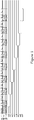
- Figure 1 shows the signals on example prior art SPI bus in which eight slave SPI devices are sequentially polled using active-low chip select signals transmitted on chip select lines cs0 to cs7.
- the sequence includes eight frames, with each frame prompting a selected slave device, from dev_0 to dev_7, to read a refresh signal from the MOSI line and transmit diagnostic data to the MISO line for logging by the master SPI device.
- a problem with the above is that it is relatively slow and requires continuous communication on the SPI bus during the polling sequence. Accordingly, as the number of slave devices increases, more and more processing and SPI bus time is occupied by the refresh operations, reducing the availability of this resource for normal device operation. In addition, it also limits the number of slave devices that may be served by a master device because there may not otherwise be sufficient time between each repeat polling sequence before the watchdog of a particular slave device times-out.
- the present disclosure concerns a communications system for allowing the fast polling of one or more groups of multiple slave integrated circuits command procedures.
- the communication system may be for use within embedded systems in automotive applications.
- a communications system including: a master circuit including a master serial peripheral interface, SPI, device having an input MISO terminal; and a plurality of slave circuits coupled for communication with the master circuit, each includes a slave SPI device, an activation terminal for activating the slave SPI device, and an output switch for connecting an output master-in slave-out, MISO, terminal of the slave SPI device to the input MISO terminal when activated, wherein the master circuit further includes: a polling signal terminal for transmitting a polling signal to the activation terminals of at least a first group of the plurality of slave circuits for activating their respective slave SPI devices; and a plurality of output chip-select, CS, terminals, each independently activatable for transmitting a CS signal to both the activation terminal and the output switch of a respective one of the plurality of slave circuits for activating the respective slave SPI device and connecting its output MISO terminal for transmitting data to the input MISO terminal.
- a polling signal terminal for transmitting a polling signal
- a plurality of slave SPI devices can be refreshed simultaneously by polling them in a single SPI frame, whilst limiting the data returned to the master SPI device to that transmitted by a single slave SPI device.
- watchdog timers in all the slave SPI devices can be rapidly reset to avoid timeout based on a common reset signal transmitted on the MOSI line, whilst diagnostic data from one of the slave SPI devices may still be transmitted back to the master on the MISO line. Importantly, this may be achieved without modification to the SPI clock signal or the operating software of the SPI devices.
- the master circuit further includes a demultiplexer connected to an address terminal provided on the master SPI device, and wherein the plurality of output CS terminals are provided on the demultiplexer and are individually activatable in response to the demultiplexing of the address signal from the address terminal.
- a larger number of slave SPI devices may be controlled using the CS terminals based on a signal output from a single address terminal.
- the communications system further includes a second polling signal terminal for transmitting a second polling signal to the activation terminals of a second group of the plurality of slave circuits for simultaneously activating their respective slave SPI devices.
- a second polling signal terminal for transmitting a second polling signal to the activation terminals of a second group of the plurality of slave circuits for simultaneously activating their respective slave SPI devices.
- the master circuit further includes a polling logic arrangement, wherein the polling signal terminal and the second polling signal terminal are provided on the polling logic arrangement, wherein the polling logic arrangement includes a plurality of logic gates connected to the master polling terminal provided on the master SPI device and the output CS terminals associated with the first and second groups of slave circuits, and wherein the polling logic arrangement is configured for transmitting a polling signal from one of the first and second polling signal terminals in response to both a master polling signal and at least one CS signal associated with a slave circuit in the respective group. In this way, more than one polling signal group of slave SPI devices may be polled using the output of a single polling terminal on the master SPI device.
- the polling signal terminal is further provided on the demultiplexer, and wherein the polling signal terminal is activated based on demultiplexing the address signal from the address terminal.
- a basic master SPI device with only an address terminal may be used to generate both CS signals and polling signals through the demultiplexer.
- the master SPI device includes a serial clock terminal for transmitting a clock signal to the plurality of slave SPI devices.
- the master SPI device includes an output master-out slave-in, MOSI, terminal for transmitting data from the master SPI device to the plurality of slave SPI devices.
- MOSI output master-out slave-in
- the communications system further includes a MOSI line connected between the output MOSI terminal and input MOSI terminals provided on the plurality of slave circuits.
- the communications system further includes a MISO line connected between the input MISO terminal and the output MISO terminals of the plurality of slave circuits; a polling signal line connected between the polling signal terminal and the activation terminals of the plurality of slave circuits; and a plurality of CS signal lines, each connected between one of the plurality of output CS terminals and the activation terminal and output switch of one of the slave circuits.
- a method for operating a communications system including the steps of: providing a master circuit including a polling signal terminal, a plurality of chip-select, CS, terminals, and a master serial peripheral interface, SPI, device having an input MISO terminal and; providing a plurality of slave circuits coupled for communication with the master circuit, each including a slave SPI device, an activation terminal, and an output switch; transmitting a polling signal from the polling signal terminal to the activation terminals of at least a first group of the plurality of slave circuits for activating their respective slave SPI devices, wherein the respective output MISO terminal is prevented from transmitting data to the input MISO terminal by the output switch unless it is activated; and transmitting CS signals from individual ones of the CS terminals to a respective one of the plurality of slave circuits for activating its activation terminal to activate the respective slave SPI device and for activating the output switch to connect its output MISO terminal to the input MISO terminal for transmitting data
- the method further includes transmitting a sequence of SPI frames, wherein each SPI frame includes transmitting a polling signal and a CS signal from one of the CS terminals to a respective slave circuit, wherein the CS signal is transmitted from a different CS terminal in each frame of the sequence of SPI frames for sequentially connecting the respective output MISO terminals of the slave circuits to the input MISO terminal.
- each SPI frame includes transmitting a polling signal and a CS signal from one of the CS terminals to a respective slave circuit
- the CS signal is transmitted from a different CS terminal in each frame of the sequence of SPI frames for sequentially connecting the respective output MISO terminals of the slave circuits to the input MISO terminal.
- the step of providing the master circuit further includes providing a demultiplexer connected to an address terminal provided on the master SPI, wherein the plurality of output CS terminals are provided on the demultiplexer, and wherein the method further includes the steps of: transmitting an address signal from the address terminal to the demultiplexer; demultiplexing the address signal at the demultiplexer; and generating a CS signal from one of the CS terminals for transmission to a respective one of the plurality of slave circuits based on the demultiplexed address signal.
- the step of demultiplexing the address signal includes selecting one of the CS terminals to transmit the CS signal based on one of the address signal's least significant bits or the address signal's most significant bits. In this way, a simple multiplexed signal may be used for addressing to a group of slave devices to be refreshed and an individual slave SPI device for returning data to the master.
- the step of providing a demultiplexer further includes providing the polling signal terminal on the demultiplexer, and wherein the method further includes generating the polling signal from the polling signal terminal based on the demultiplexed address signal.
- the step of demultiplexing the address signal includes selecting to generate a polling signal from the polling signal terminal or a second polling signal from a second polling signal terminal based on one of the address signal's most significant bits or the address signal's least significant bits.
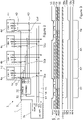
- FIG. 2 shows a communications system 1 according to a first embodiment.
- the communications system 1 includes a master circuit 3 communicatively coupled to four slave circuits 4a-4d.
- the master circuit 3 includes a master SPI device 31 and a demultiplexer 32.
- the master SPI device is provided as an integrated circuit with the SPI address, clock (CLK), MOSI, and MISO terminals.
- the master SPI device 31 further includes a polling terminal for generating a polling signal independent of the address signals.
- the signals transmitted over the SPI bus are active-low signals.
- the address terminal is connected to an input of the demultiplexer 32 via address signal line 52.
- the demultiplexer 32 includes a plurality of output CS terminals, CS_0 to CS_3, associated with each of the slave circuits 4a-4d. As such, a multiplexed address signal transmitted from the address terminal of the master SPI device 31 may be demultiplexed to generate an individual CS address signal in one of the output CS terminals of the demultiplexer 32.
- Each of the four slave circuits 4a-4d includes a slave SPI device 41, together with an AND gate 42 connected to its CS input terminal and an output switch 43 connected to its output MISO terminal.
- Each AND gate 42 is connected to both the output of the polling terminal on the master SPI device 31 via polling signal line 51 and the respective output CS terminal, CS_0 to CS-3, on the demultiplexer 32 via CS signal line 56a-d. In the absence of either a polling signal or an individual chip select signal, both the inputs to the AND gate 42 are high, causing the CS terminal on the respective slave SPI device 41 to be held high. When an active-low signal is applied to either input, the CS terminal on the respective slave SPI device 41 is set low, thereby activating it. Consequently, the slave SPI devices 41 of each slave circuit 4a-d may be activated by either the polling signal or an individual chip select signal applied via its respective CS signal line 56a-d.
- Each output switch 43 is also controlled by the output of the respective output CS terminal on the demultiplexer 32 via CS signal lines 56a-d. As such, when an individual chip select signal is transmitted for activating a respective slave SPI device 41, the associated output switch 43 is switched to connect the respective output MISO terminal to the input MISO terminal on the master SPI device 31 via MISO data line 55.
- MISO data line 55 connects the output switches of each of the slave circuits 4a-4d to the input MISO terminal on the master SPI device 31. Accordingly, data from any of the slave SPI devices 41 may be transmitted to the master SPI device 31, but only when its respective output switch 43 is activated.
- the CLK and MOSI terminals of the master SPI device 31 are connected to the CLK and MOSI terminals of the slave SPI devices 41 via clock signal line 53 and MOSI data line 55 for transmitting clock and data signals.
- FIG 3 shows the signals on the SPI bus during an example polling sequence operating on the system shown in Figure 2 .
- the illustration shows 4 frames 61-64, with polling operations being actioned in frames 61 and 64.
- Frames 62 and 63 represent available bus time where polling operations are not being actioned and hence the SPI bus may be used for other operations.
- the master SPI device 31 In frame 61, the master SPI device 31 outputs a polling signal through its polling terminal as well as a CS address signal through its address terminal to cause the demultiplexer 32 to generate a chip select signal in chip select terminal CS_0 and hence CS signal line 56a.
- the master SPI device 31 also generates a clock signal through the CLK terminal and transmits an input diagnostic signal through the output MOSI terminal.
- the polling signal on polling signal line 51 causes all four slave SPI devices 41 of the slave circuits 4a-d to be activated and to read data from the MOSI data line 54 via polling signal line 51. This thereby prompts the watchdog to reset for avoiding time out of the device.
- only the output switch 43 of the first slave circuit 4a is activated because only the associated CS signal line 56a is carrying a CS signal. Consequently, only the first slave SPI device 41a is able to transmit diagnostic data to the master SPI device 31 on the MISO signal line 55.
- a second refresh operation may be actioned.
- the master SPI device 31 outputs a polling signal through its polling terminal, but in this instance the address signal from the main SPI device 31 causes the demultiplexer 32 to generate a chip select signal in the second chip select terminal CS_1, and hence CS signal line 56b.
- all four slave SPI devices 41 are again activated to read data from the MOSI data line 54, but only the output switch 43 of the second slave circuit 4b is activated. Consequently, for this frame, only the slave SPI device 41 of the second slave circuit 4b is able to transmit diagnostic data on the MISO signal line 55.
- the above process may be repeated for further cycles to obtain diagnostic data from the third and fourth slave circuits 4c and 4d.
- the slave SPI devices 41 can thereby be refreshed in a single frame, albeit that the master SPI device 31 will only receive diagnostic data from one of the slave devices in each refresh cycle. Nevertheless, the diagnostic data is typically less important because the peripheral devices will normally be able to maintain their operation autonomously, and hence are tolerant to a reduction in their feedback rate, provided they can be refreshed regularly.
- conventional SPI data transfer processes may be implemented in frames in which polling operations are not occurring, such as in frames 62 and 63 shown in Figure 3 .
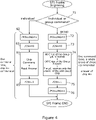
- Figure 4 shows a flow diagram of operations of the system shown in Figure 2 .
- step 71 it is decided whether to implement commands to individual slave circuits or whether to poll the whole group.
- step 74 this causes all the SPI slave device chips of the slave circuits 4a-d to be refreshed and generate an output signal.
- the CS signal line 56 and the polling signal line 51 may then be set back to a logic low state in steps 75 and 76 to end the SPI frame.
- step 82 When the system is commanding a specific slave circuit individually, for example for implementing a configuration operation, no polling signal is applied to the polling signal line 51 in step 82.
- An active-low CS signal is applied to one of the CS signal lines 56a-d in step 83.
- step 84 this then causes the slave SPI device chip of the selected slave circuit 4a-d to read data from the MOSI signal line 54 and generate an output signal on the MISO signal line 55.
- the MOSI signal from the slave SPI device 41 is transmitted back to the master circuit 3.
- the CS signal line 56 may then be set back to a logic low state in step 85 to end the SPI frame. It will be understood that different slave circuits may be activated by generating CS signals in their respective CS signal lines.
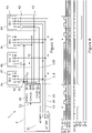
- FIGS 5 and 6 respectively show a schematic illustration and the SPI bus signals according to a second embodiment.
- This embodiment operates in substantially the same way as the first embodiment, with the same reference numerals being used for corresponding features.
- the polling signal terminal, POLLING_GP1 being provided on the master SPI device 31, it is provided on the demultiplexer 32, along with a second polling signal terminal, POLLING_GP_n.
- the first and second polling signal terminals are independently activated based on demultiplexing the CS address signal transmitted on address signal line 52.
- the first polling signal terminal, POLLING_GP_1 is used for polling slave circuits 4a-c simultaneously as a first group of slave devices through first polling signal line 51a.
- the second polling signal terminal, POLLING_GP_n is used for polling slave circuit 4d through second polling signal line 51b. It will be understood that in other embodiments further slave circuits may be included in the second polling groups or further polling groups may be provided by providing further polling signal terminals.
- the system shown in Figure 5 may be operated in the same way as the first embodiment, with the generation of a polling signal being used to simultaneously refresh all slave circuits sharing a common polling signal line 56a-b, with only one of the slave circuits being selected each cycle to return data back to the master SPI device 31.
- a first group including three slave circuits 4a-c or a second group including only slave circuit 4d may be refreshed separately by addressing their respective polling signal terminals. This may thereby allow different slave SPI devices 41 to be refreshed at different rates.
- the address signal generated at the address terminal on the master SPI bus is multiplexed with the address signal's most significant bits being used to initiate a polling signal and designate which group of slave circuits is to be polled by activating the respective polling signal terminal.
- the address signal's least significant bits are used to designate which CS signal terminal is to be activated. It will be understood that other multiplexing protocols may alternatively be used.
- FIG. 7 shows a schematic illustration of a system according to a third embodiment.
- This embodiment operates in substantially the same way as the second embodiment, with the same reference numerals being used for corresponding features.
- five slave devices 4a-e are provided, and a single polling signal terminal on the master SPI device 31 is used to generate both the first and second polling signals via a combination of additional AND and OR gates.
- the master circuit 31 further includes first and second OR gates 34a,34b for generating the first and second polling signals.
- Each OR gate 34a,34b is connected to the polling signal terminal of the master SPI device 31 via polling input 51i, as well as all of the respective CS signal lines 56a-e corresponding to the slave circuits 4a-e in their group.
- a polling AND gate 33a is connected to each of CS signal lines 56a-c. As such, if an active-low signal is applied on any of CS signal lines 56a-c, an active low signal is output from the polling AND gate 33a, and fed to the OR gate 34a.
- the second polling group contains the fourth and fifth slave circuits 4d-e and therefore its polling AND gate 33b is connected to each of CS signal lines 56d-e. Again, if an active-low signal is applied on either of CS signal lines 56d-e, an active low signal is output from its polling AND gate 33b, and fed to the respective OR gate 34b.
- the first and second OR gates 34a,34b maintain a high (logic low) signal when either the polling input 51i or their respective CS signal lines 56a-d are held high (logic low).
- an active-low signal is applied by both the polling input 51i and one of CS signal lines 56a-c for the first polling group (first OR gate 34a) or one of CS signal line 56d-e for the second polling group (second OR gate 34b)
- an active-low polling signal is output by the respective OR gate 34a,34b for activating all the slave SPI devices 41 in the respective group, as with the second embodiment.
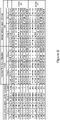
- Figure 8 shows a logic table summarising the operations of the system shown in Figure 7 . It will also be understood that other embodiments may include further slave circuits in either of the polling groups, as well as further polling groups.
- Figure 9 shows the connections and integrated logic devices at each of the slave circuits.
- the right-hand side shows the inputs to each slave SPI device 41.
- the AND gates 42 output to the CS terminal of the slave SPI device 41 and receive inputs from a respective CS signal line 56 as well as the polling signal line 51 for the respective group.
- the AND gates may be implemented using an open-drain 74hc09 integrated circuit.
- the MOSI signal line 54 and the clock signal line 53 connect between the respective terminals on the master SPI device 31 and the slave SPI devices 41.
- the output switch 43 is provided in the MISO signal line 55 and is switched by the respective CS signal line 56. In embodiments, the output switch 43 may be implemented using a 74hc125 integrated circuit.
- Figure 10 shows an illustrative discrete implementation of two AND gates 42 for controlling the activation of two slave SPI devices 41.
- the above arrangements allow for the fast polling of multiple slave SPI devices within a single SPI frame, thereby allowing their watchdog timers to be reset to prevent inadvertent time outs.
- the use of SPI frames for refresh cycles is minimised, freeing time on the SPI bus for other operations.
- the arrangement may allow for the use of standard SPI integrated circuits since it does not require modification of the SPI clock signal or significant additional CS control signals, or the use of non-standard software. This thereby minimises costs as off the shelf components may be used.
- the CS signal terminals are provided on the demultiplexer, in other embodiments, no demultiplexer is required.
- the CS signal terminals may be incorporated into the master SPI device.
- the above illustrative examples describe arrangements which allow all the slave devices in a group to be activated in the same SPI command frame for the purpose of refreshing their watchdogs.
- the arrangement may also be used for commands. That is, the whole group of slave devices can be turned on and instructed in the same command frame, thereby allowing those devices to simultaneously receive commands from the master device. This may be implemented using the group command steps 72-76 shown in Figure 4 .
Landscapes
- Engineering & Computer Science (AREA)
- Theoretical Computer Science (AREA)
- General Engineering & Computer Science (AREA)
- Physics & Mathematics (AREA)
- General Physics & Mathematics (AREA)
- Computer Hardware Design (AREA)
- Small-Scale Networks (AREA)
- Health & Medical Sciences (AREA)
- Cardiology (AREA)
- General Health & Medical Sciences (AREA)
- Computer Networks & Wireless Communication (AREA)
- Signal Processing (AREA)
Abstract
Description
- The present disclosure relates to a communications system and a method of operating the same. The present disclosure is particularly relevant to a communication apparatus using a serial peripheral interface (SPI) protocol, and most particularly for data transmission circuits in automotive applications.
- SPI is one of the most common communication protocols used for communications in embedded electronics systems within a vehicle. SPI employs a master-slave architecture in which one master supports communications with one or more slave devices. During operation, the master device initiates a frame to action a read/write operation with a selected slave SPI device, with the slave device being selected using a slave or chip select (CS) signal. This prompts the selected slave device to read data from the master-out slave-in (MOSI) signal line and to write data to the master-in slave-out (MISO) signal line, with the reading and writing of bits being coordinated by a clock signal (CLK).
- Within modern vehicles, it is common for a number of devices to require a regular refresh signal to maintain their operation. For example, peripheral devices, such as smart fuses or sensor units, may include a watchdog which needs polling to prevent an unintended time out. Under a standard SPI protocol, it is therefore necessary to have the master device initiate a separate frame to refresh each slave device.
-
Figure 1 shows the signals on example prior art SPI bus in which eight slave SPI devices are sequentially polled using active-low chip select signals transmitted on chip select lines cs0 to cs7. As such, the sequence includes eight frames, with each frame prompting a selected slave device, from dev_0 to dev_7, to read a refresh signal from the MOSI line and transmit diagnostic data to the MISO line for logging by the master SPI device. - A problem with the above is that it is relatively slow and requires continuous communication on the SPI bus during the polling sequence. Accordingly, as the number of slave devices increases, more and more processing and SPI bus time is occupied by the refresh operations, reducing the availability of this resource for normal device operation. In addition, it also limits the number of slave devices that may be served by a master device because there may not otherwise be sufficient time between each repeat polling sequence before the watchdog of a particular slave device times-out.
- Recently, there has been proposed a number of new SPI based communication systems which seek to address the more general problem of increasing SPI communication speed. For example, it has been proposed to modify the standard SPI protocol to allow different slave devices to communicate within the same frame either by modifying the clock signal or by providing dedicated chip select lines for controlling each slave's MOSI and MISO terminals. However, such arrangements are very complex and require specialised custom hardware, which are significantly more expensive than standard or off-the-shelf SPI integrated circuits. As such, they are not suitable for addressing the above problem associated with refreshing peripheral devices for commercial automotive applications.
- There is therefore a need to address the above problems associated with conventional SPI communication systems in a cost effective and simple manner.
- The present disclosure concerns a communications system for allowing the fast polling of one or more groups of multiple slave integrated circuits command procedures. The communication system may be for use within embedded systems in automotive applications.
- According to a first aspect, there is provided a communications system, including: a master circuit including a master serial peripheral interface, SPI, device having an input MISO terminal; and a plurality of slave circuits coupled for communication with the master circuit, each includes a slave SPI device, an activation terminal for activating the slave SPI device, and an output switch for connecting an output master-in slave-out, MISO, terminal of the slave SPI device to the input MISO terminal when activated, wherein the master circuit further includes: a polling signal terminal for transmitting a polling signal to the activation terminals of at least a first group of the plurality of slave circuits for activating their respective slave SPI devices; and a plurality of output chip-select, CS, terminals, each independently activatable for transmitting a CS signal to both the activation terminal and the output switch of a respective one of the plurality of slave circuits for activating the respective slave SPI device and connecting its output MISO terminal for transmitting data to the input MISO terminal.
- In this way, a plurality of slave SPI devices can be refreshed simultaneously by polling them in a single SPI frame, whilst limiting the data returned to the master SPI device to that transmitted by a single slave SPI device. As such, watchdog timers in all the slave SPI devices can be rapidly reset to avoid timeout based on a common reset signal transmitted on the MOSI line, whilst diagnostic data from one of the slave SPI devices may still be transmitted back to the master on the MISO line. Importantly, this may be achieved without modification to the SPI clock signal or the operating software of the SPI devices.
- In embodiments, the master circuit further includes a demultiplexer connected to an address terminal provided on the master SPI device, and wherein the plurality of output CS terminals are provided on the demultiplexer and are individually activatable in response to the demultiplexing of the address signal from the address terminal. In this way, a larger number of slave SPI devices may be controlled using the CS terminals based on a signal output from a single address terminal.
- In embodiments, the communications system further includes a second polling signal terminal for transmitting a second polling signal to the activation terminals of a second group of the plurality of slave circuits for simultaneously activating their respective slave SPI devices. In this way, more than one group of slave SPI devices may be polled, thereby allowing different groups to be polled at different intervals as needed. Furthermore, different groups of slave SPI devices which are responsive to different commands on the MOSI line may be instructed separately as a discrete group.
- In embodiments, the master circuit further includes a polling logic arrangement, wherein the polling signal terminal and the second polling signal terminal are provided on the polling logic arrangement, wherein the polling logic arrangement includes a plurality of logic gates connected to the master polling terminal provided on the master SPI device and the output CS terminals associated with the first and second groups of slave circuits, and wherein the polling logic arrangement is configured for transmitting a polling signal from one of the first and second polling signal terminals in response to both a master polling signal and at least one CS signal associated with a slave circuit in the respective group. In this way, more than one polling signal group of slave SPI devices may be polled using the output of a single polling terminal on the master SPI device.
- In embodiments, the polling signal terminal is further provided on the demultiplexer, and wherein the polling signal terminal is activated based on demultiplexing the address signal from the address terminal. In this way, a basic master SPI device with only an address terminal may be used to generate both CS signals and polling signals through the demultiplexer.
- In embodiments, the master SPI device includes a serial clock terminal for transmitting a clock signal to the plurality of slave SPI devices.
- In embodiments, the master SPI device includes an output master-out slave-in, MOSI, terminal for transmitting data from the master SPI device to the plurality of slave SPI devices.
- In embodiments, the communications system further includes a MOSI line connected between the output MOSI terminal and input MOSI terminals provided on the plurality of slave circuits.
- In embodiments, the communications system further includes a MISO line connected between the input MISO terminal and the output MISO terminals of the plurality of slave circuits; a polling signal line connected between the polling signal terminal and the activation terminals of the plurality of slave circuits; and a plurality of CS signal lines, each connected between one of the plurality of output CS terminals and the activation terminal and output switch of one of the slave circuits.
- According to a second aspect, there is provided a method for operating a communications system, the method including the steps of: providing a master circuit including a polling signal terminal, a plurality of chip-select, CS, terminals, and a master serial peripheral interface, SPI, device having an input MISO terminal and; providing a plurality of slave circuits coupled for communication with the master circuit, each including a slave SPI device, an activation terminal, and an output switch; transmitting a polling signal from the polling signal terminal to the activation terminals of at least a first group of the plurality of slave circuits for activating their respective slave SPI devices, wherein the respective output MISO terminal is prevented from transmitting data to the input MISO terminal by the output switch unless it is activated; and transmitting CS signals from individual ones of the CS terminals to a respective one of the plurality of slave circuits for activating its activation terminal to activate the respective slave SPI device and for activating the output switch to connect its output MISO terminal to the input MISO terminal for transmitting data thereto.
- In embodiments, the method further includes transmitting a sequence of SPI frames, wherein each SPI frame includes transmitting a polling signal and a CS signal from one of the CS terminals to a respective slave circuit, wherein the CS signal is transmitted from a different CS terminal in each frame of the sequence of SPI frames for sequentially connecting the respective output MISO terminals of the slave circuits to the input MISO terminal. In this way, diagnostic data from each of the slave SPI devices may be fed back to the master SPI device over a number of refresh cycles.
- In embodiments, wherein the step of providing the master circuit further includes providing a demultiplexer connected to an address terminal provided on the master SPI, wherein the plurality of output CS terminals are provided on the demultiplexer, and wherein the method further includes the steps of: transmitting an address signal from the address terminal to the demultiplexer; demultiplexing the address signal at the demultiplexer; and generating a CS signal from one of the CS terminals for transmission to a respective one of the plurality of slave circuits based on the demultiplexed address signal.
- In embodiments, wherein the step of demultiplexing the address signal includes selecting one of the CS terminals to transmit the CS signal based on one of the address signal's least significant bits or the address signal's most significant bits. In this way, a simple multiplexed signal may be used for addressing to a group of slave devices to be refreshed and an individual slave SPI device for returning data to the master.
- In embodiments, the step of providing a demultiplexer further includes providing the polling signal terminal on the demultiplexer, and wherein the method further includes generating the polling signal from the polling signal terminal based on the demultiplexed address signal.
- In embodiments, the step of demultiplexing the address signal includes selecting to generate a polling signal from the polling signal terminal or a second polling signal from a second polling signal terminal based on one of the address signal's most significant bits or the address signal's least significant bits.
- Illustrative embodiments will now be described with reference to the accompanying drawings in which:
-
Figure 1 shows the signals on an example prior art SPI bus; -
Figure 2 shows a schematic illustration of a communications system according to a first embodiment; -
Figure 3 shows the signals on the SPI bus during a polling sequence operating on the system shown inFigure 2 ; -
Figure 4 shows a flow diagram of operations of the system shown inFigure 2 ; -
Figure 5 shows a schematic illustration of a communications system according to a second embodiment; -
Figure 6 shows the signals on the SPI bus during a polling sequence operating on the system shown inFigure 5 ; -
Figure 7 shows a schematic illustration of a communications system according to a third embodiment; -
Figure 8 shows an illustrative logic table for operations of the system shown inFigure 7 ; -
Figure 9 shows the connections and integrated logic devices at each of the slave circuits; and -
Figure 10 shows an example discrete implementation alternative to the integrated AND gate shown inFigure 10 . -
Figure 2 shows acommunications system 1 according to a first embodiment. Thecommunications system 1 includes amaster circuit 3 communicatively coupled to fourslave circuits 4a-4d. - The
master circuit 3 includes amaster SPI device 31 and ademultiplexer 32. The master SPI device is provided as an integrated circuit with the SPI address, clock (CLK), MOSI, and MISO terminals. Themaster SPI device 31 further includes a polling terminal for generating a polling signal independent of the address signals. The signals transmitted over the SPI bus are active-low signals. - The address terminal is connected to an input of the
demultiplexer 32 viaaddress signal line 52. Thedemultiplexer 32 includes a plurality of output CS terminals, CS_0 to CS_3, associated with each of theslave circuits 4a-4d. As such, a multiplexed address signal transmitted from the address terminal of themaster SPI device 31 may be demultiplexed to generate an individual CS address signal in one of the output CS terminals of thedemultiplexer 32. - Each of the four
slave circuits 4a-4d includes aslave SPI device 41, together with an ANDgate 42 connected to its CS input terminal and anoutput switch 43 connected to its output MISO terminal. - Each AND
gate 42 is connected to both the output of the polling terminal on themaster SPI device 31 viapolling signal line 51 and the respective output CS terminal, CS_0 to CS-3, on thedemultiplexer 32 viaCS signal line 56a-d. In the absence of either a polling signal or an individual chip select signal, both the inputs to the ANDgate 42 are high, causing the CS terminal on the respectiveslave SPI device 41 to be held high. When an active-low signal is applied to either input, the CS terminal on the respectiveslave SPI device 41 is set low, thereby activating it. Consequently, theslave SPI devices 41 of eachslave circuit 4a-d may be activated by either the polling signal or an individual chip select signal applied via its respectiveCS signal line 56a-d. - Each
output switch 43 is also controlled by the output of the respective output CS terminal on thedemultiplexer 32 viaCS signal lines 56a-d. As such, when an individual chip select signal is transmitted for activating a respectiveslave SPI device 41, the associatedoutput switch 43 is switched to connect the respective output MISO terminal to the input MISO terminal on themaster SPI device 31 viaMISO data line 55. -
MISO data line 55 connects the output switches of each of theslave circuits 4a-4d to the input MISO terminal on themaster SPI device 31. Accordingly, data from any of theslave SPI devices 41 may be transmitted to themaster SPI device 31, but only when itsrespective output switch 43 is activated. - The CLK and MOSI terminals of the
master SPI device 31 are connected to the CLK and MOSI terminals of theslave SPI devices 41 viaclock signal line 53 and MOSIdata line 55 for transmitting clock and data signals. -
Figure 3 shows the signals on the SPI bus during an example polling sequence operating on the system shown inFigure 2 . The illustration shows 4 frames 61-64, with polling operations being actioned inframes Frames - In
frame 61, themaster SPI device 31 outputs a polling signal through its polling terminal as well as a CS address signal through its address terminal to cause thedemultiplexer 32 to generate a chip select signal in chip select terminal CS_0 and henceCS signal line 56a. Themaster SPI device 31 also generates a clock signal through the CLK terminal and transmits an input diagnostic signal through the output MOSI terminal. - The polling signal on
polling signal line 51 causes all fourslave SPI devices 41 of theslave circuits 4a-d to be activated and to read data from theMOSI data line 54 viapolling signal line 51. This thereby prompts the watchdog to reset for avoiding time out of the device. At the same time, only theoutput switch 43 of thefirst slave circuit 4a is activated because only the associatedCS signal line 56a is carrying a CS signal. Consequently, only the first slave SPI device 41a is able to transmit diagnostic data to themaster SPI device 31 on theMISO signal line 55. - In
frame 64, a second refresh operation may be actioned. Again, themaster SPI device 31 outputs a polling signal through its polling terminal, but in this instance the address signal from themain SPI device 31 causes thedemultiplexer 32 to generate a chip select signal in the second chip select terminal CS_1, and henceCS signal line 56b. Accordingly, all fourslave SPI devices 41 are again activated to read data from theMOSI data line 54, but only theoutput switch 43 of thesecond slave circuit 4b is activated. Consequently, for this frame, only theslave SPI device 41 of thesecond slave circuit 4b is able to transmit diagnostic data on theMISO signal line 55. - The above process may be repeated for further cycles to obtain diagnostic data from the third and
fourth slave circuits - With the above arrangement, all of the
slave SPI devices 41 can thereby be refreshed in a single frame, albeit that themaster SPI device 31 will only receive diagnostic data from one of the slave devices in each refresh cycle. Nevertheless, the diagnostic data is typically less important because the peripheral devices will normally be able to maintain their operation autonomously, and hence are tolerant to a reduction in their feedback rate, provided they can be refreshed regularly. - Importantly, with the arrangement shown in
Figure 2 , conventional SPI data transfer processes may be implemented in frames in which polling operations are not occurring, such as inframes Figure 3 . - In this respect,
Figure 4 shows a flow diagram of operations of the system shown inFigure 2 . For each SPI frame, instep 71, it is decided whether to implement commands to individual slave circuits or whether to poll the whole group. - When a polling operation is selected to refresh the
slave circuits 4a-d, this proceeds as discussed above with an active-low polling signal being applied to thepolling signal line 51 instep 72, and an active-low CS signal being applied to one of the CS signal lines 56 instep 73. Instep 74, this causes all the SPI slave device chips of theslave circuits 4a-d to be refreshed and generate an output signal. However, only theslave circuit 4a-d selected by the CS signal is transmitted back to themaster circuit 3. The CS signal line 56 and thepolling signal line 51 may then be set back to a logic low state insteps - When the system is commanding a specific slave circuit individually, for example for implementing a configuration operation, no polling signal is applied to the
polling signal line 51 instep 82. An active-low CS signal is applied to one of theCS signal lines 56a-d instep 83. Instep 84, this then causes the slave SPI device chip of the selectedslave circuit 4a-d to read data from theMOSI signal line 54 and generate an output signal on theMISO signal line 55. As the associatedoutput switch 43 is activated, the MOSI signal from theslave SPI device 41 is transmitted back to themaster circuit 3. The CS signal line 56 may then be set back to a logic low state instep 85 to end the SPI frame. It will be understood that different slave circuits may be activated by generating CS signals in their respective CS signal lines. -
Figures 5 and 6 respectively show a schematic illustration and the SPI bus signals according to a second embodiment. This embodiment operates in substantially the same way as the first embodiment, with the same reference numerals being used for corresponding features. In this embodiment, however, rather than the polling signal terminal, POLLING_GP1, being provided on themaster SPI device 31, it is provided on thedemultiplexer 32, along with a second polling signal terminal, POLLING_GP_n. The first and second polling signal terminals are independently activated based on demultiplexing the CS address signal transmitted onaddress signal line 52. The first polling signal terminal, POLLING_GP_1, is used for pollingslave circuits 4a-c simultaneously as a first group of slave devices through firstpolling signal line 51a. The second polling signal terminal, POLLING_GP_n, is used for pollingslave circuit 4d through secondpolling signal line 51b. It will be understood that in other embodiments further slave circuits may be included in the second polling groups or further polling groups may be provided by providing further polling signal terminals. - As shown in
Figure 6 , the system shown inFigure 5 may be operated in the same way as the first embodiment, with the generation of a polling signal being used to simultaneously refresh all slave circuits sharing a commonpolling signal line 56a-b, with only one of the slave circuits being selected each cycle to return data back to themaster SPI device 31. As such, in this embodiment, a first group including threeslave circuits 4a-c or a second group includingonly slave circuit 4d may be refreshed separately by addressing their respective polling signal terminals. This may thereby allow differentslave SPI devices 41 to be refreshed at different rates. - In this embodiment, the address signal generated at the address terminal on the master SPI bus is multiplexed with the address signal's most significant bits being used to initiate a polling signal and designate which group of slave circuits is to be polled by activating the respective polling signal terminal. The address signal's least significant bits are used to designate which CS signal terminal is to be activated. It will be understood that other multiplexing protocols may alternatively be used.
-
Figure 7 shows a schematic illustration of a system according to a third embodiment. This embodiment operates in substantially the same way as the second embodiment, with the same reference numerals being used for corresponding features. However, in this embodiment, fiveslave devices 4a-e are provided, and a single polling signal terminal on themaster SPI device 31 is used to generate both the first and second polling signals via a combination of additional AND and OR gates. - In this connection, the
master circuit 31 further includes first and second ORgates gate master SPI device 31 viapolling input 51i, as well as all of the respectiveCS signal lines 56a-e corresponding to theslave circuits 4a-e in their group. To facilitate this for the first polling group includingslave circuits 4a-c, a polling ANDgate 33a is connected to each ofCS signal lines 56a-c. As such, if an active-low signal is applied on any ofCS signal lines 56a-c, an active low signal is output from the polling ANDgate 33a, and fed to theOR gate 34a. Similarly, the second polling group contains the fourth andfifth slave circuits 4d-e and therefore its polling AND gate 33b is connected to each ofCS signal lines 56d-e. Again, if an active-low signal is applied on either ofCS signal lines 56d-e, an active low signal is output from its polling AND gate 33b, and fed to the respective ORgate 34b. - With the above arrangement, the first and second OR
gates polling input 51i or their respectiveCS signal lines 56a-d are held high (logic low). However, if an active-low signal is applied by both thepolling input 51i and one ofCS signal lines 56a-c for the first polling group (first ORgate 34a) or one ofCS signal line 56d-e for the second polling group (second ORgate 34b), an active-low polling signal is output by the respective ORgate slave SPI devices 41 in the respective group, as with the second embodiment.Figure 8 shows a logic table summarising the operations of the system shown inFigure 7 . It will also be understood that other embodiments may include further slave circuits in either of the polling groups, as well as further polling groups. -
Figure 9 shows the connections and integrated logic devices at each of the slave circuits. The right-hand side shows the inputs to eachslave SPI device 41. As shown, the ANDgates 42 output to the CS terminal of theslave SPI device 41 and receive inputs from a respective CS signal line 56 as well as thepolling signal line 51 for the respective group. In embodiments, the AND gates may be implemented using an open-drain 74hc09 integrated circuit. TheMOSI signal line 54 and theclock signal line 53 connect between the respective terminals on themaster SPI device 31 and theslave SPI devices 41. Theoutput switch 43 is provided in theMISO signal line 55 and is switched by the respective CS signal line 56. In embodiments, theoutput switch 43 may be implemented using a 74hc125 integrated circuit. - It will be understood that embodiments may use discrete implementations for the AND
gates 42 andoutput switches 43, rather than utilising integrated circuits. For example,Figure 10 shows an illustrative discrete implementation of two ANDgates 42 for controlling the activation of twoslave SPI devices 41. - It will be understood that the above arrangements allow for the fast polling of multiple slave SPI devices within a single SPI frame, thereby allowing their watchdog timers to be reset to prevent inadvertent time outs. As such, the use of SPI frames for refresh cycles is minimised, freeing time on the SPI bus for other operations. At the same time, the arrangement may allow for the use of standard SPI integrated circuits since it does not require modification of the SPI clock signal or significant additional CS control signals, or the use of non-standard software. This thereby minimises costs as off the shelf components may be used.
- It will be understood that the embodiments illustrated above shows applications only for the purposes of illustration. In practice, embodiments may be applied to many different configurations, the detailed embodiments being straightforward for those skilled in the art to implement.
- In this connection, for example, it will be understood that whilst in the above embodiments the CS signal terminals are provided on the demultiplexer, in other embodiments, no demultiplexer is required. For example, the CS signal terminals may be incorporated into the master SPI device.
- Furthermore, the above illustrative examples describe arrangements which allow all the slave devices in a group to be activated in the same SPI command frame for the purpose of refreshing their watchdogs. However, it will be understood that the arrangement may also be used for commands. That is, the whole group of slave devices can be turned on and instructed in the same command frame, thereby allowing those devices to simultaneously receive commands from the master device. This may be implemented using the group command steps 72-76 shown in
Figure 4 .
Claims (15)
- A communications system, comprising:a master circuit comprising a master serial peripheral interface, SPI, device having an input MISO terminal; anda plurality of slave circuits coupled for communication with the master circuit, each comprising a slave SPI device, an activation terminal for activating the slave SPI device, and an output switch for connecting a MISO terminal of the slave SPI device to the input MISO terminal when activated,wherein the master circuit further comprises:a polling signal terminal for transmitting a polling signal to the activation terminals of at least a first group of the plurality of slave circuits for activating their respective slave SPI devices; anda plurality of output chip-select, CS, terminals, each independently activatable for transmitting a CS signal to both the activation terminal and the output switch of a respective one of the plurality of slave circuits for activating the respective slave SPI device and connecting its output MISO terminal for transmitting data to the input MISO terminal.
- A communications system according to claim 1, wherein the master circuit further comprises a demultiplexer connected to an address terminal provided on the master SPI device, and wherein the plurality of output CS terminals are provided on the demultiplexer and are individually activatable in response to the demultiplexing of the address signal from the address terminal.
- A communications system according to any preceding claim, further comprising a second polling signal terminal for transmitting a second polling signal to the activation terminals of a second group of the plurality of slave circuits for simultaneously activating their respective slave SPI devices.
- A communications system according to claim 3, wherein the master circuit further comprises a polling logic arrangement, wherein the polling signal terminal and the second polling signal terminal are provided on the polling logic arrangement,wherein the polling logic arrangement comprises a plurality of logic gates connected to the master polling terminal provided on the master SPI device and the output CS terminals associated with the first and second groups of slave circuits, andwherein the polling logic arrangement is configured to transmit a polling signal from one of the first and second polling signal terminals in response to both a master polling signal and at least one CS signal associated with a slave circuit in the respective group.
- A communications system according to any one of claims 1 to 3, wherein the polling signal terminal is further provided on the demultiplexer, and wherein the polling signal terminal is activated based on demultiplexing the address signal from the address terminal.
- A communications system according to any preceding claim, wherein the master SPI device comprises a clock terminal for transmitting a clock signal to the plurality of slave SPI devices.
- A communications system according to any preceding claim, wherein the master SPI device comprises an output MOSI terminal for transmitting data from the master SPI device to the plurality of slave SPI devices.
- A communications system according to claim 7, further comprising:
a MOSI line connected between the output MOSI terminal and input MOSI terminals provided on the plurality of slave circuits. - A communications system according to any preceding claim, further comprising:a MISO line connected between the input MISO terminal and the output MISO terminals of the plurality of slave circuits;a polling signal line connected between the polling signal terminal and the activation terminals of the plurality of slave circuits; anda plurality of CS signal lines, each connected between one of the plurality of output CS terminals and the activation terminal and output switch of one of the slave circuits.
- A method for operating a communications system, comprising:providing a master circuit comprising a polling signal terminal, a plurality of CS terminals, and a master serial peripheral interface, SPI, device having an input MISO terminal and;providing a plurality of slave circuits coupled for communication with the master circuit, each comprising a slave SPI device, an activation terminal, and an output switch;transmitting a polling signal from the polling signal terminal to the activation terminals of at least a first group of the plurality of slave circuits for activating their respective slave SPI devices, wherein the respective output MISO terminal is prevented from transmitting data to the input MISO terminal by the output switch unless it is activated; andtransmitting CS signals from individual ones of the CS terminals to a respective one of the plurality of slave circuits for activating its activation terminal to activate the respective slave SPI device and for activating the output switch to connect its output MISO terminal to the input MISO terminal for transmitting data thereto.
- A method according to claim 10, further comprising transmitting a sequence of SPI frames, wherein each SPI frame comprises transmitting a polling signal and a CS signal from one of the CS terminals to a respective slave circuit, wherein the CS signal is transmitted from a different CS terminal in each frame of the sequence of SPI frames for sequentially connecting the respective output MISO terminals of the slave circuits to the input MISO terminal.
- A method according to claim 10, wherein the step of providing the master circuit further comprises providing a demultiplexer connected to an address terminal provided on the master SPI, wherein the plurality of output CS terminals are provided on the demultiplexer, and
wherein the method further comprises the steps of:transmitting an address signal from the address terminal to the demultiplexer;demultiplexing the address signal at the demultiplexer; andgenerating a CS signal from one of the CS terminals for transmission to a respective one of the plurality of slave circuits based on the demultiplexed address signal. - A method according to claim 12, wherein the step of demultiplexing the address signal comprises selecting one of the CS terminals to transmit the CS signal based on one of the address signal's least significant bits or the address signal's most significant bits.
- A method according to claim 12 or 13, wherein the step of providing a demultiplexer further comprises providing the polling signal terminal on the demultiplexer, and
wherein the method further comprises generating the polling signal from the polling signal terminal based on the demultiplexed address signal. - A method according to claim 14, wherein the step of demultiplexing the address signal comprises selecting to generate a polling signal from the polling signal terminal or a second polling signal from a second polling signal terminal based on one of the address signal's most significant bits or the address signal's least significant bits.
Priority Applications (3)
| Application Number | Priority Date | Filing Date | Title |
|---|---|---|---|
| EP21153009.2A EP4033370B1 (en) | 2021-01-22 | 2021-01-22 | Communications system and method of operating the same |
| US17/648,417 US12182058B2 (en) | 2021-01-22 | 2022-01-19 | Communications system and method of operating the same |
| CN202210065104.5A CN114817108B (en) | 2021-01-22 | 2022-01-20 | Communication system and method of operating the same |
Applications Claiming Priority (1)
| Application Number | Priority Date | Filing Date | Title |
|---|---|---|---|
| EP21153009.2A EP4033370B1 (en) | 2021-01-22 | 2021-01-22 | Communications system and method of operating the same |
Publications (2)
| Publication Number | Publication Date |
|---|---|
| EP4033370A1 true EP4033370A1 (en) | 2022-07-27 |
| EP4033370B1 EP4033370B1 (en) | 2023-11-15 |
Family
ID=74215720
Family Applications (1)
| Application Number | Title | Priority Date | Filing Date |
|---|---|---|---|
| EP21153009.2A Active EP4033370B1 (en) | 2021-01-22 | 2021-01-22 | Communications system and method of operating the same |
Country Status (3)
| Country | Link |
|---|---|
| US (1) | US12182058B2 (en) |
| EP (1) | EP4033370B1 (en) |
| CN (1) | CN114817108B (en) |
Families Citing this family (1)
| Publication number | Priority date | Publication date | Assignee | Title |
|---|---|---|---|---|
| CN112153278B (en) * | 2019-06-28 | 2022-07-12 | 华为技术有限公司 | Data transmission system based on SPI |
Citations (2)
| Publication number | Priority date | Publication date | Assignee | Title |
|---|---|---|---|---|
| US20080183928A1 (en) * | 2007-01-29 | 2008-07-31 | Microsemi Corp. - Analog Mixed Signal Group Ltd. | Addressable Serial Peripheral Interface |
| US20090022255A1 (en) * | 2003-11-05 | 2009-01-22 | Hitachi, Ltd. | Communication System, Real-Time Control Device, and Information Processing System |
Family Cites Families (21)
| Publication number | Priority date | Publication date | Assignee | Title |
|---|---|---|---|---|
| US7533106B2 (en) * | 2005-09-09 | 2009-05-12 | Quickfilter Technologies, Inc. | Data structures and circuit for multi-channel data transfers using a serial peripheral interface |
| CN100468378C (en) | 2005-12-17 | 2009-03-11 | 鸿富锦精密工业(深圳)有限公司 | SPI device communication circuit |
| DE102007024737A1 (en) * | 2007-05-25 | 2008-11-27 | Robert Bosch Gmbh | Data transfer method between master and slave devices |
| CN101436170A (en) | 2007-11-12 | 2009-05-20 | 鸿富锦精密工业(深圳)有限公司 | SPI equipment communication circuit |
| CN101582823B (en) * | 2008-05-13 | 2012-09-05 | 深圳迈瑞生物医疗电子股份有限公司 | Communicated method, communication system and communication routing device based on SPI bus |
| CN102023942B (en) | 2009-09-09 | 2012-10-10 | 鸿富锦精密工业(深圳)有限公司 | SPI (Serial Peripheral Interface) peripheral access device and method |
| US20110078350A1 (en) | 2009-09-30 | 2011-03-31 | Via Technologies, Inc. | Method for generating multiple serial bus chip selects using single chip select signal and modulation of clock signal frequency |
| TWI406135B (en) | 2010-03-09 | 2013-08-21 | Nuvoton Technology Corp | Data transmission systems and programmable serial peripheral interface controller |
| KR20120055034A (en) | 2010-11-22 | 2012-05-31 | 삼성전자주식회사 | Apparatus for connecting peripheral device in portable terminal using serial peripheral interface and method for transmitting data |
| CN102262604B (en) * | 2011-07-25 | 2017-04-26 | 中兴通讯股份有限公司 | Concurrent access method, system and interface device |
| CN102929820A (en) | 2011-12-30 | 2013-02-13 | 广东佳和通信技术有限公司 | SPI communication device compatible with single/dual wires and communication method thereof |
| US9176919B2 (en) | 2012-06-06 | 2015-11-03 | Honeywell International Inc. | Process controller having multi-channel serial communications link |
| CN105993008A (en) | 2013-11-25 | 2016-10-05 | 株式会社村田制作所 | High-frequency device and method for controlling same |
| DE102014209625B4 (en) | 2014-05-21 | 2016-01-07 | Technisat Digital Gmbh | Transferring the characters of a character string from a first electronic module into a second electronic module |
| PL3001323T3 (en) * | 2014-09-26 | 2018-01-31 | Oberthur Technologies | Serial peripheral interface |
| EP3026570A1 (en) * | 2014-11-28 | 2016-06-01 | Gemalto Sa | A communication system comprising a full-duplex interface with a mechanism to initiate a data exchange |
| US10055376B1 (en) | 2015-01-15 | 2018-08-21 | Maxim Integrated Products, Inc. | Serial peripheral interface system with slave expander |
| WO2016189578A1 (en) | 2015-05-22 | 2016-12-01 | 三菱電機株式会社 | Communication apparatus and power conversion apparatus |
| JP6816765B2 (en) * | 2016-04-19 | 2021-01-20 | 日本精機株式会社 | Vehicle display device |
| FR3068797B1 (en) * | 2017-07-04 | 2019-07-19 | STMicroelectronics (Grand Ouest) SAS | METHOD OF COMMUNICATION BETWEEN A MASTER DEVICE AND N SLAVES CONNECTED ON A SYNCHRONOUS DATA BUS OF THE SPI TYPE AND CORRESPONDING DEVICE |
| TWI666553B (en) | 2018-03-13 | 2019-07-21 | 緯穎科技服務股份有限公司 | Dual way communication method, system, and master device thereof |
-
2021
- 2021-01-22 EP EP21153009.2A patent/EP4033370B1/en active Active
-
2022
- 2022-01-19 US US17/648,417 patent/US12182058B2/en active Active
- 2022-01-20 CN CN202210065104.5A patent/CN114817108B/en active Active
Patent Citations (2)
| Publication number | Priority date | Publication date | Assignee | Title |
|---|---|---|---|---|
| US20090022255A1 (en) * | 2003-11-05 | 2009-01-22 | Hitachi, Ltd. | Communication System, Real-Time Control Device, and Information Processing System |
| US20080183928A1 (en) * | 2007-01-29 | 2008-07-31 | Microsemi Corp. - Analog Mixed Signal Group Ltd. | Addressable Serial Peripheral Interface |
Also Published As
| Publication number | Publication date |
|---|---|
| CN114817108B (en) | 2024-08-30 |
| CN114817108A (en) | 2022-07-29 |
| US20220239579A1 (en) | 2022-07-28 |
| US12182058B2 (en) | 2024-12-31 |
| EP4033370B1 (en) | 2023-11-15 |
Similar Documents
| Publication | Publication Date | Title |
|---|---|---|
| US6842436B2 (en) | Multiport-RAM memory device | |
| US5583754A (en) | Method and device for configuring functional units in a serial master-slave arrangement | |
| US6339806B1 (en) | Primary bus to secondary bus multiplexing for I2C and other serial buses | |
| US5465106A (en) | Generic driver interface card | |
| US20150381765A1 (en) | Motor vehicle having a vehicle communication bus and method for generating bus messages | |
| EP4033370B1 (en) | Communications system and method of operating the same | |
| JP7785069B2 (en) | Communication device and communication system | |
| US7269088B2 (en) | Identical chips with different operations in a system | |
| US4787029A (en) | Level converting bus extender with subsystem selection signal decoding enabling connection to microprocessor | |
| US20080270654A1 (en) | Bus System for Selectively Controlling a Plurality of Identical Slave Circuits Connected to the Bus and Method Therefore | |
| US5088025A (en) | Input/output processor control system with a plurality of staging buffers and data buffers | |
| US20080126619A1 (en) | Multiple bus interface control using a single controller | |
| KR101082110B1 (en) | Timing controller, apparatus for data sending and receving using timing controller | |
| EP0185093B1 (en) | Data transfer equipment | |
| CN113204187B (en) | Control system and control method thereof | |
| KR100787054B1 (en) | Control device for parts having a common address using I2C communication | |
| US4910509A (en) | Bus expander for digital TV receiver | |
| US20210297283A1 (en) | Master slave communication system capable of reducing manufacturing cost, electronic device, control method for master slave communication system, and control method for electronic device | |
| AU2021103358A4 (en) | Method for operating sharing bus of multiple I2C devices | |
| JPWO2008044486A1 (en) | Multi-station communication device | |
| JP2661305B2 (en) | Integrated circuit | |
| JPH044638A (en) | Communication controller | |
| JPS6339068A (en) | Driver/receiver switching system | |
| JPH05274258A (en) | Method for transmitting signal between data processors | |
| KR900006548B1 (en) | Method of and circuit for sharing parallel data |
Legal Events
| Date | Code | Title | Description |
|---|---|---|---|
| PUAI | Public reference made under article 153(3) epc to a published international application that has entered the european phase |
Free format text: ORIGINAL CODE: 0009012 |
|
| STAA | Information on the status of an ep patent application or granted ep patent |
Free format text: STATUS: THE APPLICATION HAS BEEN PUBLISHED |
|
| AK | Designated contracting states |
Kind code of ref document: A1 Designated state(s): AL AT BE BG CH CY CZ DE DK EE ES FI FR GB GR HR HU IE IS IT LI LT LU LV MC MK MT NL NO PL PT RO RS SE SI SK SM TR |
|
| STAA | Information on the status of an ep patent application or granted ep patent |
Free format text: STATUS: REQUEST FOR EXAMINATION WAS MADE |
|
| 17P | Request for examination filed |
Effective date: 20230125 |
|
| RBV | Designated contracting states (corrected) |
Designated state(s): AL AT BE BG CH CY CZ DE DK EE ES FI FR GB GR HR HU IE IS IT LI LT LU LV MC MK MT NL NO PL PT RO RS SE SI SK SM TR |
|
| RAP3 | Party data changed (applicant data changed or rights of an application transferred) |
Owner name: APTIV TECHNOLOGIES LIMITED |
|
| REG | Reference to a national code |
Free format text: PREVIOUS MAIN CLASS: G06F0013420000 Ipc: G01R0031660000 Ref country code: DE Ref legal event code: R079 Ref document number: 602021006715 Country of ref document: DE |
|
| GRAP | Despatch of communication of intention to grant a patent |
Free format text: ORIGINAL CODE: EPIDOSNIGR1 |
|
| STAA | Information on the status of an ep patent application or granted ep patent |
Free format text: STATUS: GRANT OF PATENT IS INTENDED |
|
| RIC1 | Information provided on ipc code assigned before grant |
Ipc: G01R 31/66 20200101AFI20230516BHEP |
|
| INTG | Intention to grant announced |
Effective date: 20230602 |
|
| GRAS | Grant fee paid |
Free format text: ORIGINAL CODE: EPIDOSNIGR3 |
|
| GRAA | (expected) grant |
Free format text: ORIGINAL CODE: 0009210 |
|
| STAA | Information on the status of an ep patent application or granted ep patent |
Free format text: STATUS: THE PATENT HAS BEEN GRANTED |
|
| AK | Designated contracting states |
Kind code of ref document: B1 Designated state(s): AL AT BE BG CH CY CZ DE DK EE ES FI FR GB GR HR HU IE IS IT LI LT LU LV MC MK MT NL NO PL PT RO RS SE SI SK SM TR |
|
| P01 | Opt-out of the competence of the unified patent court (upc) registered |
Effective date: 20231006 |
|
| REG | Reference to a national code |
Ref country code: CH Ref legal event code: EP Ref country code: GB Ref legal event code: FG4D |
|
| REG | Reference to a national code |
Ref country code: DE Ref legal event code: R096 Ref document number: 602021006715 Country of ref document: DE |
|
| REG | Reference to a national code |
Ref country code: IE Ref legal event code: FG4D |
|
| REG | Reference to a national code |
Ref country code: LT Ref legal event code: MG9D |
|
| REG | Reference to a national code |
Ref country code: NL Ref legal event code: MP Effective date: 20231115 |
|
| PG25 | Lapsed in a contracting state [announced via postgrant information from national office to epo] |
Ref country code: GR Free format text: LAPSE BECAUSE OF FAILURE TO SUBMIT A TRANSLATION OF THE DESCRIPTION OR TO PAY THE FEE WITHIN THE PRESCRIBED TIME-LIMIT Effective date: 20240216 |
|
| PG25 | Lapsed in a contracting state [announced via postgrant information from national office to epo] |
Ref country code: IS Free format text: LAPSE BECAUSE OF FAILURE TO SUBMIT A TRANSLATION OF THE DESCRIPTION OR TO PAY THE FEE WITHIN THE PRESCRIBED TIME-LIMIT Effective date: 20240315 |
|
| PG25 | Lapsed in a contracting state [announced via postgrant information from national office to epo] |
Ref country code: LT Free format text: LAPSE BECAUSE OF FAILURE TO SUBMIT A TRANSLATION OF THE DESCRIPTION OR TO PAY THE FEE WITHIN THE PRESCRIBED TIME-LIMIT Effective date: 20231115 |
|
| REG | Reference to a national code |
Ref country code: AT Ref legal event code: MK05 Ref document number: 1632249 Country of ref document: AT Kind code of ref document: T Effective date: 20231115 |
|
| PG25 | Lapsed in a contracting state [announced via postgrant information from national office to epo] |
Ref country code: NL Free format text: LAPSE BECAUSE OF FAILURE TO SUBMIT A TRANSLATION OF THE DESCRIPTION OR TO PAY THE FEE WITHIN THE PRESCRIBED TIME-LIMIT Effective date: 20231115 |
|
| PG25 | Lapsed in a contracting state [announced via postgrant information from national office to epo] |
Ref country code: AT Free format text: LAPSE BECAUSE OF FAILURE TO SUBMIT A TRANSLATION OF THE DESCRIPTION OR TO PAY THE FEE WITHIN THE PRESCRIBED TIME-LIMIT Effective date: 20231115 |
|
| RAP2 | Party data changed (patent owner data changed or rights of a patent transferred) |
Owner name: APTIV TECHNOLOGIES AG |
|
| PG25 | Lapsed in a contracting state [announced via postgrant information from national office to epo] |
Ref country code: ES Free format text: LAPSE BECAUSE OF FAILURE TO SUBMIT A TRANSLATION OF THE DESCRIPTION OR TO PAY THE FEE WITHIN THE PRESCRIBED TIME-LIMIT Effective date: 20231115 |
|
| PG25 | Lapsed in a contracting state [announced via postgrant information from national office to epo] |
Ref country code: NL Free format text: LAPSE BECAUSE OF FAILURE TO SUBMIT A TRANSLATION OF THE DESCRIPTION OR TO PAY THE FEE WITHIN THE PRESCRIBED TIME-LIMIT Effective date: 20231115 Ref country code: LT Free format text: LAPSE BECAUSE OF FAILURE TO SUBMIT A TRANSLATION OF THE DESCRIPTION OR TO PAY THE FEE WITHIN THE PRESCRIBED TIME-LIMIT Effective date: 20231115 Ref country code: IS Free format text: LAPSE BECAUSE OF FAILURE TO SUBMIT A TRANSLATION OF THE DESCRIPTION OR TO PAY THE FEE WITHIN THE PRESCRIBED TIME-LIMIT Effective date: 20240315 Ref country code: GR Free format text: LAPSE BECAUSE OF FAILURE TO SUBMIT A TRANSLATION OF THE DESCRIPTION OR TO PAY THE FEE WITHIN THE PRESCRIBED TIME-LIMIT Effective date: 20240216 Ref country code: ES Free format text: LAPSE BECAUSE OF FAILURE TO SUBMIT A TRANSLATION OF THE DESCRIPTION OR TO PAY THE FEE WITHIN THE PRESCRIBED TIME-LIMIT Effective date: 20231115 Ref country code: BG Free format text: LAPSE BECAUSE OF FAILURE TO SUBMIT A TRANSLATION OF THE DESCRIPTION OR TO PAY THE FEE WITHIN THE PRESCRIBED TIME-LIMIT Effective date: 20240215 Ref country code: AT Free format text: LAPSE BECAUSE OF FAILURE TO SUBMIT A TRANSLATION OF THE DESCRIPTION OR TO PAY THE FEE WITHIN THE PRESCRIBED TIME-LIMIT Effective date: 20231115 Ref country code: PT Free format text: LAPSE BECAUSE OF FAILURE TO SUBMIT A TRANSLATION OF THE DESCRIPTION OR TO PAY THE FEE WITHIN THE PRESCRIBED TIME-LIMIT Effective date: 20240315 |
|
| REG | Reference to a national code |
Ref country code: CH Ref legal event code: PK Free format text: DIE PUBLIKATION VOM 27.03.2024 WURDE AM 24.04.2024 IRRTUEMLICHERWEISE ERNEUT PUBLIZIERT. LA PUBLICATION DU 27.03.2024 A ETE REPUBLIEE PAR ERREUR LE 24.04.2024. LA PUBBLICAZIONE DEL 27.03.2024 E STATA ERRONEAMENTE RIPUBBLICATA IL 24.04.2024. |
|
| PG25 | Lapsed in a contracting state [announced via postgrant information from national office to epo] |
Ref country code: SE Free format text: LAPSE BECAUSE OF FAILURE TO SUBMIT A TRANSLATION OF THE DESCRIPTION OR TO PAY THE FEE WITHIN THE PRESCRIBED TIME-LIMIT Effective date: 20231115 Ref country code: RS Free format text: LAPSE BECAUSE OF FAILURE TO SUBMIT A TRANSLATION OF THE DESCRIPTION OR TO PAY THE FEE WITHIN THE PRESCRIBED TIME-LIMIT Effective date: 20231115 Ref country code: PL Free format text: LAPSE BECAUSE OF FAILURE TO SUBMIT A TRANSLATION OF THE DESCRIPTION OR TO PAY THE FEE WITHIN THE PRESCRIBED TIME-LIMIT Effective date: 20231115 Ref country code: NO Free format text: LAPSE BECAUSE OF FAILURE TO SUBMIT A TRANSLATION OF THE DESCRIPTION OR TO PAY THE FEE WITHIN THE PRESCRIBED TIME-LIMIT Effective date: 20240215 Ref country code: LV Free format text: LAPSE BECAUSE OF FAILURE TO SUBMIT A TRANSLATION OF THE DESCRIPTION OR TO PAY THE FEE WITHIN THE PRESCRIBED TIME-LIMIT Effective date: 20231115 Ref country code: HR Free format text: LAPSE BECAUSE OF FAILURE TO SUBMIT A TRANSLATION OF THE DESCRIPTION OR TO PAY THE FEE WITHIN THE PRESCRIBED TIME-LIMIT Effective date: 20231115 |
|
| PG25 | Lapsed in a contracting state [announced via postgrant information from national office to epo] |
Ref country code: DK Free format text: LAPSE BECAUSE OF FAILURE TO SUBMIT A TRANSLATION OF THE DESCRIPTION OR TO PAY THE FEE WITHIN THE PRESCRIBED TIME-LIMIT Effective date: 20231115 |
|
| PG25 | Lapsed in a contracting state [announced via postgrant information from national office to epo] |
Ref country code: CZ Free format text: LAPSE BECAUSE OF FAILURE TO SUBMIT A TRANSLATION OF THE DESCRIPTION OR TO PAY THE FEE WITHIN THE PRESCRIBED TIME-LIMIT Effective date: 20231115 |
|
| PG25 | Lapsed in a contracting state [announced via postgrant information from national office to epo] |
Ref country code: SK Free format text: LAPSE BECAUSE OF FAILURE TO SUBMIT A TRANSLATION OF THE DESCRIPTION OR TO PAY THE FEE WITHIN THE PRESCRIBED TIME-LIMIT Effective date: 20231115 |
|
| PG25 | Lapsed in a contracting state [announced via postgrant information from national office to epo] |
Ref country code: SM Free format text: LAPSE BECAUSE OF FAILURE TO SUBMIT A TRANSLATION OF THE DESCRIPTION OR TO PAY THE FEE WITHIN THE PRESCRIBED TIME-LIMIT Effective date: 20231115 Ref country code: SK Free format text: LAPSE BECAUSE OF FAILURE TO SUBMIT A TRANSLATION OF THE DESCRIPTION OR TO PAY THE FEE WITHIN THE PRESCRIBED TIME-LIMIT Effective date: 20231115 Ref country code: RO Free format text: LAPSE BECAUSE OF FAILURE TO SUBMIT A TRANSLATION OF THE DESCRIPTION OR TO PAY THE FEE WITHIN THE PRESCRIBED TIME-LIMIT Effective date: 20231115 Ref country code: IT Free format text: LAPSE BECAUSE OF FAILURE TO SUBMIT A TRANSLATION OF THE DESCRIPTION OR TO PAY THE FEE WITHIN THE PRESCRIBED TIME-LIMIT Effective date: 20231115 Ref country code: EE Free format text: LAPSE BECAUSE OF FAILURE TO SUBMIT A TRANSLATION OF THE DESCRIPTION OR TO PAY THE FEE WITHIN THE PRESCRIBED TIME-LIMIT Effective date: 20231115 Ref country code: DK Free format text: LAPSE BECAUSE OF FAILURE TO SUBMIT A TRANSLATION OF THE DESCRIPTION OR TO PAY THE FEE WITHIN THE PRESCRIBED TIME-LIMIT Effective date: 20231115 Ref country code: CZ Free format text: LAPSE BECAUSE OF FAILURE TO SUBMIT A TRANSLATION OF THE DESCRIPTION OR TO PAY THE FEE WITHIN THE PRESCRIBED TIME-LIMIT Effective date: 20231115 |
|
| REG | Reference to a national code |
Ref country code: DE Ref legal event code: R097 Ref document number: 602021006715 Country of ref document: DE |
|
| PG25 | Lapsed in a contracting state [announced via postgrant information from national office to epo] |
Ref country code: MC Free format text: LAPSE BECAUSE OF FAILURE TO SUBMIT A TRANSLATION OF THE DESCRIPTION OR TO PAY THE FEE WITHIN THE PRESCRIBED TIME-LIMIT Effective date: 20231115 |
|
| PG25 | Lapsed in a contracting state [announced via postgrant information from national office to epo] |
Ref country code: MC Free format text: LAPSE BECAUSE OF FAILURE TO SUBMIT A TRANSLATION OF THE DESCRIPTION OR TO PAY THE FEE WITHIN THE PRESCRIBED TIME-LIMIT Effective date: 20231115 |
|
| REG | Reference to a national code |
Ref country code: CH Ref legal event code: PL |
|
| PG25 | Lapsed in a contracting state [announced via postgrant information from national office to epo] |
Ref country code: LU Free format text: LAPSE BECAUSE OF NON-PAYMENT OF DUE FEES Effective date: 20240122 |
|
| PLBE | No opposition filed within time limit |
Free format text: ORIGINAL CODE: 0009261 |
|
| STAA | Information on the status of an ep patent application or granted ep patent |
Free format text: STATUS: NO OPPOSITION FILED WITHIN TIME LIMIT |
|
| RAP4 | Party data changed (patent owner data changed or rights of a patent transferred) |
Owner name: APTIV TECHNOLOGIES AG |
|
| PG25 | Lapsed in a contracting state [announced via postgrant information from national office to epo] |
Ref country code: LU Free format text: LAPSE BECAUSE OF NON-PAYMENT OF DUE FEES Effective date: 20240122 |
|
| PG25 | Lapsed in a contracting state [announced via postgrant information from national office to epo] |
Ref country code: BE Free format text: LAPSE BECAUSE OF NON-PAYMENT OF DUE FEES Effective date: 20240131 |
|
| PG25 | Lapsed in a contracting state [announced via postgrant information from national office to epo] |
Ref country code: CH Free format text: LAPSE BECAUSE OF NON-PAYMENT OF DUE FEES Effective date: 20240131 |
|
| 26N | No opposition filed |
Effective date: 20240819 |
|
| PG25 | Lapsed in a contracting state [announced via postgrant information from national office to epo] |
Ref country code: SI Free format text: LAPSE BECAUSE OF FAILURE TO SUBMIT A TRANSLATION OF THE DESCRIPTION OR TO PAY THE FEE WITHIN THE PRESCRIBED TIME-LIMIT Effective date: 20231115 |
|
| PG25 | Lapsed in a contracting state [announced via postgrant information from national office to epo] |
Ref country code: SI Free format text: LAPSE BECAUSE OF FAILURE TO SUBMIT A TRANSLATION OF THE DESCRIPTION OR TO PAY THE FEE WITHIN THE PRESCRIBED TIME-LIMIT Effective date: 20231115 Ref country code: CH Free format text: LAPSE BECAUSE OF NON-PAYMENT OF DUE FEES Effective date: 20240131 Ref country code: BE Free format text: LAPSE BECAUSE OF NON-PAYMENT OF DUE FEES Effective date: 20240131 |
|
| REG | Reference to a national code |
Ref country code: BE Ref legal event code: MM Effective date: 20240131 |
|
| PG25 | Lapsed in a contracting state [announced via postgrant information from national office to epo] |
Ref country code: IE Free format text: LAPSE BECAUSE OF NON-PAYMENT OF DUE FEES Effective date: 20240122 |
|
| PG25 | Lapsed in a contracting state [announced via postgrant information from national office to epo] |
Ref country code: IE Free format text: LAPSE BECAUSE OF NON-PAYMENT OF DUE FEES Effective date: 20240122 |
|
| REG | Reference to a national code |
Ref country code: DE Ref legal event code: R081 Ref document number: 602021006715 Country of ref document: DE Owner name: APTIV TECHNOLOGIES AG, CH Free format text: FORMER OWNER: APTIV TECHNOLOGIES LIMITED, ST. MICHAEL, BB |
|
| PG25 | Lapsed in a contracting state [announced via postgrant information from national office to epo] |
Ref country code: CY Free format text: LAPSE BECAUSE OF FAILURE TO SUBMIT A TRANSLATION OF THE DESCRIPTION OR TO PAY THE FEE WITHIN THE PRESCRIBED TIME-LIMIT; INVALID AB INITIO Effective date: 20210122 |
|
| PG25 | Lapsed in a contracting state [announced via postgrant information from national office to epo] |
Ref country code: HU Free format text: LAPSE BECAUSE OF FAILURE TO SUBMIT A TRANSLATION OF THE DESCRIPTION OR TO PAY THE FEE WITHIN THE PRESCRIBED TIME-LIMIT; INVALID AB INITIO Effective date: 20210122 |
|
| PG25 | Lapsed in a contracting state [announced via postgrant information from national office to epo] |
Ref country code: FI Free format text: LAPSE BECAUSE OF FAILURE TO SUBMIT A TRANSLATION OF THE DESCRIPTION OR TO PAY THE FEE WITHIN THE PRESCRIBED TIME-LIMIT Effective date: 20231115 |
|
| PG25 | Lapsed in a contracting state [announced via postgrant information from national office to epo] |
Ref country code: TR Free format text: LAPSE BECAUSE OF FAILURE TO SUBMIT A TRANSLATION OF THE DESCRIPTION OR TO PAY THE FEE WITHIN THE PRESCRIBED TIME-LIMIT Effective date: 20231115 |
|
| PGFP | Annual fee paid to national office [announced via postgrant information from national office to epo] |
Ref country code: GB Payment date: 20260112 Year of fee payment: 6 |
|
| PGFP | Annual fee paid to national office [announced via postgrant information from national office to epo] |
Ref country code: DE Payment date: 20251217 Year of fee payment: 6 |
|
| PGFP | Annual fee paid to national office [announced via postgrant information from national office to epo] |
Ref country code: FR Payment date: 20260108 Year of fee payment: 6 |