EP4030607A1 - Control method and control device of isolated converter - Google Patents
Control method and control device of isolated converter Download PDFInfo
- Publication number
- EP4030607A1 EP4030607A1 EP22151626.3A EP22151626A EP4030607A1 EP 4030607 A1 EP4030607 A1 EP 4030607A1 EP 22151626 A EP22151626 A EP 22151626A EP 4030607 A1 EP4030607 A1 EP 4030607A1
- Authority
- EP
- European Patent Office
- Prior art keywords
- isolated converter
- resistor
- frequency
- load amount
- switching frequency
- Prior art date
- Legal status (The legal status is an assumption and is not a legal conclusion. Google has not performed a legal analysis and makes no representation as to the accuracy of the status listed.)
- Granted
Links
Images



Classifications
-
- H—ELECTRICITY
- H02—GENERATION; CONVERSION OR DISTRIBUTION OF ELECTRIC POWER
- H02M—APPARATUS FOR CONVERSION BETWEEN AC AND AC, BETWEEN AC AND DC, OR BETWEEN DC AND DC, AND FOR USE WITH MAINS OR SIMILAR POWER SUPPLY SYSTEMS; CONVERSION OF DC OR AC INPUT POWER INTO SURGE OUTPUT POWER; CONTROL OR REGULATION THEREOF
- H02M3/00—Conversion of DC power input into DC power output
- H02M3/02—Conversion of DC power input into DC power output without intermediate conversion into AC
- H02M3/04—Conversion of DC power input into DC power output without intermediate conversion into AC by static converters
- H02M3/10—Conversion of DC power input into DC power output without intermediate conversion into AC by static converters using discharge tubes with control electrode or semiconductor devices with control electrode
- H02M3/145—Conversion of DC power input into DC power output without intermediate conversion into AC by static converters using discharge tubes with control electrode or semiconductor devices with control electrode using devices of a triode or transistor type requiring continuous application of a control signal
- H02M3/155—Conversion of DC power input into DC power output without intermediate conversion into AC by static converters using discharge tubes with control electrode or semiconductor devices with control electrode using devices of a triode or transistor type requiring continuous application of a control signal using semiconductor devices only
- H02M3/156—Conversion of DC power input into DC power output without intermediate conversion into AC by static converters using discharge tubes with control electrode or semiconductor devices with control electrode using devices of a triode or transistor type requiring continuous application of a control signal using semiconductor devices only with automatic control of output voltage or current, e.g. switching regulators
-
- H—ELECTRICITY
- H02—GENERATION; CONVERSION OR DISTRIBUTION OF ELECTRIC POWER
- H02M—APPARATUS FOR CONVERSION BETWEEN AC AND AC, BETWEEN AC AND DC, OR BETWEEN DC AND DC, AND FOR USE WITH MAINS OR SIMILAR POWER SUPPLY SYSTEMS; CONVERSION OF DC OR AC INPUT POWER INTO SURGE OUTPUT POWER; CONTROL OR REGULATION THEREOF
- H02M3/00—Conversion of DC power input into DC power output
- H02M3/22—Conversion of DC power input into DC power output with intermediate conversion into AC
- H02M3/24—Conversion of DC power input into DC power output with intermediate conversion into AC by static converters
- H02M3/28—Conversion of DC power input into DC power output with intermediate conversion into AC by static converters using discharge tubes with control electrode or semiconductor devices with control electrode to produce the intermediate AC
- H02M3/325—Conversion of DC power input into DC power output with intermediate conversion into AC by static converters using discharge tubes with control electrode or semiconductor devices with control electrode to produce the intermediate AC using devices of a triode or a transistor type requiring continuous application of a control signal
- H02M3/335—Conversion of DC power input into DC power output with intermediate conversion into AC by static converters using discharge tubes with control electrode or semiconductor devices with control electrode to produce the intermediate AC using devices of a triode or a transistor type requiring continuous application of a control signal using semiconductor devices only
- H02M3/33569—Conversion of DC power input into DC power output with intermediate conversion into AC by static converters using discharge tubes with control electrode or semiconductor devices with control electrode to produce the intermediate AC using devices of a triode or a transistor type requiring continuous application of a control signal using semiconductor devices only having several active switching elements
-
- H—ELECTRICITY
- H02—GENERATION; CONVERSION OR DISTRIBUTION OF ELECTRIC POWER
- H02M—APPARATUS FOR CONVERSION BETWEEN AC AND AC, BETWEEN AC AND DC, OR BETWEEN DC AND DC, AND FOR USE WITH MAINS OR SIMILAR POWER SUPPLY SYSTEMS; CONVERSION OF DC OR AC INPUT POWER INTO SURGE OUTPUT POWER; CONTROL OR REGULATION THEREOF
- H02M3/00—Conversion of DC power input into DC power output
- H02M3/22—Conversion of DC power input into DC power output with intermediate conversion into AC
- H02M3/24—Conversion of DC power input into DC power output with intermediate conversion into AC by static converters
- H02M3/28—Conversion of DC power input into DC power output with intermediate conversion into AC by static converters using discharge tubes with control electrode or semiconductor devices with control electrode to produce the intermediate AC
- H02M3/325—Conversion of DC power input into DC power output with intermediate conversion into AC by static converters using discharge tubes with control electrode or semiconductor devices with control electrode to produce the intermediate AC using devices of a triode or a transistor type requiring continuous application of a control signal
- H02M3/335—Conversion of DC power input into DC power output with intermediate conversion into AC by static converters using discharge tubes with control electrode or semiconductor devices with control electrode to produce the intermediate AC using devices of a triode or a transistor type requiring continuous application of a control signal using semiconductor devices only
- H02M3/337—Conversion of DC power input into DC power output with intermediate conversion into AC by static converters using discharge tubes with control electrode or semiconductor devices with control electrode to produce the intermediate AC using devices of a triode or a transistor type requiring continuous application of a control signal using semiconductor devices only in push-pull configuration
-
- H—ELECTRICITY
- H02—GENERATION; CONVERSION OR DISTRIBUTION OF ELECTRIC POWER
- H02M—APPARATUS FOR CONVERSION BETWEEN AC AND AC, BETWEEN AC AND DC, OR BETWEEN DC AND DC, AND FOR USE WITH MAINS OR SIMILAR POWER SUPPLY SYSTEMS; CONVERSION OF DC OR AC INPUT POWER INTO SURGE OUTPUT POWER; CONTROL OR REGULATION THEREOF
- H02M1/00—Details of apparatus for conversion
- H02M1/0048—Circuits or arrangements for reducing losses
-
- H—ELECTRICITY
- H02—GENERATION; CONVERSION OR DISTRIBUTION OF ELECTRIC POWER
- H02M—APPARATUS FOR CONVERSION BETWEEN AC AND AC, BETWEEN AC AND DC, OR BETWEEN DC AND DC, AND FOR USE WITH MAINS OR SIMILAR POWER SUPPLY SYSTEMS; CONVERSION OF DC OR AC INPUT POWER INTO SURGE OUTPUT POWER; CONTROL OR REGULATION THEREOF
- H02M1/00—Details of apparatus for conversion
- H02M1/0048—Circuits or arrangements for reducing losses
- H02M1/0054—Transistor switching losses
-
- H—ELECTRICITY
- H02—GENERATION; CONVERSION OR DISTRIBUTION OF ELECTRIC POWER
- H02M—APPARATUS FOR CONVERSION BETWEEN AC AND AC, BETWEEN AC AND DC, OR BETWEEN DC AND DC, AND FOR USE WITH MAINS OR SIMILAR POWER SUPPLY SYSTEMS; CONVERSION OF DC OR AC INPUT POWER INTO SURGE OUTPUT POWER; CONTROL OR REGULATION THEREOF
- H02M1/00—Details of apparatus for conversion
- H02M1/0064—Magnetic structures combining different functions, e.g. storage, filtering or transformation
-
- H—ELECTRICITY
- H02—GENERATION; CONVERSION OR DISTRIBUTION OF ELECTRIC POWER
- H02M—APPARATUS FOR CONVERSION BETWEEN AC AND AC, BETWEEN AC AND DC, OR BETWEEN DC AND DC, AND FOR USE WITH MAINS OR SIMILAR POWER SUPPLY SYSTEMS; CONVERSION OF DC OR AC INPUT POWER INTO SURGE OUTPUT POWER; CONTROL OR REGULATION THEREOF
- H02M1/00—Details of apparatus for conversion
- H02M1/32—Means for protecting converters other than automatic disconnection
- H02M1/327—Means for protecting converters other than automatic disconnection against abnormal temperatures
-
- H—ELECTRICITY
- H02—GENERATION; CONVERSION OR DISTRIBUTION OF ELECTRIC POWER
- H02M—APPARATUS FOR CONVERSION BETWEEN AC AND AC, BETWEEN AC AND DC, OR BETWEEN DC AND DC, AND FOR USE WITH MAINS OR SIMILAR POWER SUPPLY SYSTEMS; CONVERSION OF DC OR AC INPUT POWER INTO SURGE OUTPUT POWER; CONTROL OR REGULATION THEREOF
- H02M3/00—Conversion of DC power input into DC power output
- H02M3/22—Conversion of DC power input into DC power output with intermediate conversion into AC
- H02M3/24—Conversion of DC power input into DC power output with intermediate conversion into AC by static converters
- H02M3/28—Conversion of DC power input into DC power output with intermediate conversion into AC by static converters using discharge tubes with control electrode or semiconductor devices with control electrode to produce the intermediate AC
- H02M3/325—Conversion of DC power input into DC power output with intermediate conversion into AC by static converters using discharge tubes with control electrode or semiconductor devices with control electrode to produce the intermediate AC using devices of a triode or a transistor type requiring continuous application of a control signal
- H02M3/335—Conversion of DC power input into DC power output with intermediate conversion into AC by static converters using discharge tubes with control electrode or semiconductor devices with control electrode to produce the intermediate AC using devices of a triode or a transistor type requiring continuous application of a control signal using semiconductor devices only
Definitions
- the present invention pertains to the field of power electronics, and in particular to a control method and control device for an isolated converter.
- a high-frequency transformer-based isolated converter is widely used in the field of power sources, especially in boost conversion of a battery voltage, and a push-pull DC-DC converter and a full-bridge DC-DC converter are most typical high-frequency transformer-based isolated converters.
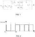
- FIG. 1 is a typical push-pull converter topology.
- An output voltage of a DC power source V DC supplies power to a load R by means of a transformer T 1 , a rectifier bridge formed by diodes D1-D4, and an inductor Li.
- a capacitor C 1 is connected in parallel to the load R.
- Two switching transistors S 1 and S 2 are turned on alternately. In a no-load state, respective duty cycles of the switching transistors S 1 and S 2 are very small. When a heavy load is suddenly applied, respective duty cycles of the switching transistors S 1 and S 2 increase rapidly. Referring to respective driving waveforms of the switching transistors S 1 and S 2 shown in FIG.
- the solid line and the dashed line respectively correspond to the driving waveform of S 1 and the driving waveform of S 2 .
- a heavy load is suddenly applied to the no-load converter. Because excitation of the transformer T 1 is very small before the time point t1, the excitation is ignored and considered to be approximately 0 herein.
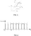
- An overly large duty cycle following the time point t1 forms an overly large unidirectional excitation change as shown in a curve 0 in FIG. 3 , and the overly large unidirectional excitation change is prone to cause the transformer T 1 to be magnetically saturated.
- a curve 1 in FIG. 3 is an excitation curve corresponding to normal operation.
- a conventional method is to increase respective switching frequencies of S 1 and S 2 .
- the driving waveforms are as shown in FIG. 4 , and the solid line and the dashed line respectively correspond to the driving waveform of S 1 and the driving waveform of S 2 .
- the switching period is shortened, on duration is also shorter than on duration in FIG. 2 , and therefore the transformer is prevented from being magnetically saturated.
- increasing the switching frequency significantly increases switching loss, and the increased switching loss further results in other problems such as a temperature rise.
- a control device for an isolated converter comprising:
- control device for the isolated converter according to the present invention, preferably, the control device further comprises a measurement module used to measure and output the load amount of the isolated converter.
- the switching frequency is directly increased to the first frequency value; when the load amount is greater than the second pre-configured threshold and is in the steady state, and if the switching frequency is greater than the second frequency value, then the switching frequency is gradually decreased to the second frequency value.
- the switching frequency is gradually decreased to the second frequency value at a specific step size, or is gradually decreased to the second frequency value according to a charging curve and a discharging curve of an RC circuit.
- control device for the isolated converter according to the present invention, preferably, the control device comprises a microcontroller, a time delay circuit, a transistor, a first resistor, a second resistor, a first capacitor, and a pulse width modulation chip, wherein
- the time delay circuit comprises a third resistor, a fourth resistor, a fifth resistor, a diode, and a second capacitor, a series branch formed by the third resistor and the fourth resistor is connected in parallel to a series branch formed by the diode and the fifth resistor, a node between the third resistor and the diode is connected to an output end of a digital signal module of the microcontroller, a node between the fourth resistor and the fifth resistor is connected to the base of the transistor, and a node between the third resistor and the fourth resistor is grounded via the second capacitor.
- the time delay circuit comprises an analog signal module, a software control unit, and a third resistor
- the analog signal module is connected to the output end of the microcontroller
- the software control unit is used to control an output analog signal of the analog signal module
- the analog signal end is connected to one end of the third resistor
- the other end of the third resistor is connected to the base of the transistor.
- the output end of the pulse width modulation chip is connected to the switching transistor of the isolated converter via a drive amplification circuit.
- the comparison module is comprised in the microcontroller.
- control device for the isolated converter according to the present invention
- the control device comprises an MCU connected to the switching transistor of the isolated converter, and the control device changes a period register value of a PWM generation module thereof on the basis of the comparison result of the load amount of the isolated converter and the pre-configured thresholds so as to change the switching frequency of the switching transistor.
- the present invention further provides a control method for an isolated converter, the control method comprising the following steps:
- the switching frequency is adjusted by monitoring and measuring the load amount, thereby solving the problem of temperature rising of the converter that occurs when the converter is fully loaded and operates stably, and effectively preventing the transformer from being magnetically saturated when a load is suddenly applied to the no-load converter.
- An embodiment of the present invention provides a switching frequency adjustment method for an isolated converter.
- the adjustment method adjusts a switching frequency according to a load so as to reduce switching loss.
- the adjustment method includes the following steps:
- a current switching frequency is less than the first frequency value. If the switching frequency is less than the first frequency value, then the switching frequency is increased to the first frequency value. If the switching frequency is not less than the first frequency value (is usually equal to the first frequency value), then the switching frequency is not adjusted, and load amount measurement continues. That is, if the load amount is not greater than the pre-configured threshold, then a high switching frequency (the first frequency value) is maintained to prevent a transformer of the isolated converter from being magnetically saturated. That is, magnetic induction intensity is maintained to be lower than or equal to maximum magnetic induction intensity at which the transformer is allowed to operate.
- the load amount is in the steady state. If the load amount is not steady, then load amount measurement continues. If the load amount is in the steady state, then it is further determined whether the current switching frequency is greater than the second frequency value (for example, 40 kHz). If the switching frequency is greater than the second frequency value, then the switching frequency is decreased to the second frequency value. If the switching frequency is not greater than the second frequency value (is usually equal to the second frequency value), then the switching frequency is not adjusted, and load amount measurement continues. That is, if the load amount is greater than the pre-configured threshold and is in the steady state, then a low switching frequency (the second frequency value) is maintained so that a temperature of the isolated converter does not exceed a maximum allowable temperature. The maximum temperature is a maximum temperature that components of the isolated converter can withstand.
- the second frequency value for example, 40 kHz
- the high first frequency value and the low second frequency value are selected according to a specific product model and an application scenario, and are preferably in the range of 1-500 kHz.
- a load switching hysteresis loop in order to prevent a system from repeatedly adjusting the switching frequency due to that an output load falls exactly at a load switching point (for example, 50% of a rated load), a load switching hysteresis loop can be added.
- a hysteresis loop width is configured to be 10% of the rated load.
- the high switching frequency is used.
- the switching frequency is gradually decreased to the low switching frequency.
- a pre-configured threshold range is configured on the basis of the aforementioned pre-configured threshold.
- the high switching frequency is used.
- the load amount is greater than a maximum value of the pre-configured threshold range, the low switching frequency is used.
- the load amount is exactly within the pre-configured threshold range, the original switching frequency remains unchanged, and the switching frequency is not adjusted.
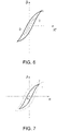
- a transformer excitation curve corresponding to increasing switching frequency shown in FIG. 6 changes in a transformer excitation curve corresponding to decreasing switching frequency shown in FIG. 7 .
- the switching frequency increases, the transformer excitation curve changes from a curve 1 to a curve 2 in FIG. 6 .
- the excitation curve shrinks, and the transformer is therefore not to be saturated. Therefore, the switching frequency can be increased rapidly. For example, the switching frequency jumps from a current frequency to the first frequency value (namely, changing from the current frequency directly to the first frequency value).
- the transformer excitation curve changes from a curve 1 to a curve 3 in FIG. 7 .
- the switching frequency is gradually decreased.
- the switching frequency is gradually decreased at a specific step size, so that the excitation curve changes smoothly, thereby preventing the transformer from being saturated.
- the specific step size may be a fixed value.
- the switching frequency is gradually decreased to the second frequency value at a step size of 1 kHz.
- the specific step size may also be a variable value.
- the switching frequency is gradually decreased to the second frequency value at a random step size of 1 kHz, 2 kHz, or 3 kHz.
- the second embodiment provides a switching frequency adjustment device for an isolated converter.
- the switching frequency adjustment device includes a measurement module 1, a comparison module 2, and an adjustment module 3.
- the measurement module 1 is used to measure a load amount and transmit a measurement result to the comparison module 2.
- the measurement module 1 may be a built-in measurement module in the isolated converter, and may also be a peripheral measurement module.
- a pre-configured threshold is prestored in the comparison module 2, and the comparison module 2 compares the received load amount with the pre-configured threshold, and transmits a comparison result to the adjustment module 3.
- the adjustment module 3 adjusts a switching frequency of a switching transistor S 1 or S 2 on the basis of the received comparison result, and meanwhile the switching frequency of the switch S 1 or S 2 can be fed back to the adjustment module 3.
- the switching frequency is increased to a first frequency value.
- the switching frequency is decreased to a second frequency value. Specifically, the adjustment module determines whether the load amount is greater than the pre-configured threshold.
- a current switching frequency is less than the first frequency value. If the switching frequency is less than the first frequency value, then the switching frequency is increased to the first frequency value. If the switching frequency is not less than the first frequency value (is usually equal to the first frequency value), then the switching frequency is not adjusted, and load amount measurement continues. That is, if the load amount is not greater than the pre-configured threshold, then a high switching frequency (the first frequency value) is maintained.
- the load amount is in the steady state. If the load amount is not steady, then load amount measurement continues. If the load amount is in the steady state, then it is further determined whether the current switching frequency is greater than the second frequency value (for example, 40 kHz). If so, then the switching frequency is decreased to the second frequency value. If the switching frequency is not greater than the second frequency value (is usually equal to the second frequency value), then the switching frequency is not adjusted, and load amount measurement continues. That is, if the load amount is greater than the pre-configured threshold and is in the steady state, then a low switching frequency (the second frequency value) is maintained.
- the second frequency value for example, 40 kHz
- a pre-configured threshold range is prestored in the comparison module 2.
- the high switching frequency is used.
- the load amount is greater than a maximum value of the pre-configured threshold range, the low switching frequency is used.
- the load amount is exactly within the pre-configured threshold range, the original switching frequency remains unchanged, and the switching frequency is not adjusted.
- the adjustment module 3 gradually decreases the switching frequency of the switching transistor S 1 or S 2 at a specific step size.
- a microcontroller MCU receives a comparison result of a load amount and a pre-configured threshold, and outputs a digital voltage signal by means of a digital interface IO on the basis of the comparison result.
- the digital voltage signal passes through a time delay circuit 20, controls a switching status (including an on state, an amplification state, and an off state) of a transistor Q1 to adjust external resistors R4 and R5 outside a pulse width modulation chip (PWM IC) oscillator so as to adjust an oscillation frequency of the PWM IC.
- the oscillation frequency corresponds to an output frequency of the PWM IC.
- the PWM IC is preferably connected to switching transistors S 1 and S 2 by means of a drive circuit so as to adjust a switching frequency thereof.
- the switching frequency is consistent with the output frequency of the PWM IC.
- the time delay circuit 20 includes resistors R1 and R2 connected in series to each other, a diode D1 and a resistor R3 connected in series to each other, and a capacitor C1.
- a branch formed by the resistors R1 and R2 is connected in parallel to a branch formed by the diode D1 and the resistor R3.
- a node between the resistor R1 and the diode D1 is connected to an IO interface of the MCU.
- Anode between the resistors R1 and R2 is grounded by means of the capacitor C1.
- a node between the resistors R2 and R3 is connected to a base of the transistor Q1.
- An emitter of the transistor Q1 is grounded.
- a collector of the transistor Q1 is connected to an RT pin of the PWM IC by means of a resistor R4.
- a CT pin of the PWM IC is grounded by means of a capacitor C6.
- a node between the resistor R4 and the RT pin is grounded by means of a resistor R5.
- the high level outputted by the MCU charges C1 by means of R1, and a voltage of C1 is gradually increased from a low level to a high level so as to prepare for changing of the MCU output from a high level to a low level.
- duration in which the output frequency of the PWM IC gradually changes from a high frequency to a low frequency depends on duration in which C1 discharges by means of R1. That is, the switching frequency is gradually decreased according to a charging curve and a discharging curve of an RC circuit, such as the example of a charging curve and a discharging curve of an RC circuit shown in FIG. 10 .
- a comparison module may be included in the microcontroller MCU.
- the comparison module receives load amount information, and compares the load amount with the pre-configured threshold.
- FIG. 11 Please refer to a schematic diagram of a circuit structure according to the second example of the switching frequency adjustment device of the present invention shown in FIG. 11 .
- Output of an MCU passes through an analog signal module (a DA module), and a variable analog voltage signal (DA output) is outputted.
- a DA module analog signal module
- DA output variable analog voltage signal
- drive capability is enhanced by means of a follower Op amp buffer, and then a switching status (including an on state, an amplification state, and an off state) of a transistor Q1 is controlled by means of a resistor R1 to adjust external resistors R4 and R5 outside a pulse width modulation chip (PWM IC) oscillator so as to adjust an oscillation frequency of the PWM IC.
- PWM IC pulse width modulation chip
- the oscillation frequency corresponds to an output frequency of the PWM IC.
- the PWM IC is preferably connected to switching transistors S 1 and S 2 by means of a drive circuit so as to adjust a switching frequency thereof.
- the switching frequency is consistent with the output frequency of the PWM IC.
- the analog signal module may be included in the MCU, and may also be arranged outside the MCU. Specifically, in this example, the analog signal module (the DA module), a software control unit for controlling an analog signal, the preferred follower, and the resistor R1 form a time delay circuit. A change speed of the output signal of the DA module is controlled by means of the software control unit so as to achieve rapid increase and gradual decrease of the output frequency of the PWM IC.
- a circuit following the resistor R1 is consistent with that in the first example. That is, an emitter of the transistor Q1 is grounded. A collector of the transistor Q1 is connected to an RT pin of the PWM IC by means of the resistor R4. A CT pin of the PWM IC is grounded by means of a capacitor C6. A node between the resistor R4 and the RT pin is grounded by means of the resistor R5.
- a speed at which the output frequency of the PWM IC gradually changes from a high frequency to a low frequency depends on a change speed of the DA signal controlled by the software unit.
- the time delay circuit according to the present invention is not limited to the circuit structures in the examples, and may have other variations as long as rapid increase and gradual decrease of the oscillation frequency of the PWM IC can be achieved.
- a digital control chip may also be used to implement switching frequency adjustment on S1 and S2 by means of software. For example, this can be readily implemented by changing a period register value of a PWM generation module in the MCU.
Landscapes
- Engineering & Computer Science (AREA)
- Power Engineering (AREA)
- Dc-Dc Converters (AREA)
Abstract
Description
- The present invention pertains to the field of power electronics, and in particular to a control method and control device for an isolated converter.
- A high-frequency transformer-based isolated converter is widely used in the field of power sources, especially in boost conversion of a battery voltage, and a push-pull DC-DC converter and a full-bridge DC-DC converter are most typical high-frequency transformer-based isolated converters.
-
FIG. 1 is a typical push-pull converter topology. An output voltage of a DC power source VDC supplies power to a load R by means of a transformer T1, a rectifier bridge formed by diodes D1-D4, and an inductor Li. A capacitor C1 is connected in parallel to the load R. Two switching transistors S1 and S2 are turned on alternately. In a no-load state, respective duty cycles of the switching transistors S1 and S2 are very small. When a heavy load is suddenly applied, respective duty cycles of the switching transistors S1 and S2 increase rapidly. Referring to respective driving waveforms of the switching transistors S1 and S2 shown inFIG. 2 , the solid line and the dashed line respectively correspond to the driving waveform of S1 and the driving waveform of S2. At a time point t1, a heavy load is suddenly applied to the no-load converter. Because excitation of the transformer T1 is very small before the time point t1, the excitation is ignored and considered to be approximately 0 herein. An overly large duty cycle following the time point t1 forms an overly large unidirectional excitation change as shown in acurve 0 inFIG. 3 , and the overly large unidirectional excitation change is prone to cause the transformer T1 to be magnetically saturated. Acurve 1 inFIG. 3 is an excitation curve corresponding to normal operation. - In order to solve this problem, a conventional method is to increase respective switching frequencies of S1 and S2. The driving waveforms are as shown in
FIG. 4 , and the solid line and the dashed line respectively correspond to the driving waveform of S1 and the driving waveform of S2. At the time point t1, a heavy load is suddenly applied to the no-load converter, and the duty cycle increases rapidly. However, because a switching period is shortened, on duration is also shorter than on duration inFIG. 2 , and therefore the transformer is prevented from being magnetically saturated. However, increasing the switching frequency significantly increases switching loss, and the increased switching loss further results in other problems such as a temperature rise. - In summary, for the high-frequency transformer-based isolated converter, when an output load is suddenly changed from no load to a full load, a driving pulse width of a switching transistor on a primary side of the transformer is suddenly changed from a very small duty cycle to a very large duty cycle. Because excitation of the transformer is very small in an initial stage, an overly large unidirectional excitation change is prone to cause magnetic induction intensity of the transformer to exceed a maximum value allowable for operation and therefore cause the transformer to be magnetically saturated. In order to prevent the transformer from being magnetically saturated, a conventional method is to increase a switching frequency of the switching transistor on the primary side of the transformer. However, this method significantly increases the switching loss, and increases heat dissipation costs of the converter.
- Therefore, the objective of the present invention is to eliminate the aforementioned defects of the prior art. A control device for an isolated converter is provided, the control device comprising:
- a comparison module, for receiving a load amount of the isolated converter, comparing the load amount with a first pre-configured threshold and a second pre-configured threshold, and outputting a comparison result; and
- an adjustment module, for receiving the comparison result and adjusting a switching frequency of a switching transistor of the isolated converter on the basis of the comparison result, wherein when the load amount is not greater than the first pre-configured threshold, the switching frequency is configured to be a first frequency value so as to prevent a transformer of the isolated converter from being magnetically saturated, and when the load amount is greater than the second pre-configured threshold and is in a steady state, the switching frequency is configured to be a second frequency value so that a temperature of the isolated converter does not exceed a maximum allowable temperature, wherein the first pre-configured threshold is less than or equal to the second pre-configured threshold, and the first frequency value is greater than the second frequency value.
- In the control device for the isolated converter according to the present invention, preferably, the control device further comprises a measurement module used to measure and output the load amount of the isolated converter.
- In the control device for the isolated converter according to the present invention, preferably, when the load amount is not greater than the first pre-configured threshold, and if the switching frequency is less than the first frequency value, then the switching frequency is directly increased to the first frequency value; when the load amount is greater than the second pre-configured threshold and is in the steady state, and if the switching frequency is greater than the second frequency value, then the switching frequency is gradually decreased to the second frequency value. Preferably, the switching frequency is gradually decreased to the second frequency value at a specific step size, or is gradually decreased to the second frequency value according to a charging curve and a discharging curve of an RC circuit.
- In the control device for the isolated converter according to the present invention, preferably, the control device comprises a microcontroller, a time delay circuit, a transistor, a first resistor, a second resistor, a first capacitor, and a pulse width modulation chip, wherein
- the microcontroller changes an output voltage thereof on the basis of the comparison result of the load amount of the isolated converter and the pre-configured thresholds;
- an output end of the microcontroller is connected to a base of the transistor via the time delay circuit, an emitter of the transistor is grounded, a collector of the transistor is connected to a first pin of the pulse width modulation chip via the first resistor, a node between the first pin and the first resistor is grounded via the second resistor, and a second pin of the pulse width modulation chip is grounded via the first capacitor;
- an output end of the pulse width modulation chip is connected to a switch of the isolated converter so as to adjust the switching frequency of the switching transistor,
- wherein the time delay circuit is used to achieve direct increase and gradual decrease of an output frequency of the pulse width modulation chip.
- In the control device for the isolated converter according to the present invention, preferably, the time delay circuit comprises a third resistor, a fourth resistor, a fifth resistor, a diode, and a second capacitor, a series branch formed by the third resistor and the fourth resistor is connected in parallel to a series branch formed by the diode and the fifth resistor, a node between the third resistor and the diode is connected to an output end of a digital signal module of the microcontroller, a node between the fourth resistor and the fifth resistor is connected to the base of the transistor, and a node between the third resistor and the fourth resistor is grounded via the second capacitor.
- In the control device for the isolated converter according to the present invention, preferably, the time delay circuit comprises an analog signal module, a software control unit, and a third resistor, the analog signal module is connected to the output end of the microcontroller, the software control unit is used to control an output analog signal of the analog signal module, the analog signal end is connected to one end of the third resistor, and the other end of the third resistor is connected to the base of the transistor.
- In the control device for the isolated converter according to the present invention, preferably, the output end of the pulse width modulation chip is connected to the switching transistor of the isolated converter via a drive amplification circuit.
- In the control device for the isolated converter according to the present invention, preferably, the comparison module is comprised in the microcontroller.
- In the control device for the isolated converter according to the present invention, preferably, the control device comprises an MCU connected to the switching transistor of the isolated converter, and the control device changes a period register value of a PWM generation module thereof on the basis of the comparison result of the load amount of the isolated converter and the pre-configured thresholds so as to change the switching frequency of the switching transistor.
- The present invention further provides a control method for an isolated converter, the control method comprising the following steps:
- a comparison step, for comparing a load amount of the isolated converter with a first pre-configured threshold and a second pre-configured threshold; and
- an adjustment step, for adjusting a switching frequency of a switching transistor of the isolated converter on the basis of a comparison result of the comparison step, wherein when the load amount is not greater than the first pre-configured threshold, the switching frequency is configured to be a first frequency value so as to prevent a transformer of the isolated converter from being magnetically saturated, and when the load amount is greater than the second pre-configured threshold and is in a steady state, the switching frequency is configured to be a second frequency value so that a temperature of the isolated converter does not exceed a maximum allowable temperature, wherein the first pre-configured threshold is less than or equal to the second pre-configured threshold, and the first frequency value is greater than the second frequency value.
- Compared with the prior art, in the present invention, the switching frequency is adjusted by monitoring and measuring the load amount, thereby solving the problem of temperature rising of the converter that occurs when the converter is fully loaded and operates stably, and effectively preventing the transformer from being magnetically saturated when a load is suddenly applied to the no-load converter.
- Embodiments of the present invention are further described below with reference to the accompanying drawings:
-
FIG. 1 is a typical push-pull converter topology; -
FIG. 2 shows respective driving waveforms of switching transistors S1 and S2 in the converter topology inFIG. 1 ; -
FIG. 3 shows an excitation curve of a transformer in the converter topology inFIG. 1 based on the driving waveforms shown inFIG. 2 ; -
FIG. 4 shows other respective driving waveforms of switching transistors S1 and S2 in the converter topology inFIG. 1 ; -
FIG. 5 shows a flowchart of a switching frequency adjustment method for an isolated converter according to a first embodiment of the present invention; -
FIG. 6 and FIG. 7 respectively show changes in a transformer excitation curve corresponding to increasing switching frequency and decreasing switching frequency; -
FIG. 8 shows a switching frequency adjustment device for an isolated converter according to a second embodiment of the present invention; -
FIG. 9 shows a schematic diagram of a circuit structure of a first example of a switching frequency adjustment device of the present invention; -
FIG. 10 shows an example of a charging curve and a discharging curve of an RC circuit; and -
FIG. 11 shows a schematic diagram of a circuit structure according to a second example of a switching frequency adjustment device of the present invention. - In order to make the objectives, technical solutions, and advantages of the present invention clearer, the present invention is further described in detail below via specific embodiments with reference to the accompanying drawings. It should be understood that the specific embodiments described herein are only intended to explain the present invention rather than to limit the present invention.
- An embodiment of the present invention provides a switching frequency adjustment method for an isolated converter. The adjustment method adjusts a switching frequency according to a load so as to reduce switching loss. For the specific adjustment method, please refer to the flowchart shown in
FIG. 5 . The adjustment method includes the following steps: -
step 1, start an isolated converter, and configure an initial switching frequency to be a first frequency value (for example, 55 kHz); -
step 2, measure a load amount, and compare the load amount with a pre-configured threshold (for example, 50% of rated power), where in the present invention, the load amount is preferably load power; and -
step 3, adjust the switching frequency of the isolated converter on the basis of a comparison result of the load amount and the pre-configured threshold, where when the load amount is not greater than the pre-configured threshold, the switching frequency is increased to the first frequency value, and when the load amount is greater than the pre-configured threshold and is in a steady state, the switching frequency is decreased to a second frequency value. In the present invention, the steady state refers to that the load amount remains at a constant value or remains substantially at a constant value (for example, fluctuating between 90% and 110% of the constant value) within a specific time period (for example, 2 s). However, this definition of the steady state is merely exemplary and is not limiting. - Specifically, it is determined whether the load amount is greater than the pre-configured threshold.
- If not, then it is further determined whether a current switching frequency is less than the first frequency value. If the switching frequency is less than the first frequency value, then the switching frequency is increased to the first frequency value. If the switching frequency is not less than the first frequency value (is usually equal to the first frequency value), then the switching frequency is not adjusted, and load amount measurement continues. That is, if the load amount is not greater than the pre-configured threshold, then a high switching frequency (the first frequency value) is maintained to prevent a transformer of the isolated converter from being magnetically saturated. That is, magnetic induction intensity is maintained to be lower than or equal to maximum magnetic induction intensity at which the transformer is allowed to operate.
- If so, then it is further determined whether the load amount is in the steady state. If the load amount is not steady, then load amount measurement continues. If the load amount is in the steady state, then it is further determined whether the current switching frequency is greater than the second frequency value (for example, 40 kHz). If the switching frequency is greater than the second frequency value, then the switching frequency is decreased to the second frequency value. If the switching frequency is not greater than the second frequency value (is usually equal to the second frequency value), then the switching frequency is not adjusted, and load amount measurement continues. That is, if the load amount is greater than the pre-configured threshold and is in the steady state, then a low switching frequency (the second frequency value) is maintained so that a temperature of the isolated converter does not exceed a maximum allowable temperature. The maximum temperature is a maximum temperature that components of the isolated converter can withstand.
- In the present invention, the high first frequency value and the low second frequency value are selected according to a specific product model and an application scenario, and are preferably in the range of 1-500 kHz.
- In this embodiment, in order to prevent a system from repeatedly adjusting the switching frequency due to that an output load falls exactly at a load switching point (for example, 50% of a rated load), a load switching hysteresis loop can be added. For example, a hysteresis loop width is configured to be 10% of the rated load.
- When the load amount is less than 45%, the high switching frequency is used.
- When the load amount is 45%-55%, the current switching frequency remains unchanged.
- When the load amount is greater than 55%, the switching frequency is gradually decreased to the low switching frequency.
- That is, a pre-configured threshold range is configured on the basis of the aforementioned pre-configured threshold. When the load amount is less than a minimum value of the pre-configured threshold range, the high switching frequency is used. When the load amount is greater than a maximum value of the pre-configured threshold range, the low switching frequency is used. When the load amount is exactly within the pre-configured threshold range, the original switching frequency remains unchanged, and the switching frequency is not adjusted.
- In addition, please refer to changes in a transformer excitation curve corresponding to increasing switching frequency shown in
FIG. 6 and changes in a transformer excitation curve corresponding to decreasing switching frequency shown inFIG. 7 . When the switching frequency increases, the transformer excitation curve changes from acurve 1 to acurve 2 inFIG. 6 . The excitation curve shrinks, and the transformer is therefore not to be saturated. Therefore, the switching frequency can be increased rapidly. For example, the switching frequency jumps from a current frequency to the first frequency value (namely, changing from the current frequency directly to the first frequency value). When the switching frequency decreases, the transformer excitation curve changes from acurve 1 to acurve 3 inFIG. 7 . Because the excitation curve expands, a sudden change in the frequency may cause the transformer to be saturated, and therefore, preferably, the switching frequency is gradually decreased. For example, the switching frequency is gradually decreased at a specific step size, so that the excitation curve changes smoothly, thereby preventing the transformer from being saturated. The specific step size may be a fixed value. For example, the switching frequency is gradually decreased to the second frequency value at a step size of 1 kHz. The specific step size may also be a variable value. For example, the switching frequency is gradually decreased to the second frequency value at a random step size of 1 kHz, 2 kHz, or 3 kHz. - The second embodiment provides a switching frequency adjustment device for an isolated converter. Referring to
FIG. 8 , the switching frequency adjustment device includes ameasurement module 1, acomparison module 2, and anadjustment module 3. Themeasurement module 1 is used to measure a load amount and transmit a measurement result to thecomparison module 2. Themeasurement module 1 may be a built-in measurement module in the isolated converter, and may also be a peripheral measurement module. A pre-configured threshold is prestored in thecomparison module 2, and thecomparison module 2 compares the received load amount with the pre-configured threshold, and transmits a comparison result to theadjustment module 3. Theadjustment module 3 adjusts a switching frequency of a switching transistor S1 or S2 on the basis of the received comparison result, and meanwhile the switching frequency of the switch S1 or S2 can be fed back to theadjustment module 3. When the load amount is not greater than the pre-configured threshold, the switching frequency is increased to a first frequency value. When the load amount is greater than the pre-configured threshold and is in a steady state, the switching frequency is decreased to a second frequency value. Specifically, the adjustment module determines whether the load amount is greater than the pre-configured threshold. - If not, then it is further determined whether a current switching frequency is less than the first frequency value. If the switching frequency is less than the first frequency value, then the switching frequency is increased to the first frequency value. If the switching frequency is not less than the first frequency value (is usually equal to the first frequency value), then the switching frequency is not adjusted, and load amount measurement continues. That is, if the load amount is not greater than the pre-configured threshold, then a high switching frequency (the first frequency value) is maintained.
- If so, then it is further determined whether the load amount is in the steady state. If the load amount is not steady, then load amount measurement continues. If the load amount is in the steady state, then it is further determined whether the current switching frequency is greater than the second frequency value (for example, 40 kHz). If so, then the switching frequency is decreased to the second frequency value. If the switching frequency is not greater than the second frequency value (is usually equal to the second frequency value), then the switching frequency is not adjusted, and load amount measurement continues. That is, if the load amount is greater than the pre-configured threshold and is in the steady state, then a low switching frequency (the second frequency value) is maintained.
- Preferably, a pre-configured threshold range is prestored in the
comparison module 2. When the load amount is less than a minimum value of the pre-configured threshold range, the high switching frequency is used. When the load amount is greater than a maximum value of the pre-configured threshold range, the low switching frequency is used. When the load amount is exactly within the pre-configured threshold range, the original switching frequency remains unchanged, and the switching frequency is not adjusted. - Preferably, the
adjustment module 3 gradually decreases the switching frequency of the switching transistor S1 or S2 at a specific step size. - Specific examples of the switching frequency adjustment device for the isolated converter are provided below.
- Please refer to a schematic diagram of a circuit structure of the first example of the switching frequency adjustment device of the present invention shown in
FIG. 9 . A microcontroller MCU receives a comparison result of a load amount and a pre-configured threshold, and outputs a digital voltage signal by means of a digital interface IO on the basis of the comparison result. The digital voltage signal passes through atime delay circuit 20, controls a switching status (including an on state, an amplification state, and an off state) of a transistor Q1 to adjust external resistors R4 and R5 outside a pulse width modulation chip (PWM IC) oscillator so as to adjust an oscillation frequency of the PWM IC. The oscillation frequency corresponds to an output frequency of the PWM IC. The PWM IC is preferably connected to switching transistors S1 and S2 by means of a drive circuit so as to adjust a switching frequency thereof. The switching frequency is consistent with the output frequency of the PWM IC. Specifically, thetime delay circuit 20 includes resistors R1 and R2 connected in series to each other, a diode D1 and a resistor R3 connected in series to each other, and a capacitor C1. A branch formed by the resistors R1 and R2 is connected in parallel to a branch formed by the diode D1 and the resistor R3. A node between the resistor R1 and the diode D1 is connected to an IO interface of the MCU. Anode between the resistors R1 and R2 is grounded by means of the capacitor C1. A node between the resistors R2 and R3 is connected to a base of the transistor Q1. An emitter of the transistor Q1 is grounded. A collector of the transistor Q1 is connected to an RT pin of the PWM IC by means of a resistor R4. A CT pin of the PWM IC is grounded by means of a capacitor C6. A node between the resistor R4 and the RT pin is grounded by means of a resistor R5. - A detailed control process of the switching frequency adjustment device of this example is as follows:
- (1) When an IO output signal of the MCU changes from a low level to a high level, D1 is turned on. A high-level voltage is provided to the base of Q1 by means of D1, and therefore Q1 is saturated and turned on. Connection between R4 and R5 is equivalent to parallel connection. In this case, because a resistance value of the RT pin of the PWM IC is small, the output frequency of the PWM IC is high.
- In addition, the high level outputted by the MCU charges C1 by means of R1, and a voltage of C1 is gradually increased from a low level to a high level so as to prepare for changing of the MCU output from a high level to a low level.
- (2) When the IO output signal of the MCU changes from the high level to the low level, the high-level C1 discharges by means of R1, and gradually changes from the high level to the low level. Q1 changes from a saturated on region to an amplification region and gradually to an off region. In this case, because the resistance value of the RT pin of the PWM IC is large and is equal to that of R5, the output frequency of the PWM IC is low.
- In this process, duration in which the output frequency of the PWM IC gradually changes from a high frequency to a low frequency depends on duration in which C1 discharges by means of R1. That is, the switching frequency is gradually decreased according to a charging curve and a discharging curve of an RC circuit, such as the example of a charging curve and a discharging curve of an RC circuit shown in
FIG. 10 . - It can be seen that in this example:
- 1) When the level of the digital voltage signal of the MCU changes, the output frequency of the PWM IC also changes synchronously.
- 2) By adjusting the time delay circuit, especially respective parameters of R1 and C1, a voltage change speed of C1 can be changed, and therefore an operation status of the transistor Q1 can be changed. If the collector (the C electrode) and the emitter (the E electrode) of the transistor are considered to be equivalent to a resistor, then a resistance value of the equivalent resistor changes with the voltage of C1. From the perspective of the PWM IC, a parallel resistance value of external oscillation resistors connected to the PWM IC changes with the voltage of C1, and this finally results in that the output frequency of the PWM IC changes with the voltage of C1. Therefore, by adjusting respective parameters of R1 and C1, the voltage change speed of C1 can be changed, and therefore a change speed of the output frequency of the PWM IC can be changed, thereby achieving rapid increase and gradual decrease of the output frequency of the PWM IC.
- 3) By adjusting a resistance value of R4, a resistance value of the external RT pin of the PWM IC can be changed, and therefore a change range of the output frequency of the PWM IC can be adjusted.
- Those skilled in the art can understand that in this example, a comparison module may be included in the microcontroller MCU. The comparison module receives load amount information, and compares the load amount with the pre-configured threshold.
- Please refer to a schematic diagram of a circuit structure according to the second example of the switching frequency adjustment device of the present invention shown in
FIG. 11 . On the basis of a comparison result of a load amount and a pre-configured threshold, Output of an MCU passes through an analog signal module (a DA module), and a variable analog voltage signal (DA output) is outputted. Preferably, drive capability is enhanced by means of a follower Op amp buffer, and then a switching status (including an on state, an amplification state, and an off state) of a transistor Q1 is controlled by means of a resistor R1 to adjust external resistors R4 and R5 outside a pulse width modulation chip (PWM IC) oscillator so as to adjust an oscillation frequency of the PWM IC. The oscillation frequency corresponds to an output frequency of the PWM IC. The PWM IC is preferably connected to switching transistors S1 and S2 by means of a drive circuit so as to adjust a switching frequency thereof. The switching frequency is consistent with the output frequency of the PWM IC. The analog signal module may be included in the MCU, and may also be arranged outside the MCU. Specifically, in this example, the analog signal module (the DA module), a software control unit for controlling an analog signal, the preferred follower, and the resistor R1 form a time delay circuit. A change speed of the output signal of the DA module is controlled by means of the software control unit so as to achieve rapid increase and gradual decrease of the output frequency of the PWM IC. In addition, in this example, a circuit following the resistor R1 is consistent with that in the first example. That is, an emitter of the transistor Q1 is grounded. A collector of the transistor Q1 is connected to an RT pin of the PWM IC by means of the resistor R4. A CT pin of the PWM IC is grounded by means of a capacitor C6. A node between the resistor R4 and the RT pin is grounded by means of the resistor R5. - A detailed control process of the switching frequency adjustment device of this example is as follows:
- (1) When a DA output signal of the MCU rapidly changes from a low level to a high level, Q1 is saturated and turned on. Connection between R4 and R5 is equivalent to parallel connection. In this case, because a resistance value of the RT pin of the PWM IC is small, the output frequency of the PWM IC is high.
- (2) When the DA output signal of the MCU gradually changes from the high level to the low level, Q1 changes from a saturated on region to an amplification region and gradually to an off region. In this case, because the resistance value of the RT pin of the PWM IC is large and is equal to that of R5, the output frequency of the PWM IC is low.
- In this process, a speed at which the output frequency of the PWM IC gradually changes from a high frequency to a low frequency depends on a change speed of the DA signal controlled by the software unit.
- It can be seen that in this example:
- 1) When the level of the DA output of the MCU changes, the output frequency of the PWM IC also changes synchronously.
- 2) By adjusting the time delay circuit, rapid increase and gradual decrease of the output frequency of the PWM IC can be achieved.
- 3) By adjusting a resistance value of R4, the resistance value of the external RT pin of the PWM IC can be changed, and therefore a change range of the output frequency of the PWM IC can be adjusted.
- The time delay circuit according to the present invention is not limited to the circuit structures in the examples, and may have other variations as long as rapid increase and gradual decrease of the oscillation frequency of the PWM IC can be achieved.
- In addition to implementing switching frequency adjustment by means of the hardware circuits in the aforementioned two examples, a digital control chip may also be used to implement switching frequency adjustment on S1 and S2 by means of software. For example, this can be readily implemented by changing a period register value of a PWM generation module in the MCU.
- 1) When the switching frequency needs to be rapidly increased, the period register value of the PWM generation module is directly changed to a target value.
- 2) When the switching frequency needs to be gradually decreased, a looping instruction is used to gradually change the period register value of the PWM generation module to the target value. By changing the target value of a period register, the change range of the switching frequency can be changed. By changing the number of times of looping and an amount of change in the period register value, the change speed of the switching frequency can be changed.
- In order to demonstrate the effect of the present invention, the inventor performed a test on Callisto HV RT 3kVA produced by Eaton. A method in the prior art was used. In order to prevent a transformer from being saturated, a switching frequency was configured to be 55 kHz. Discharging of a fully loaded battery resulted in a temperature rise. A temperature of a MOSFET rose over 140°C, but was still not steady. Therefore, the machine has to be turned off to end the test, and it was predicted that a highest temperature may reach 155°C. The solution of the present invention was used to perform a test again. The highest temperature of the MOSFET was lower than 110°C. Therefore, the problem of a temperature rise of a transformer is effectively solved.
- Although the present invention has been described through preferred embodiments, the present invention is not limited to the embodiments described herein, but includes various changes and variations made without departing from the scope of the present invention.
Claims (10)
- A control device for an isolated converter, the control device comprising:a comparison module, for receiving a load amount of the isolated converter, comparing the load amount with a first pre-configured threshold and a second pre-configured threshold, and outputting a comparison result; andan adjustment module, for receiving the comparison result and adjusting a switching frequency of a switching transistor of the isolated converter on the basis of the comparison result, wherein when the load amount is not greater than the first pre-configured threshold, the switching frequency is configured to be a first frequency value so as to prevent a transformer of the isolated converter from being magnetically saturated, and when the load amount is greater than the second pre-configured threshold and is in a steady state, the switching frequency is configured to be a second frequency value so that a temperature of the isolated converter does not exceed a maximum allowable temperature, wherein the first pre-configured threshold is less than or equal to the second pre-configured threshold, and the first frequency value is greater than the second frequency value.
- The control device for the isolated converter according to claim 1, the control device further comprising a measurement module used to measure and output the load amount of the isolated converter.
- The control device for the isolated converter according to claim 1, wherein when the load amount is not greater than the first pre-configured threshold, and if the switching frequency is less than the first frequency value, then the switching frequency is directly increased to the first frequency value; when the load amount is greater than the second pre-configured threshold and is in the steady state, and if the switching frequency is greater than the second frequency value, then the switching frequency is gradually decreased to the second frequency value.
- The control device for the isolated converter according to claim 3, the control device comprising a microcontroller, a time delay circuit, a transistor, a first resistor, a second resistor, a first capacitor, and a pulse width modulation chip, whereinthe microcontroller changes an output voltage thereof on the basis of the comparison result of the load amount of the isolated converter and the pre-configured thresholds;an output end of the microcontroller is connected to a base of the transistor via the time delay circuit, an emitter of the transistor is grounded, a collector of the transistor is connected to a first pin of the pulse width modulation chip via the first resistor, a node between the first pin and the first resistor is grounded via the second resistor, and a second pin of the pulse width modulation chip is grounded via the first capacitor;an output end of the pulse width modulation chip is connected to the switching transistor of the isolated converter so as to adjust the switching frequency of the switching transistor,wherein the time delay circuit is used to achieve direct increase and gradual decrease of an output frequency of the pulse width modulation chip.
- The control device for the isolated converter according to claim 4, wherein the time delay circuit comprises a third resistor, a fourth resistor, a fifth resistor, a diode, and a second capacitor, a series branch formed by the third resistor and the fourth resistor is connected in parallel to a series branch formed by the diode and the fifth resistor, a node between the third resistor and the diode is connected to an output end of a digital signal module of the microcontroller, a node between the fourth resistor and the fifth resistor is connected to the base of the transistor, and a node between the third resistor and the fourth resistor is grounded via the second capacitor.
- The control device for the isolated converter according to claim 4, wherein the time delay circuit comprises an analog signal module, a software control unit, and a third resistor, the analog signal module is connected to the output end of the microcontroller, the software control unit is used to control an output analog signal of the analog signal module, the analog signal end is connected to one end of the third resistor, and the other end of the third resistor is connected to the base of the transistor.
- The control device for the isolated converter according to any one of claims 4-6, wherein the output end of the pulse width modulation chip is connected to the switching transistor of the isolated converter via a drive amplification circuit.
- The control device for the isolated converter according to any one of claims 4-6, wherein the comparison module is comprised in the microcontroller.
- The control device for the isolated converter according to claim 3, the control device comprising a pulse width modulation chip connected to the switching transistor of the isolated converter, the pulse width modulation chip changing a period register value of a generation module thereof on the basis of the comparison result of the load amount of the isolated converter and the pre-configured thresholds so as to change the switching frequency of the switching transistor.
- A control method for an isolated converter, the control method comprising the following steps:a comparison step, for comparing a load amount of the isolated converter with a first pre-configured threshold and a second pre-configured threshold; andan adjustment step, for adjusting a switching frequency of a switching transistor of the isolated converter on the basis of a comparison result of the comparison step, wherein when the load amount is not greater than the first pre-configured threshold, the switching frequency is configured to be a first frequency value so as to prevent a transformer of the isolated converter from being magnetically saturated, and when the load amount is greater than the second pre-configured threshold and is in a steady state, the switching frequency is configured to be a second frequency value so that a temperature of the isolated converter does not exceed a maximum allowable temperature, wherein the first pre-configured threshold is less than or equal to the second pre-configured threshold, and the first frequency value is greater than the second frequency value.
Applications Claiming Priority (1)
| Application Number | Priority Date | Filing Date | Title |
|---|---|---|---|
| CN202110047186.6A CN114765422A (en) | 2021-01-14 | 2021-01-14 | Control method and control device for isolated converter |
Publications (2)
| Publication Number | Publication Date |
|---|---|
| EP4030607A1 true EP4030607A1 (en) | 2022-07-20 |
| EP4030607B1 EP4030607B1 (en) | 2025-10-29 |
Family
ID=80218571
Family Applications (1)
| Application Number | Title | Priority Date | Filing Date |
|---|---|---|---|
| EP22151626.3A Active EP4030607B1 (en) | 2021-01-14 | 2022-01-14 | Control method and control device of isolated converter |
Country Status (3)
| Country | Link |
|---|---|
| US (1) | US11863076B2 (en) |
| EP (1) | EP4030607B1 (en) |
| CN (1) | CN114765422A (en) |
Citations (5)
| Publication number | Priority date | Publication date | Assignee | Title |
|---|---|---|---|---|
| EP0250464A1 (en) * | 1985-12-17 | 1988-01-07 | Hughes Aircraft Co | Wide band, high efficiency simmer power supply for a laser flashlamp. |
| US20030090914A1 (en) * | 2001-11-09 | 2003-05-15 | Arian Jansen | Power converter |
| JP2004215417A (en) * | 2003-01-06 | 2004-07-29 | Fuji Electric Device Technology Co Ltd | DC / DC converter |
| JP2006246681A (en) * | 2005-03-07 | 2006-09-14 | Sharp Corp | Switching power supply |
| JP2014168355A (en) * | 2013-02-28 | 2014-09-11 | Fujitsu Telecom Networks Ltd | Forward converter of active clamp system and driving method thereof |
Family Cites Families (6)
| Publication number | Priority date | Publication date | Assignee | Title |
|---|---|---|---|---|
| US5657215A (en) * | 1995-08-29 | 1997-08-12 | Compaq Computer Corporation | Controlling switch-Mode power conversion |
| US6127816A (en) * | 1999-08-04 | 2000-10-03 | Hewlett-Packard Company | Multiple frequency switching power supply and methods to operate a switching power supply |
| CN103218007B (en) * | 2013-04-12 | 2015-04-08 | 刘昇澔 | Circuit system and control method for electronic converter |
| JP2019068592A (en) * | 2017-09-29 | 2019-04-25 | トヨタ自動車株式会社 | Electric power conversion device |
| JP6981212B2 (en) * | 2017-12-01 | 2021-12-15 | トヨタ自動車株式会社 | Contactless power transmission equipment and power transmission system |
| JP6993905B2 (en) * | 2018-03-06 | 2022-01-14 | 株式会社Soken | DC / DC converter control device |
-
2021
- 2021-01-14 CN CN202110047186.6A patent/CN114765422A/en active Pending
-
2022
- 2022-01-12 US US17/574,125 patent/US11863076B2/en active Active
- 2022-01-14 EP EP22151626.3A patent/EP4030607B1/en active Active
Patent Citations (5)
| Publication number | Priority date | Publication date | Assignee | Title |
|---|---|---|---|---|
| EP0250464A1 (en) * | 1985-12-17 | 1988-01-07 | Hughes Aircraft Co | Wide band, high efficiency simmer power supply for a laser flashlamp. |
| US20030090914A1 (en) * | 2001-11-09 | 2003-05-15 | Arian Jansen | Power converter |
| JP2004215417A (en) * | 2003-01-06 | 2004-07-29 | Fuji Electric Device Technology Co Ltd | DC / DC converter |
| JP2006246681A (en) * | 2005-03-07 | 2006-09-14 | Sharp Corp | Switching power supply |
| JP2014168355A (en) * | 2013-02-28 | 2014-09-11 | Fujitsu Telecom Networks Ltd | Forward converter of active clamp system and driving method thereof |
Non-Patent Citations (1)
| Title |
|---|
| PANOV Y ET AL: "PERFORMANCE EVALUATION OF 70-W TWO-STAGE ADAPTERS FOR NOTEBOOK COMPUTERS", APEC '99. 14TH ANNUAL APPLIED POWER ELECTRONICS CONFERENCE AND EXPOSITION. DALLAS,TX, MARCH 14 - 18, 1999; [ANNUAL APPLIED POWER ELECTRONICS CONFERENCE], NEW YORK, NY : IEEE, US, vol. 2, 14 March 1999 (1999-03-14), pages 1059 - 1065, XP001004134, ISBN: 978-0-7803-5161-5 * |
Also Published As
| Publication number | Publication date |
|---|---|
| US11863076B2 (en) | 2024-01-02 |
| EP4030607B1 (en) | 2025-10-29 |
| CN114765422A (en) | 2022-07-19 |
| US20220224235A1 (en) | 2022-07-14 |
Similar Documents
| Publication | Publication Date | Title |
|---|---|---|
| US7492615B2 (en) | Switching power supply | |
| KR100889528B1 (en) | Soft-Start Circuit and Power Supply Containing It | |
| US8575854B2 (en) | Power conversion apparatus, discharge lamp ballast and headlight ballast | |
| US9966849B1 (en) | Current mode voltage converter having fast transient response | |
| TWI385494B (en) | Soft start circuit, power supply controller, and method therefor | |
| US11742763B2 (en) | Switching control circuit and power supply circuit | |
| JP3839737B2 (en) | DC voltage conversion circuit | |
| US12170482B2 (en) | Control circuit for switching converter with minimum on-time and off-time control and wide duty range | |
| US12027974B2 (en) | Control circuit and switching converter | |
| US20230261575A1 (en) | Buck converter circuit with seamless pwm/pfm transition | |
| US20080252276A1 (en) | Method of Forming a Buck-Boost Mode Power Supply Controller and Structure Therefor | |
| CN108702086B (en) | DC/DC Resonant Converter and Power Factor Correction Using Resonant Converter and Corresponding Control Method | |
| CN100375378C (en) | Control device, switching mode power converter and method for reducing audible noise | |
| CN114696613A (en) | Oscillator of switch converter and switch converter | |
| CN104753330A (en) | Soft start method of power management | |
| TW201923504A (en) | Switching regulator | |
| EP4030607B1 (en) | Control method and control device of isolated converter | |
| JP6714519B2 (en) | Switching power supply | |
| EP4340203B1 (en) | Control device for a switching voltage regulator having reduced audio noise and control method | |
| US11705909B1 (en) | Frequency-locked circuit for variable frequency topology and frequency-locked method thereof | |
| US20200228009A1 (en) | Power converter with multi-mode timing control | |
| US11929671B2 (en) | Current-mode control for multistage interleaved resonant converters | |
| KR101022613B1 (en) | Integrated circuits for AC power supplies and AC power supplies | |
| CN114400896A (en) | Integrated circuit and power supply device | |
| JP3490049B2 (en) | Switching power supply |
Legal Events
| Date | Code | Title | Description |
|---|---|---|---|
| PUAI | Public reference made under article 153(3) epc to a published international application that has entered the european phase |
Free format text: ORIGINAL CODE: 0009012 |
|
| STAA | Information on the status of an ep patent application or granted ep patent |
Free format text: STATUS: THE APPLICATION HAS BEEN PUBLISHED |
|
| AK | Designated contracting states |
Kind code of ref document: A1 Designated state(s): AL AT BE BG CH CY CZ DE DK EE ES FI FR GB GR HR HU IE IS IT LI LT LU LV MC MK MT NL NO PL PT RO RS SE SI SK SM TR |
|
| STAA | Information on the status of an ep patent application or granted ep patent |
Free format text: STATUS: REQUEST FOR EXAMINATION WAS MADE |
|
| 17P | Request for examination filed |
Effective date: 20230117 |
|
| RBV | Designated contracting states (corrected) |
Designated state(s): AL AT BE BG CH CY CZ DE DK EE ES FI FR GB GR HR HU IE IS IT LI LT LU LV MC MK MT NL NO PL PT RO RS SE SI SK SM TR |
|
| P01 | Opt-out of the competence of the unified patent court (upc) registered |
Effective date: 20230521 |
|
| STAA | Information on the status of an ep patent application or granted ep patent |
Free format text: STATUS: EXAMINATION IS IN PROGRESS |
|
| 17Q | First examination report despatched |
Effective date: 20231127 |
|
| GRAP | Despatch of communication of intention to grant a patent |
Free format text: ORIGINAL CODE: EPIDOSNIGR1 |
|
| STAA | Information on the status of an ep patent application or granted ep patent |
Free format text: STATUS: GRANT OF PATENT IS INTENDED |
|
| INTG | Intention to grant announced |
Effective date: 20250424 |
|
| GRAJ | Information related to disapproval of communication of intention to grant by the applicant or resumption of examination proceedings by the epo deleted |
Free format text: ORIGINAL CODE: EPIDOSDIGR1 |
|
| STAA | Information on the status of an ep patent application or granted ep patent |
Free format text: STATUS: EXAMINATION IS IN PROGRESS |
|
| INTC | Intention to grant announced (deleted) | ||
| GRAS | Grant fee paid |
Free format text: ORIGINAL CODE: EPIDOSNIGR3 |
|
| STAA | Information on the status of an ep patent application or granted ep patent |
Free format text: STATUS: GRANT OF PATENT IS INTENDED |
|
| GRAP | Despatch of communication of intention to grant a patent |
Free format text: ORIGINAL CODE: EPIDOSNIGR1 |
|
| INTG | Intention to grant announced |
Effective date: 20250818 |
|
| GRAA | (expected) grant |
Free format text: ORIGINAL CODE: 0009210 |
|
| STAA | Information on the status of an ep patent application or granted ep patent |
Free format text: STATUS: THE PATENT HAS BEEN GRANTED |
|
| AK | Designated contracting states |
Kind code of ref document: B1 Designated state(s): AL AT BE BG CH CY CZ DE DK EE ES FI FR GB GR HR HU IE IS IT LI LT LU LV MC MK MT NL NO PL PT RO RS SE SI SK SM TR |
|
| REG | Reference to a national code |
Ref country code: CH Ref legal event code: F10 Free format text: ST27 STATUS EVENT CODE: U-0-0-F10-F00 (AS PROVIDED BY THE NATIONAL OFFICE) Effective date: 20251029 Ref country code: GB Ref legal event code: FG4D |
|
| REG | Reference to a national code |
Ref country code: IE Ref legal event code: FG4D |
|
| REG | Reference to a national code |
Ref country code: DE Ref legal event code: R096 Ref document number: 602022023715 Country of ref document: DE |
|
| PGFP | Annual fee paid to national office [announced via postgrant information from national office to epo] |
Ref country code: GB Payment date: 20251219 Year of fee payment: 5 |
|
| PGFP | Annual fee paid to national office [announced via postgrant information from national office to epo] |
Ref country code: FR Payment date: 20251217 Year of fee payment: 5 |
|
| REG | Reference to a national code |
Ref country code: NL Ref legal event code: MP Effective date: 20251029 |
|
| PG25 | Lapsed in a contracting state [announced via postgrant information from national office to epo] |
Ref country code: ES Free format text: LAPSE BECAUSE OF FAILURE TO SUBMIT A TRANSLATION OF THE DESCRIPTION OR TO PAY THE FEE WITHIN THE PRESCRIBED TIME-LIMIT Effective date: 20251029 |
|
| REG | Reference to a national code |
Ref country code: LT Ref legal event code: MG9D |
|
| PG25 | Lapsed in a contracting state [announced via postgrant information from national office to epo] |
Ref country code: NO Free format text: LAPSE BECAUSE OF FAILURE TO SUBMIT A TRANSLATION OF THE DESCRIPTION OR TO PAY THE FEE WITHIN THE PRESCRIBED TIME-LIMIT Effective date: 20260129 |
|
| PGFP | Annual fee paid to national office [announced via postgrant information from national office to epo] |
Ref country code: DE Payment date: 20251217 Year of fee payment: 5 |
|
| PG25 | Lapsed in a contracting state [announced via postgrant information from national office to epo] |
Ref country code: FI Free format text: LAPSE BECAUSE OF FAILURE TO SUBMIT A TRANSLATION OF THE DESCRIPTION OR TO PAY THE FEE WITHIN THE PRESCRIBED TIME-LIMIT Effective date: 20251029 Ref country code: AT Free format text: LAPSE BECAUSE OF FAILURE TO SUBMIT A TRANSLATION OF THE DESCRIPTION OR TO PAY THE FEE WITHIN THE PRESCRIBED TIME-LIMIT Effective date: 20251029 Ref country code: HR Free format text: LAPSE BECAUSE OF FAILURE TO SUBMIT A TRANSLATION OF THE DESCRIPTION OR TO PAY THE FEE WITHIN THE PRESCRIBED TIME-LIMIT Effective date: 20251029 |
|
| PGFP | Annual fee paid to national office [announced via postgrant information from national office to epo] |
Ref country code: AT Payment date: 20260301 Year of fee payment: 5 |
|
| REG | Reference to a national code |
Ref country code: AT Ref legal event code: MK05 Ref document number: 1852821 Country of ref document: AT Kind code of ref document: T Effective date: 20251029 |
|
| PG25 | Lapsed in a contracting state [announced via postgrant information from national office to epo] |
Ref country code: NL Free format text: LAPSE BECAUSE OF FAILURE TO SUBMIT A TRANSLATION OF THE DESCRIPTION OR TO PAY THE FEE WITHIN THE PRESCRIBED TIME-LIMIT Effective date: 20251029 |
|
| PG25 | Lapsed in a contracting state [announced via postgrant information from national office to epo] |
Ref country code: RS Free format text: LAPSE BECAUSE OF FAILURE TO SUBMIT A TRANSLATION OF THE DESCRIPTION OR TO PAY THE FEE WITHIN THE PRESCRIBED TIME-LIMIT Effective date: 20260129 |
|
| PG25 | Lapsed in a contracting state [announced via postgrant information from national office to epo] |
Ref country code: IS Free format text: LAPSE BECAUSE OF FAILURE TO SUBMIT A TRANSLATION OF THE DESCRIPTION OR TO PAY THE FEE WITHIN THE PRESCRIBED TIME-LIMIT Effective date: 20260228 |
|
| PG25 | Lapsed in a contracting state [announced via postgrant information from national office to epo] |
Ref country code: PT Free format text: LAPSE BECAUSE OF FAILURE TO SUBMIT A TRANSLATION OF THE DESCRIPTION OR TO PAY THE FEE WITHIN THE PRESCRIBED TIME-LIMIT Effective date: 20260302 |
|
| PG25 | Lapsed in a contracting state [announced via postgrant information from national office to epo] |
Ref country code: PL Free format text: LAPSE BECAUSE OF FAILURE TO SUBMIT A TRANSLATION OF THE DESCRIPTION OR TO PAY THE FEE WITHIN THE PRESCRIBED TIME-LIMIT Effective date: 20251029 |
|
| PG25 | Lapsed in a contracting state [announced via postgrant information from national office to epo] |
Ref country code: LV Free format text: LAPSE BECAUSE OF FAILURE TO SUBMIT A TRANSLATION OF THE DESCRIPTION OR TO PAY THE FEE WITHIN THE PRESCRIBED TIME-LIMIT Effective date: 20251029 |
|
| PG25 | Lapsed in a contracting state [announced via postgrant information from national office to epo] |
Ref country code: BG Free format text: LAPSE BECAUSE OF FAILURE TO SUBMIT A TRANSLATION OF THE DESCRIPTION OR TO PAY THE FEE WITHIN THE PRESCRIBED TIME-LIMIT Effective date: 20251029 |