EP4028894B1 - Sdio-chip-zu-chip-verbindungsprotokollerweiterung für langsame geräte und leistungseinsparung - Google Patents
Sdio-chip-zu-chip-verbindungsprotokollerweiterung für langsame geräte und leistungseinsparung Download PDFInfo
- Publication number
- EP4028894B1 EP4028894B1 EP20754116.0A EP20754116A EP4028894B1 EP 4028894 B1 EP4028894 B1 EP 4028894B1 EP 20754116 A EP20754116 A EP 20754116A EP 4028894 B1 EP4028894 B1 EP 4028894B1
- Authority
- EP
- European Patent Office
- Prior art keywords
- host
- client device
- client
- data
- event register
- Prior art date
- Legal status (The legal status is an assumption and is not a legal conclusion. Google has not performed a legal analysis and makes no representation as to the accuracy of the status listed.)
- Active
Links
Images






Classifications
-
- G—PHYSICS
- G06—COMPUTING OR CALCULATING; COUNTING
- G06F—ELECTRIC DIGITAL DATA PROCESSING
- G06F9/00—Arrangements for program control, e.g. control units
- G06F9/06—Arrangements for program control, e.g. control units using stored programs, i.e. using an internal store of processing equipment to receive or retain programs
- G06F9/46—Multiprogramming arrangements
- G06F9/54—Interprogram communication
- G06F9/542—Event management; Broadcasting; Multicasting; Notifications
-
- G—PHYSICS
- G06—COMPUTING OR CALCULATING; COUNTING
- G06F—ELECTRIC DIGITAL DATA PROCESSING
- G06F13/00—Interconnection of, or transfer of information or other signals between, memories, input/output devices or central processing units
- G06F13/38—Information transfer, e.g. on bus
- G06F13/42—Bus transfer protocol, e.g. handshake; Synchronisation
- G06F13/4282—Bus transfer protocol, e.g. handshake; Synchronisation on a serial bus, e.g. I2C bus, SPI bus
- G06F13/4291—Bus transfer protocol, e.g. handshake; Synchronisation on a serial bus, e.g. I2C bus, SPI bus using a clocked protocol
-
- G—PHYSICS
- G06—COMPUTING OR CALCULATING; COUNTING
- G06F—ELECTRIC DIGITAL DATA PROCESSING
- G06F13/00—Interconnection of, or transfer of information or other signals between, memories, input/output devices or central processing units
- G06F13/38—Information transfer, e.g. on bus
- G06F13/40—Bus structure
- G06F13/4063—Device-to-bus coupling
-
- G—PHYSICS
- G06—COMPUTING OR CALCULATING; COUNTING
- G06F—ELECTRIC DIGITAL DATA PROCESSING
- G06F13/00—Interconnection of, or transfer of information or other signals between, memories, input/output devices or central processing units
- G06F13/38—Information transfer, e.g. on bus
- G06F13/42—Bus transfer protocol, e.g. handshake; Synchronisation
- G06F13/4204—Bus transfer protocol, e.g. handshake; Synchronisation on a parallel bus
- G06F13/4208—Bus transfer protocol, e.g. handshake; Synchronisation on a parallel bus being a system bus, e.g. VME bus, Futurebus, Multibus
- G06F13/4217—Bus transfer protocol, e.g. handshake; Synchronisation on a parallel bus being a system bus, e.g. VME bus, Futurebus, Multibus with synchronous protocol
-
- G—PHYSICS
- G06—COMPUTING OR CALCULATING; COUNTING
- G06F—ELECTRIC DIGITAL DATA PROCESSING
- G06F9/00—Arrangements for program control, e.g. control units
- G06F9/06—Arrangements for program control, e.g. control units using stored programs, i.e. using an internal store of processing equipment to receive or retain programs
- G06F9/30—Arrangements for executing machine instructions, e.g. instruction decode
- G06F9/30098—Register arrangements
-
- G—PHYSICS
- G06—COMPUTING OR CALCULATING; COUNTING
- G06F—ELECTRIC DIGITAL DATA PROCESSING
- G06F9/00—Arrangements for program control, e.g. control units
- G06F9/06—Arrangements for program control, e.g. control units using stored programs, i.e. using an internal store of processing equipment to receive or retain programs
- G06F9/46—Multiprogramming arrangements
- G06F9/466—Transaction processing
-
- G—PHYSICS
- G06—COMPUTING OR CALCULATING; COUNTING
- G06F—ELECTRIC DIGITAL DATA PROCESSING
- G06F9/00—Arrangements for program control, e.g. control units
- G06F9/06—Arrangements for program control, e.g. control units using stored programs, i.e. using an internal store of processing equipment to receive or retain programs
- G06F9/46—Multiprogramming arrangements
- G06F9/54—Interprogram communication
- G06F9/544—Buffers; Shared memory; Pipes
-
- Y—GENERAL TAGGING OF NEW TECHNOLOGICAL DEVELOPMENTS; GENERAL TAGGING OF CROSS-SECTIONAL TECHNOLOGIES SPANNING OVER SEVERAL SECTIONS OF THE IPC; TECHNICAL SUBJECTS COVERED BY FORMER USPC CROSS-REFERENCE ART COLLECTIONS [XRACs] AND DIGESTS
- Y02—TECHNOLOGIES OR APPLICATIONS FOR MITIGATION OR ADAPTATION AGAINST CLIMATE CHANGE
- Y02D—CLIMATE CHANGE MITIGATION TECHNOLOGIES IN INFORMATION AND COMMUNICATION TECHNOLOGIES [ICT], I.E. INFORMATION AND COMMUNICATION TECHNOLOGIES AIMING AT THE REDUCTION OF THEIR OWN ENERGY USE
- Y02D10/00—Energy efficient computing, e.g. low power processors, power management or thermal management
Definitions
- the present disclosure generally relates to apparatuses incorporating integrated circuits (ICs). More specifically, aspects of the present disclosure relate to a secure digital (SD) input/output (SDIO) chip-to-chip interconnect protocol extension for slow devices and power savings.
- SD secure digital
- SDIO secure digital input/output
- Communications links use different methods for controlling the flow of commands and data between interconnected devices. For example, one device may operate as a master of a communications link, while other devices operate as slaves on the communications link. In this master/slave configuration, the master device issues commands on the communications link that permit the slave devices to communicate. If a particular slave device does not receive an appropriate command, then the device does not transmit on the communications link. A single master device, therefore, controls the flow of commands and data on the communications link.
- SDIO secure digital input/output
- An SDIO system is useful for two-way communications with the client devices in a computer system.
- the SDIO protocol relies on an SDIO host to communicate with client devices within a personal computer (PC) or other mobile computing device.
- the SDIO host operates as an SDIO master and controls other SDIO slave devices connected to the SDIO host. Data flow is controlled and monitored by the SDIO host.
- the SDIO protocol is entirely host/master driven. Slave devices operating according to the SDIO protocol cannot initiate data transfers.
- a system for permitting communication between an SD client device and an SD host to trigger the SD host to issue an SD direct command to the SD client device is desired.
- US 2012/260008 A1 discloses a non-transitory, tangible computer readable storage medium encoded with processor readable instructions to perform a method of transferring SDIO data.
- One method comprises buffering multiple IP packets to transfer from one of a SDCC host and a SDIO client to the other of the SDCC host and the SDIO client.
- a multiplexing header is attached to each of the multiple IP packets and one of at least one SDIO read command and at least one SDIO write command issued.
- the multiple IP packets are then transferred in a single SDIO transfer between the one of a SDCC host and a SDIO client to the other of the SDCC host and the SDIO client.
- SDIO secure digital input/output
- An SDIO system is useful for host initiated two-way communications with the client devices in a computer system.
- the SDIO protocol relies on an SDIO host to communicate with client devices within a personal computer (PC) or other mobile computing device.
- the SDIO host operates as an SDIO master and controls other SDIO slave devices connected to the SDIO host. Data flow is controlled and monitored by the SDIO host.
- the SDIO protocol is entirely host/master driven. Slave devices operating according to the SDIO protocol cannot initiate data transfers on an SD bus communicably coupling the slave devices and the host/master. This inability to initiate data communications from the slave devices may violate latency specifications of the SDIO protocol, resulting in timeout errors of SDIO transactions. It is, therefore, desirable to provide a system for permitting communication between an SD client device and an SD host to trigger the SD host to issue an SD direct command to the SD target device.
- a system permits communication between an SD client device and an SD host for triggering the issuing of an SD direct command from the SD host to the SD client device. Triggering of an SD direct command is enabled by a client event register (CER) within the register space of the target device and the address space of the SD host.
- CER client event register
- HER host event register
- the host event register and client event register may prevent timeout of low speed embedded (e.g., Internet-of-things (IOT)) devices when operating in a low power mode (LPM) in response to an SD direct command from an SD host. Preventing timeout of low speed embedded devices may improve boot-loader hardware to expedite device boot-up.
- low speed embedded e.g., Internet-of-things (IOT)
- LPM low power mode
- FIGURE 1 is a block diagram illustrating an example implementation of a host system-on-a-chip (SOC) 100, which includes a connectivity block 110 configured to trigger secure digital (SD) direct commands over an SD bus, in accordance with aspects of the present disclosure.
- the host SOC 100 includes processing blocks tailored to specific functions, such as a connectivity block 110.
- the connectivity block 110 may include fifth generation (5G) connectivity, fourth generation long term evolution (4G LTE) connectivity, Wi-Fi connectivity, USB connectivity, Bluetooth connectivity, Secure Digital (SD) connectivity, and the like.
- 5G fifth generation
- 4G LTE fourth generation long term evolution
- Wi-Fi connectivity Wireless Fidelity
- USB connectivity Wireless Fidelity
- Bluetooth connectivity Secure Digital
- the host SOC 100 includes various processing units that support multi-threaded operation.
- the host SOC 100 includes a multi-core central processing unit (CPU) 102, a graphics processor unit (GPU) 104, a digital signal processor (DSP) 106, and a neural processor unit (NPU) 108.
- the host SOC 100 may also include a sensor processor 114, image signal processors (ISPs) 116, a navigation module 120, which may include a global positioning system, and a memory 118.
- the multi-core CPU 102, the GPU 104, the DSP 106, the NPU 108, and the multi-media engine 112 support various functions such as video, audio, graphics, gaming, artificial networks, and the like.
- Each processor core of the multi-core CPU 102 may be a reduced instruction set computing (RISC) machine, an advance RISC machine (ARM), a microprocessor, or some other type of processor.
- the NPU 108 may be based on an ARM instruction set.
- FIGURE 2 is a block diagram illustrating an example implementation of signal pins for a secure digital (SD) host communicably coupled to SD slave devices in a host/slave SD input/output (SDIO) configuration, in accordance with aspects of the present disclosure.
- a host/master 200 may be the host SOC 100, or a block of the host SOC 100, such as the connectivity block 110 or other like block of the host SOC 100, including a secure digital (SD) controller/interface 210.
- the host/master 200 includes the SD controller/interface 210, configured to communicate with client/slave devices 230 (230-1, ... , 230-N) over an SD bus 220.
- the SD bus 220 is configured according to the SDIO protocol and carries a clock (CLK) signal, an SD command (CMD) signal, and a data signal (DAT[3:0]).
- CLK clock
- CMD SD command
- DAT[3:0] data signal
- the SDIO protocol is entirely driven by the host/master 200.
- the client/slave devices 230 cannot initiate any data transfers.
- the host/master 200 uses SD commands for controlling data transfers as well as communications to/from the client/slave devices 230.
- the host/master 200 uses an SD direct command (e.g., command fifty-two (CMD52)) for performing byte reads and issuing abort commands.
- CMD52 command fifty-two
- the host/master 200 uses an SD extended command (e.g., command fifty-three (CMD53)) for performing burst reads and writes from/to the client/slave devices 230. That is, an SD extended command may be a CMD53 read command or a CMD53 write command.
- SD extended command e.g., command fifty-three (CMD53)
- CMD53 command fifty-three
- the host/master 200 is generally configured to perform burst data transfers using the CMD53 command for performing both read and write operations.
- a command header is communicated from the host/master 200 to one of the client/slave devices 230 prior to data transfer.
- the command header generally indicates a packet data size and is immediately followed by the packet data.
- a dataflow from the host/master 200 to the client/slave devices 230 may be referred to as a transmit direction.
- a dataflow from the client/slave devices 230 to the host/master 200 may be referred to as a receive direction.
- a state of the client/slave devices 230 may introduce unwanted latency, resulting in a timeout error of a data transaction over the SD bus 220.
- FIGURE 3 is a timing diagram further illustrating the host/slave SDIO configuration of FIGURE 2 during a normal data transfer, in accordance with aspects of the present disclosure.
- the SDIO protocol is based on a master/slave configuration specified by the SD Card Association.
- an SD host 300 controls reading/writing of data from an SD client device 330 by issuing CMD52/CMD53 SDIO direct commands to read/write from/to the SD client device 330.
- the SD client device 330 when active, responds to these SD direct commands.
- the SD host 300 issues a CMD53 data write request to the SD client device 330, at time 310.
- the SDIO protocol enables the SD host 300 to specify a time period (T) in which the SD client device 330 creates a client buffer to complete the CMD53 data write request.
- T time period
- the SD client device 330 is likely an I/O device (e.g., a mobile station modem (MSM))
- MSM mobile station modem
- a data processing speed depends on the actual I/O operation performed by the SD client device 330.
- the processing speed also depends on each I/O function performed by the SD client device 330 and the amount of data prepared may depend on the application and the capability of the SD client device 330.
- the SD client device 330 responds to the SD host 300 by issuing a data response to complete the write operation, at time 312.
- FIGURE 4 is a timing diagram further illustrating the host/slave SDIO configuration of FIGURE 3 during timeout of a data transfer due to a low speed target device, in accordance with aspects of the present disclosure.
- the SD host 300 issues a CMD53 write data request to the SD client device 330, at time 410.
- the write transaction from the SD host 300 times out due to expiration of a transaction timeout T of the SD host 300.
- the timeout occurs because the SD client device 330 responds to the CMD53 write request after a time period (T + t) by issuing the CMD53 data response to the SD host 300, at time 412.
- FIGURE 4 illustrates a data preparation delay period (t) that causes a timeout of the write transaction from the SD host 300.
- This data preparation delay period (t) may be due to the configuration of the SD client device 330.
- timeout of the host write transaction may occur when the SD client device 330 is configured as a low speed embedded (e.g., Internet-of-things (IOT)) device.
- IOT Internet-of-things
- the operating speed of the SD client device 330 leads to a data preparation timeout in response to the CMD53 write data request.
- the data preparation may involve allocation of buffer space of the SD client device 330 to accommodate incoming packet data from the SD host 300.
- FIGURE 5 is a timing diagram further illustrating the host/slave SDIO configuration of FIGURE 3 during timeout of a data transfer due to a low power mode (LPM)/sleep mode target device, in accordance with aspects of the present disclosure.
- LPM low power mode
- synchronization between the SD host 300 and the SD client device 330 may be lost when the SD client device 330 operates in a LPM/sleep mode.
- relatively slow devices e.g. IOT devices
- low speed embedded devices may exceed the timeout period (T) specified by the SD host 300 for the data write transaction.
- the SD client device 330 operates in an LPM/sleep mode when the SD host 300 issues the CMD53 write data request, at time 510.
- the CMD53 write data request interrupts operation of the SD target device.
- the SD client device 330 is delayed for a time period (t) to come out of the LPM/sleep mode and then sends a response at time 512, after a time period (T+t). It is likely the full cycle for the host transaction will not be completed within the timeout period T specified by the SD host 300. In this example, the host transaction times out because the CMD53 data response from the SD client device 330 is transmitted at time period (T+t).
- This synchronization issue is generally due to the host initiated SDIO protocol.
- the SD client device 330 is likely an I/O device, data can pass in either direction, which is problematic because the SDIO protocol limits the SD host from triggering any data transaction commands.
- the SD host 300 specifies the length and address of the data to the SD client device 330 prior to the actual data transaction.
- the SDIO protocol does not specify a way to report application errors from the SD client device 330 to the SD host 300.
- a doorbell mechanism is described to maintain synchronization between the SD client device 330 to the SD host 300.
- the host can initiate a transaction to a connected device of any specified length.
- a doorbell signal is specified to trigger a data transaction when the target device and the host are active and ready to process a data request sent from host at the application level.
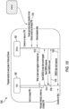
- FIGURE 6 is a block diagram of hardware further illustrating the host/slave SDIO configuration of FIGURE 2 , including special event hardware registers in a target device side, according to aspects of the present disclosure.
- an SD host 600 includes a host CPU 602 and an SD host controller (SDHC) host hardware (HW) 610.
- the SD host 600 is communicably coupled to an SD client device 630 through an SD bus 620.
- the SD client device 630 includes a client CPU 632 as well as SDIO client hardware (HW) 640.
- a host event register (HER) 652 and a client event register (CER) 654 are added to a client register space 650.
- a host function address space 660 includes a host event register (HER) 662 and a client event register (CER) 664.
- the host event register 662 and the client event register 654 maintain synchronization between the SD host 600 and the SD client device 630 to avoid the transaction timeout scenarios shown in FIGURES 4 and 5 .
- the host event register 662 and the client event register 654 are configured to raise an interrupt to the SD client device 630 or the SD host 600, respectively. For example, if the SD client device 630 wants to interrupt the SD host 600, the SD client device 630 writes to the client event register 654. In response, the SD host 600 sends an SD direct command (e.g., CMD52) to read the client event register 664 in the host function address space 660. Reading of the client event register 664 automatically clears the interrupt. When the SD host 600 wants to interrupt the SD client device 630, the SD host 600 writes to the host event register 662. In this example, the SD client device 630 is responsible for manually clearing the interrupt.
- CMD52 an SD direct command
- the host event register 662 and the client event register 654 are configured to raise an interrupt to the corresponding receiver (e.g., the host event register 652 or the client event register 664) whenever these registers are populated with valid data.
- the SD host 600 can write to the host event register 662 and read from the client event register 664 using the SD direct command (e.g., CMD52) to the host function address space 660.
- the SD client device 630 directly reads from the host event register 652 and directly writes to the client event register 654 in the client register space 650.
- client event/host event registers can vary from one byte to some maximum value depending on the use case. It should be recognized that design of the client event/host event registers with a minimal size is recommended to achieve maximum advantage. Additionally, the client event/host event registers may be a single register or a first-in-first-out (FIFO) type of register to support pipelining of the data requests, depending on the specifications. Optionally, additional data registers may be specified to carry additional metadata information along with the events.
- FIFO first-in-first-out
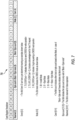
- FIGURE 7 is a block diagram illustrating an event register format, according to aspects of the present disclosure.
- an event register format 700 is shown using a 32-bit format; however, it should be recognized that other sizes for the event register format 700 are possible.
- the event register format 700 includes the following fields: (1) Event [0:3]; (2) Mode [4:5]; (3) Count [6:14]; (4) Byte count [15:23]; and (5) Reserved [24:31].
- the event field may provide a four-bit event identification (ID), which may have a predetermined meaning.
- ID event identification
- the four-bit event ID may indicate a transmit event (TX EVENT), a transmit acknowledgement event (TX_ACK_EVENT), or a receive event (RX_EVENT).
- the TX_EVENT ID may indicate the SD host 600 is about to send an SD direct command (e.g., CMD53) for a write operation.
- the RX_EVENT ID may indicate the SD client device 630 is requesting an SD direct command (e.g., CMD53) for a read operation.
- the TX_ACK_EVENT ID may indicate an acknowledgement from the SD client device 630 of a TX_EVENT ID, in which the SD client device 630 is requesting the SD direct command for a write operation from the SD host 600.
- the two-bit mode field may indicate the following modes: (1) Invalid Mode; (2) Byte Mode; (3) Block Mode; and (4) Block + Byte Mode.
- the fourth mode (e.g., Block + Byte Mode) may enable combining a block with additional bytes in a single data transaction.
- the event register format 700 also includes a nine-bit count field (e.g., Count [6: 14]).
- the nine-bit count field may indicate either a block or a byte count based on the Mode [4:5] field.
- the event register format 700 further includes a nine-bit byte count field (e.g., Byte count [15:23]).
- a reserved field e.g., Reserved [24:31] is a nine-bit field reserved for further expansion.
- FIGURE 8 is a timing diagram further illustrating the host/slave SDIO configuration of FIGURE 2 during a successful data transfer process due to communication to/from a target device, in accordance with aspects of the present disclosure.
- FIGURE 8 illustrates a method 800 of improving device synchronization over a secure digital (SD) bus between the SD host 600 and the SD client device 630.
- SD secure digital
- the SD client device 630 In the SDIO protocol, the SD client device 630 conventionally cannot communicate a current capability to accept incoming transmit data.
- the host event register 662 and the client event register 654 enable communication between the SD client device 630 and the SD host 600. This communication may prevent timeout of data transactions incurred when the SD client device 630 is a low speed embedded (e.g., Internet-of-things (IOT)) device.
- IOT Internet-of-things
- the operating speed of the SD client device 330 may lead to a data preparation timeout. That is, the low speed of the SD client device 330 delays allocation of buffer space within the SD client device 330 to accommodate incoming packet data from the SD host 300.
- the SD host 600 compensates for the SD client device 630, which is operating in a low power mode (LPM)/sleep mode.
- the SD host 600 compensates for the SD client device 630 by sending an SD direct command to write (e.g., CMD52 write command) the host event register 662 to raise an interrupt to the SD client device 630 at time 810 of the method 800 for improving synchronization. That is, rather than issue an SD extended command (e.g., CMD53) as performed in FIGURE 5 , the SD host 600 writes to the host event register 662 using the SD direct command (e.g., CMD52) to interrupt the SD client device 630. In this example, the interrupt wakes the SD client device 630, which comes out of sleep mode after a predetermined time period (t).
- the SD client device 630 receives the interrupt, and performs a data initialization process.
- the SD client device 630 is not in sleep mode (see FIGURE 4 ) when the interrupt is received. This interrupt notifies the SD client device 630 to initiate the data initialization process to prevent the timeout of the transaction, as shown in FIGURE 4 .
- the interrupt from the SD host 600 compensates for a low speed of the SD client device 630 by providing a head start with the data initialization process.
- the SD client device 630 raises an interrupt to the SD host 600 by writing to the client event register 654. This host interrupt informs the SD host 600 that the SD client device 630 is ready to receive write data.
- the SD host 600 sends the SD direct command (e.g., CMD52) to read the client event register 664, which clears the host interrupt to the SD host 600.
- the SD direct command response is received.
- the SD host 600 sends the SD extended command (e.g., CMD53) to write data to the SD client device 630.
- This process is completed at time 820, when an SD extended command response (e.g., CMD53) is received by the SD host 600 as notification of a successful data write transaction.
- the SD client device 630 is ready before the SD host 600 sends an SD extended command (e.g., CMD53 write request). As a result, this data write transaction will not time out due to a low speed target device or a sleep/low power mode of the SD client device 630.
- the addition of the host event register 652 and the client event register 654 to the client register space 650 enables the SD client device 630 to interrupt the SD host 600 for the SD extended command (e.g., the CMD53 write request).
- adding the host event register 662 and the client event register 664 to the host function address space 660 of the SD host 600 enables communication between the SD host 600 and the SD client device 630 before an SD extended command (e.g., CMD53 read/write request).
- the host event register 662 and the client event register 654 may also prevent timeout of low speed embedded (e.g., Internet-of-things (IOT)) devices (see FIGURE 4 ).
- IOT Internet-of-things
- the SD host 600 writes to the host event register 662 to wake up the target when operating in a low power mode (LPM), as shown in FIGURE 8 .
- LPM low power mode
- FIGURES 9A and 9B are block diagrams illustrating pipelined processing of read/write requests between host and target devices, according to aspects of the present disclosure.
- FIGURE 9A is a block diagram illustrating an existing implementation 900 in which an SD host has multiple data streams for an SD client device, performed in a predetermined first amount of time T1.
- the SD host sends an SD extended command (e.g., CMD53) for the read/write request.
- the CMD53 command is sent through a command (CMD) line (e.g., CMD LINE 904) and the SD client device sends a CMD53 response (RESP) on the CMD LINE 904.
- CMD command
- RESP CMD53 response
- the RESP is followed by metadata (M_DATA) on a DATA LINE 902, which performed in a predetermined time, referred to as a metadata exchange delay (t1).
- M_DATA metadata
- the SD host After decoding the M_DATA, the SD host sends a CMD53 command to read/write data on the CMD LINE 904 and receives a CMD read/write response (RESP) on the CMD LINE 904.
- RESP CMD read/write response
- the ACTUAL DATA1 is subsequently received on the DATA LINE 902.
- FIGURE 9B is a block diagram illustrating a proposed implementation 950 to efficiently support multiple data streams between an SD host and an SD client device.
- the SDIO protocol provides the CMD52 command (e.g., SD direct command) to transact one byte between the SD host 600 and the SD client device 630 using only the command (CMD) pin of the SD bus (see FIGURE 2 ).
- the SDIO protocol conventionally prohibits the CMD52 command from being simultaneously active (e.g., performed in parallel) with the CMD53 command on the SD bus.
- standard SD host drivers e.g., Linux standard SD host drivers
- CMD53 command is active on the SD bus 220.
- abort command is unblocked during an active CMD53 command. This abort command may be sent simultaneously with the CMD53 command for special handling.
- an SD host driver is modified to enable activation of a CMD52 command simultaneously with an active CMD53 command on an SD bus, as desired.
- This simultaneous activation of the CMD52 and CMD53 commands on the SD bus 620 conforms with the SD specification of the SDIO protocol.
- the SD host driver of the SD host 600 is provided with two independent channels for communicating with the SD client device 630.
- a meta-channel may refer to a CMD52 channel
- a data-channel may refer to a CMD53 channel.
- the SD host can send a CMD52 to the SD client device to prepare a next data transaction during a current data transaction.
- the SD client device prepares a buffer and informs the SD host to transfer/receive data when the current data transaction is complete.
- the proposed implementation 950 significantly improves performance.
- three packets of data e.g., ACTUAL DATA1, ACTUAL DATA2, and ACTUAL DATA3 are exchanged over the DATA LINE 902.
- the metadata exchange delay of the proposed implementation 950 is limited to the first data packet because the subsequent CMD52 and RESP are performed in parallel with the previous data transaction. That is, metadata exchanged using CMD52 for a next transaction can run in parallel to the previous data transaction (e.g., ACTUAL DATA1) for a continuous chunk of pipelined data traffic. In this scenario, approximately 426.7 microseconds are saved for the three-packet example shown, which would increase exponentially for an N packet pipeline of data traffic.
- the SD host initiates data transactions, however, there is no mechanism in which the SD client device can interrupt the SD host. Therefore, during conventional operation, the SD host frequently polls the SD client device to check whether any data is available. This polling leads to frequent waking of the SD client device (e.g., during low power mode (LPM)/sleep mode). In addition, the SD host continues to run as it waits for the SD client device to wake and provide a response. That is, when the SD client device is in the LPM/sleep mode, the SD client device first recovers from the LPM/sleep mode and then responds to the SD host, which wastes power when no data is available.
- LPM low power mode
- FIGURE 10 is a timing diagram further illustrating the host/slave SDIO configuration of FIGURE 2 for a data transfer process 1000 during LPM/sleep mode of both a host device and/or a target device, in accordance with aspects of the present disclosure.
- both the SD host 600 and the SD client device 630 are in LPM/sleep mode when the SD client device 630 receives data for the SD host 600 at time 1010 (e.g., from the Internet).
- the SD client device 630 prepares the data and informs the SD host 600 at time 1012 using a client event register (CER) to interrupt the SD host 600 to wake from LPM/sleep mode.
- CER client event register
- the SD client device 630 informs the SD host 600 that the SD client device 630 has data for the SD host 600 by writing to the client event register 654.
- the SD host 600 sends an SD direct command (e.g., CMD52) to read the client event register 664 from the host function address space 660 and interpret the contents of the client event register 664, at time 1014.
- a response to the SD direct command (e.g., CMD52) is received at time 1016.
- the SD host 600 sends an SD extended command (e.g., CMD53) to read the data from the SD client device 630.
- a response to the SD extended command (e.g., CMD53) is received at time 1020 to complete the process.
- the data transfer process 1000 enables both the SD client device 630 and the SD host 600 to operate in an LPM/sleep mode for an increased amount of time by avoiding polling of the SD client device 630.
- This data transfer process 1000 therefore, saves power for both the SD client device 630 and the SD host 600.
- the SD host 600 awakens for 50ms each second to check if the SD client device 630 has any available data to send the SD host 600. This process may consume a total of 20.53 mA per second.
- the data transfer process 1000 avoids polling, thereby limiting energy consumption to 5.59 mA per second. This results in approximately a 74% energy savings when data is unavailable.
- preventing timeout of low speed embedded devices as well as LPM/sleep mode devices may improve boot-loader hardware to expedite device boot-up. For example, data transactions cannot start until both the SD host 600 and SD client device 630 have completed their enumeration sequence as part of a device boot-up process. Unfortunately, there is no mechanism to notify the SD client device 630 whether the SD host 600 enumeration process is complete. In this target driven enumeration process, an application layer may hardcode a wait time for the SD client device 630. The hardcoded enumeration wait time, however, is undesirable.
- the SD client device 630 may error out due to an assumed problem on the host side.
- FIGURE 11 is a timing diagram further illustrating the host/slave SDIO configuration of FIGURE 2 for a device enumeration process 1100, in accordance with aspects of the present disclosure.
- an enumeration process time of the SD host 600 exceeds the enumeration process time of the SD client device 630.
- the enumeration process of the SD host 600 is complete.
- the SD host 600 writes to the host event register 662 at time 1112.
- the SD host 600 writes an event identification to the host event register 662, raising an interrupt to the SD client device 630.
- the SD client device 630 transitions from a wait state to an active state for proceeding with read/write transactions.
- the SD host 600 notifies the SD client device 630 that it has completed its enumerations sequence and is now ready to commence data transactions.
- This notification to the SD client device 630 is performed by writing to the host event register 662.
- This interrupt terminates a wait time (t2) for completion of an enumeration sequence of the SD client device 630, which is less than a worst case (e.g., hardcoded) wait time (t1).
- the SD host 600 populates the host event register 662 with a doorbell event identification (ID).
- ID doorbell event identification
- the SD client device 630 receives the interrupt, reads the host event register 652 from the client register space 650, and decodes the event ID.
- both the SD client device 630 and the SD host 600 are free to initiate a read/write data transaction.
- a CMD53 write request is issued by the SD host 600 at time 1118, after sending the CMD52 command to read the client event register 664 at time 1114, and sending the CMD52 response at time 1116.
- a CMD53 data write response is finally sent at time 1120.
- FIGURE 12 is a timing diagram further illustrating the host/slave SDIO configuration of FIGURE 2 for a target device error process 1200, in accordance with aspects of the present disclosure.
- an error scenario at a target side e.g., could be due to data loss, CRC (cyclic redundancy check) error or SW (software) error
- CRC cyclic redundancy check
- SW software error
- an application running on a host side performs an error recovery process.
- the error recovery process may involve a shutdown or performing actions for specific errors.
- the client event register 654 provides a mechanism to notify the SD host 600 about the error at time 1210.
- the SD client device 630 writes to the client event register 654, including a detected error code as well as an error code event ID.
- the SD host 600 sends a CMD52 read command to read the client event register 664, with a CMD52 read response received at time 1216.
- the SD host 600 performs a predetermined action based on the error code read from the client event register 664.
- FIGURE 13 is a flow diagram illustrating a method 1300 of improving synchronization over a secure digital (SD) bus between an SD host and an SD client device, according to aspects of the present disclosure.
- a client event register is written to interrupt the SD host for an SD extended command.
- the SD client device 630 writes to the client event register 654 at time 1012.
- the SD client device 630 which cannot issue SD commands (e.g., CMD52 and CMD53), has write access to the client event register 654 and read access to the host event register 652 because these registers are newly added to the client register space 650 shown in FIGURE 6 .
- the SD host is triggered to issue the SD direct command to the SD client device over the SD bus by the SD client device writing to the client event register.
- the SD host 600 issues the CMD53 command to read data from the SD client device 630 at time 1018.
- the SD host 600 is triggered to send the CMD53 command to write data to the SD client device 630 at time 818 by the SD client device 630 writing to the client event register 654 at time 812.
- the SD client device awakens in response to an interrupt received from the SD host through a host event register of the SD client device.
- the SD host 600 wakes the SD client device 630 from an LPM/sleep mode by sending a CMD52 command to write the host event register 662 to raise an interrupt to the SD client device 630 at time 810.
- This example compensates for the LPM/sleep mode of the SD client device 630 delaying a CMD53 write command until the SD host 600 first writes to the host event register 662 to interrupt and wake the SD client device 630.
- the interrupt wakes the SD client device 630, which prevents timeout of the data transaction of FIGURE 5 .
- One aspect of the present disclosure describes an apparatus for improving synchronization over a secure digital (SD) bus between an SD host and an SD client device including means for writing to a client event register to interrupt the SD host for an SD extended command.
- the apparatus also includes means for triggering the SD host to issue the SD extended command to the SD client device over the SD bus in response to the SD client device writing to the client event register.
- the trigger means may be the CPU 102, the GPU 104, the DSP 106, the NPU 108, and/or the memory 118 of a client/slave device 230 .
- the aforementioned means may be any module or apparatus configured to perform the functions recited by the aforementioned means.
- the methodologies may be implemented with modules (e.g., procedures, functions, and so on) that perform the described functions.
- Any machine-readable medium tangibly embodying instructions may be used in implementing the methodologies described.
- software codes may be stored in a memory and executed by a processor unit.
- Memory may be implemented within the processor unit or external to the processor unit.
- memory refers to any type of long term, short term, volatile, nonvolatile, or other memory and is not to be limited to any particular type of memory or number of memories, or type of media upon which memory is stored.
- the functions may be stored as one or more instructions or code on a non-transitory computer-readable medium.
- Examples include computer-readable media encoded with a data structure and computer-readable media encoded with a computer program.
- Computer-readable media includes physical computer storage media. A storage medium may be an available medium that can be accessed by a computer.
- Such computer-readable media can include RAM, ROM, EEPROM, CD-ROM or other optical disk storage, magnetic disk storage or other magnetic storage devices, or other medium that can be used to store desired program code in the form of instructions or data structures and that can be accessed by a computer.
- Disk and disc include compact disc (CD), laser disc, optical disc, digital versatile disc (DVD) and Blu-ray disc where disks usually reproduce data magnetically, while discs reproduce data optically with lasers. Combinations of the above should also be included within the scope of computer-readable media.
- instructions and/or data may be provided as signals on transmission media included in a communications apparatus.
- a communications apparatus may include a transceiver having signals indicative of instructions and data. The instructions and data are configured to cause one or more processors to implement the functions outlined in the claims.
- DSP digital signal processor
- ASIC application specific integrated circuit
- FPGA field programmable gate array
- a general-purpose processor may be a microprocessor, but, in the alternative, the processor may be any conventional processor, controller, microcontroller, or state machine.
- a processor may also be implemented as a combination of computing devices, e.g., a combination of a DSP and a microprocessor, multiple microprocessors, one or more microprocessors in conjunction with a DSP core, or any other such configuration.
- a software module may reside in RAM, flash memory, ROM, EPROM, EEPROM, registers, hard disk, a removable disk, a CD-ROM, or any other form of storage medium known in the art.
- An exemplary storage medium is coupled to the processor such that the processor can read information from, and write information to, the storage medium.
- the storage medium may be integral to the processor.
- the processor and the storage medium may reside in an ASIC.
- the ASIC may reside in a user terminal.
- the processor and the storage medium may reside as discrete components in a user terminal.
- the functions described may be implemented in hardware, software, firmware, or any combination thereof. If implemented in software, the functions may be stored on or transmitted over as one or more instructions or code on a computer-readable medium.
- Computer-readable media includes both computer storage media and communications media including any medium that facilitates transfer of a computer program from one place to another.
- a storage media may be any available media that can be accessed by a general-purpose or special-purpose computer.
- such computer-readable media can include RAM, ROM, EEPROM, CD-ROM or other optical disk storage, magnetic disk storage or other magnetic storage devices, or any other medium that can be used to carry or store specified program code means in the form of instructions or data structures and that can be accessed by a general-purpose or special-purpose computer, or a general-purpose or special-purpose processor. Also, any connection is properly termed a computer-readable medium.
- Disk and disc include compact disc (CD), laser disc, optical disc, digital versatile disc (DVD) and Blu-ray disc, where disks usually reproduce data magnetically, while discs reproduce data optically with lasers. Combinations of the above should also be included within the scope of computer-readable media.
Landscapes
- Engineering & Computer Science (AREA)
- Theoretical Computer Science (AREA)
- General Engineering & Computer Science (AREA)
- Software Systems (AREA)
- Physics & Mathematics (AREA)
- General Physics & Mathematics (AREA)
- Computer Hardware Design (AREA)
- Multimedia (AREA)
- Information Transfer Systems (AREA)
- Communication Control (AREA)
Claims (15)
- Ein Verfahren (1300) zum Verbessern von Synchronisation über einen SD-Bus (SD = secure digital) (620) zwischen einem SD-Host (600) und einer SD-Client-Einrichtung (630), wobei das Verfahren Folgendes aufweist:Schreiben (1302) in ein Client-Ereignisregister (654) zum Unterbrechen des SD-Hosts (600) für einen erweiterten SD-Befehl;Veranlassen (1304) des SD-Hosts den erweiterten SD-Befehl an die SD-Client-Einrichtung (630) über den SD-Bus (620) auszugeben ansprechend darauf, dass die SD-Client-Einrichtung (630) in das Client-Ereignisregister (654) schreibt; dadurch gekennzeichnet, dass es weiter Folgendes aufweist:Empfangen von Schreibmetadaten über eine Befehls- bzw. CMD-Leitung (CMD = command) des SD-Busses (620), von dem SD-Host (600) an die SD-Client-Einrichtung (630), um die SD-Client-Einrichtung (630) hinsichtlich einer nächsten Datentransaktion, die von dem SD-Host (600) verfügbar ist, zu benachrichtigen; undDurchführen eines Dateninitialisierungsprozesses für die nächste Datentransaktion während einer aktuellen Datentransaktion.
- Verfahren (1300) nach Anspruch 1, das weiter Folgendes aufweist:Initiieren, durch die SD-Client-Einrichtung (630), eines Dateninitialisierungsprozesses ansprechend auf eine Unterbrechung bzw. einen Interrupt von dem SD-Host (600) durch ein Host-Ereignisregister (662) der SD-Client-Einrichtung (630); undSchreiben in das Client-Ereignisregister (654) um den SD-Host (600) zu veranlassen den erweiterten SD-Befehl auszugeben, wenn der Dateninitialisierungsprozess abgeschlossen ist.
- Verfahren (1300) nach Anspruch 2, das weiter Folgendes aufweist:Lesen von Schreibdatenpaketen über Datenleitungen des SD-Busses (620) von dem SD-Host (600); undSpeichern der Schreibdatenpakete in einem Client-Puffer, der gemäß dem Dateninitialisierungsprozess zugeteilt ist.
- Verfahren (1300) nach Anspruch 1, das weiter Aufwecken der SD-Client-Einrichtung (630) aufweist ansprechend auf einen Interrupt, der von dem SD-Host (600) durch ein Host-Ereignisregister (662) der SD-Einrichtung (630) empfangen wird.
- Verfahren (1300) nach Anspruch 1, in dem der erweiterte SD-Befehl einen CMD53-Lesebefehl oder einen CMD53-Schreibbefehl aufweist.
- Verfahren (1300) nach Anspruch 1, das weiter Schreiben in das Client-Ereignisregister (654) aufweist zum Verursachen eines Interrupts von der SD-Client-Einrichtung (630), um den SD-Host (600) bezüglich Daten zu benachrichtigen, die von der SD-Client-Einrichtung (630) verfügbar sind.
- Verfahren (1300) nach Anspruch 1, das weiter Folgendes aufweist:Empfangen eines Interrupts von dem SD-Host (600) an dem Client-Ereignisregister der SD-Client-Einrichtung (630); undBeenden einer Aufzählungsverzögerungsperiode ansprechend auf den Interrupt von dem SD-Host (600).
- Verfahren (1300) nach Anspruch 1, das weiter Schreiben einer Fehlerereignisidentifikation bzw. Fehlerereignis-ID und eines Fehlercodes in das Client-Ereignisregister (654) aufweist.
- Verfahren (1300) nach Anspruch 1, das weiter Schreiben einer Türklingelereignisidentifikation bzw. -ID in das Client-Ereignisregister aufweist zum Aufwecken des SD-Hosts (600), um den SD-Host (600) zu benachrichtigen bezüglich Daten, die von der SD-Client-Einrichtung (630) verfügbar sind.
- Eine Vorrichtung, die konfiguriert ist zum Verbessern von Synchronisation über einen SD-Bus (SD = secure digital) (620), wobei die Vorrichtung Folgendes aufweist:ein Client-Ereignisregister (654); undeinen Prozessor (632), der an das Client-Ereignisregister (654) gekoppelt ist, wobei der Prozessor (632) konfiguriert ist:zum Schreiben in das Client-Ereignisregister (654) zum Unterbrechen eines SD-Hosts (600) für einen erweiterten SD-Befehl;zum Veranlassen des SD-Hosts (600) den erweiterten SD-Befehl an die Vorrichtung über den SD-Bus (620) auszugeben durch Schreiben in das Client-Ereignisregister (654); dadurch gekennzeichnet, dass sie weiter konfiguriert ist:zum Empfangen von Schreibmetadaten über eine Befehls- bzw. CMD-Leitung (CMD = command) des SD-Busses (620), von dem SD-Host (600) an die Vorrichtung, um die Vorrichtung hinsichtlich einer nächsten Datentransaktion, die von dem SD-Host (600) verfügbar ist, zu benachrichtigen; undzum Durchführen eines Dateninitialisierungsprozesses für die nächste Datentransaktion während einer aktuellen Datentransaktion.
- Vorrichtung nach Anspruch 10, in der der Prozessor (632) weiter konfiguriert ist:zum Initiieren eines Dateninitialisierungsprozesses ansprechend auf einen Interrupt von dem SD-Host (600) durch ein Host-Ereignisregister (662) der Vorrichtung; undzum Schreiben in das Client-Ereignisregister (654), wenn der Dateninitialisierungsprozess abgeschlossen ist zum Veranlassen des SD-Hosts (600), den erweiterten SD-Befehl auszugeben.
- Vorrichtung nach Anspruch 10, in der der Prozessor (632) weiter konfiguriert ist zum Aufwecken der Vorrichtung ansprechend auf einen Interrupt, der von dem SD-Host (600) durch ein Host-Ereignisregister (662) der Vorrichtung empfangen wird.
- Vorrichtung nach Anspruch 10, in der der erweiterte SD-Befehl einen CMD53-Lesebefehl oder einen CMD53-Schreibbefehl aufweist.
- Vorrichtung nach Anspruch 10, in der der Prozessor (632) weiter konfiguriert ist:zum Empfangen eines Interrupts von dem SD-Host (600) an dem Client-Ereignisregister (654) der Vorrichtung; undzum Beenden einer Aufzählungsverzögerungsperiode ansprechend auf den Interrupt von dem SD-Host (600).
- Vorrichtung nach Anspruch 10, in der der Prozessor (632) weiter konfiguriert ist zum Schreiben einer Türklingelereignisidentifikation bzw. -ID in das Client-Ereignisregister (654) zum Aufwecken des SD-Hosts (600), um den SD-Host (600) bezüglich Daten zu benachrichtigen, die von der Vorrichtung verfügbar sind.
Applications Claiming Priority (3)
| Application Number | Priority Date | Filing Date | Title |
|---|---|---|---|
| IN201941036366 | 2019-09-10 | ||
| US16/938,845 US11334402B2 (en) | 2019-09-10 | 2020-07-24 | SDIO chip-to-chip interconnect protocol extension for slow devices and power savings |
| PCT/US2020/043695 WO2021050167A1 (en) | 2019-09-10 | 2020-07-27 | Sdio chip-to-chip interconnect protocol extension for slow devices and power savings |
Publications (2)
| Publication Number | Publication Date |
|---|---|
| EP4028894A1 EP4028894A1 (de) | 2022-07-20 |
| EP4028894B1 true EP4028894B1 (de) | 2024-04-17 |
Family
ID=74849541
Family Applications (1)
| Application Number | Title | Priority Date | Filing Date |
|---|---|---|---|
| EP20754116.0A Active EP4028894B1 (de) | 2019-09-10 | 2020-07-27 | Sdio-chip-zu-chip-verbindungsprotokollerweiterung für langsame geräte und leistungseinsparung |
Country Status (5)
| Country | Link |
|---|---|
| US (1) | US11334402B2 (de) |
| EP (1) | EP4028894B1 (de) |
| CN (1) | CN114365104A (de) |
| TW (1) | TW202111559A (de) |
| WO (1) | WO2021050167A1 (de) |
Families Citing this family (1)
| Publication number | Priority date | Publication date | Assignee | Title |
|---|---|---|---|---|
| CN116320469B (zh) * | 2023-05-16 | 2024-03-01 | 摩尔线程智能科技(北京)有限责任公司 | 一种虚拟化视频编解码系统及方法、电子设备和存储介质 |
Family Cites Families (11)
| Publication number | Priority date | Publication date | Assignee | Title |
|---|---|---|---|---|
| US20060218324A1 (en) * | 2005-03-25 | 2006-09-28 | Matsushita Electrical Industrial Co., Ltd | Systems and methods for flexible data transfers in SDIO and/or MMC |
| TWI468969B (zh) * | 2005-10-18 | 2015-01-11 | Intertrust Tech Corp | 授權對電子內容作存取的方法及授權對該電子內容執行動作之方法 |
| US7827323B2 (en) * | 2006-12-08 | 2010-11-02 | Marvell Israel (M.I.S.L.) Ltd. | System and method for peripheral device communications |
| TWI353145B (en) | 2007-12-26 | 2011-11-21 | Ralink Technology Corp | Method for receiving data with sdio interface and |
| JP5372049B2 (ja) * | 2011-02-04 | 2013-12-18 | 株式会社東芝 | メモリシステム |
| JP5728292B2 (ja) * | 2011-02-04 | 2015-06-03 | 株式会社東芝 | メモリデバイス及びホストシステム |
| US8621122B2 (en) | 2011-04-07 | 2013-12-31 | Qualcomm Innovation Center, Inc. | Method and apparatus for transferring data |
| US9557802B2 (en) * | 2013-08-01 | 2017-01-31 | Mediatek Inc. | Method of controlling SDIO device and related SDIO system and SDIO device |
| US9442794B1 (en) * | 2013-11-22 | 2016-09-13 | Marvell International Ltd. | Methods and apparatus for accessing device memory via a host bus interface |
| US10127172B2 (en) * | 2015-06-22 | 2018-11-13 | Qualcomm Technologies International, Ltd. | Single SDIO interface with multiple SDIO units |
| US10114586B1 (en) * | 2017-06-22 | 2018-10-30 | Western Digital Technologies, Inc. | System and method for using host command data buffers as extended memory device volatile memory |
-
2020
- 2020-07-24 US US16/938,845 patent/US11334402B2/en active Active
- 2020-07-27 TW TW109125285A patent/TW202111559A/zh unknown
- 2020-07-27 CN CN202080062851.2A patent/CN114365104A/zh active Pending
- 2020-07-27 WO PCT/US2020/043695 patent/WO2021050167A1/en not_active Ceased
- 2020-07-27 EP EP20754116.0A patent/EP4028894B1/de active Active
Also Published As
| Publication number | Publication date |
|---|---|
| US11334402B2 (en) | 2022-05-17 |
| EP4028894A1 (de) | 2022-07-20 |
| WO2021050167A1 (en) | 2021-03-18 |
| US20210073053A1 (en) | 2021-03-11 |
| TW202111559A (zh) | 2021-03-16 |
| CN114365104A (zh) | 2022-04-15 |
Similar Documents
| Publication | Publication Date | Title |
|---|---|---|
| US10551906B2 (en) | Methods and apparatus for running and booting inter-processor communication link between independently operable processors | |
| US11176068B2 (en) | Methods and apparatus for synchronizing uplink and downlink transactions on an inter-device communication link | |
| EP4002137B1 (de) | Sicherer digitaler (sd) direktbefehl zur verbesserung des durchsatzes mit einem reduzierten speicherbedarf | |
| CN105224482A (zh) | 一种fpga加速卡高速存储系统 | |
| US20080046608A1 (en) | Low-Power Extended USB Flash Device Without Polling | |
| WO2012110798A1 (en) | Serial interface | |
| US8745296B2 (en) | Serial storage protocol compatible frame conversion, at least in part being compatible with SATA and one packet being compatible with PCIe protocol | |
| CN115499505B (zh) | Usb网卡和通信方法 | |
| CN104115467B (zh) | 通过多个桥元件在设备之间的通信桥接 | |
| CN117093157B (zh) | 一种用于单向光传输的ddr高速读写方法及系统 | |
| EP2207101A1 (de) | Methode und Vorrichtung für eine parallele Schnittstelle | |
| CN104021097A (zh) | 数据传输方法、装置及直接存储器存取 | |
| CN115437983A (zh) | 高速外围组件互连(PCIe)接口装置及其操作方法 | |
| CN116627869A (zh) | 应用于电子设备的数据传输方法及装置 | |
| US11334402B2 (en) | SDIO chip-to-chip interconnect protocol extension for slow devices and power savings | |
| US8621122B2 (en) | Method and apparatus for transferring data | |
| CN106027349A (zh) | 一种pci-e总线接口传输卡及基于该传输卡的数据传输方法 | |
| US12411797B2 (en) | Interrupt latency and error resilient full-duplex SPI driver | |
| CN117880364B (zh) | 一种数据传输方法、系统以及相关装置 | |
| CN101266583B (zh) | 一种存储卡总线操作方法 | |
| JP2000348004A (ja) | シリアル通信システム |
Legal Events
| Date | Code | Title | Description |
|---|---|---|---|
| STAA | Information on the status of an ep patent application or granted ep patent |
Free format text: STATUS: UNKNOWN |
|
| STAA | Information on the status of an ep patent application or granted ep patent |
Free format text: STATUS: THE INTERNATIONAL PUBLICATION HAS BEEN MADE |
|
| PUAI | Public reference made under article 153(3) epc to a published international application that has entered the european phase |
Free format text: ORIGINAL CODE: 0009012 |
|
| STAA | Information on the status of an ep patent application or granted ep patent |
Free format text: STATUS: REQUEST FOR EXAMINATION WAS MADE |
|
| 17P | Request for examination filed |
Effective date: 20220201 |
|
| AK | Designated contracting states |
Kind code of ref document: A1 Designated state(s): AL AT BE BG CH CY CZ DE DK EE ES FI FR GB GR HR HU IE IS IT LI LT LU LV MC MK MT NL NO PL PT RO RS SE SI SK SM TR |
|
| DAV | Request for validation of the european patent (deleted) | ||
| DAX | Request for extension of the european patent (deleted) | ||
| REG | Reference to a national code |
Ref country code: DE Ref legal event code: R079 Free format text: PREVIOUS MAIN CLASS: G06F0013420000 Ipc: G06F0013400000 Ref country code: DE Ref legal event code: R079 Ref document number: 602020029205 Country of ref document: DE Free format text: PREVIOUS MAIN CLASS: G06F0013420000 Ipc: G06F0013400000 |
|
| RIC1 | Information provided on ipc code assigned before grant |
Ipc: G06F 13/42 20060101ALI20230928BHEP Ipc: G06F 13/40 20060101AFI20230928BHEP |
|
| GRAP | Despatch of communication of intention to grant a patent |
Free format text: ORIGINAL CODE: EPIDOSNIGR1 |
|
| STAA | Information on the status of an ep patent application or granted ep patent |
Free format text: STATUS: GRANT OF PATENT IS INTENDED |
|
| INTG | Intention to grant announced |
Effective date: 20231108 |
|
| GRAS | Grant fee paid |
Free format text: ORIGINAL CODE: EPIDOSNIGR3 |
|
| GRAA | (expected) grant |
Free format text: ORIGINAL CODE: 0009210 |
|
| STAA | Information on the status of an ep patent application or granted ep patent |
Free format text: STATUS: THE PATENT HAS BEEN GRANTED |
|
| AK | Designated contracting states |
Kind code of ref document: B1 Designated state(s): AL AT BE BG CH CY CZ DE DK EE ES FI FR GB GR HR HU IE IS IT LI LT LU LV MC MK MT NL NO PL PT RO RS SE SI SK SM TR |
|
| REG | Reference to a national code |
Ref country code: GB Ref legal event code: FG4D |
|
| REG | Reference to a national code |
Ref country code: CH Ref legal event code: EP |
|
| REG | Reference to a national code |
Ref country code: IE Ref legal event code: FG4D Ref country code: DE Ref legal event code: R096 Ref document number: 602020029205 Country of ref document: DE |
|
| REG | Reference to a national code |
Ref country code: LT Ref legal event code: MG9D |
|
| REG | Reference to a national code |
Ref country code: NL Ref legal event code: MP Effective date: 20240417 |
|
| REG | Reference to a national code |
Ref country code: AT Ref legal event code: MK05 Ref document number: 1677919 Country of ref document: AT Kind code of ref document: T Effective date: 20240417 |
|
| PG25 | Lapsed in a contracting state [announced via postgrant information from national office to epo] |
Ref country code: NL Free format text: LAPSE BECAUSE OF FAILURE TO SUBMIT A TRANSLATION OF THE DESCRIPTION OR TO PAY THE FEE WITHIN THE PRESCRIBED TIME-LIMIT Effective date: 20240417 |
|
| PG25 | Lapsed in a contracting state [announced via postgrant information from national office to epo] |
Ref country code: NL Free format text: LAPSE BECAUSE OF FAILURE TO SUBMIT A TRANSLATION OF THE DESCRIPTION OR TO PAY THE FEE WITHIN THE PRESCRIBED TIME-LIMIT Effective date: 20240417 |
|
| PG25 | Lapsed in a contracting state [announced via postgrant information from national office to epo] |
Ref country code: IS Free format text: LAPSE BECAUSE OF FAILURE TO SUBMIT A TRANSLATION OF THE DESCRIPTION OR TO PAY THE FEE WITHIN THE PRESCRIBED TIME-LIMIT Effective date: 20240817 |
|
| PG25 | Lapsed in a contracting state [announced via postgrant information from national office to epo] |
Ref country code: BG Free format text: LAPSE BECAUSE OF FAILURE TO SUBMIT A TRANSLATION OF THE DESCRIPTION OR TO PAY THE FEE WITHIN THE PRESCRIBED TIME-LIMIT Effective date: 20240417 |
|
| PG25 | Lapsed in a contracting state [announced via postgrant information from national office to epo] |
Ref country code: FI Free format text: LAPSE BECAUSE OF FAILURE TO SUBMIT A TRANSLATION OF THE DESCRIPTION OR TO PAY THE FEE WITHIN THE PRESCRIBED TIME-LIMIT Effective date: 20240417 Ref country code: HR Free format text: LAPSE BECAUSE OF FAILURE TO SUBMIT A TRANSLATION OF THE DESCRIPTION OR TO PAY THE FEE WITHIN THE PRESCRIBED TIME-LIMIT Effective date: 20240417 |
|
| PG25 | Lapsed in a contracting state [announced via postgrant information from national office to epo] |
Ref country code: GR Free format text: LAPSE BECAUSE OF FAILURE TO SUBMIT A TRANSLATION OF THE DESCRIPTION OR TO PAY THE FEE WITHIN THE PRESCRIBED TIME-LIMIT Effective date: 20240718 |
|
| PG25 | Lapsed in a contracting state [announced via postgrant information from national office to epo] |
Ref country code: PT Free format text: LAPSE BECAUSE OF FAILURE TO SUBMIT A TRANSLATION OF THE DESCRIPTION OR TO PAY THE FEE WITHIN THE PRESCRIBED TIME-LIMIT Effective date: 20240819 |
|
| PG25 | Lapsed in a contracting state [announced via postgrant information from national office to epo] |
Ref country code: ES Free format text: LAPSE BECAUSE OF FAILURE TO SUBMIT A TRANSLATION OF THE DESCRIPTION OR TO PAY THE FEE WITHIN THE PRESCRIBED TIME-LIMIT Effective date: 20240417 |
|
| PG25 | Lapsed in a contracting state [announced via postgrant information from national office to epo] |
Ref country code: AT Free format text: LAPSE BECAUSE OF FAILURE TO SUBMIT A TRANSLATION OF THE DESCRIPTION OR TO PAY THE FEE WITHIN THE PRESCRIBED TIME-LIMIT Effective date: 20240417 |
|
| PG25 | Lapsed in a contracting state [announced via postgrant information from national office to epo] |
Ref country code: PL Free format text: LAPSE BECAUSE OF FAILURE TO SUBMIT A TRANSLATION OF THE DESCRIPTION OR TO PAY THE FEE WITHIN THE PRESCRIBED TIME-LIMIT Effective date: 20240417 |
|
| PG25 | Lapsed in a contracting state [announced via postgrant information from national office to epo] |
Ref country code: LV Free format text: LAPSE BECAUSE OF FAILURE TO SUBMIT A TRANSLATION OF THE DESCRIPTION OR TO PAY THE FEE WITHIN THE PRESCRIBED TIME-LIMIT Effective date: 20240417 |
|
| PG25 | Lapsed in a contracting state [announced via postgrant information from national office to epo] |
Ref country code: PT Free format text: LAPSE BECAUSE OF FAILURE TO SUBMIT A TRANSLATION OF THE DESCRIPTION OR TO PAY THE FEE WITHIN THE PRESCRIBED TIME-LIMIT Effective date: 20240819 Ref country code: PL Free format text: LAPSE BECAUSE OF FAILURE TO SUBMIT A TRANSLATION OF THE DESCRIPTION OR TO PAY THE FEE WITHIN THE PRESCRIBED TIME-LIMIT Effective date: 20240417 Ref country code: NO Free format text: LAPSE BECAUSE OF FAILURE TO SUBMIT A TRANSLATION OF THE DESCRIPTION OR TO PAY THE FEE WITHIN THE PRESCRIBED TIME-LIMIT Effective date: 20240717 Ref country code: LV Free format text: LAPSE BECAUSE OF FAILURE TO SUBMIT A TRANSLATION OF THE DESCRIPTION OR TO PAY THE FEE WITHIN THE PRESCRIBED TIME-LIMIT Effective date: 20240417 Ref country code: IS Free format text: LAPSE BECAUSE OF FAILURE TO SUBMIT A TRANSLATION OF THE DESCRIPTION OR TO PAY THE FEE WITHIN THE PRESCRIBED TIME-LIMIT Effective date: 20240817 Ref country code: HR Free format text: LAPSE BECAUSE OF FAILURE TO SUBMIT A TRANSLATION OF THE DESCRIPTION OR TO PAY THE FEE WITHIN THE PRESCRIBED TIME-LIMIT Effective date: 20240417 Ref country code: GR Free format text: LAPSE BECAUSE OF FAILURE TO SUBMIT A TRANSLATION OF THE DESCRIPTION OR TO PAY THE FEE WITHIN THE PRESCRIBED TIME-LIMIT Effective date: 20240718 Ref country code: FI Free format text: LAPSE BECAUSE OF FAILURE TO SUBMIT A TRANSLATION OF THE DESCRIPTION OR TO PAY THE FEE WITHIN THE PRESCRIBED TIME-LIMIT Effective date: 20240417 Ref country code: ES Free format text: LAPSE BECAUSE OF FAILURE TO SUBMIT A TRANSLATION OF THE DESCRIPTION OR TO PAY THE FEE WITHIN THE PRESCRIBED TIME-LIMIT Effective date: 20240417 Ref country code: BG Free format text: LAPSE BECAUSE OF FAILURE TO SUBMIT A TRANSLATION OF THE DESCRIPTION OR TO PAY THE FEE WITHIN THE PRESCRIBED TIME-LIMIT Effective date: 20240417 Ref country code: AT Free format text: LAPSE BECAUSE OF FAILURE TO SUBMIT A TRANSLATION OF THE DESCRIPTION OR TO PAY THE FEE WITHIN THE PRESCRIBED TIME-LIMIT Effective date: 20240417 Ref country code: RS Free format text: LAPSE BECAUSE OF FAILURE TO SUBMIT A TRANSLATION OF THE DESCRIPTION OR TO PAY THE FEE WITHIN THE PRESCRIBED TIME-LIMIT Effective date: 20240717 |
|
| PG25 | Lapsed in a contracting state [announced via postgrant information from national office to epo] |
Ref country code: DK Free format text: LAPSE BECAUSE OF FAILURE TO SUBMIT A TRANSLATION OF THE DESCRIPTION OR TO PAY THE FEE WITHIN THE PRESCRIBED TIME-LIMIT Effective date: 20240417 |
|
| REG | Reference to a national code |
Ref country code: DE Ref legal event code: R097 Ref document number: 602020029205 Country of ref document: DE |
|
| PG25 | Lapsed in a contracting state [announced via postgrant information from national office to epo] |
Ref country code: EE Free format text: LAPSE BECAUSE OF FAILURE TO SUBMIT A TRANSLATION OF THE DESCRIPTION OR TO PAY THE FEE WITHIN THE PRESCRIBED TIME-LIMIT Effective date: 20240417 |
|
| PG25 | Lapsed in a contracting state [announced via postgrant information from national office to epo] |
Ref country code: CZ Free format text: LAPSE BECAUSE OF FAILURE TO SUBMIT A TRANSLATION OF THE DESCRIPTION OR TO PAY THE FEE WITHIN THE PRESCRIBED TIME-LIMIT Effective date: 20240417 |
|
| PG25 | Lapsed in a contracting state [announced via postgrant information from national office to epo] |
Ref country code: SK Free format text: LAPSE BECAUSE OF FAILURE TO SUBMIT A TRANSLATION OF THE DESCRIPTION OR TO PAY THE FEE WITHIN THE PRESCRIBED TIME-LIMIT Effective date: 20240417 Ref country code: RO Free format text: LAPSE BECAUSE OF FAILURE TO SUBMIT A TRANSLATION OF THE DESCRIPTION OR TO PAY THE FEE WITHIN THE PRESCRIBED TIME-LIMIT Effective date: 20240417 |
|
| PG25 | Lapsed in a contracting state [announced via postgrant information from national office to epo] |
Ref country code: SM Free format text: LAPSE BECAUSE OF FAILURE TO SUBMIT A TRANSLATION OF THE DESCRIPTION OR TO PAY THE FEE WITHIN THE PRESCRIBED TIME-LIMIT Effective date: 20240417 |
|
| PG25 | Lapsed in a contracting state [announced via postgrant information from national office to epo] |
Ref country code: SM Free format text: LAPSE BECAUSE OF FAILURE TO SUBMIT A TRANSLATION OF THE DESCRIPTION OR TO PAY THE FEE WITHIN THE PRESCRIBED TIME-LIMIT Effective date: 20240417 Ref country code: SK Free format text: LAPSE BECAUSE OF FAILURE TO SUBMIT A TRANSLATION OF THE DESCRIPTION OR TO PAY THE FEE WITHIN THE PRESCRIBED TIME-LIMIT Effective date: 20240417 Ref country code: RO Free format text: LAPSE BECAUSE OF FAILURE TO SUBMIT A TRANSLATION OF THE DESCRIPTION OR TO PAY THE FEE WITHIN THE PRESCRIBED TIME-LIMIT Effective date: 20240417 Ref country code: EE Free format text: LAPSE BECAUSE OF FAILURE TO SUBMIT A TRANSLATION OF THE DESCRIPTION OR TO PAY THE FEE WITHIN THE PRESCRIBED TIME-LIMIT Effective date: 20240417 Ref country code: DK Free format text: LAPSE BECAUSE OF FAILURE TO SUBMIT A TRANSLATION OF THE DESCRIPTION OR TO PAY THE FEE WITHIN THE PRESCRIBED TIME-LIMIT Effective date: 20240417 Ref country code: CZ Free format text: LAPSE BECAUSE OF FAILURE TO SUBMIT A TRANSLATION OF THE DESCRIPTION OR TO PAY THE FEE WITHIN THE PRESCRIBED TIME-LIMIT Effective date: 20240417 |
|
| PG25 | Lapsed in a contracting state [announced via postgrant information from national office to epo] |
Ref country code: IT Free format text: LAPSE BECAUSE OF FAILURE TO SUBMIT A TRANSLATION OF THE DESCRIPTION OR TO PAY THE FEE WITHIN THE PRESCRIBED TIME-LIMIT Effective date: 20240417 Ref country code: MC Free format text: LAPSE BECAUSE OF FAILURE TO SUBMIT A TRANSLATION OF THE DESCRIPTION OR TO PAY THE FEE WITHIN THE PRESCRIBED TIME-LIMIT Effective date: 20240417 |
|
| PLBE | No opposition filed within time limit |
Free format text: ORIGINAL CODE: 0009261 |
|
| STAA | Information on the status of an ep patent application or granted ep patent |
Free format text: STATUS: NO OPPOSITION FILED WITHIN TIME LIMIT |
|
| REG | Reference to a national code |
Ref country code: CH Ref legal event code: PL |
|
| PG25 | Lapsed in a contracting state [announced via postgrant information from national office to epo] |
Ref country code: LU Free format text: LAPSE BECAUSE OF NON-PAYMENT OF DUE FEES Effective date: 20240727 |
|
| 26N | No opposition filed |
Effective date: 20250120 |
|
| PG25 | Lapsed in a contracting state [announced via postgrant information from national office to epo] |
Ref country code: LU Free format text: LAPSE BECAUSE OF NON-PAYMENT OF DUE FEES Effective date: 20240727 |
|
| PG25 | Lapsed in a contracting state [announced via postgrant information from national office to epo] |
Ref country code: BE Free format text: LAPSE BECAUSE OF NON-PAYMENT OF DUE FEES Effective date: 20240731 Ref country code: SI Free format text: LAPSE BECAUSE OF FAILURE TO SUBMIT A TRANSLATION OF THE DESCRIPTION OR TO PAY THE FEE WITHIN THE PRESCRIBED TIME-LIMIT Effective date: 20240417 Ref country code: CH Free format text: LAPSE BECAUSE OF NON-PAYMENT OF DUE FEES Effective date: 20240731 |
|
| REG | Reference to a national code |
Ref country code: BE Ref legal event code: MM Effective date: 20240731 |
|
| PGFP | Annual fee paid to national office [announced via postgrant information from national office to epo] |
Ref country code: GB Payment date: 20250612 Year of fee payment: 6 |
|
| PGFP | Annual fee paid to national office [announced via postgrant information from national office to epo] |
Ref country code: FR Payment date: 20250612 Year of fee payment: 6 |
|
| PG25 | Lapsed in a contracting state [announced via postgrant information from national office to epo] |
Ref country code: IE Free format text: LAPSE BECAUSE OF NON-PAYMENT OF DUE FEES Effective date: 20240727 |
|
| PG25 | Lapsed in a contracting state [announced via postgrant information from national office to epo] |
Ref country code: SE Free format text: LAPSE BECAUSE OF FAILURE TO SUBMIT A TRANSLATION OF THE DESCRIPTION OR TO PAY THE FEE WITHIN THE PRESCRIBED TIME-LIMIT Effective date: 20240417 |
|
| PGFP | Annual fee paid to national office [announced via postgrant information from national office to epo] |
Ref country code: DE Payment date: 20250616 Year of fee payment: 6 |
|
| PG25 | Lapsed in a contracting state [announced via postgrant information from national office to epo] |
Ref country code: CY Free format text: LAPSE BECAUSE OF FAILURE TO SUBMIT A TRANSLATION OF THE DESCRIPTION OR TO PAY THE FEE WITHIN THE PRESCRIBED TIME-LIMIT; INVALID AB INITIO Effective date: 20200727 |
|
| PG25 | Lapsed in a contracting state [announced via postgrant information from national office to epo] |
Ref country code: HU Free format text: LAPSE BECAUSE OF FAILURE TO SUBMIT A TRANSLATION OF THE DESCRIPTION OR TO PAY THE FEE WITHIN THE PRESCRIBED TIME-LIMIT; INVALID AB INITIO Effective date: 20200727 |