EP4027517A1 - Bulk acoustic wave resonator with piezoelectric layer having insert structure, and filter and electronic device - Google Patents
Bulk acoustic wave resonator with piezoelectric layer having insert structure, and filter and electronic device Download PDFInfo
- Publication number
- EP4027517A1 EP4027517A1 EP20859838.3A EP20859838A EP4027517A1 EP 4027517 A1 EP4027517 A1 EP 4027517A1 EP 20859838 A EP20859838 A EP 20859838A EP 4027517 A1 EP4027517 A1 EP 4027517A1
- Authority
- EP
- European Patent Office
- Prior art keywords
- layer
- resonator
- insertion layer
- resonator according
- piezoelectric layer
- Prior art date
- Legal status (The legal status is an assumption and is not a legal conclusion. Google has not performed a legal analysis and makes no representation as to the accuracy of the status listed.)
- Pending
Links
Images





Classifications
-
- H—ELECTRICITY
- H03—ELECTRONIC CIRCUITRY
- H03H—IMPEDANCE NETWORKS, e.g. RESONANT CIRCUITS; RESONATORS
- H03H3/00—Apparatus or processes specially adapted for the manufacture of impedance networks, resonating circuits, resonators
- H03H3/007—Apparatus or processes specially adapted for the manufacture of impedance networks, resonating circuits, resonators for the manufacture of electromechanical resonators or networks
- H03H3/02—Apparatus or processes specially adapted for the manufacture of impedance networks, resonating circuits, resonators for the manufacture of electromechanical resonators or networks for the manufacture of piezoelectric or electrostrictive resonators or networks
-
- H—ELECTRICITY
- H03—ELECTRONIC CIRCUITRY
- H03H—IMPEDANCE NETWORKS, e.g. RESONANT CIRCUITS; RESONATORS
- H03H9/00—Networks comprising electromechanical or electro-acoustic elements; Electromechanical resonators
- H03H9/02—Details
- H03H9/02007—Details of bulk acoustic wave devices
- H03H9/02086—Means for compensation or elimination of undesirable effects
- H03H9/02118—Means for compensation or elimination of undesirable effects of lateral leakage between adjacent resonators
-
- H—ELECTRICITY
- H03—ELECTRONIC CIRCUITRY
- H03H—IMPEDANCE NETWORKS, e.g. RESONANT CIRCUITS; RESONATORS
- H03H9/00—Networks comprising electromechanical or electro-acoustic elements; Electromechanical resonators
- H03H9/02—Details
- H03H9/02007—Details of bulk acoustic wave devices
- H03H9/02015—Characteristics of piezoelectric layers, e.g. cutting angles
-
- H—ELECTRICITY
- H03—ELECTRONIC CIRCUITRY
- H03H—IMPEDANCE NETWORKS, e.g. RESONANT CIRCUITS; RESONATORS
- H03H9/00—Networks comprising electromechanical or electro-acoustic elements; Electromechanical resonators
- H03H9/02—Details
- H03H9/02007—Details of bulk acoustic wave devices
- H03H9/02086—Means for compensation or elimination of undesirable effects
- H03H9/02102—Means for compensation or elimination of undesirable effects of temperature influence
-
- H—ELECTRICITY
- H03—ELECTRONIC CIRCUITRY
- H03H—IMPEDANCE NETWORKS, e.g. RESONANT CIRCUITS; RESONATORS
- H03H9/00—Networks comprising electromechanical or electro-acoustic elements; Electromechanical resonators
- H03H9/02—Details
- H03H9/02007—Details of bulk acoustic wave devices
- H03H9/02157—Dimensional parameters, e.g. ratio between two dimension parameters, length, width or thickness
-
- H—ELECTRICITY
- H03—ELECTRONIC CIRCUITRY
- H03H—IMPEDANCE NETWORKS, e.g. RESONANT CIRCUITS; RESONATORS
- H03H9/00—Networks comprising electromechanical or electro-acoustic elements; Electromechanical resonators
- H03H9/15—Constructional features of resonators consisting of piezoelectric or electrostrictive material
- H03H9/17—Constructional features of resonators consisting of piezoelectric or electrostrictive material having a single resonator
-
- H—ELECTRICITY
- H03—ELECTRONIC CIRCUITRY
- H03H—IMPEDANCE NETWORKS, e.g. RESONANT CIRCUITS; RESONATORS
- H03H9/00—Networks comprising electromechanical or electro-acoustic elements; Electromechanical resonators
- H03H9/15—Constructional features of resonators consisting of piezoelectric or electrostrictive material
- H03H9/17—Constructional features of resonators consisting of piezoelectric or electrostrictive material having a single resonator
- H03H9/171—Constructional features of resonators consisting of piezoelectric or electrostrictive material having a single resonator implemented with thin-film techniques, i.e. of the film bulk acoustic resonator [FBAR] type
-
- H—ELECTRICITY
- H03—ELECTRONIC CIRCUITRY
- H03H—IMPEDANCE NETWORKS, e.g. RESONANT CIRCUITS; RESONATORS
- H03H9/00—Networks comprising electromechanical or electro-acoustic elements; Electromechanical resonators
- H03H9/15—Constructional features of resonators consisting of piezoelectric or electrostrictive material
- H03H9/17—Constructional features of resonators consisting of piezoelectric or electrostrictive material having a single resonator
- H03H9/171—Constructional features of resonators consisting of piezoelectric or electrostrictive material having a single resonator implemented with thin-film techniques, i.e. of the film bulk acoustic resonator [FBAR] type
- H03H9/172—Means for mounting on a substrate, i.e. means constituting the material interface confining the waves to a volume
- H03H9/173—Air-gaps
-
- H—ELECTRICITY
- H03—ELECTRONIC CIRCUITRY
- H03H—IMPEDANCE NETWORKS, e.g. RESONANT CIRCUITS; RESONATORS
- H03H9/00—Networks comprising electromechanical or electro-acoustic elements; Electromechanical resonators
- H03H9/46—Filters
- H03H9/54—Filters comprising resonators of piezoelectric or electrostrictive material
Definitions
- Embodiments of the present disclosure relate to the field of semiconductors, and in particular, to a bulk acoustic wave resonator, a filter, and an electronic device having one of the bulk acoustic wave resonator and the filter.
- a bulk acoustic wave filter has been widely used in the current wireless communication systems due to its low insertion loss, high square coefficient, high power capacity and the like, and becomes an important component for determining quality of radio frequency signals received by or transmitted from the communication systems.
- Performance of the bulk acoustic wave filter is determined by a bulk acoustic wave resonator of the bulk acoustic wave filter. For example, a resonant frequency of the bulk acoustic wave resonator determines an operation frequency of the filter, an effective electromechanical coupling coefficient of the bulk acoustic wave resonator determines a bandwidth of the filter, and a quality factor of the bulk acoustic wave resonator determines insertion loss of the filter.
- a quality factor thereof especially the quality factor (or a series-parallel impedance) at a series resonant frequency and a parallel resonant frequency, will significantly affect a passband insertion loss. Therefore, it is important to improve the quality factor of the resonator when configuring the filter with high-performance.
- a quality factor (Qs) or series impedance (Rs) at the series resonant frequency of the bulk acoustic wave resonator is usually determined by electrode loss and material loss, and a quality factor (Qp) or parallel impedance (Rp) at the parallel resonant frequency of the bulk acoustic wave resonator is usually affected by boundary acoustic wave leakage.
- the boundary acoustic wave leakage may be effectively improved by changing a boundary structure of the resonator, thereby significantly improving the Qp (or Rp) of the resonator.
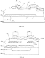
- FIG. 1A is a schematic structural sectional view of a conventional film bulk acoustic wave resonator.
- a reference sign 100 indicates a substrate
- a reference sign 110 indicates an acoustic mirror
- a reference sign 120 indicates a bottom electrode
- a reference sign 130 indicates a piezoelectric layer
- a reference sign 140 indicates a top electrode
- a reference sign 15 indicates an annular protruding structure
- a reference sign 16 indicates a wing structure
- a reference sign h1 indicates a height of a gap
- a reference sign h2 indicates a thickness of the protruding structure
- a reference sign 17 indicates a bridge structure.
- Reference signs d11-d14 indicate various dimensions.
- a composite structure is arranged at an edge of an effective region on an upper surface of the resonator. Accordingly, acoustic impedances on both sides of the edge of the effective region are not matched with each other, which limits propagation of transverse Lamb waves and enhances reflection and conversion capability to the Lamb waves, thereby improving the Rp.
- the piezoelectric layer has poor quality due to a rough edge of the bottom electrode at a connection side of the top electrode and the bottom electrode.
- the composite structure allows a resonance excitation caused by the piezoelectric layer with poor quality to contribute less to the entire circuit, and thus improves K t , eff 2 and anti-static discharge performance.
- FIG. 1B is a schematic structural sectional view of an existing film bulk acoustic wave resonator.
- a reference sign 100 indicates a substrate
- a reference sign 110 indicates an acoustic mirror
- a reference sign 120 indicates a bottom electrode
- a reference sign 130 indicates a piezoelectric layer
- a reference sign 140 indicates a top electrode
- a reference sign 160 indicates an annular protruding structure
- a reference sign h2 indicates a thickness of the protruding structure.
- Reference signs d12 and d18 indicate various dimensions.
- the annular protrusion 160 is a single-layer structure which may be made of a metal or a dielectric material, or may be formed by air.
- a single-layer insertion structure is arranged in the piezoelectric layer, and thus electrical properties of the resonator such as Rp can be improved.
- the energy leakage at the edge of the effective region of the resonator cannot be effectively improved, and the Rp thus cannot be effectively improved.
- the present disclosure is provided to further improve an Rp value or a Qp value of a bulk acoustic wave resonator.
- a bulk acoustic wave resonator is provided with a composite insertion structure arranged in the middle of a piezoelectric layer in an edge region of an effective region of the resonator.
- the composite insertion structure has an insertion protrusion corresponding to a first insertion layer and an insertion wing-bridge corresponding to a second insertion layer, thereby effectively increasing the Rp value of the bulk acoustic wave resonator.
- the bulk acoustic wave resonator includes a substrate, an acoustic mirror, a bottom electrode, a top electrode, and a piezoelectric layer.
- the acoustic mirror, the bottom electrode, the piezoelectric layer and the top electrode overlap with each other in a thickness direction of the substrate to form an overlapping region, and the overlapping region is an effective region of the resonator.
- the piezoelectric layer is provided with a composite insertion structure arranged along an edge of the effective region, and the composite insertion structure includes a first insertion layer and a second insertion layer. In a top view of the resonator, at least part of the first insertion layer overlaps with the effective region, and in the top view of the resonator, the first insertion layer at least partially overlaps with the second insertion layer.
- the first insertion layer is made of a metallic material and the second insertion layer is formed of air or made of a dielectric material, or the first insertion layer is made of a dielectric material and the second insertion layer is formed of air.
- the second insertion layer is arranged on the first insertion layer in a thickness direction of the resonator.
- the second insertion layer covers and surrounds the first insertion layer or covers a part of the first insertion layer.
- an outer end of a portion of the piezoelectric layer below the first insertion layer is arranged at an outer side of an outer end of a portion of the piezoelectric layer above the first insertion layer in a radial direction.
- an outer end of the top electrode is aligned with the outer end of the portion of the piezoelectric layer above the first insertion layer in the sectional view parallel to the thickness direction of the resonator.
- the first insertion layer is arranged on the second insertion layer in the thickness direction of the resonator.
- the first insertion layer covers and surrounds the second insertion layer or covers a part of the second insertion layer.
- an outer end of a portion of the piezoelectric layer below the first insertion layer is arranged at an outer side of an outer end of a portion of the piezoelectric layer above the first insertion layer in a radial direction.
- an outer end of the top electrode is aligned with the outer end of the portion of the piezoelectric layer above the first insertion layer and the outer end of the first insertion layer in the sectional view parallel to the thickness direction of the resonator.
- the second insertion layer, the first insertion layer and the effective region at least partially overlap with each other.
- the composite insertion structure is an annular insertion structure.
- the second insertion layer includes an insertion wing structure provided at a non-connection side of the electrodes in a top view of the resonator.
- the second insertion layer includes an insertion bridge structure provided at a connection side of the electrodes in a top view of the resonator.
- a distance between an outer end of the insertion bridge structure and an end of the bottom electrode is in a range of 0 to 20 um in a radial direction.
- the first insertion layer extends beyond the bottom electrode, a distance between an outer end of the first insertion layer and the end of the bottom electrode is in a range of 0 to 10 um in the radial direction, and the distance between the outer end of the insertion bridge structure and the end of the bottom electrode in the radial direction is greater than the distance between the outer end of the first insertion layer and the end of the bottom electrode in the radial direction.
- the first insertion layer overlapping with the effective region is a flat insertion portion.
- the first insertion layer is a flat layer protrusion.
- the first insertion layer includes the flat insertion portion and a protrusion step portion, and the protrusion step portion and the flat insertion portion form a step; and/or the second insertion layer includes a wing-bridge step portion.
- At least part of the composite insertion structure is arranged at a middle position of a corresponding portion of the piezoelectric layer in a thickness direction of the piezoelectric layer.
- a distance between an inner end of the first insertion layer and an inner end of the second insertion layer is in a range of 0 to 10 um.
- the first insertion layer, the second insertion layer and the effective region overlap with each other in a range of 0 to 10 um in the thickness direction of the resonator.
- the first insertion layer has a thickness in a range of 50 A to 5000 A
- the second insertion layer has a thickness in a range of 50 A to 5000 A.
- the metal material includes at least one of gold (Au), tungsten (W), molybdenum (Mo), platinum (Pt), ruthenium (Ru), iridium (Ir), titanium tungsten (TiW), aluminum (Al), titanium (Ti), osmium (Os), magnesium (Mg), gold (Au), tungsten (W), molybdenum (Mo), platinum (Pt), puthenium (Ru), iridium (Ir), germanium (Ge), copper (Cu), aluminum (Al), chromium (Cr), or arsenic doped gold.
- the dielectric material includes at least one of silicon dioxide (SiO2), silicon nitride (Si 3 N 4 ), silicon carbide (SiC), aluminum nitride (AlN), aluminum oxide (Al 2 O 3 ), porous silicon, fluorinated amorphous carbon, fluoropolymer, parylene, polyarylene ether, hydrogen silsesquioxane, cross-linked polyphenylene polymer, bisphenylcyclobutene, fluorinated silica, carbon-doped oxide, or diamond.
- silicon dioxide SiO2
- silicon nitride Si 3 N 4
- silicon carbide SiC
- AlN aluminum nitride
- Al 2 O 3 aluminum oxide
- porous silicon porous silicon
- fluorinated amorphous carbon fluoropolymer
- parylene parylene
- polyarylene ether polyarylene ether
- hydrogen silsesquioxane cross-linked polyphenylene polymer
- the first insertion layer and/or the second insertion layer span/spans a boundary of the effective region.
- the composite insertion structure is arranged between a first piezoelectric layer portion and a second piezoelectric layer portion, the first piezoelectric layer portion and the second piezoelectric layer portion form the piezoelectric layer, and a material of the first piezoelectric layer portion is different from a material of the second piezoelectric layer portion.
- a filter including the bulk acoustic wave resonator as described above.
- an electronic device including the bulk acoustic wave resonator as described above or the filter as described above.
- FIG. 2 is a schematic top view of a bulk acoustic wave resonator according to an exemplary embodiment of the present disclosure.
- the bulk acoustic wave resonator includes a bottom electrode, a piezoelectric layer, a top electrode, and a composite annular insertion structure.
- the top electrode may be covered with a passivation layer.
- the composite annular insertion structure is composed of an annular insertion protrusion structure and an annular insertion wing-bridge structure.
- the annular insertion wing-bridge structure is formed as an annular wing structure at a non-connection side of the bottom electrode and the top electrode, and formed as an annular bridge structure at a connection side of the top electrode and the bottom electrode.
- the composite insertion structure has a serrated shape.
- an actual shape of the composite insertion structure is not necessarily in a serrated shape.
- the composite insertion structure may have an edge shape parallel to an edge of the top electrode.
- the insertion structure may be annular or not, which all falls within the scope of the present disclosure.
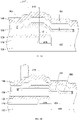
- FIG. 2A is a schematic partial sectional view of the bulk acoustic wave resonator along line O-A in FIG. 2 according to an exemplary embodiment of the present disclosure.
- the bulk acoustic wave resonator includes a substrate 100 and an acoustic mirror 110, which is located on an upper surface of the substrate or embedded in an interior thereof.
- the acoustic mirror is formed by a cavity embedded in the substrate, and any other acoustic mirror structures such as a Bragg reflector may also be applicable.
- the bulk acoustic wave resonator further includes a bottom electrode 120, a piezoelectric layer 130, a top electrode 140, an insertion protrusion 150, and an insertion wing 160. Further, the insertion protrusion 150 and the insertion wing 160 form a composite insertion structure.
- the top electrode 140 may be provided with a passivation layer.
- the bottom electrode 120 is deposited on an upper surface of the acoustic mirror and covers the acoustic mirror.
- the bottom electrode 120 may be etched into a bevel at an edge thereof, and the bevel is located outside the acoustic mirror. Further, the edge of the bottom electrode 120 may be etched into a stepped or vertical shape or other similar structures.
- the acoustic mirror 110, the bottom electrode 120, the piezoelectric layer 130 and the top electrode 140 overlap with each other to form an overlapping region, which is an effective region of the resonator.
- the top electrode is located inside the acoustic mirror with a distance d14 in a range of 0 to 10 um from an edge of the acoustic mirror.
- the bottom electrode is located outside the acoustic mirror. A distance between a first end of the bottom electrode and the acoustic mirror is d13, and d13 is in a range of 0 to 10 um.
- the insertion protrusion 150 has a first end (an inner end) and a second end (an outer end).
- a side close to a center of the effective region in a radial or lateral direction is defined as an inner side
- a side away from the center of the effective region in the radial or lateral direction is defined as an outer side.
- the first end of the insertion protrusion 150 is located at the inner side of the effective region.
- the second end of the insertion protrusion 150 is aligned with an edge of the effective region, or extends beyond the effective region by a distance d15 in a range of 0 to 20 um.
- the first end of the insertion protrusion 150 is spaced apart from a first end of the insertion wing 160 by a distance d11 in a range of 0 to 10 um.
- the insertion protrusion has a height h1 in a range of 50 A to 5000 A.
- the insertion wing 160 has the first end and a second end.
- the first end of the insertion wing 160 is located on the insertion protrusion 150 in a thickness direction, and is located between the edge of the effective region and the first end of insertion protrusion 150 in a horizontal direction.
- the second end of the insertion wing 160 is aligned with the edge of the effective region or extends beyond the effective region.
- the second end of the insertion wing 160 is spaced apart from the second end of the insertion protrusion 150 by a distance d16 in a range of 0 to 20 um.
- the first end of the insertion wing 160 is spaced apart from an edge of the top electrode 140 by a distance d12 in a range of 0 to 10 um.
- the insertion wing 160 has a height h2 in a range of 50 A to 5000 A.
- the numerical range may not only include end values of the numerical range, but also include a mean value or midpoint value within the numerical range.
- the insertion protrusion 150 is made of a metal, such as Mo, W, Cu, or Al.
- the insertion wing 160 is made of a dielectric material such as SiO 2 , Si 3 N 4 , ALN, doped AlN with a different doping concentration from the piezoelectric layer, or is formed of air.
- FIG. 2B is a schematic view of a position arrangement of the insertion protrusion in a thickness direction of the piezoelectric layer according to an exemplary embodiment of the present disclosure. More specifically, in the thickness direction of the resonator, the piezoelectric layer is divided equally into three parts by lines C-C and D-D. In addition, line E-E is defined as a horizontal central line of the insertion protrusion, and is located in the middle of contour lines shown by the lines C-C and D-D.
- the insertion protrusion may be arranged such that the insertion protrusion and the insertion wing overlap with each other to form an overlapping portion. In addition, such the overlapping portion may be formed in the piezoelectric layer.
- the insertion protrusion is arranged in the middle of the piezoelectric layer as long as the insertion protrusion is arranged between the lines C-C and D-D.
- a composite insertion layer (an insertion protruding layer corresponding to a first insertion layer and a wing-bridge layer corresponding to a second insertion layer) provided in the piezoelectric layer is located at a position where a stress is maximum in a resonator piston mode, which corresponds to a special arrangement in which the composite insertion layer is located in the middle of the piezoelectric layer. Accordingly, the resulting impedance mismatch has a stronger reflection effect on the acoustic waves.
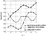
- FIG. 6 illustrates a simulation comparison result of an arrangement in which for example a metal insertion layer and an air insertion layer are provided according to an exemplary embodiment of the present disclosure versus an arrangement in which for example a single metal layer or a single air layer is provided.
- the present disclosure achieves a higher Rp value than the existing single-layer insertion structure.
- FIG. 2C is a schematic partial sectional view of the bulk acoustic wave resonator along line O-B in FIG. 2 according to an exemplary embodiment of the present disclosure.
- the bottom electrode extends beyond the acoustic mirror, and a distance d19 between an edge of the bottom electrode and the acoustic mirror is in a range of 0 to 10 um.
- the insertion protrusion 150 has a first end located inside the effective region and a second end aligned with the acoustic mirror. The first end of the insertion protrusion 150 is spaced apart from a first end of an insertion bridge 161 by a distance d17 in a range of 0 to 10 um.
- the insertion bridge 161 has the first end located on the insertion protrusion 150 in the thickness direction and a second end.
- the first end of the insertion bridge 161 is spaced apart from the edge of the acoustic mirror by a distance d18 in a range of 0 to 10 um.
- the second end of the insertion bridge 161 extends beyond the bottom electrode, and a distance d20 between the bottom electrode and the second end of the insertion bridge 161 is in a range of 0 to 20 um.
- FIG. 2D is a schematic partial sectional view of the bulk acoustic wave resonator along line O-B in FIG. 2 according to another exemplary embodiment of the present disclosure.
- the embodiment shown in FIG. 2D is similar to that shown in FIG. 2C except that the second end of the insertion protrusion 150 extends beyond the effective region with an extension amount d1.
- FIG. 2E is a schematic partial sectional view of the bulk acoustic wave resonator along line O-B in FIG. 2 according to a yet another exemplary embodiment of the present disclosure.
- the embodiment shown in FIG. 2E is similar to that shown in FIG. 2C except that the second end of the insertion protrusion structure 150 extends beyond the edge of the bottom electrode by an extension amount d24 in a range of 0 to 10 um. In this arrangement, the process tolerance is increased.
- FIG. 2F is a schematic partial sectional view of the bulk acoustic wave resonator along line O-B in FIG. 2 according to a still another exemplary embodiment of the present disclosure.
- the embodiment shown in FIG. 2F is similar to that in FIG. 2A except that the piezoelectric layer is made of two different piezoelectric materials or piezoelectric materials with different doping concentrations.
- a first piezoelectric layer 130 is made of pure ALN
- a second piezoelectric layer 131 is made of doped ALN.
- FIG. 3 is a schematic top view of a bulk acoustic wave resonator according to an exemplary embodiment of the present disclosure.
- the bulk acoustic wave resonator includes a bottom electrode, a piezoelectric layer, a top electrode, and a composite annular insertion structure.
- the composite annular insertion structure is composed of an annular insertion protrusion and an annular insertion wing-bridge structure.
- the annular insertion wing-bridge structure is formed as an annular wing structure at a non-connection side of the bottom electrode and the top electrode, and is formed as an annular bridge structure at a connection side of the top electrode and the bottom electrode.
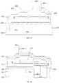
- FIG. 3A is a schematic partial sectional view of the bulk acoustic wave resonator along line O-A in FIG. 3 according to an exemplary embodiment of the present disclosure.
- the bulk acoustic wave resonator includes a substrate 200 and an acoustic mirror 210 provided on an upper surface of the substrate or embedded in an interior of the substrate.
- the acoustic mirror is formed by a cavity provided in the substrate, and any other acoustic mirror structures such as a Bragg reflector may be applicable.
- the bulk acoustic wave resonator further includes a bottom electrode 220, a piezoelectric layer 230, a top electrode 240, an insertion protruding structure 250, and an insertion wing structure 260. Further, the insertion protruding structure 250 and the insertion wing structure 260 form a composite insertion structure.
- the bottom electrode 220 is deposited on an upper surface of the acoustic mirror and covers the acoustic mirror.
- the bottom electrode 220 is etched into a bevel at an edge thereof, and the bevel is located outside the acoustic mirror. Alternatively, the edge of the bottom electrode 220 may be etched into a stepped shape, a vertical shape or other similar structures.
- the top electrode is located inside the acoustic mirror, and a distance d14 between the top electrode and the acoustic mirror is in a range of 0 to 10 um.
- the bottom electrode is located outside the acoustic mirror, a distance between a first end of the bottom electrode and the acoustic mirror is d13, and the distance d13 is in a range of 0 to 10 um.
- the insertion wing structure 250 has a first end located inside the effective region and a second end aligned with the edge of the effective region or extending beyond the effective region.
- the first end of the insertion wing structure 250 is spaced apart from a first end of the top electrode 240 by a distance d22, which is in a range of 0 to 10 um.
- the insertion wing structure has a height h1 in a range of 50 A to 5000 A.
- the insertion protrusion 260 has a first end and a second end.
- the first end of the insertion protrusion 260 is located inside the effective region.
- the first end of the insertion protrusion 260 is located closer to a center of the resonator than the first end of the insertion wing structure 250.
- the first end of the insertion protrusion 260 is spaced apart from the first end of the insertion wing structure 250 by a distance d21, which is in a range of 0 to 10 um.
- the second end of the insertion protrusion 260 may be located on the insertion wing structure 250 beyond an outer edge of the top electrode.
- the insertion protrusion 260 may cover the insertion wing structure and extend outwardly to a non-effective region.
- the bridge-wing layer is formed of air or made of a dielectric material.
- the bridge-wing layer may be the insertion bridge or the insertion wing, or the insertion bridge and the insertion wing.
- the bridge-wing layer is formed of air.
- the insertion protrusion may be located on the bridge-wing layer.
- the bridge-wing layer may be located above the insertion protrusion.
- FIG. 3B is a schematic partial sectional view of the bulk acoustic wave resonator along line O-B in FIG. 3 according to an exemplary embodiment of the present disclosure.
- the bottom electrode extends beyond the acoustic mirror, a distance between an edge of the bottom electrode and the acoustic mirror is defined as d25, and the distance d25 is in a range of 0 to 10 um.
- the insertion bridge structure 250 has a first end located inside the effective region and a second end located outside the bottom electrode, a distance between the second end of the insertion bridge structure 250 and an end of the bottom electrode is defined as d26, and the distance d26 is in a range of 0 to 10 um.
- the insertion protrusion 261 has a first end and a second end, and the first end of the insertion protrusion 261 is located closer to the center of the resonator than the first end of the insertion bridge 250.
- the first end of the insertion protrusion 261 is spaced apart from the first end of the insertion bridge structure by a distance d23, which is in a range of 0 to 10 um.
- the second end of the insertion protrusion 261 extends outwardly beyond the second end of the insertion bridge structure.
- the second end of the insertion protrusion 261 is spaced apart from the edge of the bottom electrode by a distance d27, which is in a range of 0 to 20 um.
- FIG. 3C is a schematic partial sectional view of the bulk acoustic wave resonator along line O-B in FIG. 3 according to another exemplary embodiment of the present disclosure.
- the embodiment shown in FIG. 3C is similar to that shown in FIG. 3B except that the second end of the insertion wing structure 260 is aligned with the second end of the insertion protrusion structure 250 rather than wrapping around the second end of the insertion protrusion structure 250 in FIG. 3C .
- the insertion wing structure in a sectional view parallel to the thickness direction of the resonator, may cover and surround the insertion protrusion structure or a part of the insertion protrusion structure.
- FIG. 3D illustrates a corresponding exemplary embodiment.
- FIG. 3D is a schematic partial sectional view of the bulk acoustic wave resonator along line O-B in FIG. 3 according to another exemplary embodiment of the present disclosure.
- the embodiment shown in FIG. 3D is similar to that shown in FIG. 3B except that in FIG. 3D , the second end of the insertion wing structure 260 is located at an inner side of the second end of the insertion protrusion structure 260, rather than wrapping around the second end of the insertion protrusion structure 250.
- FIG. 4A is a schematic partial sectional view of a bulk acoustic wave resonator along a line in a position similar to line O-A in FIG. 2 according to an exemplary embodiment of the present disclosure.
- the embodiment shown in FIG. 4A is similar to that shown in FIG. 2A except that at an outer side of the edge of the effective region, a portion of the piezoelectric layer 130 on the composite insertion layer (the insert protrusion 350 corresponding to the first insertion layer and the insert wing structure corresponding to the second layer) is etched, and the first end of the top electrode overlaps with the first end of the piezoelectric layer in the thickness direction.
- the insertion wing structure 360 has a height h2 and a width d12.
- a first end of the insertion protrusion 350 is laterally located closer to the center of the resonator than the insertion wing structure 360, and is spaced apart from a first end of the insertion wing structure 360 by a distance d11. Further, a second end of the insertion protrusion 350 may be aligned with a second end of the insertion wing structure 360 or extend outwardly to a non-effective region.
- the insertion wing structure is made of a dielectric material such as SiO 2 , Si 3 N 4 , ALN or doped AlN with a different doping concentration from that of the piezoelectric layer, or is formed of air.
- the insertion protrusion is made of a metal.
- the second insertion layer i.e., the insertion wing structure
- the first insertion layer i.e., the insertion protrusion
- an outer end of a portion of the piezoelectric layer below the first insertion layer is located at an outer side of an outer end of a portion of the piezoelectric layer above the first insertion layer in the radial direction.
- an outer end of the top electrode is aligned with the outer end of the portion of the piezoelectric layer above the first insertion layer.
- FIG. 4B is a schematic partial sectional view of a bulk acoustic wave resonator along a line in a position similar to line O-A in FIG. 2 according to an exemplary embodiment of the present disclosure.
- the embodiment shown in FIG. 4B is similar to that shown in FIG. 4A except for an annular insertion protrusion structure 361 and an annular insertion wing structure 351.
- the annular insertion wing structure 351 has a height h1 and a lateral distance d12, and is made of a dielectric material.
- a first end of the insertion protrusion structure 361 is located closer to the center of the resonator.
- the first end of the insertion protrusion structure 361 is spaced apart from a first end of the annular insertion wing structure 351 by a distance d11, and a second end of the insertion protruding structure 361 is at least connected to the insertion wing structure or extends outwardly, preferably parallel to the edge of the effective region.
- the insertion protrusion structure corresponding to the first insertion layer is located above the insertion wing structure corresponding to the second insertion layer.
- the first insertion layer covers and surrounds the second insertion layer or covers a part of the second insertion layer.
- the outer end of the portion of the piezoelectric layer below the first insertion layer is located at the outer side of the outer end of the portion of the piezoelectric layer above the first insertion layer in the radial direction.
- FIG. 5 is a performance comparison diagram of Rp values of structures as shown in FIGS. 2A , 4A and 1A .
- the insertion wing is formed of air, and has a height h2 of 1000 A and a width d12 of 1 um.
- the annular protrusion 150 is made of Mo (molybdenum) and has a height h1 of 1300 A.
- parallel resistances (Rp) of the two composite insertion structures both are significantly greater than that of the conventional composite structure.
- an average value of the parallel resistances Rp is significantly superior as compared with that of the entire piezoelectric layer.
- the effective length d11 of the annular protrusion is 1.5 um and 3 um
- the partial piezoelectric composite insertion structure has a maximum Rp which may be is high up to5800 ohms.
- the Rp value of the entire piezoelectric composite insertion structure is 5250A ohm.
- the Rp value of the conventional composite structure is 3700 ohms, and Rp values of parts of the piezoelectric composite insertion structure are greater than the entire piezoelectric composite insertion structure and the conventional composite structure by 56.8% and 10.5%, respectively.
- the second insertion layer when the second insertion layer is configured to be a wing, the second insertion layer has a wing structure.
- the second insertion layer when the second insertion layer is configured to be a bridge, the second insertion layer has a bridge structure.
- the resonator may include only the wing structure or the bridge structure, or may include both the bridge structure and the wing structure, as desired.
- the electrodes and the insertion protrusion may be made of gold (Au), tungsten (W), molybdenum (Mo), platinum (Pt), ruthenium (Ru), iridium (Ir), titanium tungsten (TiW), aluminum (Al), titanium (Ti), osmium (Os), magnesium (Mg), gold (Au), tungsten (W), molybdenum (Mo), platinum (Pt), ruthenium (Ru), iridium (Ir), germanium (Ge), copper (Cu), aluminum (Al), chromium (Cr), arsenic-doped gold and other similar metals.
- the passivation layer is made of a dielectric material
- the wing-bridge structure is also made of a dielectric material.
- the dielectric material may be selected from, but not limited to, one or more of silicon dioxide (SiO 2 ), silicon nitride (Si 3 N 4 ), silicon carbide (SiC), aluminum nitride (AlN), aluminum oxide (Al 2 O 3 ), porous silicon, fluorinated amorphous carbon, fluoropolymer, parylene, polyarylene ether, hydrogen silsesquioxane, cross-linked polyphenylene polymer, bisphenylcyclobutene, fluorinated silica, carbon-doped oxide and diamond, or a combination thereof.
- the piezoelectric layer may be made of aluminum nitride (AlN), doped aluminum nitride (doped ALN), zinc oxide (ZnO), lead zirconate titanate (PZT), lithium niobate (LiNbO 3 ), quartz, potassium niobate (KNbO 3 ) or lithium tantalate (LiTaO 3 ), and the like.
- the doped ALN contains at least one rare earth element, such as scandium (Sc), yttrium (Y), magnesium (Mg), titanium (Ti), lanthanum (La), cerium (Ce), praseodymium (Pr), neodymium (Nd), promethium (Pm), samarium (Sm), europium (Eu), gadolinium (Gd), terbium (Tb), dysprosium (Dy) , holmium (Ho), erbium (Er), thulium (Tm), ytterbium (Yb), and lutetium (Lu).
- rare earth element such as scandium (Sc), yttrium (Y), magnesium (Mg), titanium (Ti), lanthanum (La), cerium (Ce), praseodymium (Pr), neodymium (Nd), promethium (Pm), samarium (Sm), europium (Eu), gadolin
- the substrate is made of monocrystal silicon (Si), gallium arsenide (GaAs), sapphire, quartz or the like.
- the material of the substrate is not limited thereto.
Landscapes
- Physics & Mathematics (AREA)
- Acoustics & Sound (AREA)
- Engineering & Computer Science (AREA)
- Manufacturing & Machinery (AREA)
- Piezo-Electric Or Mechanical Vibrators, Or Delay Or Filter Circuits (AREA)
Abstract
Description
- Embodiments of the present disclosure relate to the field of semiconductors, and in particular, to a bulk acoustic wave resonator, a filter, and an electronic device having one of the bulk acoustic wave resonator and the filter.
- A bulk acoustic wave filter has been widely used in the current wireless communication systems due to its low insertion loss, high square coefficient, high power capacity and the like, and becomes an important component for determining quality of radio frequency signals received by or transmitted from the communication systems. Performance of the bulk acoustic wave filter is determined by a bulk acoustic wave resonator of the bulk acoustic wave filter. For example, a resonant frequency of the bulk acoustic wave resonator determines an operation frequency of the filter, an effective electromechanical coupling coefficient of the bulk acoustic wave resonator determines a bandwidth of the filter, and a quality factor of the bulk acoustic wave resonator determines insertion loss of the filter. When the filter has a predetermined structure, a quality factor thereof, especially the quality factor (or a series-parallel impedance) at a series resonant frequency and a parallel resonant frequency, will significantly affect a passband insertion loss. Therefore, it is important to improve the quality factor of the resonator when configuring the filter with high-performance. A quality factor (Qs) or series impedance (Rs) at the series resonant frequency of the bulk acoustic wave resonator is usually determined by electrode loss and material loss, and a quality factor (Qp) or parallel impedance (Rp) at the parallel resonant frequency of the bulk acoustic wave resonator is usually affected by boundary acoustic wave leakage. Therefore, when a material and an overlapping structure of the resonator are predetermined, improvement of Qs (or Rs) is limited. However, the boundary acoustic wave leakage may be effectively improved by changing a boundary structure of the resonator, thereby significantly improving the Qp (or Rp) of the resonator.
-
FIG. 1A is a schematic structural sectional view of a conventional film bulk acoustic wave resonator. As shown inFIG. 1 , areference sign 100 indicates a substrate, areference sign 110 indicates an acoustic mirror, areference sign 120 indicates a bottom electrode, areference sign 130 indicates a piezoelectric layer, areference sign 140 indicates a top electrode, areference sign 15 indicates an annular protruding structure, areference sign 16 indicates a wing structure, a reference sign h1 indicates a height of a gap, a reference sign h2 indicates a thickness of theprotruding structure 15, and areference sign 17 indicates a bridge structure. Reference signs d11-d14 indicate various dimensions. - As shown in
FIG. 1A , a composite structure is arranged at an edge of an effective region on an upper surface of the resonator. Accordingly, acoustic impedances on both sides of the edge of the effective region are not matched with each other, which limits propagation of transverse Lamb waves and enhances reflection and conversion capability to the Lamb waves, thereby improving the Rp. The piezoelectric layer has poor quality due to a rough edge of the bottom electrode at a connection side of the top electrode and the bottom electrode. The composite structure allows a resonance excitation caused by the piezoelectric layer with poor quality to contribute less to the entire circuit, and thus improves
-
FIG. 1B is a schematic structural sectional view of an existing film bulk acoustic wave resonator. As shown inFIG. 1B , areference sign 100 indicates a substrate, areference sign 110 indicates an acoustic mirror, areference sign 120 indicates a bottom electrode, areference sign 130 indicates a piezoelectric layer, areference sign 140 indicates a top electrode, areference sign 160 indicates an annular protruding structure, and a reference sign h2 indicates a thickness of the protruding structure. Reference signs d12 and d18 indicate various dimensions. - As shown in
FIG. 1B , theannular protrusion 160 is a single-layer structure which may be made of a metal or a dielectric material, or may be formed by air. In this arrangement, a single-layer insertion structure is arranged in the piezoelectric layer, and thus electrical properties of the resonator such as Rp can be improved. However, in the conventional composite structure or the single-layer insertion structure as described above, the energy leakage at the edge of the effective region of the resonator cannot be effectively improved, and the Rp thus cannot be effectively improved. - The present disclosure is provided to further improve an Rp value or a Qp value of a bulk acoustic wave resonator.
- According to an aspect of embodiments of the present disclosure, there is provided a bulk acoustic wave resonator. The bulk acoustic wave resonator is provided with a composite insertion structure arranged in the middle of a piezoelectric layer in an edge region of an effective region of the resonator. The composite insertion structure has an insertion protrusion corresponding to a first insertion layer and an insertion wing-bridge corresponding to a second insertion layer, thereby effectively increasing the Rp value of the bulk acoustic wave resonator. The bulk acoustic wave resonator includes a substrate, an acoustic mirror, a bottom electrode, a top electrode, and a piezoelectric layer. The acoustic mirror, the bottom electrode, the piezoelectric layer and the top electrode overlap with each other in a thickness direction of the substrate to form an overlapping region, and the overlapping region is an effective region of the resonator. The piezoelectric layer is provided with a composite insertion structure arranged along an edge of the effective region, and the composite insertion structure includes a first insertion layer and a second insertion layer. In a top view of the resonator, at least part of the first insertion layer overlaps with the effective region, and in the top view of the resonator, the first insertion layer at least partially overlaps with the second insertion layer. The first insertion layer is made of a metallic material and the second insertion layer is formed of air or made of a dielectric material, or the first insertion layer is made of a dielectric material and the second insertion layer is formed of air.
- Alternatively, at least part of the second insertion layer is arranged on the first insertion layer in a thickness direction of the resonator.
- Alternatively, in a sectional view parallel to the thickness direction of the resonator, the second insertion layer covers and surrounds the first insertion layer or covers a part of the first insertion layer. Further alternatively, in the sectional view parallel to the thickness direction of the resonator, an outer end of a portion of the piezoelectric layer below the first insertion layer is arranged at an outer side of an outer end of a portion of the piezoelectric layer above the first insertion layer in a radial direction. Furthermore, alternatively, an outer end of the top electrode is aligned with the outer end of the portion of the piezoelectric layer above the first insertion layer in the sectional view parallel to the thickness direction of the resonator.
- Alternatively, at least part of the first insertion layer is arranged on the second insertion layer in the thickness direction of the resonator. Further, alternatively, in a sectional view parallel to the thickness direction of the resonator, the first insertion layer covers and surrounds the second insertion layer or covers a part of the second insertion layer. Furthermore, alternatively, in the sectional view parallel to the thickness direction of the resonator, an outer end of a portion of the piezoelectric layer below the first insertion layer is arranged at an outer side of an outer end of a portion of the piezoelectric layer above the first insertion layer in a radial direction. Furthermore, alternatively, an outer end of the top electrode is aligned with the outer end of the portion of the piezoelectric layer above the first insertion layer and the outer end of the first insertion layer in the sectional view parallel to the thickness direction of the resonator.
- Alternatively, in a top view of the resonator, the second insertion layer, the first insertion layer and the effective region at least partially overlap with each other.
- Alternatively, the composite insertion structure is an annular insertion structure. Alternatively, the second insertion layer includes an insertion wing structure provided at a non-connection side of the electrodes in a top view of the resonator. Alternatively, the second insertion layer includes an insertion bridge structure provided at a connection side of the electrodes in a top view of the resonator. Further, a distance between an outer end of the insertion bridge structure and an end of the bottom electrode is in a range of 0 to 20 um in a radial direction. Furthermore, the first insertion layer extends beyond the bottom electrode, a distance between an outer end of the first insertion layer and the end of the bottom electrode is in a range of 0 to 10 um in the radial direction, and the distance between the outer end of the insertion bridge structure and the end of the bottom electrode in the radial direction is greater than the distance between the outer end of the first insertion layer and the end of the bottom electrode in the radial direction.
- Alternatively, in a top view of the resonator, at least part of the first insertion layer overlapping with the effective region is a flat insertion portion. Alternatively, the first insertion layer is a flat layer protrusion. Alternatively, the first insertion layer includes the flat insertion portion and a protrusion step portion, and the protrusion step portion and the flat insertion portion form a step; and/or the second insertion layer includes a wing-bridge step portion.
- Alternatively, at least part of the composite insertion structure is arranged at a middle position of a corresponding portion of the piezoelectric layer in a thickness direction of the piezoelectric layer.
- Alternatively, in a radial direction, a distance between an inner end of the first insertion layer and an inner end of the second insertion layer is in a range of 0 to 10 um. Further, the first insertion layer, the second insertion layer and the effective region overlap with each other in a range of 0 to 10 um in the thickness direction of the resonator.
- Alternatively, the first insertion layer has a thickness in a range of 50 A to 5000 A, and/or the second insertion layer has a thickness in a range of 50 A to 5000 A.
- Alternatively, the metal material includes at least one of gold (Au), tungsten (W), molybdenum (Mo), platinum (Pt), ruthenium (Ru), iridium (Ir), titanium tungsten (TiW), aluminum (Al), titanium (Ti), osmium (Os), magnesium (Mg), gold (Au), tungsten (W), molybdenum (Mo), platinum (Pt), puthenium (Ru), iridium (Ir), germanium (Ge), copper (Cu), aluminum (Al), chromium (Cr), or arsenic doped gold. The dielectric material includes at least one of silicon dioxide (SiO2), silicon nitride (Si3N4), silicon carbide (SiC), aluminum nitride (AlN), aluminum oxide (Al2O3), porous silicon, fluorinated amorphous carbon, fluoropolymer, parylene, polyarylene ether, hydrogen silsesquioxane, cross-linked polyphenylene polymer, bisphenylcyclobutene, fluorinated silica, carbon-doped oxide, or diamond.
- Alternatively, the first insertion layer and/or the second insertion layer span/spans a boundary of the effective region.
- Alternatively, the composite insertion structure is arranged between a first piezoelectric layer portion and a second piezoelectric layer portion, the first piezoelectric layer portion and the second piezoelectric layer portion form the piezoelectric layer, and a material of the first piezoelectric layer portion is different from a material of the second piezoelectric layer portion.
- According to another aspect of embodiments of the present disclosure, there is provided a filter including the bulk acoustic wave resonator as described above.
- According to a further aspect of embodiments of the present disclosure, there is provided an electronic device including the bulk acoustic wave resonator as described above or the filter as described above.
- The following description and drawings can facilitate to understand these and other features and advantages in various embodiments disclosed in the present disclosure. The same reference signs in the drawings always indicate the same components, wherein:
-
FIG. 1A is a schematic sectional view of a bulk acoustic wave resonator in the related art; -
FIG. 1B is a schematic sectional view of a bulk acoustic wave resonator in the related art; -
FIG. 2 is a schematic top view of a bulk acoustic wave resonator according to an exemplary embodiment of the present disclosure; -
FIG. 2A is a schematic partial sectional view of the bulk acoustic wave resonator along line O-A inFIG. 2 according to an exemplary embodiment of the present disclosure; -
FIG. 2B is a schematic view of a position arrangement of an insertion protrusion in a thickness direction of a piezoelectric layer according to an exemplary embodiment of the present disclosure; -
FIG. 2C is a schematic partial sectional view of the bulk acoustic wave resonator along line O-B inFIG. 2 according to an exemplary embodiment of the present disclosure; -
FIG. 2D is a schematic partial sectional view of the bulk acoustic wave resonator along line O-B inFIG. 2 according to another exemplary embodiment of the present disclosure; -
FIG. 2E is a schematic partial sectional view of the bulk acoustic wave resonator along line O-B inFIG. 2 according to a further another exemplary embodiment of the present disclosure; -
FIG. 2F is a schematic partial sectional view of the bulk acoustic wave resonator along line O-B inFIG. 2 according to a yet another exemplary embodiment of the present disclosure; -
FIG. 3 is a schematic top view of a bulk acoustic wave resonator according to an exemplary embodiment of the present disclosure; -
FIG. 3A is a schematic partial sectional view of the bulk acoustic wave resonator along line O-A inFIG. 3 according to an exemplary embodiment of the present disclosure; -
FIG. 3B is a schematic partial sectional view of the bulk acoustic wave resonator along line O-B inFIG. 3 according to an exemplary embodiment of the present disclosure; -
FIG. 3C is a schematic partial sectional view of the bulk acoustic wave resonator along line O-B inFIG. 3 according to another exemplary embodiment of the present disclosure; -
FIG. 3D is a schematic partial sectional view along line O-B inFIG. 3 according to another exemplary embodiment of the present disclosure; -
FIG. 4A is a schematic partial sectional view of a bulk acoustic wave resonator along a line in a position similar to line O-A inFIG. 2 according to an exemplary embodiment of the present disclosure; -
FIG. 4B is a schematic partial sectional view of a bulk acoustic wave resonator along a line in a position similar to line O-A inFIG. 2 according to an exemplary embodiment of the present disclosure; -
FIG. 5 is a comparison diagram of Rp values of structures shown inFIGS. 2A ,4A , and1A ; and -
FIG. 6 is a comparison diagram of Rp values of a single-layer metal insertion structure, a single-layer air insertion structure, and a double-layer insertion structure (including a metal layer and an air layer). - The technical solutions of the present disclosure will be further described below in detail through embodiments and in conjunction with the drawings. The same or similar reference signs indicate the same or similar components throughout the description. The following description of embodiments of the present disclosure with reference to the drawings is intended to explain the general inventive concept of the present disclosure, and should not be construed as a limitation to the present disclosure.
-
FIG. 2 is a schematic top view of a bulk acoustic wave resonator according to an exemplary embodiment of the present disclosure. As shown inFIG. 2 , the bulk acoustic wave resonator includes a bottom electrode, a piezoelectric layer, a top electrode, and a composite annular insertion structure. The top electrode may be covered with a passivation layer. The composite annular insertion structure is composed of an annular insertion protrusion structure and an annular insertion wing-bridge structure. The annular insertion wing-bridge structure is formed as an annular wing structure at a non-connection side of the bottom electrode and the top electrode, and formed as an annular bridge structure at a connection side of the top electrode and the bottom electrode. - In the present disclosure, for example, as shown in
FIG. 2 , the composite insertion structure has a serrated shape. However, an actual shape of the composite insertion structure is not necessarily in a serrated shape. The composite insertion structure may have an edge shape parallel to an edge of the top electrode. - It should be noted that, in the present disclosure, the insertion structure may be annular or not, which all falls within the scope of the present disclosure.
-
FIG. 2A is a schematic partial sectional view of the bulk acoustic wave resonator along line O-A inFIG. 2 according to an exemplary embodiment of the present disclosure. As shown inFIG. 2A , the bulk acoustic wave resonator includes asubstrate 100 and anacoustic mirror 110, which is located on an upper surface of the substrate or embedded in an interior thereof. As illustrated inFIG. 2A , the acoustic mirror is formed by a cavity embedded in the substrate, and any other acoustic mirror structures such as a Bragg reflector may also be applicable. The bulk acoustic wave resonator further includes abottom electrode 120, apiezoelectric layer 130, atop electrode 140, aninsertion protrusion 150, and aninsertion wing 160. Further, theinsertion protrusion 150 and theinsertion wing 160 form a composite insertion structure. Thetop electrode 140 may be provided with a passivation layer. Thebottom electrode 120 is deposited on an upper surface of the acoustic mirror and covers the acoustic mirror. Thebottom electrode 120 may be etched into a bevel at an edge thereof, and the bevel is located outside the acoustic mirror. Further, the edge of thebottom electrode 120 may be etched into a stepped or vertical shape or other similar structures. - The
acoustic mirror 110, thebottom electrode 120, thepiezoelectric layer 130 and thetop electrode 140 overlap with each other to form an overlapping region, which is an effective region of the resonator. The top electrode is located inside the acoustic mirror with a distance d14 in a range of 0 to 10 um from an edge of the acoustic mirror. The bottom electrode is located outside the acoustic mirror. A distance between a first end of the bottom electrode and the acoustic mirror is d13, and d13 is in a range of 0 to 10 um. - The
insertion protrusion 150 has a first end (an inner end) and a second end (an outer end). In embodiments of the present disclosure, for all components, a side close to a center of the effective region in a radial or lateral direction is defined as an inner side, and a side away from the center of the effective region in the radial or lateral direction is defined as an outer side. The first end of theinsertion protrusion 150 is located at the inner side of the effective region. The second end of theinsertion protrusion 150 is aligned with an edge of the effective region, or extends beyond the effective region by a distance d15 in a range of 0 to 20 um. The first end of theinsertion protrusion 150 is spaced apart from a first end of theinsertion wing 160 by a distance d11 in a range of 0 to 10 um. The insertion protrusion has a height h1 in a range of 50 A to 5000 A. - The
insertion wing 160 has the first end and a second end. The first end of theinsertion wing 160 is located on theinsertion protrusion 150 in a thickness direction, and is located between the edge of the effective region and the first end ofinsertion protrusion 150 in a horizontal direction. The second end of theinsertion wing 160 is aligned with the edge of the effective region or extends beyond the effective region. The second end of theinsertion wing 160 is spaced apart from the second end of theinsertion protrusion 150 by a distance d16 in a range of 0 to 20 um. The first end of theinsertion wing 160 is spaced apart from an edge of thetop electrode 140 by a distance d12 in a range of 0 to 10 um. Theinsertion wing 160 has a height h2 in a range of 50 A to 5000 A. - It should be specially noted that, in the present disclosure, for a numerical range, the numerical range may not only include end values of the numerical range, but also include a mean value or midpoint value within the numerical range.
- In this embodiment, the
insertion protrusion 150 is made of a metal, such as Mo, W, Cu, or Al. Theinsertion wing 160 is made of a dielectric material such as SiO2, Si3N4, ALN, doped AlN with a different doping concentration from the piezoelectric layer, or is formed of air. -
FIG. 2B is a schematic view of a position arrangement of the insertion protrusion in a thickness direction of the piezoelectric layer according to an exemplary embodiment of the present disclosure. More specifically, in the thickness direction of the resonator, the piezoelectric layer is divided equally into three parts by lines C-C and D-D. In addition, line E-E is defined as a horizontal central line of the insertion protrusion, and is located in the middle of contour lines shown by the lines C-C and D-D. InFIG. 2A , the insertion protrusion may be arranged such that the insertion protrusion and the insertion wing overlap with each other to form an overlapping portion. In addition, such the overlapping portion may be formed in the piezoelectric layer. - In the present disclosure, the insertion protrusion is arranged in the middle of the piezoelectric layer as long as the insertion protrusion is arranged between the lines C-C and D-D.
- In the embodiment as shown in
FIG. 2A , a composite insertion layer (an insertion protruding layer corresponding to a first insertion layer and a wing-bridge layer corresponding to a second insertion layer) provided in the piezoelectric layer is located at a position where a stress is maximum in a resonator piston mode, which corresponds to a special arrangement in which the composite insertion layer is located in the middle of the piezoelectric layer. Accordingly, the resulting impedance mismatch has a stronger reflection effect on the acoustic waves. Meanwhile, compared to a single insertion layer such as a single protruding layer, arranging two insertion layers in the piezoelectric layer can provide an impedance mismatch interface between the effective region and an non-effective region of the resonator, so that leakage waves propagating laterally are reflected multiple times, thereby increasing a Q value of the resonator, especially a Q value (or a parallel resonance impedance Rp) of the resonator at a parallel resonance frequency.FIG. 6 illustrates a simulation comparison result of an arrangement in which for example a metal insertion layer and an air insertion layer are provided according to an exemplary embodiment of the present disclosure versus an arrangement in which for example a single metal layer or a single air layer is provided. As can be seen fromFIG. 6 , the present disclosure achieves a higher Rp value than the existing single-layer insertion structure. -
FIG. 2C is a schematic partial sectional view of the bulk acoustic wave resonator along line O-B inFIG. 2 according to an exemplary embodiment of the present disclosure. InFIG. 2C , the bottom electrode extends beyond the acoustic mirror, and a distance d19 between an edge of the bottom electrode and the acoustic mirror is in a range of 0 to 10 um. Theinsertion protrusion 150 has a first end located inside the effective region and a second end aligned with the acoustic mirror. The first end of theinsertion protrusion 150 is spaced apart from a first end of aninsertion bridge 161 by a distance d17 in a range of 0 to 10 um. Theinsertion bridge 161 has the first end located on theinsertion protrusion 150 in the thickness direction and a second end. The first end of theinsertion bridge 161 is spaced apart from the edge of the acoustic mirror by a distance d18 in a range of 0 to 10 um. The second end of theinsertion bridge 161 extends beyond the bottom electrode, and a distance d20 between the bottom electrode and the second end of theinsertion bridge 161 is in a range of 0 to 20 um. -
FIG. 2D is a schematic partial sectional view of the bulk acoustic wave resonator along line O-B inFIG. 2 according to another exemplary embodiment of the present disclosure. The embodiment shown inFIG. 2D is similar to that shown inFIG. 2C except that the second end of theinsertion protrusion 150 extends beyond the effective region with an extension amount d1. -
FIG. 2E is a schematic partial sectional view of the bulk acoustic wave resonator along line O-B inFIG. 2 according to a yet another exemplary embodiment of the present disclosure. The embodiment shown inFIG. 2E is similar to that shown inFIG. 2C except that the second end of theinsertion protrusion structure 150 extends beyond the edge of the bottom electrode by an extension amount d24 in a range of 0 to 10 um. In this arrangement, the process tolerance is increased. -
FIG. 2F is a schematic partial sectional view of the bulk acoustic wave resonator along line O-B inFIG. 2 according to a still another exemplary embodiment of the present disclosure. The embodiment shown inFIG. 2F is similar to that inFIG. 2A except that the piezoelectric layer is made of two different piezoelectric materials or piezoelectric materials with different doping concentrations. In this embodiment, a firstpiezoelectric layer 130 is made of pure ALN, and a secondpiezoelectric layer 131 is made of doped ALN. -
FIG. 3 is a schematic top view of a bulk acoustic wave resonator according to an exemplary embodiment of the present disclosure. In the embodiment shown inFIG. 3 , the bulk acoustic wave resonator includes a bottom electrode, a piezoelectric layer, a top electrode, and a composite annular insertion structure. The composite annular insertion structure is composed of an annular insertion protrusion and an annular insertion wing-bridge structure. The annular insertion wing-bridge structure is formed as an annular wing structure at a non-connection side of the bottom electrode and the top electrode, and is formed as an annular bridge structure at a connection side of the top electrode and the bottom electrode. -
FIG. 3A is a schematic partial sectional view of the bulk acoustic wave resonator along line O-A inFIG. 3 according to an exemplary embodiment of the present disclosure. As shown inFIG. 3A , the bulk acoustic wave resonator includes asubstrate 200 and anacoustic mirror 210 provided on an upper surface of the substrate or embedded in an interior of the substrate. As illustrated inFIG. 3A , the acoustic mirror is formed by a cavity provided in the substrate, and any other acoustic mirror structures such as a Bragg reflector may be applicable. The bulk acoustic wave resonator further includes abottom electrode 220, apiezoelectric layer 230, atop electrode 240, aninsertion protruding structure 250, and aninsertion wing structure 260. Further, theinsertion protruding structure 250 and theinsertion wing structure 260 form a composite insertion structure. Thebottom electrode 220 is deposited on an upper surface of the acoustic mirror and covers the acoustic mirror. Thebottom electrode 220 is etched into a bevel at an edge thereof, and the bevel is located outside the acoustic mirror. Alternatively, the edge of thebottom electrode 220 may be etched into a stepped shape, a vertical shape or other similar structures. - The
acoustic mirror 210, thebottom electrode 220, thepiezoelectric layer 230 and thetop electrode 240 overlap with each other to form an overlapping region, which is an effective region of the resonator. The top electrode is located inside the acoustic mirror, and a distance d14 between the top electrode and the acoustic mirror is in a range of 0 to 10 um. The bottom electrode is located outside the acoustic mirror, a distance between a first end of the bottom electrode and the acoustic mirror is d13, and the distance d13 is in a range of 0 to 10 um. Theinsertion wing structure 250 has a first end located inside the effective region and a second end aligned with the edge of the effective region or extending beyond the effective region. The first end of theinsertion wing structure 250 is spaced apart from a first end of thetop electrode 240 by a distance d22, which is in a range of 0 to 10 um. The insertion wing structure has a height h1 in a range of 50 A to 5000 A. Theinsertion protrusion 260 has a first end and a second end. The first end of theinsertion protrusion 260 is located inside the effective region. The first end of theinsertion protrusion 260 is located closer to a center of the resonator than the first end of theinsertion wing structure 250. The first end of theinsertion protrusion 260 is spaced apart from the first end of theinsertion wing structure 250 by a distance d21, which is in a range of 0 to 10 um. The second end of theinsertion protrusion 260 may be located on theinsertion wing structure 250 beyond an outer edge of the top electrode. Alternatively, theinsertion protrusion 260 may cover the insertion wing structure and extend outwardly to a non-effective region. - In the present disclosure, when the insertion protrusion (layer) is made of a metal material, the bridge-wing layer is formed of air or made of a dielectric material. In this case, the bridge-wing layer may be the insertion bridge or the insertion wing, or the insertion bridge and the insertion wing. In the present disclosure, when the insertion protrusion is made of a dielectric material, the bridge-wing layer is formed of air.
- In addition, in the present disclosure, the insertion protrusion may be located on the bridge-wing layer. Alternatively, the bridge-wing layer may be located above the insertion protrusion.
-
FIG. 3B is a schematic partial sectional view of the bulk acoustic wave resonator along line O-B inFIG. 3 according to an exemplary embodiment of the present disclosure. In -
FIG. 3B , the bottom electrode extends beyond the acoustic mirror, a distance between an edge of the bottom electrode and the acoustic mirror is defined as d25, and the distance d25 is in a range of 0 to 10 um. Theinsertion bridge structure 250 has a first end located inside the effective region and a second end located outside the bottom electrode, a distance between the second end of theinsertion bridge structure 250 and an end of the bottom electrode is defined as d26, and the distance d26 is in a range of 0 to 10 um. Theinsertion protrusion 261 has a first end and a second end, and the first end of theinsertion protrusion 261 is located closer to the center of the resonator than the first end of theinsertion bridge 250. The first end of theinsertion protrusion 261 is spaced apart from the first end of the insertion bridge structure by a distance d23, which is in a range of 0 to 10 um. Preferably, the second end of theinsertion protrusion 261 extends outwardly beyond the second end of the insertion bridge structure. The second end of theinsertion protrusion 261 is spaced apart from the edge of the bottom electrode by a distance d27, which is in a range of 0 to 20 um. -
FIG. 3C is a schematic partial sectional view of the bulk acoustic wave resonator along line O-B inFIG. 3 according to another exemplary embodiment of the present disclosure. The embodiment shown inFIG. 3C is similar to that shown inFIG. 3B except that the second end of theinsertion wing structure 260 is aligned with the second end of theinsertion protrusion structure 250 rather than wrapping around the second end of theinsertion protrusion structure 250 inFIG. 3C . - In the present disclosure, in a sectional view parallel to the thickness direction of the resonator, the insertion wing structure may cover and surround the insertion protrusion structure or a part of the insertion protrusion structure.
FIG. 3D illustrates a corresponding exemplary embodiment.FIG. 3D is a schematic partial sectional view of the bulk acoustic wave resonator along line O-B inFIG. 3 according to another exemplary embodiment of the present disclosure. The embodiment shown inFIG. 3D is similar to that shown inFIG. 3B except that inFIG. 3D , the second end of theinsertion wing structure 260 is located at an inner side of the second end of theinsertion protrusion structure 260, rather than wrapping around the second end of theinsertion protrusion structure 250. -
FIG. 4A is a schematic partial sectional view of a bulk acoustic wave resonator along a line in a position similar to line O-A inFIG. 2 according to an exemplary embodiment of the present disclosure. The embodiment shown inFIG. 4A is similar to that shown inFIG. 2A except that at an outer side of the edge of the effective region, a portion of thepiezoelectric layer 130 on the composite insertion layer (theinsert protrusion 350 corresponding to the first insertion layer and the insert wing structure corresponding to the second layer) is etched, and the first end of the top electrode overlaps with the first end of the piezoelectric layer in the thickness direction. - As shown in
FIG. 4A , theinsertion wing structure 360 has a height h2 and a width d12. A first end of theinsertion protrusion 350 is laterally located closer to the center of the resonator than theinsertion wing structure 360, and is spaced apart from a first end of theinsertion wing structure 360 by a distance d11. Further, a second end of theinsertion protrusion 350 may be aligned with a second end of theinsertion wing structure 360 or extend outwardly to a non-effective region. - In the above exemplary embodiments, the insertion wing structure is made of a dielectric material such as SiO2, Si3N4, ALN or doped AlN with a different doping concentration from that of the piezoelectric layer, or is formed of air. The insertion protrusion is made of a metal.
- In other words, in a sectional view parallel to the thickness direction of the resonator as shown in
FIG. 4A , the second insertion layer (i.e., the insertion wing structure) covers and surrounds the first insertion layer (i.e., the insertion protrusion), or covers a part of the first insertion layer. Further, in a sectional view parallel to the thickness direction of the resonator, an outer end of a portion of the piezoelectric layer below the first insertion layer is located at an outer side of an outer end of a portion of the piezoelectric layer above the first insertion layer in the radial direction. Furthermore, in a sectional view parallel to the thickness direction of the resonator, an outer end of the top electrode is aligned with the outer end of the portion of the piezoelectric layer above the first insertion layer. -
FIG. 4B is a schematic partial sectional view of a bulk acoustic wave resonator along a line in a position similar to line O-A inFIG. 2 according to an exemplary embodiment of the present disclosure. The embodiment shown inFIG. 4B is similar to that shown inFIG. 4A except for an annularinsertion protrusion structure 361 and an annularinsertion wing structure 351. The annularinsertion wing structure 351 has a height h1 and a lateral distance d12, and is made of a dielectric material. A first end of theinsertion protrusion structure 361 is located closer to the center of the resonator. The first end of theinsertion protrusion structure 361 is spaced apart from a first end of the annularinsertion wing structure 351 by a distance d11, and a second end of theinsertion protruding structure 361 is at least connected to the insertion wing structure or extends outwardly, preferably parallel to the edge of the effective region. - In other words, in
FIG. 4B , in the thickness direction of the resonator, at least part of the insertion protrusion structure corresponding to the first insertion layer is located above the insertion wing structure corresponding to the second insertion layer. Further, in a sectional view parallel to the thickness direction of the resonator, the first insertion layer covers and surrounds the second insertion layer or covers a part of the second insertion layer. Furthermore, in a sectional view parallel to the thickness direction of the resonator, the outer end of the portion of the piezoelectric layer below the first insertion layer is located at the outer side of the outer end of the portion of the piezoelectric layer above the first insertion layer in the radial direction. -
FIG. 5 is a performance comparison diagram of Rp values of structures as shown inFIGS. 2A ,4A and1A . In this embodiment, the insertion wing is formed of air, and has a height h2 of 1000 A and a width d12 of 1 um. Theannular protrusion 150 is made of Mo (molybdenum) and has a height h1 of 1300 A. As shown inFIG. 5 , when an effective length d11 of the annular protrusion has been increased from 0.5 um to 3 um, parallel resistances (Rp) of the two composite insertion structures both are significantly greater than that of the conventional composite structure. In the embodiment in which the piezoelectric layer is partially etched in the two composite insertion structures, an average value of the parallel resistances Rp is significantly superior as compared with that of the entire piezoelectric layer. When the effective length d11 of the annular protrusion is 1.5 um and 3 um, the partial piezoelectric composite insertion structure has a maximum Rp which may be is high up to5800 ohms. When the effective length d11 of the annular protrusion is 1.5 um, the Rp value of the entire piezoelectric composite insertion structure is 5250A ohm. The Rp value of the conventional composite structure is 3700 ohms, and Rp values of parts of the piezoelectric composite insertion structure are greater than the entire piezoelectric composite insertion structure and the conventional composite structure by 56.8% and 10.5%, respectively. - In the above embodiments, when the second insertion layer is configured to be a wing, the second insertion layer has a wing structure. Alternatively, when the second insertion layer is configured to be a bridge, the second insertion layer has a bridge structure. Thus, the resonator may include only the wing structure or the bridge structure, or may include both the bridge structure and the wing structure, as desired.
- The materials of the components of the bulk acoustic wave resonator according to the present disclosure will be described briefly below.
- In the present disclosure, the electrodes and the insertion protrusion may be made of gold (Au), tungsten (W), molybdenum (Mo), platinum (Pt), ruthenium (Ru), iridium (Ir), titanium tungsten (TiW), aluminum (Al), titanium (Ti), osmium (Os), magnesium (Mg), gold (Au), tungsten (W), molybdenum (Mo), platinum (Pt), ruthenium (Ru), iridium (Ir), germanium (Ge), copper (Cu), aluminum (Al), chromium (Cr), arsenic-doped gold and other similar metals.
- In the present disclosure, the passivation layer is made of a dielectric material, and the wing-bridge structure is also made of a dielectric material. The dielectric material may be selected from, but not limited to, one or more of silicon dioxide (SiO2), silicon nitride (Si3N4), silicon carbide (SiC), aluminum nitride (AlN), aluminum oxide (Al2O3), porous silicon, fluorinated amorphous carbon, fluoropolymer, parylene, polyarylene ether, hydrogen silsesquioxane, cross-linked polyphenylene polymer, bisphenylcyclobutene, fluorinated silica, carbon-doped oxide and diamond, or a combination thereof.
- In the present disclosure, the piezoelectric layer may be made of aluminum nitride (AlN), doped aluminum nitride (doped ALN), zinc oxide (ZnO), lead zirconate titanate (PZT), lithium niobate (LiNbO3), quartz, potassium niobate (KNbO3) or lithium tantalate (LiTaO3), and the like. The doped ALN contains at least one rare earth element, such as scandium (Sc), yttrium (Y), magnesium (Mg), titanium (Ti), lanthanum (La), cerium (Ce), praseodymium (Pr), neodymium (Nd), promethium (Pm), samarium (Sm), europium (Eu), gadolinium (Gd), terbium (Tb), dysprosium (Dy) , holmium (Ho), erbium (Er), thulium (Tm), ytterbium (Yb), and lutetium (Lu).
- In the present disclosure, the substrate is made of monocrystal silicon (Si), gallium arsenide (GaAs), sapphire, quartz or the like. However, the material of the substrate is not limited thereto.
- In view of the above description, the following technical solutions are provided.
- 1. A bulk acoustic wave resonator includes:
- a substrate;
- an acoustic mirror;
- a bottom electrode;
- a top electrode; and
- a piezoelectric layer,
- wherein the acoustic mirror, the bottom electrode, the piezoelectric layer and the top electrode overlap with each other in a thickness direction of the substrate to form an overlapping region, which is an effective region of the resonator;
- wherein the piezoelectric layer is provided with a composite insertion structure arranged along an edge of the effective region, the composite insertion structure includes a first insertion layer and a second insertion layer, at least part of the first insertion layer overlaps with the effective region in a top view of the resonator, and the first insertion layer at least partially overlaps with the second insertion layer in the top view of the resonator; and
- wherein the first insertion layer is made of a metallic material and the second insertion layer is formed of air or made of a dielectric material, or the first insertion layer is made of a dielectric material and the second insertion layer is formed of air.
- Alternatively, in the top view of the resonator, the second insertion layer, the first insertion layer and the effective region at least partially overlap with each other.
- Alternatively, the first insertion layer and/or the second insertion layer span(s) a boundary of the effective region.
- 2. A filter includes the resonator as described above.
- 3. An electronic device incudes the resonator as described above or the filter as described above. It should be noted that the electronic device herein includes, but is not limited to, intermediate products such as radio frequency front-ends, filter and amplifier modules, and terminal products such as mobile phones, WIFI, and drones.
- Although the embodiments of the present disclosure have been shown and described, it should be understood for those skilled in the art that modifications may be made to these embodiments without departing from the principle and spirit of the present disclosure, and the scope thereof is defined by the appended claims and their equivalents.
Claims (27)
- A bulk acoustic wave resonator, comprising:a substrate;an acoustic mirror;a bottom electrode;a top electrode; anda piezoelectric layer,wherein the acoustic mirror, the bottom electrode, the piezoelectric layer and the top electrode overlap with each other in a thickness direction of the substrate to form an overlapping region, and the overlapping region is an effective region of the resonator;wherein the piezoelectric layer is provided with a composite insertion structure arranged along an edge of the effective region, the composite insertion structure comprises a first insertion layer and a second insertion layer, wherein in a top view of the resonator, at least part of the first insertion layer overlaps with the effective region, and in the top view of the resonator, the first insertion layer at least partially overlaps with the second insertion layer; andwherein the first insertion layer is made of a metallic material and the second insertion layer is formed of air or made of a dielectric material, or the first insertion layer is made of a dielectric material and the second insertion layer is formed of air.
- The resonator according to claim 1, characterized in that in a thickness direction of the resonator, at least part of the second insertion layer is arranged on the first insertion layer.
- The resonator according to claim 2, characterized in that in a sectional view parallel to the thickness direction of the resonator, the second insertion layer covers and surrounds the first insertion layer or covers a part of the first insertion layer.
- The resonator according to claim 3, characterized in that in the sectional view parallel to the thickness direction of the resonator, an outer end of a portion of the piezoelectric layer below the first insertion layer is arranged at an outer side of an outer end of a portion of the piezoelectric layer above the first insertion layer in a radial direction.
- The resonator according to claim 4, characterized in that in the sectional view parallel to the thickness direction of the resonator, an outer end of the top electrode is aligned with the outer end of the portion of the piezoelectric layer above the first insertion layer.
- The resonator according to claim 1, characterized in that in a thickness direction of the resonator, at least part of the first insertion layer is arranged on the second insertion layer.
- The resonator according to claim 6, characterized in that in a sectional view parallel to the thickness direction of the resonator, the first insertion layer covers and surrounds the second insertion layer or covers a part of the second insertion layer.
- The resonator according to claim 7, characterized in that in the sectional view parallel to the thickness direction of the resonator, an outer end of a portion of the piezoelectric layer below the first insertion layer is arranged at an outer side of an outer end of a portion of the piezoelectric layer above the first insertion layer in a radial direction.
- The resonator according to claim 8, characterized in that in the sectional view parallel to the thickness direction of the resonator, an outer end of the top electrode is aligned with an outer end of the first insertion layer and the outer end of the portion of the piezoelectric layer above the first insertion layer.
- The resonator according to claim 1, characterized in that in a top view of the resonator, the second insertion layer, the first insertion layer and the effective region at least partially overlap with each other.
- The resonator according to claim 1, characterized in that the composite insertion structure is an annular insertion structure.
- The resonator according to claim 11, characterized in that in a top view of the resonator, the second insertion layer comprises an insertion wing structure provided at a non-connection side of the electrodes.
- The resonator according to claim 11, characterized in that in a top view of the resonator, the second insertion layer comprises an insertion bridge structure provided at a connection side of the electrodes.
- The resonator according to claim 13, characterized in that a distance between an outer end of the insertion bridge structure and an end of the bottom electrode in a radial direction is in a range of 0 to 20 um.
- The resonator according to claim 14, characterized in that the first insertion layer extends beyond the bottom electrode, a distance between an outer end of the first insertion layer and the end of the bottom electrode in the radial direction is in a range of 0 to 10 um, and the distance between the outer end of the insertion bridge structure and the end of the bottom electrode in the radial direction is greater than the distance of the outer end of the first insertion layer and the end of the bottom electrode in the radial direction.
- The resonator according to claim 1, characterized in that in a top view of the resonator, at least part of a portion of the first insertion layer overlapping with the effective region is a flat insertion portion.
- The resonator according to claim 16, characterized in that the first insertion layer is a flat layer protrusion.
- The resonator according to claim 16, characterized in that the first insertion layer comprises the flat insertion portion and a protrusion step portion, and the protrusion step portion and the flat insertion portion form a step; and/or
the second insertion layer comprises a wing-bridge step portion. - The resonator according to claim 1, characterized in that in a thickness direction of the piezoelectric layer, at least part of the composite insertion structure is arranged at a middle position of a corresponding portion of the piezoelectric layer.
- The resonator according to any one of claims 1 to 19, characterized in that an inner end of the first insertion layer is spaced apart from an inner end of the second insertion layer by a distance in a radial direction, and the distance is in a range of 0 to 10 um.
- The resonator according to claim 20, characterized in that the first insertion layer, the second insertion layer and the effective region overlap with each other in a range of 0 to 10 um in the thickness direction of the resonator.
- The resonator according to any one of claims 1 to 20, characterized in that the first insertion layer has a thickness in a range of 50 A to 5000 A, and/or the second insertion layer has a thickness in a range of 50 A to 5000 A.
- The resonator according to any one of claims 1 to 22, characterized in that the metal material comprises at least one of gold (Au), tungsten (W), molybdenum (Mo), platinum (Pt), ruthenium (Ru), iridium (Ir), titanium tungsten (TiW) , aluminum (Al), titanium (Ti), osmium (Os), magnesium (Mg), gold (Au), tungsten (W), molybdenum (Mo), platinum (Pt), puthenium (Ru), iridium (Ir), germanium (Ge), copper (Cu), aluminum (Al), chromium (Cr), or arsenic doped gold; and
the dielectric material comprises at least one of silicon dioxide (SiO2), silicon nitride (Si3N4), silicon carbide (SiC), aluminum nitride (AlN), aluminum oxide (Al2O3), porous silicon, fluorinated amorphous carbon, fluoropolymer, parylene, polyarylene ether, hydrogen silsesquioxane, cross-linked polyphenylene polymer, bisphenylcyclobutene, fluorinated silica, carbon-doped oxide, or diamond. - The resonator according to claim 1, characterized in that the first insertion layer and/or the second insertion layer span/spans a boundary of the effective region.
- The resonator according to claim 1, characterized in that the composite insertion structure is arranged between a first piezoelectric layer portion and a second piezoelectric layer portion, the first piezoelectric layer portion and the second piezoelectric layer portion form the piezoelectric layer, and a material of the first piezoelectric layer portion is different from a material of the second piezoelectric layer portion.
- A filter, comprising the bulk acoustic wave resonator according to any one of claims 1 to 25.
- An electronic device, comprising the bulk acoustic wave resonator according to any one of claims 1 to 25 or the filter according to claim 27.
Applications Claiming Priority (2)
| Application Number | Priority Date | Filing Date | Title |
|---|---|---|---|
| CN201910823229.8A CN111010104A (en) | 2019-09-02 | 2019-09-02 | Bulk acoustic wave resonator having piezoelectric layer with insertion structure, filter, and electronic apparatus |
| PCT/CN2020/086562 WO2021042741A1 (en) | 2019-09-02 | 2020-04-24 | Bulk acoustic wave resonator with piezoelectric layer having insert structure, and filter and electronic device |
Publications (2)
| Publication Number | Publication Date |
|---|---|
| EP4027517A1 true EP4027517A1 (en) | 2022-07-13 |
| EP4027517A4 EP4027517A4 (en) | 2022-10-26 |
Family
ID=70111840
Family Applications (1)
| Application Number | Title | Priority Date | Filing Date |
|---|---|---|---|
| EP20859838.3A Pending EP4027517A4 (en) | 2019-09-02 | 2020-04-24 | BULKY ACOUSTIC WAVES RESONATOR WITH PIEZOELECTRIC LAYER HAVING AN INSERT STRUCTURE, AND FILTER AND ELECTRONIC DEVICE |
Country Status (3)
| Country | Link |
|---|---|
| EP (1) | EP4027517A4 (en) |
| CN (1) | CN111010104A (en) |
| WO (1) | WO2021042741A1 (en) |
Families Citing this family (13)
| Publication number | Priority date | Publication date | Assignee | Title |
|---|---|---|---|---|
| CN111010104A (en) * | 2019-09-02 | 2020-04-14 | 天津大学 | Bulk acoustic wave resonator having piezoelectric layer with insertion structure, filter, and electronic apparatus |
| CN112134542B (en) * | 2020-06-01 | 2022-07-12 | 诺思(天津)微系统有限责任公司 | Bulk acoustic wave resonator, bulk acoustic wave resonator assembly and manufacturing method, filter and electronic equipment |
| CN111585537B (en) * | 2020-06-05 | 2024-02-20 | 武汉衍熙微器件有限公司 | Resonator and filter |
| CN111917393B (en) * | 2020-06-22 | 2021-06-01 | 诺思(天津)微系统有限责任公司 | Bulk acoustic wave resonator and manufacturing method, bulk acoustic wave resonator assembly, filter and electronic equipment |
| CN111934640B (en) * | 2020-06-28 | 2021-06-01 | 诺思(天津)微系统有限责任公司 | Bulk acoustic wave resonators, filters and electronics with insertion layers to boost power |
| KR20220014194A (en) * | 2020-07-28 | 2022-02-04 | 삼성전기주식회사 | Bulk-acoustic wave resonator and method for fabricating the same |
| CN112087216B (en) * | 2020-08-03 | 2022-02-22 | 诺思(天津)微系统有限责任公司 | Bulk acoustic wave resonator with acoustic hole, assembly, filter and electronic device |
| CN114070232A (en) * | 2020-08-03 | 2022-02-18 | 诺思(天津)微系统有限责任公司 | Bulk acoustic wave resonator, filter and electronic device having electrode terminals close to each other |
| CN114079430B (en) * | 2020-08-12 | 2026-01-23 | 诺思(天津)微系统有限责任公司 | Bulk acoustic wave resonator with laminated bump structure, method for manufacturing the same, filter, and electronic device |
| CN114257204B (en) * | 2020-09-22 | 2026-01-13 | 诺思(天津)微系统有限责任公司 | Bulk acoustic wave resonator having acoustic resistive layer, assembly and manufacturing method thereof, filter, and electronic device |
| CN114257198A (en) * | 2020-09-22 | 2022-03-29 | 诺思(天津)微系统有限责任公司 | Bulk acoustic wave resonator having a void layer, assembly and method of manufacturing the same, filter and electronic apparatus |
| CN114389559A (en) * | 2020-10-21 | 2022-04-22 | 诺思(天津)微系统有限责任公司 | Bulk acoustic wave resonator, bulk acoustic wave resonator component, filter, and electronic device |
| CN117013979B (en) * | 2022-12-14 | 2024-06-04 | 北京芯溪半导体科技有限公司 | Bulk acoustic wave resonator, preparation method thereof, filter and electronic equipment |
Family Cites Families (18)
| Publication number | Priority date | Publication date | Assignee | Title |
|---|---|---|---|---|
| US7694397B2 (en) * | 2006-02-24 | 2010-04-13 | Avago Technologies Wireless Ip (Singapore) Pte. Ltd. | Method of manufacturing an acoustic mirror for piezoelectric resonator |
| JP4471001B2 (en) * | 2008-01-23 | 2010-06-02 | セイコーエプソン株式会社 | Semiconductor sensor and manufacturing method of semiconductor sensor |
| US8253513B2 (en) * | 2010-03-16 | 2012-08-28 | Hao Zhang | Temperature compensated thin film acoustic wave resonator |
| CN103684336B (en) * | 2012-08-31 | 2017-01-11 | 安华高科技通用Ip(新加坡)公司 | Resonator device with electrode comprising embedded type temperature compensation layer |
| JP6371518B2 (en) * | 2013-12-17 | 2018-08-08 | 太陽誘電株式会社 | Piezoelectric thin film resonator, method for manufacturing the same, filter, and duplexer |
| JP2015165659A (en) * | 2014-02-28 | 2015-09-17 | アバゴ・テクノロジーズ・ジェネラル・アイピー(シンガポール)プライベート・リミテッド | Acoustic resonator including aluminum scandium nitride and temperature compensation feature |
| US9621126B2 (en) * | 2014-10-22 | 2017-04-11 | Avago Technologies General Ip (Singapore) Pte. Ltd. | Bulk acoustic resonator device including temperature compensation structure comprising low acoustic impedance layer |
| JP6298796B2 (en) * | 2015-05-28 | 2018-03-20 | 太陽誘電株式会社 | Piezoelectric thin film resonator and manufacturing method thereof |
| CN105680813B (en) * | 2016-02-25 | 2018-12-07 | 锐迪科微电子(上海)有限公司 | A kind of thin film bulk acoustic wave resonator and its manufacturing method |
| CN107181472B (en) * | 2016-03-10 | 2020-11-03 | 中芯国际集成电路制造(上海)有限公司 | Film bulk acoustic resonator, semiconductor device and method of manufacturing the same |
| US10128813B2 (en) * | 2016-04-21 | 2018-11-13 | Avago Technologies International Sales Pte. Limited | Bulk acoustic wave (BAW) resonator structure |
| JP6556099B2 (en) * | 2016-06-16 | 2019-08-07 | 太陽誘電株式会社 | Piezoelectric thin film resonator, filter and multiplexer |
| US11228299B2 (en) * | 2017-02-02 | 2022-01-18 | Taiyo Yuden Co., Ltd. | Piezoelectric thin film resonator with insertion film, filter, and multiplexer |
| JP6903471B2 (en) * | 2017-04-07 | 2021-07-14 | 太陽誘電株式会社 | Piezoelectric thin film resonators, filters and multiplexers |
| US10756701B2 (en) * | 2017-08-17 | 2020-08-25 | Samsung Electro-Mechanics Co., Ltd. | Bulk acoustic wave resonator |
| JP6950658B2 (en) * | 2017-11-29 | 2021-10-13 | 株式会社村田製作所 | Elastic wave device |
| CN109831175B (en) * | 2018-12-26 | 2023-10-20 | 天津大学 | Film bulk acoustic resonator |
| CN111010104A (en) * | 2019-09-02 | 2020-04-14 | 天津大学 | Bulk acoustic wave resonator having piezoelectric layer with insertion structure, filter, and electronic apparatus |
-
2019
- 2019-09-02 CN CN201910823229.8A patent/CN111010104A/en active Pending
-
2020
- 2020-04-24 WO PCT/CN2020/086562 patent/WO2021042741A1/en not_active Ceased
- 2020-04-24 EP EP20859838.3A patent/EP4027517A4/en active Pending
Also Published As
| Publication number | Publication date |
|---|---|
| CN111010104A (en) | 2020-04-14 |
| WO2021042741A1 (en) | 2021-03-11 |
| EP4027517A4 (en) | 2022-10-26 |
Similar Documents
| Publication | Publication Date | Title |
|---|---|---|
| CN111313857B (en) | Bulk acoustic resonator provided with insertion structure and temperature compensation layer, filter and electronic device | |
| WO2021042741A1 (en) | Bulk acoustic wave resonator with piezoelectric layer having insert structure, and filter and electronic device | |
| US10727808B2 (en) | Bulk acoustic wave resonator comprising a ring | |
| CN111245400B (en) | Bulk acoustic wave resonator, filter and electronic device having bridge insertion structure | |
| US9401691B2 (en) | Acoustic resonator device with air-ring and temperature compensating layer | |
| US9634642B2 (en) | Acoustic resonator comprising vertically extended acoustic cavity | |
| EP4016841A1 (en) | Resonator having composite annular structure, filter and electronic device | |
| CN111355466B (en) | Bulk acoustic resonator with multi-beam eave gap, filter and electronic device | |
| CN110061712A (en) | Acoustic resonator, filter and electronic equipment including convex annular beam eaves structure | |
| CN111262540A (en) | Bulk acoustic wave resonator, method of manufacturing the same, filter, and electronic apparatus | |
| CN111193484A (en) | Bulk acoustic wave resonator with rough surface, filter, and electronic device | |
| EP4027519A1 (en) | Bulk acoustic wave resonator and manufacturing method therefor, filter and electronic device | |
| EP3905521A1 (en) | Resonator with extension structure at connection portion of top electrode, filter and electronic device | |
| CN111384911A (en) | Apparatus and method for tuning acoustic resonator performance based on beam eaves size | |
| WO2022135252A1 (en) | Bulk acoustic resonator having temperature compensation layer, and filter and electronic device | |
| CN114070231B (en) | Bulk acoustic wave resonator, filter and electronic device with temperature compensation layer | |
| CN114070232A (en) | Bulk acoustic wave resonator, filter and electronic device having electrode terminals close to each other | |
| CN115882812A (en) | Bulk acoustic wave resonator with raised structure angle selected to improve performance | |
| CN117526886A (en) | Bulk acoustic wave resonator with protrusions or depressions provided on the lower side of piezoelectric layer and manufacturing method | |
| CN112910433B (en) | Acoustic resonator for transverse excited shear mode | |
| US20250357910A1 (en) | Resonator and method for forming the same | |
| CN115765675A (en) | Bulk acoustic wave resonator, filter, and electronic device including gap electrode | |
| CN217037147U (en) | Acoustic resonator, filter comprising the same, and duplexer and multiplexer comprising the same | |
| CN114070238B (en) | Bulk acoustic wave resonator with temperature compensation layer, filter and electronic equipment | |
| CN111934640B (en) | Bulk acoustic wave resonators, filters and electronics with insertion layers to boost power |
Legal Events
| Date | Code | Title | Description |
|---|---|---|---|
| STAA | Information on the status of an ep patent application or granted ep patent |
Free format text: STATUS: THE INTERNATIONAL PUBLICATION HAS BEEN MADE |
|
| PUAI | Public reference made under article 153(3) epc to a published international application that has entered the european phase |
Free format text: ORIGINAL CODE: 0009012 |
|
| STAA | Information on the status of an ep patent application or granted ep patent |
Free format text: STATUS: REQUEST FOR EXAMINATION WAS MADE |
|
| 17P | Request for examination filed |
Effective date: 20220331 |
|
| AK | Designated contracting states |
Kind code of ref document: A1 Designated state(s): AL AT BE BG CH CY CZ DE DK EE ES FI FR GB GR HR HU IE IS IT LI LT LU LV MC MK MT NL NO PL PT RO RS SE SI SK SM TR |
|
| REG | Reference to a national code |
Ref country code: DE Ref legal event code: R079 Free format text: PREVIOUS MAIN CLASS: H03H0003020000 Ipc: H03H0009020000 |
|
| A4 | Supplementary search report drawn up and despatched |
Effective date: 20220923 |
|
| RIC1 | Information provided on ipc code assigned before grant |
Ipc: H03H 9/17 20060101ALI20220919BHEP Ipc: H03H 9/02 20060101AFI20220919BHEP |
|
| DAV | Request for validation of the european patent (deleted) | ||
| DAX | Request for extension of the european patent (deleted) | ||
| STAA | Information on the status of an ep patent application or granted ep patent |
Free format text: STATUS: EXAMINATION IS IN PROGRESS |
|
| 17Q | First examination report despatched |
Effective date: 20251107 |