EP4024383A1 - Display device and compensation method thereof - Google Patents
Display device and compensation method thereof Download PDFInfo
- Publication number
- EP4024383A1 EP4024383A1 EP21217752.1A EP21217752A EP4024383A1 EP 4024383 A1 EP4024383 A1 EP 4024383A1 EP 21217752 A EP21217752 A EP 21217752A EP 4024383 A1 EP4024383 A1 EP 4024383A1
- Authority
- EP
- European Patent Office
- Prior art keywords
- sensing
- period
- frame rate
- blank
- display device
- Prior art date
- Legal status (The legal status is an assumption and is not a legal conclusion. Google has not performed a legal analysis and makes no representation as to the accuracy of the status listed.)
- Pending
Links
Images





Classifications
-
- G—PHYSICS
- G09—EDUCATION; CRYPTOGRAPHY; DISPLAY; ADVERTISING; SEALS
- G09G—ARRANGEMENTS OR CIRCUITS FOR CONTROL OF INDICATING DEVICES USING STATIC MEANS TO PRESENT VARIABLE INFORMATION
- G09G3/00—Control arrangements or circuits, of interest only in connection with visual indicators other than cathode-ray tubes
- G09G3/20—Control arrangements or circuits, of interest only in connection with visual indicators other than cathode-ray tubes for presentation of an assembly of a number of characters, e.g. a page, by composing the assembly by combination of individual elements arranged in a matrix no fixed position being assigned to or needed to be assigned to the individual characters or partial characters
- G09G3/22—Control arrangements or circuits, of interest only in connection with visual indicators other than cathode-ray tubes for presentation of an assembly of a number of characters, e.g. a page, by composing the assembly by combination of individual elements arranged in a matrix no fixed position being assigned to or needed to be assigned to the individual characters or partial characters using controlled light sources
- G09G3/30—Control arrangements or circuits, of interest only in connection with visual indicators other than cathode-ray tubes for presentation of an assembly of a number of characters, e.g. a page, by composing the assembly by combination of individual elements arranged in a matrix no fixed position being assigned to or needed to be assigned to the individual characters or partial characters using controlled light sources using electroluminescent panels
- G09G3/32—Control arrangements or circuits, of interest only in connection with visual indicators other than cathode-ray tubes for presentation of an assembly of a number of characters, e.g. a page, by composing the assembly by combination of individual elements arranged in a matrix no fixed position being assigned to or needed to be assigned to the individual characters or partial characters using controlled light sources using electroluminescent panels semiconductive, e.g. using light-emitting diodes [LED]
- G09G3/3208—Control arrangements or circuits, of interest only in connection with visual indicators other than cathode-ray tubes for presentation of an assembly of a number of characters, e.g. a page, by composing the assembly by combination of individual elements arranged in a matrix no fixed position being assigned to or needed to be assigned to the individual characters or partial characters using controlled light sources using electroluminescent panels semiconductive, e.g. using light-emitting diodes [LED] organic, e.g. using organic light-emitting diodes [OLED]
- G09G3/3266—Details of drivers for scan electrodes
-
- G—PHYSICS
- G09—EDUCATION; CRYPTOGRAPHY; DISPLAY; ADVERTISING; SEALS
- G09G—ARRANGEMENTS OR CIRCUITS FOR CONTROL OF INDICATING DEVICES USING STATIC MEANS TO PRESENT VARIABLE INFORMATION
- G09G3/00—Control arrangements or circuits, of interest only in connection with visual indicators other than cathode-ray tubes
- G09G3/20—Control arrangements or circuits, of interest only in connection with visual indicators other than cathode-ray tubes for presentation of an assembly of a number of characters, e.g. a page, by composing the assembly by combination of individual elements arranged in a matrix no fixed position being assigned to or needed to be assigned to the individual characters or partial characters
- G09G3/22—Control arrangements or circuits, of interest only in connection with visual indicators other than cathode-ray tubes for presentation of an assembly of a number of characters, e.g. a page, by composing the assembly by combination of individual elements arranged in a matrix no fixed position being assigned to or needed to be assigned to the individual characters or partial characters using controlled light sources
- G09G3/30—Control arrangements or circuits, of interest only in connection with visual indicators other than cathode-ray tubes for presentation of an assembly of a number of characters, e.g. a page, by composing the assembly by combination of individual elements arranged in a matrix no fixed position being assigned to or needed to be assigned to the individual characters or partial characters using controlled light sources using electroluminescent panels
- G09G3/32—Control arrangements or circuits, of interest only in connection with visual indicators other than cathode-ray tubes for presentation of an assembly of a number of characters, e.g. a page, by composing the assembly by combination of individual elements arranged in a matrix no fixed position being assigned to or needed to be assigned to the individual characters or partial characters using controlled light sources using electroluminescent panels semiconductive, e.g. using light-emitting diodes [LED]
- G09G3/3208—Control arrangements or circuits, of interest only in connection with visual indicators other than cathode-ray tubes for presentation of an assembly of a number of characters, e.g. a page, by composing the assembly by combination of individual elements arranged in a matrix no fixed position being assigned to or needed to be assigned to the individual characters or partial characters using controlled light sources using electroluminescent panels semiconductive, e.g. using light-emitting diodes [LED] organic, e.g. using organic light-emitting diodes [OLED]
- G09G3/3225—Control arrangements or circuits, of interest only in connection with visual indicators other than cathode-ray tubes for presentation of an assembly of a number of characters, e.g. a page, by composing the assembly by combination of individual elements arranged in a matrix no fixed position being assigned to or needed to be assigned to the individual characters or partial characters using controlled light sources using electroluminescent panels semiconductive, e.g. using light-emitting diodes [LED] organic, e.g. using organic light-emitting diodes [OLED] using an active matrix
- G09G3/3233—Control arrangements or circuits, of interest only in connection with visual indicators other than cathode-ray tubes for presentation of an assembly of a number of characters, e.g. a page, by composing the assembly by combination of individual elements arranged in a matrix no fixed position being assigned to or needed to be assigned to the individual characters or partial characters using controlled light sources using electroluminescent panels semiconductive, e.g. using light-emitting diodes [LED] organic, e.g. using organic light-emitting diodes [OLED] using an active matrix with pixel circuitry controlling the current through the light-emitting element
-
- G—PHYSICS
- G09—EDUCATION; CRYPTOGRAPHY; DISPLAY; ADVERTISING; SEALS
- G09G—ARRANGEMENTS OR CIRCUITS FOR CONTROL OF INDICATING DEVICES USING STATIC MEANS TO PRESENT VARIABLE INFORMATION
- G09G3/00—Control arrangements or circuits, of interest only in connection with visual indicators other than cathode-ray tubes
- G09G3/20—Control arrangements or circuits, of interest only in connection with visual indicators other than cathode-ray tubes for presentation of an assembly of a number of characters, e.g. a page, by composing the assembly by combination of individual elements arranged in a matrix no fixed position being assigned to or needed to be assigned to the individual characters or partial characters
- G09G3/22—Control arrangements or circuits, of interest only in connection with visual indicators other than cathode-ray tubes for presentation of an assembly of a number of characters, e.g. a page, by composing the assembly by combination of individual elements arranged in a matrix no fixed position being assigned to or needed to be assigned to the individual characters or partial characters using controlled light sources
- G09G3/30—Control arrangements or circuits, of interest only in connection with visual indicators other than cathode-ray tubes for presentation of an assembly of a number of characters, e.g. a page, by composing the assembly by combination of individual elements arranged in a matrix no fixed position being assigned to or needed to be assigned to the individual characters or partial characters using controlled light sources using electroluminescent panels
- G09G3/32—Control arrangements or circuits, of interest only in connection with visual indicators other than cathode-ray tubes for presentation of an assembly of a number of characters, e.g. a page, by composing the assembly by combination of individual elements arranged in a matrix no fixed position being assigned to or needed to be assigned to the individual characters or partial characters using controlled light sources using electroluminescent panels semiconductive, e.g. using light-emitting diodes [LED]
- G09G3/3208—Control arrangements or circuits, of interest only in connection with visual indicators other than cathode-ray tubes for presentation of an assembly of a number of characters, e.g. a page, by composing the assembly by combination of individual elements arranged in a matrix no fixed position being assigned to or needed to be assigned to the individual characters or partial characters using controlled light sources using electroluminescent panels semiconductive, e.g. using light-emitting diodes [LED] organic, e.g. using organic light-emitting diodes [OLED]
-
- G—PHYSICS
- G09—EDUCATION; CRYPTOGRAPHY; DISPLAY; ADVERTISING; SEALS
- G09G—ARRANGEMENTS OR CIRCUITS FOR CONTROL OF INDICATING DEVICES USING STATIC MEANS TO PRESENT VARIABLE INFORMATION
- G09G3/00—Control arrangements or circuits, of interest only in connection with visual indicators other than cathode-ray tubes
- G09G3/20—Control arrangements or circuits, of interest only in connection with visual indicators other than cathode-ray tubes for presentation of an assembly of a number of characters, e.g. a page, by composing the assembly by combination of individual elements arranged in a matrix no fixed position being assigned to or needed to be assigned to the individual characters or partial characters
- G09G3/2007—Display of intermediate tones
- G09G3/2074—Display of intermediate tones using sub-pixels
-
- G—PHYSICS
- G09—EDUCATION; CRYPTOGRAPHY; DISPLAY; ADVERTISING; SEALS
- G09G—ARRANGEMENTS OR CIRCUITS FOR CONTROL OF INDICATING DEVICES USING STATIC MEANS TO PRESENT VARIABLE INFORMATION
- G09G3/00—Control arrangements or circuits, of interest only in connection with visual indicators other than cathode-ray tubes
- G09G3/20—Control arrangements or circuits, of interest only in connection with visual indicators other than cathode-ray tubes for presentation of an assembly of a number of characters, e.g. a page, by composing the assembly by combination of individual elements arranged in a matrix no fixed position being assigned to or needed to be assigned to the individual characters or partial characters
- G09G3/22—Control arrangements or circuits, of interest only in connection with visual indicators other than cathode-ray tubes for presentation of an assembly of a number of characters, e.g. a page, by composing the assembly by combination of individual elements arranged in a matrix no fixed position being assigned to or needed to be assigned to the individual characters or partial characters using controlled light sources
- G09G3/30—Control arrangements or circuits, of interest only in connection with visual indicators other than cathode-ray tubes for presentation of an assembly of a number of characters, e.g. a page, by composing the assembly by combination of individual elements arranged in a matrix no fixed position being assigned to or needed to be assigned to the individual characters or partial characters using controlled light sources using electroluminescent panels
- G09G3/32—Control arrangements or circuits, of interest only in connection with visual indicators other than cathode-ray tubes for presentation of an assembly of a number of characters, e.g. a page, by composing the assembly by combination of individual elements arranged in a matrix no fixed position being assigned to or needed to be assigned to the individual characters or partial characters using controlled light sources using electroluminescent panels semiconductive, e.g. using light-emitting diodes [LED]
- G09G3/3208—Control arrangements or circuits, of interest only in connection with visual indicators other than cathode-ray tubes for presentation of an assembly of a number of characters, e.g. a page, by composing the assembly by combination of individual elements arranged in a matrix no fixed position being assigned to or needed to be assigned to the individual characters or partial characters using controlled light sources using electroluminescent panels semiconductive, e.g. using light-emitting diodes [LED] organic, e.g. using organic light-emitting diodes [OLED]
- G09G3/3275—Details of drivers for data electrodes
-
- G—PHYSICS
- G09—EDUCATION; CRYPTOGRAPHY; DISPLAY; ADVERTISING; SEALS
- G09G—ARRANGEMENTS OR CIRCUITS FOR CONTROL OF INDICATING DEVICES USING STATIC MEANS TO PRESENT VARIABLE INFORMATION
- G09G3/00—Control arrangements or circuits, of interest only in connection with visual indicators other than cathode-ray tubes
- G09G3/20—Control arrangements or circuits, of interest only in connection with visual indicators other than cathode-ray tubes for presentation of an assembly of a number of characters, e.g. a page, by composing the assembly by combination of individual elements arranged in a matrix no fixed position being assigned to or needed to be assigned to the individual characters or partial characters
- G09G3/22—Control arrangements or circuits, of interest only in connection with visual indicators other than cathode-ray tubes for presentation of an assembly of a number of characters, e.g. a page, by composing the assembly by combination of individual elements arranged in a matrix no fixed position being assigned to or needed to be assigned to the individual characters or partial characters using controlled light sources
- G09G3/30—Control arrangements or circuits, of interest only in connection with visual indicators other than cathode-ray tubes for presentation of an assembly of a number of characters, e.g. a page, by composing the assembly by combination of individual elements arranged in a matrix no fixed position being assigned to or needed to be assigned to the individual characters or partial characters using controlled light sources using electroluminescent panels
- G09G3/32—Control arrangements or circuits, of interest only in connection with visual indicators other than cathode-ray tubes for presentation of an assembly of a number of characters, e.g. a page, by composing the assembly by combination of individual elements arranged in a matrix no fixed position being assigned to or needed to be assigned to the individual characters or partial characters using controlled light sources using electroluminescent panels semiconductive, e.g. using light-emitting diodes [LED]
- G09G3/3208—Control arrangements or circuits, of interest only in connection with visual indicators other than cathode-ray tubes for presentation of an assembly of a number of characters, e.g. a page, by composing the assembly by combination of individual elements arranged in a matrix no fixed position being assigned to or needed to be assigned to the individual characters or partial characters using controlled light sources using electroluminescent panels semiconductive, e.g. using light-emitting diodes [LED] organic, e.g. using organic light-emitting diodes [OLED]
- G09G3/3275—Details of drivers for data electrodes
- G09G3/3291—Details of drivers for data electrodes in which the data driver supplies a variable data voltage for setting the current through, or the voltage across, the light-emitting elements
-
- G—PHYSICS
- G09—EDUCATION; CRYPTOGRAPHY; DISPLAY; ADVERTISING; SEALS
- G09G—ARRANGEMENTS OR CIRCUITS FOR CONTROL OF INDICATING DEVICES USING STATIC MEANS TO PRESENT VARIABLE INFORMATION
- G09G2300/00—Aspects of the constitution of display devices
- G09G2300/04—Structural and physical details of display devices
- G09G2300/0421—Structural details of the set of electrodes
- G09G2300/043—Compensation electrodes or other additional electrodes in matrix displays related to distortions or compensation signals, e.g. for modifying TFT threshold voltage in column driver
-
- G—PHYSICS
- G09—EDUCATION; CRYPTOGRAPHY; DISPLAY; ADVERTISING; SEALS
- G09G—ARRANGEMENTS OR CIRCUITS FOR CONTROL OF INDICATING DEVICES USING STATIC MEANS TO PRESENT VARIABLE INFORMATION
- G09G2310/00—Command of the display device
- G09G2310/06—Details of flat display driving waveforms
- G09G2310/061—Details of flat display driving waveforms for resetting or blanking
-
- G—PHYSICS
- G09—EDUCATION; CRYPTOGRAPHY; DISPLAY; ADVERTISING; SEALS
- G09G—ARRANGEMENTS OR CIRCUITS FOR CONTROL OF INDICATING DEVICES USING STATIC MEANS TO PRESENT VARIABLE INFORMATION
- G09G2310/00—Command of the display device
- G09G2310/08—Details of timing specific for flat panels, other than clock recovery
-
- G—PHYSICS
- G09—EDUCATION; CRYPTOGRAPHY; DISPLAY; ADVERTISING; SEALS
- G09G—ARRANGEMENTS OR CIRCUITS FOR CONTROL OF INDICATING DEVICES USING STATIC MEANS TO PRESENT VARIABLE INFORMATION
- G09G2320/00—Control of display operating conditions
- G09G2320/02—Improving the quality of display appearance
- G09G2320/0233—Improving the luminance or brightness uniformity across the screen
-
- G—PHYSICS
- G09—EDUCATION; CRYPTOGRAPHY; DISPLAY; ADVERTISING; SEALS
- G09G—ARRANGEMENTS OR CIRCUITS FOR CONTROL OF INDICATING DEVICES USING STATIC MEANS TO PRESENT VARIABLE INFORMATION
- G09G2320/00—Control of display operating conditions
- G09G2320/02—Improving the quality of display appearance
- G09G2320/029—Improving the quality of display appearance by monitoring one or more pixels in the display panel, e.g. by monitoring a fixed reference pixel
- G09G2320/0295—Improving the quality of display appearance by monitoring one or more pixels in the display panel, e.g. by monitoring a fixed reference pixel by monitoring each display pixel
-
- G—PHYSICS
- G09—EDUCATION; CRYPTOGRAPHY; DISPLAY; ADVERTISING; SEALS
- G09G—ARRANGEMENTS OR CIRCUITS FOR CONTROL OF INDICATING DEVICES USING STATIC MEANS TO PRESENT VARIABLE INFORMATION
- G09G2320/00—Control of display operating conditions
- G09G2320/04—Maintaining the quality of display appearance
- G09G2320/041—Temperature compensation
-
- G—PHYSICS
- G09—EDUCATION; CRYPTOGRAPHY; DISPLAY; ADVERTISING; SEALS
- G09G—ARRANGEMENTS OR CIRCUITS FOR CONTROL OF INDICATING DEVICES USING STATIC MEANS TO PRESENT VARIABLE INFORMATION
- G09G2330/00—Aspects of power supply; Aspects of display protection and defect management
- G09G2330/04—Display protection
- G09G2330/045—Protection against panel overheating
-
- G—PHYSICS
- G09—EDUCATION; CRYPTOGRAPHY; DISPLAY; ADVERTISING; SEALS
- G09G—ARRANGEMENTS OR CIRCUITS FOR CONTROL OF INDICATING DEVICES USING STATIC MEANS TO PRESENT VARIABLE INFORMATION
- G09G2340/00—Aspects of display data processing
- G09G2340/04—Changes in size, position or resolution of an image
- G09G2340/0407—Resolution change, inclusive of the use of different resolutions for different screen areas
- G09G2340/0435—Change or adaptation of the frame rate of the video stream
Definitions
- the present disclosure relates to a display device and a compensation method thereof. More particularly, the present disclosure relates to a method of sensing a threshold voltage of a driving transistor of subpixels by changing a compensation time point in real-time when a display device is driven, and relates to a display device performing the method.
- LCD liquid crystal display
- PDP plasma display panel
- OLED organic light-emitting display
- An organic light-emitting element constituting the organic light-emitting display device is self-luminous and does not require a separate light source, so that the thickness and the weight of a display device may be reduced.
- the organic light-emitting display device has high quality characteristics, such as low power consumption, high luminance, and a high response rate.
- Such an organic light-emitting display device may have degradation in display quality due to the characteristics of transistors included within the organic light-emitting display device or due to the degradation of an organic light-emitting element.
- the present disclosure has been made keeping in mind the above problems occurring in the related art, and the present disclosure is intended to propose a method of sensing characteristics of a driving transistor of a subpixel and to propose a display device that is driven by the method.
- a display device including: a display panel including multiple subpixels; a gate driver configured to supply a scan signal during an active period of one frame to scan lines provided on the display panel, and configured to supply a sensing signal during a sensing period of a blank period of the one frame to sensing lines provided on the display panel; a data driver configured to supply a data voltage to data lines provided on the display panel; and a timing controller configured to control the gate driver and the data driver, wherein the timing controller may be further configured to determine a first active period, a first blank period, and a first sensing period when operating at a first frame rate, and to determine a second active period, a second blank period, and a second sensing period when operating at a second frame rate, wherein, when an operation is changed from the first frame rate to the second frame rate, the first sensing period and the second sensing period may be the same.
- the first frame rate may be greater than the second frame rate, and the first active period may be the same as the second active period.
- the second blank period may be longer than the first blank period.
- An ending time of the second sensing period may be the same as an ending time of the second blank period.
- a starting time of the second sensing period may be a time back-calculated as the second sensing period from an ending time of one frame at the second frame rate.
- the timing controller may select any one sensing line during the second blank period, and the gate driver may supply the sensing signal to the selected sensing line during the second sensing period.
- the timing controller may select multiple sensing lines during the second blank period, and the gate driver may supply the sensing signal to the selected multiple sensing lines during the second sensing period.
- the gate driver may be configured to sequentially supply the sensing signal to each of the multiple sensing lines.
- the multiple sensing lines may be adjacent to each other on the display panel in a pixel column direction.
- a compensation method of a display device including: determining an active period, a blank period, and a sensing period according to a frame rate; changing the frame rate from a first frame rate to a second frame rate; and sensing a subpixel during a second sensing period that is the same as a first sensing period.
- the first frame rate may be greater than the second frame rate, and a first active period may be the same as a second active period.
- a second blank period may be longer than a first blank period.
- An ending time of the second sensing period may be the same as an ending time of the second blank period.
- the sensing of the subpixel may include: starting the second sensing period at a time back-calculated as the second sensing period from an ending time of one frame at the second frame rate.
- the sensing of the subpixel may include: selecting any one sensing line during a second blank period when the frame rate is changed from the first frame rate to the second frame rate; and sensing the subpixel by supplying a sensing signal to the subpixel of the selected sensing line during the second sensing period.
- the sensing of the subpixel may include: selecting multiple sensing lines during a second blank period when the frame rate is changed from the first frame rate to the second frame rate; and sensing the subpixel by supplying a sensing signal to the subpixel of the selected multiple sensing lines during the second sensing period.
- the sensing by supplying the sensing signal may include: sensing the subpixel by sequentially supplying the sensing signal to each of the multiple sensing lines.
- the multiple sensing lines may be adjacent to each other on a display panel in a pixel column direction.
- an image quality of the display device may be improved.
- the memory allocation for a data reset may be reduced.
- FIG. 1 is a block diagram illustrating a configuration of a display device according to an embodiment of the present disclosure.
- a display device 1 includes a timing controller 10, a gate driver 20, a data driver 30, a power supply 40, and a display panel 50.
- the timing controller 10 may receive an image signal RGB and a control signal CS from outside.
- the image signal RGB may include a plurality of gray scale data.
- the control signal CS may include, for example, a horizontal synchronization signal, a vertical synchronization signal, and a main clock signal.
- the timing controller 10 may process the image signal RGB and the control signal CS to make the signals appropriate for an operation condition of the display panel 50, so that the timing controller 10 may output image data DATA, a gate driving control signal CONT1, a data driving control signal CONT2, and a power supply control signal CONT3.
- the gate driver 20 may be connected to pixels PX of the display panel 50 through multiple gate lines GL1 to GLn.
- the gate driver 20 may generate gate signals on the basis of the gate driving control signal CONT1 output from the timing controller 10.
- the gate driver 20 may provide the generated gate signals to the pixels PX through the multiple gate lines GL1 to GLn.
- the gate driver 20 may be further connected to the pixels PX of the display panel 50 through multiple second gate lines.
- the gate driver 20 may provide a sensing signal to the pixels PX through the multiple second gate lines.
- the sensing signal may be supplied so as to measure a characteristic of a driving transistor and/or a light-emitting element provided inside the pixels PX.
- the gate driver 20 may supply a scan signal during an active period of one frame to scan lines provided on the display panel 50, and supply a sensing signal during a sensing period of a blank period of the one frame to sensing lines provided on the display panel 50.
- the data driver 30 may be connected to the pixels PX of the display panel 50 through multiple data lines DL1 to DLm.
- the data driver 30 may generate data signals on the basis of the image data DATA and the data driving control signal CONT2 output from the timing controller 10.
- the data driver 30 may provide the generated data signals to the pixels PX through the multiple data lines DL1 to DLm.
- the data driver 30 may be further connected to the pixels PX of the display panel 50 through multiple sensing lines (or reference lines).
- the data driver 30 may provide a reference voltage (a sensing voltage, or an initialization voltage) to the pixels PX through the multiple sensing lines, or may sense states of the pixels PX on the basis of an electrical signal fed back from the pixels PX.
- the power supply 40 may be connected to the pixels PX of the display panel 50 through multiple power lines PL1 and PL2.
- the power supply 40 may generate a driving voltage to be provided to the display panel 50, on the basis of the power supply control signal CONT3.
- the driving voltage may include, for example, a high-potential driving voltage ELVDD and a low-potential driving voltage ELVSS.
- the power supply 40 may provide the generated driving voltages ELVDD and ELVSS to the pixels PX, through the corresponding power lines PL1 and PL2.
- pixels PX are disposed in the display panel 50.
- the pixels PX may be, for example, arranged in a matrix form on the display panel 50.
- Each pixel PX may be electrically connected to the corresponding gate line and the corresponding data line.
- the pixels PX may emit light with luminance corresponding to the gate signals and the data signals that are supplied through the gate lines GL1 to GLn and the data lines DL1 to DLm, respectively.
- Each pixel PX may display any one of a first to a third colors. For example, each pixel PX may also display any one of red, green, and blue colors. In another embodiment, each pixel PX may display any one of cyan, magenta, and yellow colors. In another embodiment, the pixels PX may be configured to display any one of four or more colors. For example, each pixel PX may also display any one of red, green, blue, and white colors.
- the timing controller 10, the gate driver 20, the data driver 30, and the power supply 40 may be configured as separate integrated circuits (ICs), or ICs in which at least some thereof are integrated.
- ICs integrated circuits
- at least one among the data driver 30 and the power supply 40 may be configured as an integrated circuit integrated with the timing controller 10.
- the gate driver 20 and the data driver 30 are illustrated as elements separated from the display panel 50, but at least one among the gate driver 20 and the data driver 30 may be configured in an in-panel manner that is formed integrally with the display panel 50.
- the gate driver 20 may be formed integrally with the display panel 50 according to a gate-in-panel (GIP) manner.
- GIP gate-in-panel
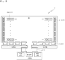
- FIG. 2 is a view illustrating the display device according to an embodiment of the present disclosure.
- the display panel 50 in a rectangular shape is illustrated, and the display panel 50 includes the multiple pixels PX arranged therein in the form of columns and rows.
- the multiple pixels PX may include four subpixels, and the four subpixels may be a red subpixel, R, a white subpixel, W, a green subpixel, G, and a blue subpixel, B, respectively.
- the display device 1 includes a gate driving IC (G-IC) 20.
- the display panel 50 may be implemented in a gate-in-panel (GIP) manner in which the gate driving IC 20 is disposed within the display panel 50.
- the gate driving IC 20 may be attached to a left side, a right side, or the left and right sides of the display panel 50.
- the display device 1 includes a data driving IC (source driving IC: S-IC) 30.
- the source driving IC 30 may be attached below the display panel 50, or multiple source driving ICs 30 may be attached in a transverse direction of the display panel 50.
- Such a source driving IC 30 may be implemented in a chip on film (COF) manner where it is disposed within a flexible PCB (FPCB), a chip on glass (COG) manner where it is disposed on a glass substrate constituting the display panel 50, and the like.
- COF chip on film
- FPCB flexible PCB
- COG chip on glass
- the source driving IC 30 is implemented in the COF manner, and the FPCB connects the display panel 50 and a source PCB (S-PCB) through pad connection.
- the source driving IC 30 may transmit a voltage (source IC driving voltage, EVDD, EVSS, VREF, etc.) provided to the display panel 50 from a control PCB (C-PCB).
- the source PCB may be connected to the display panel 50 from below the display panel 50 through the FPCB, and may be connected to the control PCB (C-PCB) through a flexible plat cable (FPC) connection.
- the source PCB (S-PCB) is directly connected to the source driving IC 30 and transmits the gate signal to the gate driving IC 20.
- the source PCB (S-PCB) receives power (ELVDD, ELVSS, VGH, VGL, VREF, etc.) from the control PCB (C-PCB) and transmits it to the display panel 50.
- a connection between the control PCB (C-PCB) and the gate driving IC 20 is provided through the leftmost or rightmost source driving IC 30 of the source PCB (S-PCB).
- a gate driving IC driving voltage, a gate high voltage VGH, a gate low voltage VGL, etc. are transmitted from the control PCB (C-PCB) to the gate driving IC 20 through the source PCB (S-PCB).
- the control PCB (C-PCB) is disposed below the display panel 50, and is connected to the display panel 50 through the source PCB (S-PCB) and the cable FPC.
- the control PCB (C-PCB) may include the timing controller (TCON) 10, the power supply (PMIC) 40, and a memory.
- TCON timing controller
- PMIC power supply
- the description of the timing controller 10 and the power supply 40 is the same as the description with reference to FIG. 1 .
- the control PCB (C-PCB) calculates an algorithm for every frame of an output image data to be output, stores compensation data, and requires an area for storing various parameters required for the algorithm calculation or various parameters for tuning. Accordingly, a volatile memory and/or a non-volatile memory may be disposed on the control PCB (C-PCB).
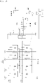
- FIG. 3 is a view illustrating a structure of a pixel according to an embodiment of the present disclosure.
- one pixel includes four subpixels R, W, G, and B, and each of the subpixels is connected to the gate driving IC (G-IC), a scan line SCAN, and a sensing line SENSE, and is connected to the source driving IC (S-IC) through a reference line REFERENCE.
- each subpixel receives a data voltage VDATA from the source driving IC (S-IC) through a digital analog converter DAC.
- a sensing voltage VSEN output from each subpixel is provided to the source driving IC (S-IC) through an analog digital converter ADC.
- each subpixel is connected to the high-potential driving voltage ELVDD and the low-potential driving voltage ELVSS.
- Each subpixel includes a scan TFT (S-TFT), a driving TFT (D-TFT), and a sensing TFT (SS-TFT).
- each subpixel includes a storage capacitor CST and a light-emitting element OLED.
- a first electrode (for example, a source electrode) of the scan transistor (S-TFT) is connected to the data line DL, and the data voltage VDATA is output from the source driving IC (S-IC) and is applied to the data line through the DAC.
- a second electrode (for example, a drain electrode) of the scan transistor (S-TFT) is connected to one end of the storage capacitor CST and is connected to a gate electrode of the driving TFT (D-TFT).
- the gate electrode of the scan transistor (S-TFT) is connected to the scan line (or the gate line GL). That is, the scan transistor (S-TFT) is turned on when the gate signal at a gate-on level is applied through the scan line SCAN, so that the data signal applied through the data line DL is transmitted to one end of the storage capacitor CST.
- One end of the storage capacitor CST is connected to a second electrode (for example, a drain electrode) of the scan TFT (S-TFT).
- the other end of the storage capacitor CST is configured to receive the high-potential driving voltage ELVDD.
- the storage capacitor CST may charge a voltage corresponding to a difference between a voltage applied to one end thereof and the high-potential driving voltage ELVDD applied to the other end thereof.
- the storage capacitor CST may charge a voltage corresponding to a difference between the voltage applied to one end thereof and a reference voltage VREF applied to the other end thereof through a switch SPRE and the sensing TFT (SS-TFT).
- a first electrode (For example, a source electrode) of the driving transistor (D-TFT) is configured to receive the high-potential driving voltage ELVDD, and a second electrode (for example, a drain electrode) is connected to a first electrode (for example, an anode electrode) of the light-emitting element OLED.
- a third electrode (for example, a gate electrode) of the driving transistor (D-TFT) is connected to one end of the storage capacitor CST.
- the driving transistor (D-TFT) is turned on when a voltage at the gate-on level is applied, and may control an amount of a driving current flowing through the light-emitting element OLED in response to a voltage provided to the gate electrode. That is, the current is determined by a voltage difference in the driving TFT (D-TFT) Vgs (or a storage voltage difference in the storage capacitor CST) and is applied to the light-emitting element OLED.
- a first electrode (for example, a source electrode) of the sensing TFT (SS-TFT) is connected to the reference line REFERENCE, and a second electrode (for example, a drain electrode) is connected to the other end of the storage capacitor CST.
- a third electrode (for example, a gate electrode) is connected to the sensing line SENSE. That is, the sensing TFT (SS-TFT) is turned on by a sensing signal output from the gate driving IC (G-IC) and applies the reference voltage VREF to the other end of the storage capacitor CST.
- the voltage VSEN stored in the reference line capacitor is output to the source driving IC (S-IC) through the ADC.
- This output voltage will be used as a voltage for sensing and sampling a degradation of a corresponding subpixel. That is, a voltage for compensating for a corresponding subpixel may be sensed and sampled.
- the characteristics of the driving TFT (D-TFT) are classified into two types of mobility and threshold voltage, and the compensation may be implemented by sensing the mobility and threshold voltage of the driving TFT (D-TFT).
- the characteristics of the corresponding subpixel may be also determined by the degradation of the light-emitting element OLED, and it is necessary to sense and compensate for the degree of degradation of the light-emitting element OLED.
- RT real-time compensation method
- the real-time compensation method is a method in which the mobility and the threshold voltage of the driving TFT (D-TFT) is compensated in real-time while the display device 1 is powered on and outputs the image data.
- the light-emitting element OLED outputs light corresponding to the driving current.
- the light-emitting element OLED may output light corresponding to any one of red, white, green, and blue colors.
- the light-emitting element OLED may be an organic light-emitting diode (OLED) or an ultra-small inorganic light-emitting diode having a size in a micro to nanoscale range, but the present disclosure is not limited thereto.
- OLED organic light-emitting diode
- ultra-small inorganic light-emitting diode having a size in a micro to nanoscale range
- FIG. 3 illustrates an example in which a scan transistor S-TFT, the driving transistor D-TFT, and the sensing transistor SS-TFT are NMOS transistors.
- the present disclosure is not limited thereto.
- at least some or all of the transistors constituting each pixel PX may be constructed as a PMOS transistor.
- each of the scan transistor S-TFT and the driving transistor D-TFT may be implemented as a low-temperature polycrystalline silicon (LTPS) thin-film transistor, an oxide thin-film transistor, or a low-temperature polycrystalline oxide (LTPO) thin-film transistor.
- LTPS low-temperature polycrystalline silicon
- LTPO low-temperature polycrystalline oxide
- each subpixel may be connected to one reference line REFERENCE.
- REFERENCE for convenience of description, as illustrated in FIG. 3 , it is described that four subpixels share one reference line REFERENCE, and it should be construed as an example.
- FIGS. 4 to 8 are views illustrating compensation for a mobility characteristic while the display device is driven. That is, the compensation in the present description is a compensation that is performed while the display device is powered on and the image data is being output. In addition, the compensation in the present description corresponds to a compensation for correcting a deviation by sensing the mobility characteristic of the driving TFT (D-TFT).
- D-TFT driving TFT
- the sensing of the mobility characteristic during the driving of the display device may be performed in a blank period between one frame and the next frame.
- the switch SPRE is turned on in an initialization period. Accordingly, the sensing voltage VSEN stored in the capacitor of the reference line is equal to the reference voltage VREF.
- the scan TFT (S-TFT) is turned on in a programming period.
- the data voltage VDATA is a high voltage. Accordingly, a charge corresponding to the data voltage VDATA is charged at one end of the storage capacitor CST.
- the sensing TFT (SS-TFT) is turned on and the switch SPRE is turned on. Accordingly, the other end of the storage capacitor CST is charged with a charge corresponding to the reference voltage VREF. That is, the voltage across the storage capacitor CST corresponds to a difference between the data voltage VDATA and the reference voltage VREF. Meanwhile, since the switch SPRE is maintained to be turned on, the sensing voltage VSEN is maintained as the reference voltage VREF.
- the scan TFT (S-TFT) is turned off and the sensing TFT (SS-TFT) is turned on.
- the driving TFT operates like a constant current source with a constant magnitude, and the current is applied to the reference line capacitor through the sensing TFT (SS-TFT). Accordingly, the sensing voltage VSEN increases with a constant voltage increase over time.
- the sensing TFT (SS-TFT) is turned off and another switch SAM is turned on. Accordingly, the sensing voltage VSEN is applied to the source driving IC (S-IC) via the ADC through the reference line REFERENCE.
- the source driving IC (S-IC) to which the sensing voltage VSEN is applied may calculate the mobility characteristic of the corresponding driving TFT.
- the scan TFT (S-TFT) is turned on, and the data voltage VDATA is a high voltage. That is, since the real-time compensation is performed, the process of FIGS. 4 to 8 is performed during the blank period between frame and frame. Therefore, a luminance deviation from another data line charged with an existing data voltage occurs. In order to correct the luminance deviation, the data of the previous frame is restored after the sampling period.
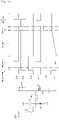
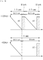
- FIG. 9 is a view illustrating one frame of both a high speed driving mode and a low speed driving mode.
- one frame period refers to a period in which one image is output.
- one image may be output through the display panel 50.
- a driving frequency 120 Hz
- 120 images may be output through the display panel 50.
- the driving frequency 60 Hz
- 60 images may be output through the display panel 50.
- a video image is displayed.
- a still image is displayed.
- the display device 1 may be driven in the high speed driving mode.
- the display device 1 may be driven in the low speed driving mode.
- the high speed driving mode and the low speed driving mode are described as the 120 Hz driving frequency and the 60 Hz driving frequency, respectively.
- a frame rate in the high speed driving mode is 120Hz, which is referred to as a first frame rate in the present specification.
- a frame rate in the low speed driving mode is 60 Hz, which is referred to as a second frame rate in the present specification.
- the embodiment is not limited thereto.
- one frame of the high speed driving mode and one frame of the low speed driving mode include an active period and a vertical blank period.
- a sensing period for sensing the mobility characteristic of the driving TFT may be performed within the blank period.
- the active period in the first frame rate (120 Hz), the active period may be determined as a first active period, the blank period may be determined as a first blank period, and the sensing period may be determined as a first sensing period.
- the active period in the second frame rate (60 Hz), the active period may be determined as a second active period, the blank period may be determined as a second blank period, and the sensing period may be determined as a second sensing period.
- the first active period in the 120 Hz is 8.33 milliseconds (ms)
- the first blank period is 300 microseconds ( ⁇ s)
- the first sensing period RT may be the same as the first blank period. Therefore, sum of a total of 120 frame periods may be 1 second.
- the second active period in the 60 Hz is 8.33 ms
- the second blank period is 8.33 ms +600 ⁇ s
- the second sensing period RT may be 300 ⁇ s that is the same as the first sensing period.
- the first active period and the second active period may be determined to be the same.
- the second blank period may be determined to be longer than the first blank period.
- the second blank period may be determined to be a sum of the first active period and two first blank periods.
- the second sensing period may be determined to be the same as the first sensing period.
- the first frame rate (120 Hz) may be greater than the second frame rate (60 Hz).
- the first active period, the first blank period, and the first sensing period may be determined.
- the 120 Hz driving that is the first frame rate one frame period includes one first active period and one first blank period, and the first sensing period may be included during the first blank period.
- the 60 Hz driving that is the second frame rate one frame period includes one second active period and one second blank period, and the second sensing period may be included during the second blank period. That is, two frames in driving at the first frame rate (120 Hz) may be one frame in driving at the second frame rate (60 Hz).
- the first sensing period and the second sensing period may be the same.
- the first active period may be the same as the second active period.
- the second blank period may be longer than the first blank period.
- an ending time of the second sensing period may be the same as an ending of the second blank period.
- the ending time of the second sensing period may be the same as an ending time of the frame at the second frame rate.
- a starting time of the second sensing period may be after an ending time of the second active period (the second blank period - the second sensing period).
- the starting time of the second sensing period may be a time back-calculated as the second sensing period from the ending time of one frame at the second frame rate.
- the first frame period, the first active period, the first blank period, the first sensing period, the second frame period, the second active period, the second blank period, and the second sensing period that are as described above may be stored as parameters in the memory of the display device according to the present disclosure.
- the display device may perform the driving according to the frame period, the active period, the blank period, and the sensing period that are depending on the frame rate determined by referencing the parameters.
- the gate driver 20 and the data driver 30 may sequentially scan the pixels PX according to a control of the timing controller 10, and the image data may be supplied to each subpixel.
- the gate driver 20 and the data driver 30 may select any one sensing line and may perform the real-time compensation.
- the gate driver 20 may supply the sensing signal to the selected sensing line during the second sensing period.
- a variable refresh rate (VRR) driving mode that outputs an image by changing the driving frequency may be used.
- the VRR driving mode refers to a driving manner of driving the display device 1.
- an image having a relatively large gray scale change is driven at the high speed driving mode of which the driving frequency is 120 Hz, and an image having a relatively small gray scale change is driven at the low speed driving mode of which the driving frequency is 60 Hz.
- the active period of one frame is the same in both of the driving modes.
- the blank period at the low speed driving mode may be longer than the blank period at the high speed driving mode.
- a deviation in recovery data may occur since the real-time compensation is performed at the beginning of the blank period.
- the recovery data may include an image data before the sensing and a compensation value to compensate for luminance relatively reduced by a real-time sensing operation.
- the compensation value of the recovery data may include a compensation value to compensate for a difference in charging time of the image data and a difference in charging time of the recovery data.
- the blank period of the low speed driving mode is longer than the blank period of the high speed driving mode. Therefore, the charging time of the recovery data in the low speed driving mode has no choice but to be longer than the charging time of the recovery data in the high speed driving mode. Accordingly, in the conventional display device, the memory allocation for resetting a lookup table and the like according to a frame rate change is necessary.
- a sensing time may be determined so that the lookup table and the like are not reset by the VRR mode driving.
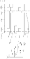
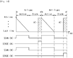
- FIG. 10 is a timing chart illustrating a real-time compensation method of the display device according to a first embodiment when a frame rate is changed from the high speed driving mode to the low speed driving mode.
- the gate driver 20 and the data driver 30 select any one sensing line (N or M) during the blank period of one frame and perform the real-time compensation for the selected sensing line during the sensing period, and may restore the previous image data display state for the sensing line on which the real-time compensation operation is performed during the data insertion period.
- the timing controller 10 may select any one sensing line during the second blank period.
- Each frame (N and N+1) in the low speed driving mode may include the active period and the blank period.
- the sensing period for sensing the mobility characteristic of the driving TFT may be performed within the blank period.
- the active period may refer to the second active period
- the blank period may refer to the second blank period
- the sensing period may refer to the second sensing period.
- the real-time compensation for an Nth sensing line may be performed during the second sensing period of the Nth frame, and the real-time compensation for an Mth sensing line may be performed during the second sensing period of the N+1th frame.
- an Mth line is positioned closest to an Nth line in a pixel column direction.
- the ending time of the second sensing period of the low speed driving mode may be determined to be the same as the ending time of the second blank period in order to reduce the deviation of recovery data between both the driving modes.
- both the scan TFT (S-TFT) and the sensing TFT (SS-TFT) are turned off at the initialization period in which the second blank period starts after the second active period.
- only the sensing TFT (SS-TFT) is turned on at the second sensing period of the second blank period before one frame period is ended. Accordingly, in the VRR driving mode, the recovery data at the high speed driving mode and the low speed driving mode are maintained to be the same, so that the resetting of the lookup table and the like becomes unnecessary.
- FIG. 11 is a timing chart illustrating the real-time compensation method of the display device according to a second embodiment when the frame rate is changed from the high speed driving mode to the low speed driving mode.
- the gate driver 20 and the data driver 30 may simultaneously select multiple sensing lines (N and M) during the blank period of the Nth frame, and may sequentially perform the real-time compensation for the selected sensing lines during the sensing period of the blank period.
- the timing controller 10 may select multiple sensing lines during the second blank period.
- the gate driver 20 may supply the sensing signal to the selected multiple sensing lines during the second sensing period. After performing the sensing operation, the previous image data display state may be restored for the multiple sensing lines (N and M) during the data insertion period.
- the Nth frame in the low speed driving mode may include the active period and the blank period.
- the sensing period for sensing the mobility characteristic of the driving TFT may be performed within the blank period.
- the active period may refer to the second active period
- the blank period may refer to the second blank period
- the sensing period may refer to the second sensing period.
- both the real-time compensation of the Nth sensing line and the real-time compensation of the Mth sensing line may be performed during the second blank period of the Nth frame.
- the Nth sensing line and the Mth sensing line may be disposed closest to each other in the pixel column direction on the display panel 50, or may be disposed at positions most spaced apart from each other in the pixel column direction.
- the ending time of the second sensing period of the low speed driving mode may be determined to be the same as the ending time of the second blank period in order to reduce the deviation of recovery data between the both driving modes.
- the Nth frame period in the low speed driving mode all of the scan TFT(S-TFT) and sensing TFT(SS-TFT) on the Nth line and the Mth line (corresponding to the scan signal SCAN (N), SCAN (M) and sensing signal SENSE (N), SENSE (M)) are turned off in the initialization period in which the second blank period starts after the second active period.
- the sensing TFT (SS-TFT) of the Nth sensing line and the sensing TFT (SS-TFT) of the Mth sensing line are sequentially turned on. That is, according to the second embodiment, by sequentially performing the real-time compensation of the Nth sensing line and the Mth sensing line within the second sensing period of the Nth frame period (i.e., by sequentially supplying the sensing signal to each of the the Nth sensing line and the Mth sensing line), the overall sensing time of the display panel 50 may be reduced.
- the present embodiment is not limited thereto.
- FIG. 12 is a flow chart illustrating the real-time compensation method when a driving mode of the display device according to an embodiment of the present disclosure is changed.
- the timing controller 10 may determine the frame rate as the high speed driving mode or the low speed driving mode, according to the image data output from the display panel 50.
- One frame period of each of the high speed driving mode and the low speed driving mode may include the active period and the vertical blank period.
- the sensing period for sensing the mobility characteristic of the driving TFT may be performed within the blank period.
- the active period in the first frame rate (120 Hz) that is the high speed driving mode, the active period may be determined as the first active period, the blank period may be determined as the first blank period, and the sensing period may be determined as the first sensing period.
- the active period in the second frame rate (60 Hz), the active period may be determined as the second active period, the blank period may be determined as the second blank period, and the sensing period may be determined as the second sensing period.
- the first active period in the 120 Hz is 8.33 ms
- the first blank period is 300 ⁇ s
- the first sensing period may be the same as the first blank period. Therefore, sum of a total of 120 frame periods may be 1 second.
- the second active period in the 60 Hz is 8.33 ms
- the second blank period is 8.33 ms +600 ⁇ s
- the second sensing period may be 300 ⁇ s that is the same as the first sensing period.
- the first active period and the second active period may be determined to be the same.
- the second blank period may be determined to be longer than the first blank period.
- the second blank period may be determined to be a sum of the first active period and two first blank periods.
- the second sensing period may be determined to be the same as the first sensing period.
- the gate driver 20 and the data driver 30 may sequentially scan the pixels PX and the image data may be supplied to each subpixel.
- the gate driver 20 and the data driver 30 may select any one sensing line and may perform the real-time compensation.
- the timing controller 10 may change the driving mode of the gate driver 20 and the data driver 30 from the high speed driving mode to the low speed driving mode. That is, the timing controller 10 may change the driving frequency so as to reduce the power consumption of the display device 1.
- the high speed driving mode and the low speed driving mode have the same active period of one frame, but the blank period of one frame in the low speed driving mode may be longer than the blank period of one frame in the high speed driving mode.
- the subpixel connected to the sensing line may be sensed during the sensing period in the low speed driving mode.
- the sensing period of the low speed driving mode may be maintained to be the same as the sensing period of the high speed driving mode. That is, the ending time of the sensing period of the low speed driving mode may be maintained to be the same as the ending time of the sensing period of the high speed driving mode. Further, in the low speed driving mode, the ending time of the sensing period may be the same as the ending time of the blank period.
Landscapes
- Engineering & Computer Science (AREA)
- Physics & Mathematics (AREA)
- Computer Hardware Design (AREA)
- General Physics & Mathematics (AREA)
- Theoretical Computer Science (AREA)
- Control Of Indicators Other Than Cathode Ray Tubes (AREA)
- Control Of El Displays (AREA)
- Electroluminescent Light Sources (AREA)
- Devices For Indicating Variable Information By Combining Individual Elements (AREA)
Abstract
Description
- The present application claims priority to
Korean Patent Application No. 10-2020-0189303, filed on December 31, 2020 - The present disclosure relates to a display device and a compensation method thereof. More particularly, the present disclosure relates to a method of sensing a threshold voltage of a driving transistor of subpixels by changing a compensation time point in real-time when a display device is driven, and relates to a display device performing the method.
- With the advancement of information-oriented society, various types of display devices have been developed. Recently, various display devices such as a liquid crystal display (LCD) device, a plasma display panel (PDP) display device, and an organic light-emitting display (OLED) device have been utilized.
- An organic light-emitting element constituting the organic light-emitting display device is self-luminous and does not require a separate light source, so that the thickness and the weight of a display device may be reduced. In addition, the organic light-emitting display device has high quality characteristics, such as low power consumption, high luminance, and a high response rate.
- Such an organic light-emitting display device may have degradation in display quality due to the characteristics of transistors included within the organic light-emitting display device or due to the degradation of an organic light-emitting element.
- Accordingly, the present disclosure has been made keeping in mind the above problems occurring in the related art, and the present disclosure is intended to propose a method of sensing characteristics of a driving transistor of a subpixel and to propose a display device that is driven by the method.
- According to an aspect, there is provided a display device including: a display panel including multiple subpixels; a gate driver configured to supply a scan signal during an active period of one frame to scan lines provided on the display panel, and configured to supply a sensing signal during a sensing period of a blank period of the one frame to sensing lines provided on the display panel; a data driver configured to supply a data voltage to data lines provided on the display panel; and a timing controller configured to control the gate driver and the data driver, wherein the timing controller may be further configured to determine a first active period, a first blank period, and a first sensing period when operating at a first frame rate, and to determine a second active period, a second blank period, and a second sensing period when operating at a second frame rate, wherein, when an operation is changed from the first frame rate to the second frame rate, the first sensing period and the second sensing period may be the same.
- The first frame rate may be greater than the second frame rate, and the first active period may be the same as the second active period.
- The second blank period may be longer than the first blank period.
- An ending time of the second sensing period may be the same as an ending time of the second blank period.
- A starting time of the second sensing period may be a time back-calculated as the second sensing period from an ending time of one frame at the second frame rate. When the operation is changed from the first frame rate to the second frame rate, the timing controller may select any one sensing line during the second blank period, and the gate driver may supply the sensing signal to the selected sensing line during the second sensing period.
- When the operation is changed from the first frame rate to the second frame rate, the timing controller may select multiple sensing lines during the second blank period, and the gate driver may supply the sensing signal to the selected multiple sensing lines during the second sensing period.
- The gate driver may be configured to sequentially supply the sensing signal to each of the multiple sensing lines. The multiple sensing lines may be adjacent to each other on the display panel in a pixel column direction.
- According to a second aspect, there is provided a compensation method of a display device, the compensation method including: determining an active period, a blank period, and a sensing period according to a frame rate; changing the frame rate from a first frame rate to a second frame rate; and sensing a subpixel during a second sensing period that is the same as a first sensing period.
- The first frame rate may be greater than the second frame rate, and a first active period may be the same as a second active period.
- A second blank period may be longer than a first blank period.
- An ending time of the second sensing period may be the same as an ending time of the second blank period.
- The sensing of the subpixel may include: starting the second sensing period at a time back-calculated as the second sensing period from an ending time of one frame at the second frame rate.
- The sensing of the subpixel may include: selecting any one sensing line during a second blank period when the frame rate is changed from the first frame rate to the second frame rate; and sensing the subpixel by supplying a sensing signal to the subpixel of the selected sensing line during the second sensing period.
- The sensing of the subpixel may include: selecting multiple sensing lines during a second blank period when the frame rate is changed from the first frame rate to the second frame rate; and sensing the subpixel by supplying a sensing signal to the subpixel of the selected multiple sensing lines during the second sensing period.
- The sensing by supplying the sensing signal may include: sensing the subpixel by sequentially supplying the sensing signal to each of the multiple sensing lines.
- The multiple sensing lines may be adjacent to each other on a display panel in a pixel column direction.
- According to the present disclosure, by sensing and compensating characteristic values of the driving transistor disposed on each subpixel, an image quality of the display device may be improved.
- In addition, according to the present disclosure, by changing a real-time compensation time of the display device when a variable refresh rate (VRR) driving mode is driven, the memory allocation for a data reset may be reduced.
- The above and other objectives, features, and other advantages of the present disclosure will be more clearly understood from the following detailed description when taken in conjunction with the accompanying drawings, in which:
-
FIG. 1 is a block diagram illustrating a configuration of a display device according to an embodiment of the present disclosure; -
FIG. 2 is a view illustrating the display device according to an embodiment of the present disclosure; -
FIG. 3 is a view illustrating a structure of a pixel according to an embodiment of the present disclosure; -
FIGS. 4 to 8 are views illustrating compensation for a mobility characteristic while the display device is driven; -
FIG. 9 is a view illustrating one frame of both a high speed driving mode and a low speed driving mode; -
FIG. 10 is a timing chart illustrating a real-time compensation method of the display device according to a first embodiment when a frame rate is changed from the high speed driving mode to the low speed driving mode; -
FIG. 11 is a timing chart illustrating the real-time compensation method of the display device according to a second embodiment when the frame rate is changed from the high speed driving mode to the low speed driving mode; and -
FIG. 12 is a flow chart illustrating the real-time compensation method when a driving mode of the display device according to an embodiment of the present disclosure is changed. - Hereinafter, embodiments of the present disclosure will be described in detail with reference to the accompanying drawings. In this specification, it will be understood that when one component (or region, layer, portion) is referred to as being "on", "connected to", or "coupled to" another component, it can be directly disposed/connected/coupled on/to the one component, or an intervening third component may also be present.
- Like reference numerals refer to like elements throughout. Also, in the drawings, the thickness, ratio, and dimensions of components are exaggerated for clarity of illustration. The term "and/or" includes one or more combinations that the associated elements may define.
- It will be understood that although the terms such as "first" and "second" are used herein to describe various elements, these elements should not be limited by these terms. The terms are only used to distinguish one component from other components. For example, an element referred to as a first element in one embodiment can be referred to as a second element in another embodiment without departing from the scope of the appended claims. The terms of a singular form may include plural forms unless referred to the contrary.
- Also, "under", "below", "above", "upper", and the like are used for explaining relation association of components illustrated in the drawings. These terms are relative concepts and are described on the basis of the direction in the drawings.
- The meaning of the term "include" or "comprise" specifies presence of a property, a fixed number, a step, an operation, an element, a component or a combination thereof, but does not exclude presence or addition of other properties, fixed numbers, steps, operations, elements, components or combinations thereof.
-
FIG. 1 is a block diagram illustrating a configuration of a display device according to an embodiment of the present disclosure. - Referring to
FIG. 1 , adisplay device 1 includes atiming controller 10, agate driver 20, adata driver 30, apower supply 40, and adisplay panel 50. - The
timing controller 10 may receive an image signal RGB and a control signal CS from outside. The image signal RGB may include a plurality of gray scale data. The control signal CS may include, for example, a horizontal synchronization signal, a vertical synchronization signal, and a main clock signal. - The
timing controller 10 may process the image signal RGB and the control signal CS to make the signals appropriate for an operation condition of thedisplay panel 50, so that thetiming controller 10 may output image data DATA, a gate driving control signal CONT1, a data driving control signal CONT2, and a power supply control signal CONT3. - The
gate driver 20 may be connected to pixels PX of thedisplay panel 50 through multiple gate lines GL1 to GLn. Thegate driver 20 may generate gate signals on the basis of the gate driving control signal CONT1 output from thetiming controller 10. Thegate driver 20 may provide the generated gate signals to the pixels PX through the multiple gate lines GL1 to GLn. - In various embodiments, the
gate driver 20 may be further connected to the pixels PX of thedisplay panel 50 through multiple second gate lines. Thegate driver 20 may provide a sensing signal to the pixels PX through the multiple second gate lines. The sensing signal may be supplied so as to measure a characteristic of a driving transistor and/or a light-emitting element provided inside the pixels PX. In one example, thegate driver 20 may supply a scan signal during an active period of one frame to scan lines provided on thedisplay panel 50, and supply a sensing signal during a sensing period of a blank period of the one frame to sensing lines provided on thedisplay panel 50. - The
data driver 30 may be connected to the pixels PX of thedisplay panel 50 through multiple data lines DL1 to DLm. Thedata driver 30 may generate data signals on the basis of the image data DATA and the data driving control signal CONT2 output from thetiming controller 10. Thedata driver 30 may provide the generated data signals to the pixels PX through the multiple data lines DL1 to DLm. - In various embodiments, the
data driver 30 may be further connected to the pixels PX of thedisplay panel 50 through multiple sensing lines (or reference lines). Thedata driver 30 may provide a reference voltage (a sensing voltage, or an initialization voltage) to the pixels PX through the multiple sensing lines, or may sense states of the pixels PX on the basis of an electrical signal fed back from the pixels PX. - The
power supply 40 may be connected to the pixels PX of thedisplay panel 50 through multiple power lines PL1 and PL2. Thepower supply 40 may generate a driving voltage to be provided to thedisplay panel 50, on the basis of the power supply control signal CONT3. The driving voltage may include, for example, a high-potential driving voltage ELVDD and a low-potential driving voltage ELVSS. Thepower supply 40 may provide the generated driving voltages ELVDD and ELVSS to the pixels PX, through the corresponding power lines PL1 and PL2. - In the
display panel 50, multiple pixels PX are disposed. The pixels PX may be, for example, arranged in a matrix form on thedisplay panel 50. - Each pixel PX may be electrically connected to the corresponding gate line and the corresponding data line. The pixels PX may emit light with luminance corresponding to the gate signals and the data signals that are supplied through the gate lines GL1 to GLn and the data lines DL1 to DLm, respectively.
- Each pixel PX may display any one of a first to a third colors. For example, each pixel PX may also display any one of red, green, and blue colors. In another embodiment, each pixel PX may display any one of cyan, magenta, and yellow colors. In another embodiment, the pixels PX may be configured to display any one of four or more colors. For example, each pixel PX may also display any one of red, green, blue, and white colors.
- The
timing controller 10, thegate driver 20, thedata driver 30, and thepower supply 40 may be configured as separate integrated circuits (ICs), or ICs in which at least some thereof are integrated. For example, at least one among thedata driver 30 and thepower supply 40 may be configured as an integrated circuit integrated with thetiming controller 10. - In addition, in
FIG. 1 , thegate driver 20 and thedata driver 30 are illustrated as elements separated from thedisplay panel 50, but at least one among thegate driver 20 and thedata driver 30 may be configured in an in-panel manner that is formed integrally with thedisplay panel 50. For example, thegate driver 20 may be formed integrally with thedisplay panel 50 according to a gate-in-panel (GIP) manner. -
FIG. 2 is a view illustrating the display device according to an embodiment of the present disclosure. - Referring to
FIG. 2 , thedisplay panel 50 in a rectangular shape is illustrated, and thedisplay panel 50 includes the multiple pixels PX arranged therein in the form of columns and rows. For example, the multiple pixels PX may include four subpixels, and the four subpixels may be a red subpixel, R, a white subpixel, W, a green subpixel, G, and a blue subpixel, B, respectively. - In addition, the
display device 1 includes a gate driving IC (G-IC) 20. Thedisplay panel 50 may be implemented in a gate-in-panel (GIP) manner in which thegate driving IC 20 is disposed within thedisplay panel 50. Thegate driving IC 20 may be attached to a left side, a right side, or the left and right sides of thedisplay panel 50. - In addition, the
display device 1 includes a data driving IC (source driving IC: S-IC) 30. Thesource driving IC 30 may be attached below thedisplay panel 50, or multiplesource driving ICs 30 may be attached in a transverse direction of thedisplay panel 50. Such asource driving IC 30 may be implemented in a chip on film (COF) manner where it is disposed within a flexible PCB (FPCB), a chip on glass (COG) manner where it is disposed on a glass substrate constituting thedisplay panel 50, and the like. - For example, in the embodiment illustrated in
FIG. 2 , thesource driving IC 30 is implemented in the COF manner, and the FPCB connects thedisplay panel 50 and a source PCB (S-PCB) through pad connection. Thesource driving IC 30 may transmit a voltage (source IC driving voltage, EVDD, EVSS, VREF, etc.) provided to thedisplay panel 50 from a control PCB (C-PCB). - The source PCB (S-PCB) may be connected to the
display panel 50 from below thedisplay panel 50 through the FPCB, and may be connected to the control PCB (C-PCB) through a flexible plat cable (FPC) connection. The source PCB (S-PCB) is directly connected to thesource driving IC 30 and transmits the gate signal to thegate driving IC 20. In addition, the source PCB (S-PCB) receives power (ELVDD, ELVSS, VGH, VGL, VREF, etc.) from the control PCB (C-PCB) and transmits it to thedisplay panel 50. In addition, a connection between the control PCB (C-PCB) and thegate driving IC 20 is provided through the leftmost or rightmostsource driving IC 30 of the source PCB (S-PCB). For example, a gate driving IC driving voltage, a gate high voltage VGH, a gate low voltage VGL, etc., are transmitted from the control PCB (C-PCB) to thegate driving IC 20 through the source PCB (S-PCB). - The control PCB (C-PCB) is disposed below the
display panel 50, and is connected to thedisplay panel 50 through the source PCB (S-PCB) and the cable FPC. The control PCB (C-PCB) may include the timing controller (TCON) 10, the power supply (PMIC) 40, and a memory. The description of thetiming controller 10 and thepower supply 40 is the same as the description with reference toFIG. 1 . In addition, the control PCB (C-PCB) calculates an algorithm for every frame of an output image data to be output, stores compensation data, and requires an area for storing various parameters required for the algorithm calculation or various parameters for tuning. Accordingly, a volatile memory and/or a non-volatile memory may be disposed on the control PCB (C-PCB). -
FIG. 3 is a view illustrating a structure of a pixel according to an embodiment of the present disclosure. - Referring to
FIG. 3 , one pixel includes four subpixels R, W, G, and B, and each of the subpixels is connected to the gate driving IC (G-IC), a scan line SCAN, and a sensing line SENSE, and is connected to the source driving IC (S-IC) through a reference line REFERENCE. In addition, each subpixel receives a data voltage VDATA from the source driving IC (S-IC) through a digital analog converter DAC. In addition, a sensing voltage VSEN output from each subpixel is provided to the source driving IC (S-IC) through an analog digital converter ADC. In addition, each subpixel is connected to the high-potential driving voltage ELVDD and the low-potential driving voltage ELVSS. - Each subpixel includes a scan TFT (S-TFT), a driving TFT (D-TFT), and a sensing TFT (SS-TFT). In addition, each subpixel includes a storage capacitor CST and a light-emitting element OLED.
- A first electrode (for example, a source electrode) of the scan transistor (S-TFT) is connected to the data line DL, and the data voltage VDATA is output from the source driving IC (S-IC) and is applied to the data line through the DAC. A second electrode (for example, a drain electrode) of the scan transistor (S-TFT) is connected to one end of the storage capacitor CST and is connected to a gate electrode of the driving TFT (D-TFT). The gate electrode of the scan transistor (S-TFT) is connected to the scan line (or the gate line GL). That is, the scan transistor (S-TFT) is turned on when the gate signal at a gate-on level is applied through the scan line SCAN, so that the data signal applied through the data line DL is transmitted to one end of the storage capacitor CST.
- One end of the storage capacitor CST is connected to a second electrode (for example, a drain electrode) of the scan TFT (S-TFT). The other end of the storage capacitor CST is configured to receive the high-potential driving voltage ELVDD. The storage capacitor CST may charge a voltage corresponding to a difference between a voltage applied to one end thereof and the high-potential driving voltage ELVDD applied to the other end thereof. In addition, the storage capacitor CST may charge a voltage corresponding to a difference between the voltage applied to one end thereof and a reference voltage VREF applied to the other end thereof through a switch SPRE and the sensing TFT (SS-TFT).
- A first electrode (For example, a source electrode) of the driving transistor (D-TFT) is configured to receive the high-potential driving voltage ELVDD, and a second electrode (for example, a drain electrode) is connected to a first electrode (for example, an anode electrode) of the light-emitting element OLED. A third electrode (for example, a gate electrode) of the driving transistor (D-TFT) is connected to one end of the storage capacitor CST. The driving transistor (D-TFT) is turned on when a voltage at the gate-on level is applied, and may control an amount of a driving current flowing through the light-emitting element OLED in response to a voltage provided to the gate electrode. That is, the current is determined by a voltage difference in the driving TFT (D-TFT) Vgs (or a storage voltage difference in the storage capacitor CST) and is applied to the light-emitting element OLED.
- A first electrode (for example, a source electrode) of the sensing TFT (SS-TFT) is connected to the reference line REFERENCE, and a second electrode (for example, a drain electrode) is connected to the other end of the storage capacitor CST. A third electrode (for example, a gate electrode) is connected to the sensing line SENSE. That is, the sensing TFT (SS-TFT) is turned on by a sensing signal output from the gate driving IC (G-IC) and applies the reference voltage VREF to the other end of the storage capacitor CST. If both the switch SPRE and another switch SAM are turned off and the sensing TFT (SS-TFT) is turned on, the storage voltage of the storage capacitor CST is transmitted to the capacitor of the reference line, and the sensing voltage VSEN is stored in the capacitor of the reference line.
- If the switch SPRE is turned off and another switch SAM is turned on, the voltage VSEN stored in the reference line capacitor is output to the source driving IC (S-IC) through the ADC. This output voltage will be used as a voltage for sensing and sampling a degradation of a corresponding subpixel. That is, a voltage for compensating for a corresponding subpixel may be sensed and sampled. Specifically, the characteristics of the driving TFT (D-TFT) are classified into two types of mobility and threshold voltage, and the compensation may be implemented by sensing the mobility and threshold voltage of the driving TFT (D-TFT). In addition, the characteristics of the corresponding subpixel may be also determined by the degradation of the light-emitting element OLED, and it is necessary to sense and compensate for the degree of degradation of the light-emitting element OLED. Hereinafter, a real-time (RT) compensation method will be described. The real-time compensation method is a method in which the mobility and the threshold voltage of the driving TFT (D-TFT) is compensated in real-time while the
display device 1 is powered on and outputs the image data. - The light-emitting element OLED outputs light corresponding to the driving current. The light-emitting element OLED may output light corresponding to any one of red, white, green, and blue colors. The light-emitting element OLED may be an organic light-emitting diode (OLED) or an ultra-small inorganic light-emitting diode having a size in a micro to nanoscale range, but the present disclosure is not limited thereto. Hereinafter, the technical idea of the present disclosure will be described with reference to an embodiment in which the light-emitting element is formed of an organic light-emitting diode.
-
FIG. 3 illustrates an example in which a scan transistor S-TFT, the driving transistor D-TFT, and the sensing transistor SS-TFT are NMOS transistors. However, the present disclosure is not limited thereto. For example, at least some or all of the transistors constituting each pixel PX may be constructed as a PMOS transistor. In various embodiments, each of the scan transistor S-TFT and the driving transistor D-TFT may be implemented as a low-temperature polycrystalline silicon (LTPS) thin-film transistor, an oxide thin-film transistor, or a low-temperature polycrystalline oxide (LTPO) thin-film transistor. - In addition, in the description with reference to
FIG. 3 , it is illustrated that four subpixels share one reference line REFERENCE. However, the present disclosure is not limited thereto. A different number of subpixels may share one reference line REFERENCE, or each subpixel may be connected to one reference line REFERENCE. In the present specification, for convenience of description, as illustrated inFIG. 3 , it is described that four subpixels share one reference line REFERENCE, and it should be construed as an example. -
FIGS. 4 to 8 are views illustrating compensation for a mobility characteristic while the display device is driven. That is, the compensation in the present description is a compensation that is performed while the display device is powered on and the image data is being output. In addition, the compensation in the present description corresponds to a compensation for correcting a deviation by sensing the mobility characteristic of the driving TFT (D-TFT). - The sensing of the mobility characteristic during the driving of the display device may be performed in a blank period between one frame and the next frame. In addition, since four subpixels share one reference line, it is preferable that the sensing of the four subpixels is not simultaneously performed. In addition, it is preferable that subpixels having one color among the subpixels connected to any gate line are sensed in a blank period and subpixels having other colors among the subpixels connected to the gate line are sensed in the next blank period. This is because all the subpixels connected to the gate line may not be sensed since the blank period is short.
- Referring to
FIG. 4 , the switch SPRE is turned on in an initialization period. Accordingly, the sensing voltage VSEN stored in the capacitor of the reference line is equal to the reference voltage VREF. - Referring to
FIG. 5 , the scan TFT (S-TFT) is turned on in a programming period. In addition, the data voltage VDATA is a high voltage. Accordingly, a charge corresponding to the data voltage VDATA is charged at one end of the storage capacitor CST. In addition, in the programming period, the sensing TFT (SS-TFT) is turned on and the switch SPRE is turned on. Accordingly, the other end of the storage capacitor CST is charged with a charge corresponding to the reference voltage VREF. That is, the voltage across the storage capacitor CST corresponds to a difference between the data voltage VDATA and the reference voltage VREF. Meanwhile, since the switch SPRE is maintained to be turned on, the sensing voltage VSEN is maintained as the reference voltage VREF. - Referring to
FIG. 6 , in a sensing period, the scan TFT (S-TFT) is turned off and the sensing TFT (SS-TFT) is turned on. Accordingly, the driving TFT (D-TFT) operates like a constant current source with a constant magnitude, and the current is applied to the reference line capacitor through the sensing TFT (SS-TFT). Accordingly, the sensing voltage VSEN increases with a constant voltage increase over time. - Referring to
FIG. 7 , in a sampling period, the sensing TFT (SS-TFT) is turned off and another switch SAM is turned on. Accordingly, the sensing voltage VSEN is applied to the source driving IC (S-IC) via the ADC through the reference line REFERENCE. The source driving IC (S-IC) to which the sensing voltage VSEN is applied may calculate the mobility characteristic of the corresponding driving TFT. - Meanwhile, referring to
FIG. 8 , in a data insertion period after the sampling period, the scan TFT (S-TFT) is turned on, and the data voltage VDATA is a high voltage. That is, since the real-time compensation is performed, the process ofFIGS. 4 to 8 is performed during the blank period between frame and frame. Therefore, a luminance deviation from another data line charged with an existing data voltage occurs. In order to correct the luminance deviation, the data of the previous frame is restored after the sampling period. -
FIG. 9 is a view illustrating one frame of both a high speed driving mode and a low speed driving mode. - Before a detailed description, one frame period refers to a period in which one image is output. During one frame period, one image may be output through the
display panel 50. For example, when a driving frequency is 120 Hz, 120 images may be output through thedisplay panel 50. When the driving frequency is 60 Hz, 60 images may be output through thedisplay panel 50. - In an embodiment, when images different from each other are output through the
display panel 50 during multiple frame periods, a video image is displayed. When the same image is output during multiple frame periods, a still image is displayed. When the image data is the video image, thedisplay device 1 may be driven in the high speed driving mode. When the image data is the still image, thedisplay device 1 may be driven in the low speed driving mode. InFIG. 9 , the high speed driving mode and the low speed driving mode are described as the 120 Hz driving frequency and the 60 Hz driving frequency, respectively. - In other words, a frame rate in the high speed driving mode is 120Hz, which is referred to as a first frame rate in the present specification. In addition, a frame rate in the low speed driving mode is 60 Hz, which is referred to as a second frame rate in the present specification. However, the embodiment is not limited thereto.
- Referring to
FIG. 9 withFIGS. 1 to 8 , one frame of the high speed driving mode and one frame of the low speed driving mode include an active period and a vertical blank period. In an embodiment, a sensing period for sensing the mobility characteristic of the driving TFT may be performed within the blank period. - Specifically, in the first frame rate (120 Hz), the active period may be determined as a first active period, the blank period may be determined as a first blank period, and the sensing period may be determined as a first sensing period. In addition, in the second frame rate (60 Hz), the active period may be determined as a second active period, the blank period may be determined as a second blank period, and the sensing period may be determined as a second sensing period.
- For example, the first active period in the 120 Hz is 8.33 milliseconds (ms), the first blank period is 300 microseconds (µs), and the first sensing period RT may be the same as the first blank period. Therefore, sum of a total of 120 frame periods may be 1 second. In addition, the second active period in the 60 Hz is 8.33 ms, the second blank period is 8.33 ms +600 µs, and the second sensing period RT may be 300 µs that is the same as the first sensing period.
- That is, according to the present disclosure, when the frame rate is changed from the high speed driving mode to the low speed driving mode, the first active period and the second active period may be determined to be the same. In addition, the second blank period may be determined to be longer than the first blank period. Specifically, the second blank period may be determined to be a sum of the first active period and two first blank periods. In addition, the second sensing period may be determined to be the same as the first sensing period.
- As described above, the first frame rate (120 Hz) may be greater than the second frame rate (60 Hz). When the
display device 1 is operated in the first frame rate, the first active period, the first blank period, and the first sensing period may be determined. For example, referring toFIG. 9 , in the 120 Hz driving that is the first frame rate, one frame period includes one first active period and one first blank period, and the first sensing period may be included during the first blank period. In addition, referring toFIG. 9 , in the 60 Hz driving that is the second frame rate, one frame period includes one second active period and one second blank period, and the second sensing period may be included during the second blank period. That is, two frames in driving at the first frame rate (120 Hz) may be one frame in driving at the second frame rate (60 Hz). - According to the present disclosure, the first sensing period and the second sensing period may be the same. In addition, the first active period may be the same as the second active period. As a result, the second blank period may be longer than the first blank period.
- In addition, referring to
FIG. 9 , an ending time of the second sensing period may be the same as an ending of the second blank period. In other words, the ending time of the second sensing period may be the same as an ending time of the frame at the second frame rate. - In addition, a starting time of the second sensing period may be after an ending time of the second active period (the second blank period - the second sensing period). In other words, the starting time of the second sensing period may be a time back-calculated as the second sensing period from the ending time of one frame at the second frame rate.
- However, the first frame period, the first active period, the first blank period, the first sensing period, the second frame period, the second active period, the second blank period, and the second sensing period that are as described above may be stored as parameters in the memory of the display device according to the present disclosure. Depending on the frame rate determined by an input control command, the display device may perform the driving according to the frame period, the active period, the blank period, and the sensing period that are depending on the frame rate determined by referencing the parameters.
- More specifically, during the active period, the
gate driver 20 and thedata driver 30 may sequentially scan the pixels PX according to a control of thetiming controller 10, and the image data may be supplied to each subpixel. According to the control of thetiming controller 10, during the sensing period of the blank period, thegate driver 20 and thedata driver 30 may select any one sensing line and may perform the real-time compensation. Thegate driver 20 may supply the sensing signal to the selected sensing line during the second sensing period. - In the present disclosure, as one method for reducing a power consumption of the
display device 1, a variable refresh rate (VRR) driving mode that outputs an image by changing the driving frequency may be used. The VRR driving mode refers to a driving manner of driving thedisplay device 1. In the VRR driving mode, an image having a relatively large gray scale change is driven at the high speed driving mode of which the driving frequency is 120 Hz, and an image having a relatively small gray scale change is driven at the low speed driving mode of which the driving frequency is 60 Hz. As illustrated inFIG. 9 , comparing the high speed driving mode and the low speed driving mode, the active period of one frame is the same in both of the driving modes. However, in the blank period of one frame, the blank period at the low speed driving mode may be longer than the blank period at the high speed driving mode. - In a display device in a conventional VRR driving mode in which the driving mode is changed from the high speed driving mode to the low speed driving mode according to an image data, a deviation in recovery data may occur since the real-time compensation is performed at the beginning of the blank period. The recovery data may include an image data before the sensing and a compensation value to compensate for luminance relatively reduced by a real-time sensing operation. In particular, the compensation value of the recovery data may include a compensation value to compensate for a difference in charging time of the image data and a difference in charging time of the recovery data.
- In other words, when the VRR driving mode in which the frame rate is changed is performed, the blank period of the low speed driving mode is longer than the blank period of the high speed driving mode. Therefore, the charging time of the recovery data in the low speed driving mode has no choice but to be longer than the charging time of the recovery data in the high speed driving mode. Accordingly, in the conventional display device, the memory allocation for resetting a lookup table and the like according to a frame rate change is necessary.
- In order to solve this problem, in the
display device 1 according to the present disclosure, when the frame rate is changed from the high speed driving mode to the low speed driving mode, a sensing time may be determined so that the lookup table and the like are not reset by the VRR mode driving. -
FIG. 10 is a timing chart illustrating a real-time compensation method of the display device according to a first embodiment when a frame rate is changed from the high speed driving mode to the low speed driving mode. - Referring to
FIG. 10 withFIGS. 1 to 9 , depending on the control of thetiming controller 10, thegate driver 20 and thedata driver 30 select any one sensing line (N or M) during the blank period of one frame and perform the real-time compensation for the selected sensing line during the sensing period, and may restore the previous image data display state for the sensing line on which the real-time compensation operation is performed during the data insertion period. In particular, when the operation is changed from the first frame rate to the second frame rate, thetiming controller 10 may select any one sensing line during the second blank period. - Each frame (N and N+1) in the low speed driving mode may include the active period and the blank period. In an embodiment, the sensing period for sensing the mobility characteristic of the driving TFT may be performed within the blank period. Specifically, in the low speed driving mode, the active period may refer to the second active period, the blank period may refer to the second blank period, and the sensing period may refer to the second sensing period.
- Referring to
FIG. 10 , the real-time compensation for an Nth sensing line may be performed during the second sensing period of the Nth frame, and the real-time compensation for an Mth sensing line may be performed during the second sensing period of the N+1th frame. On thedisplay panel 50, an Mth line is positioned closest to an Nth line in a pixel column direction. - In an embodiment, when the mode is changed from the high speed driving mode to the low speed driving mode, the ending time of the second sensing period of the low speed driving mode may be determined to be the same as the ending time of the second blank period in order to reduce the deviation of recovery data between both the driving modes. Specifically, in one frame period of the low speed driving mode, both the scan TFT (S-TFT) and the sensing TFT (SS-TFT) are turned off at the initialization period in which the second blank period starts after the second active period. Further, only the sensing TFT (SS-TFT) is turned on at the second sensing period of the second blank period before one frame period is ended. Accordingly, in the VRR driving mode, the recovery data at the high speed driving mode and the low speed driving mode are maintained to be the same, so that the resetting of the lookup table and the like becomes unnecessary.
-
FIG. 11 is a timing chart illustrating the real-time compensation method of the display device according to a second embodiment when the frame rate is changed from the high speed driving mode to the low speed driving mode. - Referring to
FIG. 11 withFIGS. 1 to 9 , depending on the control of thetiming controller 10, thegate driver 20 and thedata driver 30 may simultaneously select multiple sensing lines (N and M) during the blank period of the Nth frame, and may sequentially perform the real-time compensation for the selected sensing lines during the sensing period of the blank period. In particular, when the operation is changed from the first frame rate to the second frame rate, thetiming controller 10 may select multiple sensing lines during the second blank period. Thegate driver 20 may supply the sensing signal to the selected multiple sensing lines during the second sensing period. After performing the sensing operation, the previous image data display state may be restored for the multiple sensing lines (N and M) during the data insertion period. - The Nth frame in the low speed driving mode may include the active period and the blank period. In an embodiment, the sensing period for sensing the mobility characteristic of the driving TFT may be performed within the blank period. Specifically, in the low speed driving mode, the active period may refer to the second active period, the blank period may refer to the second blank period, and the sensing period may refer to the second sensing period.
- Comparing to the first embodiment, in the second embodiment, both the real-time compensation of the Nth sensing line and the real-time compensation of the Mth sensing line may be performed during the second blank period of the Nth frame. The Nth sensing line and the Mth sensing line may be disposed closest to each other in the pixel column direction on the
display panel 50, or may be disposed at positions most spaced apart from each other in the pixel column direction. - In an embodiment, when the mode is changed from the high speed driving mode to the low speed driving mode, the ending time of the second sensing period of the low speed driving mode may be determined to be the same as the ending time of the second blank period in order to reduce the deviation of recovery data between the both driving modes. Specifically, in the Nth frame period in the low speed driving mode, all of the scan TFT(S-TFT) and sensing TFT(SS-TFT) on the Nth line and the Mth line (corresponding to the scan signal SCAN (N), SCAN (M) and sensing signal SENSE (N), SENSE (M)) are turned off in the initialization period in which the second blank period starts after the second active period. Further, in the second sensing period of the second blank period before the Nth frame period is ended, the sensing TFT (SS-TFT) of the Nth sensing line and the sensing TFT (SS-TFT) of the Mth sensing line are sequentially turned on. That is, according to the second embodiment, by sequentially performing the real-time compensation of the Nth sensing line and the Mth sensing line within the second sensing period of the Nth frame period (i.e., by sequentially supplying the sensing signal to each of the the Nth sensing line and the Mth sensing line), the overall sensing time of the
display panel 50 may be reduced. - Although the performing of the real-time sensing of the Nth sensing line and the Mth sensing line is described above, the present embodiment is not limited thereto.
-
FIG. 12 is a flow chart illustrating the real-time compensation method when a driving mode of the display device according to an embodiment of the present disclosure is changed. - Referring to
FIG. 12 withFIGS. 1 to 9 , inoperation 1201, thetiming controller 10 may determine the frame rate as the high speed driving mode or the low speed driving mode, according to the image data output from thedisplay panel 50. One frame period of each of the high speed driving mode and the low speed driving mode may include the active period and the vertical blank period. The sensing period for sensing the mobility characteristic of the driving TFT may be performed within the blank period. - Specifically, in the first frame rate (120 Hz) that is the high speed driving mode, the active period may be determined as the first active period, the blank period may be determined as the first blank period, and the sensing period may be determined as the first sensing period. In addition, in the second frame rate (60 Hz), the active period may be determined as the second active period, the blank period may be determined as the second blank period, and the sensing period may be determined as the second sensing period.
- For example, the first active period in the 120 Hz is 8.33 ms, the first blank period is 300 µs, and the first sensing period may be the same as the first blank period. Therefore, sum of a total of 120 frame periods may be 1 second. In addition, the second active period in the 60 Hz is 8.33 ms, the second blank period is 8.33 ms +600 µs, and the second sensing period may be 300 µs that is the same as the first sensing period.
- That is, according to the present disclosure, when the frame rate is changed from the high speed driving mode to the low speed driving mode, the first active period and the second active period may be determined to be the same. In addition, the second blank period may be determined to be longer than the first blank period. Specifically, the second blank period may be determined to be a sum of the first active period and two first blank periods. In addition, the second sensing period may be determined to be the same as the first sensing period.
- More specifically, during the active period, depending on the control of the
timing controller 10, thegate driver 20 and thedata driver 30 may sequentially scan the pixels PX and the image data may be supplied to each subpixel. Depending on the control of thetiming controller 10, during the sensing period of the blank period that will be described later, thegate driver 20 and thedata driver 30 may select any one sensing line and may perform the real-time compensation. - In
operation 1202, when an image having a relatively small gray scale change is output, thetiming controller 10 may change the driving mode of thegate driver 20 and thedata driver 30 from the high speed driving mode to the low speed driving mode. That is, thetiming controller 10 may change the driving frequency so as to reduce the power consumption of thedisplay device 1. The high speed driving mode and the low speed driving mode have the same active period of one frame, but the blank period of one frame in the low speed driving mode may be longer than the blank period of one frame in the high speed driving mode. - In
operation 1203, the subpixel connected to the sensing line may be sensed during the sensing period in the low speed driving mode. In this case, the sensing period of the low speed driving mode may be maintained to be the same as the sensing period of the high speed driving mode. That is, the ending time of the sensing period of the low speed driving mode may be maintained to be the same as the ending time of the sensing period of the high speed driving mode. Further, in the low speed driving mode, the ending time of the sensing period may be the same as the ending time of the blank period. - Therefore, even if the driving mode of the
display device 1 is changed from the high speed driving mode to the low speed driving mode, the memory allocation for data resetting is unnecessary. - It will be understood by those skilled in the art that the present disclosure can be embodied in other specific forms without changing the technical idea or essential characteristics of the present disclosure. Therefore, it should be understood that the embodiments described above are illustrative in all aspects and not restrictive. The scope of the present disclosure is characterized by the appended claims rather than the detailed description described above, and it should be construed that all alterations or modifications derived from the meaning and scope of the appended claims and the equivalents thereof fall within the scope of the present disclosure.
Claims (15)
- A display device comprising:a display panel comprising multiple subpixels;a gate driver configured to supply a scan signal during an active period of one frame to scan lines provided on the display panel, and configured to supply a sensing signal during a sensing period of a blank period of the one frame to sensing lines provided on the display panel;a data driver configured to supply a data voltage to data lines provided on the display panel; anda timing controller configured to control the gate driver and the data driver,wherein the timing controller is further configured to determine a first active period, a first blank period, and a first sensing period when operating at a first frame rate, and to determine a second active period, a second blank period, and a second sensing period when operating at a second frame rate,wherein, when an operation is changed from the first frame rate to the second frame rate, the first sensing period and the second sensing period are the same.
- The display device of claim 1, wherein the first frame rate is greater than the second frame rate, and the first active period is the same as the second active period.
- The display device of claim 2, wherein the second blank period is longer than the first blank period.
- The display device of claim 3, wherein an ending time of the second sensing period is the same as an ending time of the second blank period.
- The display device of claim 3, wherein a starting time of the second sensing period is a time back-calculated as the second sensing period from an ending time of one frame at the second frame rate.
- The display device of any preceding claim, wherein, when the operation is changed from the first frame rate to the second frame rate, the timing controller selects any one sensing line during the second blank period, and the gate driver supplies the sensing signal to the selected sensing line during the second sensing period.
- The display device of any preceding claim, wherein, when the operation is changed from the first frame rate to the second frame rate, the timing controller selects multiple sensing lines during the second blank period, and the gate driver supplies the sensing signal to the selected multiple sensing lines during the second sensing period.
- The display device of claim 7, wherein the gate driver is configured to sequentially supply the sensing signal to each of the multiple sensing lines; or
wherein the multiple sensing lines are adjacent to each other on the display panel in a pixel column direction. - A compensation method of a display device, the compensation method comprising:determining an active period, a blank period, and a sensing period according to a frame rate;changing the frame rate from a first frame rate to a second frame rate; andsensing a subpixel during a second sensing period that is the same as a first sensing period.
- The compensation method of claim 9, wherein the first frame rate is greater than the second frame rate, and a first active period is the same as a second active period.
- The compensation method of claim 10, wherein a second blank period is longer than a first blank period.
- The compensation method of claim 11, wherein an ending time of the second sensing period is the same as an ending time of the second blank period; or
wherein the sensing of the subpixel comprises:
starting the second sensing period at a time back-calculated as the second sensing period from an ending time of one frame at the second frame rate. - The compensation method of any of claims 10 to 12, wherein the sensing of the subpixel comprises:selecting any one sensing line during a second blank period when the frame rate is changed from the first frame rate to the second frame rate; andsensing the subpixel by supplying a sensing signal to the subpixel of the selected sensing line during the second sensing period.
- The compensation method of any of claims 10 to 13, wherein the sensing of the subpixel comprises:selecting multiple sensing lines during a second blank period when the frame rate is changed from the first frame rate to the second frame rate; andsensing the subpixel by supplying a sensing signal to the subpixel of the selected multiple sensing lines during the second sensing period.
- The compensation method of claim 14, wherein the sensing by supplying the sensing signal comprises:sensing the subpixel by sequentially supplying the sensing signal to each of the multiple sensing lines; or.wherein the multiple sensing lines are adjacent to each other on a display panel in a pixel column direction.
Applications Claiming Priority (1)
| Application Number | Priority Date | Filing Date | Title |
|---|---|---|---|
| KR1020200189303A KR102749164B1 (en) | 2020-12-31 | 2020-12-31 | Display device and compensation method |
Publications (1)
| Publication Number | Publication Date |
|---|---|
| EP4024383A1 true EP4024383A1 (en) | 2022-07-06 |
Family
ID=79165015
Family Applications (1)
| Application Number | Title | Priority Date | Filing Date |
|---|---|---|---|
| EP21217752.1A Pending EP4024383A1 (en) | 2020-12-31 | 2021-12-24 | Display device and compensation method thereof |
Country Status (5)
| Country | Link |
|---|---|
| US (1) | US11651740B2 (en) |
| EP (1) | EP4024383A1 (en) |
| JP (1) | JP7262562B2 (en) |
| KR (1) | KR102749164B1 (en) |
| CN (1) | CN114694575B (en) |
Families Citing this family (6)
| Publication number | Priority date | Publication date | Assignee | Title |
|---|---|---|---|---|
| CN116194985B (en) * | 2021-07-21 | 2025-02-21 | 京东方科技集团股份有限公司 | Display device driving method, display driving circuit and display device |
| US20230072161A1 (en) * | 2021-09-07 | 2023-03-09 | Novatek Microelectronics Corp. | Method of display control and related display driver circuit and application processor |
| KR20240094709A (en) | 2022-12-16 | 2024-06-25 | 엘지디스플레이 주식회사 | Display Device and Driving Method of the same |
| KR20240119986A (en) * | 2023-01-31 | 2024-08-07 | 엘지디스플레이 주식회사 | Display Device and Driving Method thereof |
| CN116543689B (en) * | 2023-03-30 | 2025-08-01 | 天马新型显示技术研究院(厦门)有限公司 | Display panel, driving method thereof and display device |
| CN119028277A (en) * | 2023-05-26 | 2024-11-26 | 京东方科技集团股份有限公司 | Display panel and display device |
Citations (2)
| Publication number | Priority date | Publication date | Assignee | Title |
|---|---|---|---|---|
| US20190378459A1 (en) * | 2018-06-12 | 2019-12-12 | Lg Display Co., Ltd. | Organic Light Emitting Display Device and Driving Method Thereof |
| KR20200080783A (en) * | 2018-12-27 | 2020-07-07 | 엘지디스플레이 주식회사 | Organic light emitting diode display device |
Family Cites Families (9)
| Publication number | Priority date | Publication date | Assignee | Title |
|---|---|---|---|---|
| JP6138236B2 (en) | 2013-03-14 | 2017-05-31 | シャープ株式会社 | Display device and driving method thereof |
| KR102213612B1 (en) | 2014-08-20 | 2021-02-09 | 엘지디스플레이 주식회사 | Timing controller, display device, and the method of the display device |
| US9818344B2 (en) | 2015-12-04 | 2017-11-14 | Apple Inc. | Display with light-emitting diodes |
| KR102505894B1 (en) * | 2016-05-31 | 2023-03-06 | 엘지디스플레이 주식회사 | Organic Light Emitting Display And Driving Method Thereof |
| CN106920516B (en) | 2017-05-12 | 2019-04-05 | 京东方科技集团股份有限公司 | Compensation method and device for OLED, display device |
| JP6767939B2 (en) | 2017-07-04 | 2020-10-14 | 株式会社Joled | Display panel control device, display device and display panel drive method |
| KR102622938B1 (en) * | 2018-08-06 | 2024-01-09 | 엘지디스플레이 주식회사 | Driving circuit, organic light emitting display device, and driviving method |
| KR102468022B1 (en) | 2018-11-20 | 2022-11-17 | 엘지디스플레이 주식회사 | Display device and method for driving it |
| KR102812880B1 (en) * | 2020-10-30 | 2025-05-27 | 삼성디스플레이 주식회사 | Display device |
-
2020
- 2020-12-31 KR KR1020200189303A patent/KR102749164B1/en active Active
-
2021
- 2021-12-07 CN CN202111482965.5A patent/CN114694575B/en active Active
- 2021-12-07 US US17/544,198 patent/US11651740B2/en active Active
- 2021-12-14 JP JP2021202200A patent/JP7262562B2/en active Active
- 2021-12-24 EP EP21217752.1A patent/EP4024383A1/en active Pending
Patent Citations (2)
| Publication number | Priority date | Publication date | Assignee | Title |
|---|---|---|---|---|
| US20190378459A1 (en) * | 2018-06-12 | 2019-12-12 | Lg Display Co., Ltd. | Organic Light Emitting Display Device and Driving Method Thereof |
| KR20200080783A (en) * | 2018-12-27 | 2020-07-07 | 엘지디스플레이 주식회사 | Organic light emitting diode display device |
Also Published As
| Publication number | Publication date |
|---|---|
| CN114694575A (en) | 2022-07-01 |
| JP7262562B2 (en) | 2023-04-21 |
| KR102749164B1 (en) | 2025-01-03 |
| CN114694575B (en) | 2024-11-22 |
| KR20220096666A (en) | 2022-07-07 |
| US11651740B2 (en) | 2023-05-16 |
| JP2022105277A (en) | 2022-07-13 |
| US20220208106A1 (en) | 2022-06-30 |
Similar Documents
| Publication | Publication Date | Title |
|---|---|---|
| US11651740B2 (en) | Display device and compensation method thereof | |
| EP2863379B1 (en) | Organic light emitting diode display device and method of driving the same | |
| KR102696835B1 (en) | Organic light emitting diode display device | |
| KR102363842B1 (en) | Orgainc light emitting diode display device and sensing method thereof | |
| US20090167743A1 (en) | Display device and driving method of the same | |
| US9324275B2 (en) | Organic light emitting diode display device and method for driving the same | |
| US20080158205A1 (en) | Display device and driving method thereof | |
| US12039912B2 (en) | Display apparatus and driving method thereof | |
| US12008962B2 (en) | Display device and circuit for compensating for mobility characteristic of the display device | |
| US20240265869A1 (en) | Display apparatus | |
| US11335270B2 (en) | Display device and compensation method | |
| KR20180132362A (en) | Orgainc light emitting diode display device and timing tuning method thereof | |
| KR102282171B1 (en) | Orgainc emitting diode display device and sensing method thereof | |
| US11450269B2 (en) | Display device and compensation method | |
| KR20190021594A (en) | Organic Light Emitting Diode display device | |
| US8368623B2 (en) | Display device and driving method thereof | |
| KR102684599B1 (en) | Display Device and Sensing Method for Compensation | |
| US20250225898A1 (en) | Display apparatus and driving method thereof | |
| KR102783442B1 (en) | Display device and driving method therof | |
| US20240221658A1 (en) | Display Apparatus and Sensing Method for Compensation | |
| KR20210040727A (en) | Display device and driving method thereof | |
| KR102687609B1 (en) | Display Device and Compensation Method | |
| KR102604728B1 (en) | Display Device | |
| KR20240104914A (en) | Display device | |
| KR102390477B1 (en) | Organic Light Emitting Diode display device and method for driving the same |
Legal Events
| Date | Code | Title | Description |
|---|---|---|---|
| PUAI | Public reference made under article 153(3) epc to a published international application that has entered the european phase |
Free format text: ORIGINAL CODE: 0009012 |
|
| STAA | Information on the status of an ep patent application or granted ep patent |
Free format text: STATUS: REQUEST FOR EXAMINATION WAS MADE |
|
| 17P | Request for examination filed |
Effective date: 20211224 |
|
| AK | Designated contracting states |
Kind code of ref document: A1 Designated state(s): AL AT BE BG CH CY CZ DE DK EE ES FI FR GB GR HR HU IE IS IT LI LT LU LV MC MK MT NL NO PL PT RO RS SE SI SK SM TR |
|
| RBV | Designated contracting states (corrected) |
Designated state(s): AL AT BE BG CH CY CZ DE DK EE ES FI FR GB GR HR HU IE IS IT LI LT LU LV MC MK MT NL NO PL PT RO RS SE SI SK SM TR |
|
| STAA | Information on the status of an ep patent application or granted ep patent |
Free format text: STATUS: EXAMINATION IS IN PROGRESS |
|
| 17Q | First examination report despatched |
Effective date: 20240404 |