EP4024278A1 - Rfid tag - Google Patents
Rfid tag Download PDFInfo
- Publication number
- EP4024278A1 EP4024278A1 EP20857685.0A EP20857685A EP4024278A1 EP 4024278 A1 EP4024278 A1 EP 4024278A1 EP 20857685 A EP20857685 A EP 20857685A EP 4024278 A1 EP4024278 A1 EP 4024278A1
- Authority
- EP
- European Patent Office
- Prior art keywords
- conductor
- rfid tag
- rfid
- wiring board
- film wiring
- Prior art date
- Legal status (The legal status is an assumption and is not a legal conclusion. Google has not performed a legal analysis and makes no representation as to the accuracy of the status listed.)
- Withdrawn
Links
Images







Classifications
-
- G—PHYSICS
- G06—COMPUTING OR CALCULATING; COUNTING
- G06K—GRAPHICAL DATA READING; PRESENTATION OF DATA; RECORD CARRIERS; HANDLING RECORD CARRIERS
- G06K19/00—Record carriers for use with machines and with at least a part designed to carry digital markings
- G06K19/06—Record carriers for use with machines and with at least a part designed to carry digital markings characterised by the kind of the digital marking, e.g. shape, nature, code
- G06K19/067—Record carriers with conductive marks, printed circuits or semiconductor circuit elements, e.g. credit or identity cards also with resonating or responding marks without active components
- G06K19/07—Record carriers with conductive marks, printed circuits or semiconductor circuit elements, e.g. credit or identity cards also with resonating or responding marks without active components with integrated circuit chips
- G06K19/077—Constructional details, e.g. mounting of circuits in the carrier
- G06K19/07749—Constructional details, e.g. mounting of circuits in the carrier the record carrier being capable of non-contact communication, e.g. constructional details of the antenna of a non-contact smart card
- G06K19/07773—Antenna details
- G06K19/07786—Antenna details the antenna being of the HF type, such as a dipole
-
- G—PHYSICS
- G06—COMPUTING OR CALCULATING; COUNTING
- G06K—GRAPHICAL DATA READING; PRESENTATION OF DATA; RECORD CARRIERS; HANDLING RECORD CARRIERS
- G06K19/00—Record carriers for use with machines and with at least a part designed to carry digital markings
- G06K19/06—Record carriers for use with machines and with at least a part designed to carry digital markings characterised by the kind of the digital marking, e.g. shape, nature, code
- G06K19/067—Record carriers with conductive marks, printed circuits or semiconductor circuit elements, e.g. credit or identity cards also with resonating or responding marks without active components
- G06K19/07—Record carriers with conductive marks, printed circuits or semiconductor circuit elements, e.g. credit or identity cards also with resonating or responding marks without active components with integrated circuit chips
- G06K19/077—Constructional details, e.g. mounting of circuits in the carrier
- G06K19/07749—Constructional details, e.g. mounting of circuits in the carrier the record carrier being capable of non-contact communication, e.g. constructional details of the antenna of a non-contact smart card
- G06K19/0775—Constructional details, e.g. mounting of circuits in the carrier the record carrier being capable of non-contact communication, e.g. constructional details of the antenna of a non-contact smart card arrangements for connecting the integrated circuit to the antenna
- G06K19/07756—Constructional details, e.g. mounting of circuits in the carrier the record carrier being capable of non-contact communication, e.g. constructional details of the antenna of a non-contact smart card arrangements for connecting the integrated circuit to the antenna the connection being non-galvanic, e.g. capacitive
-
- G—PHYSICS
- G06—COMPUTING OR CALCULATING; COUNTING
- G06K—GRAPHICAL DATA READING; PRESENTATION OF DATA; RECORD CARRIERS; HANDLING RECORD CARRIERS
- G06K19/00—Record carriers for use with machines and with at least a part designed to carry digital markings
- G06K19/06—Record carriers for use with machines and with at least a part designed to carry digital markings characterised by the kind of the digital marking, e.g. shape, nature, code
- G06K19/067—Record carriers with conductive marks, printed circuits or semiconductor circuit elements, e.g. credit or identity cards also with resonating or responding marks without active components
- G06K19/07—Record carriers with conductive marks, printed circuits or semiconductor circuit elements, e.g. credit or identity cards also with resonating or responding marks without active components with integrated circuit chips
- G06K19/077—Constructional details, e.g. mounting of circuits in the carrier
- G06K19/0772—Physical layout of the record carrier
-
- G—PHYSICS
- G06—COMPUTING OR CALCULATING; COUNTING
- G06K—GRAPHICAL DATA READING; PRESENTATION OF DATA; RECORD CARRIERS; HANDLING RECORD CARRIERS
- G06K19/00—Record carriers for use with machines and with at least a part designed to carry digital markings
- G06K19/06—Record carriers for use with machines and with at least a part designed to carry digital markings characterised by the kind of the digital marking, e.g. shape, nature, code
- G06K19/067—Record carriers with conductive marks, printed circuits or semiconductor circuit elements, e.g. credit or identity cards also with resonating or responding marks without active components
- G06K19/07—Record carriers with conductive marks, printed circuits or semiconductor circuit elements, e.g. credit or identity cards also with resonating or responding marks without active components with integrated circuit chips
- G06K19/077—Constructional details, e.g. mounting of circuits in the carrier
- G06K19/0772—Physical layout of the record carrier
- G06K19/07722—Physical layout of the record carrier the record carrier being multilayered, e.g. laminated sheets
-
- G—PHYSICS
- G06—COMPUTING OR CALCULATING; COUNTING
- G06K—GRAPHICAL DATA READING; PRESENTATION OF DATA; RECORD CARRIERS; HANDLING RECORD CARRIERS
- G06K19/00—Record carriers for use with machines and with at least a part designed to carry digital markings
- G06K19/06—Record carriers for use with machines and with at least a part designed to carry digital markings characterised by the kind of the digital marking, e.g. shape, nature, code
- G06K19/067—Record carriers with conductive marks, printed circuits or semiconductor circuit elements, e.g. credit or identity cards also with resonating or responding marks without active components
- G06K19/07—Record carriers with conductive marks, printed circuits or semiconductor circuit elements, e.g. credit or identity cards also with resonating or responding marks without active components with integrated circuit chips
- G06K19/077—Constructional details, e.g. mounting of circuits in the carrier
- G06K19/07749—Constructional details, e.g. mounting of circuits in the carrier the record carrier being capable of non-contact communication, e.g. constructional details of the antenna of a non-contact smart card
-
- G—PHYSICS
- G06—COMPUTING OR CALCULATING; COUNTING
- G06K—GRAPHICAL DATA READING; PRESENTATION OF DATA; RECORD CARRIERS; HANDLING RECORD CARRIERS
- G06K19/00—Record carriers for use with machines and with at least a part designed to carry digital markings
- G06K19/06—Record carriers for use with machines and with at least a part designed to carry digital markings characterised by the kind of the digital marking, e.g. shape, nature, code
- G06K19/067—Record carriers with conductive marks, printed circuits or semiconductor circuit elements, e.g. credit or identity cards also with resonating or responding marks without active components
- G06K19/07—Record carriers with conductive marks, printed circuits or semiconductor circuit elements, e.g. credit or identity cards also with resonating or responding marks without active components with integrated circuit chips
- G06K19/077—Constructional details, e.g. mounting of circuits in the carrier
- G06K19/07749—Constructional details, e.g. mounting of circuits in the carrier the record carrier being capable of non-contact communication, e.g. constructional details of the antenna of a non-contact smart card
- G06K19/0775—Constructional details, e.g. mounting of circuits in the carrier the record carrier being capable of non-contact communication, e.g. constructional details of the antenna of a non-contact smart card arrangements for connecting the integrated circuit to the antenna
-
- H—ELECTRICITY
- H01—ELECTRIC ELEMENTS
- H01Q—ANTENNAS, i.e. RADIO AERIALS
- H01Q1/00—Details of, or arrangements associated with, antennas
- H01Q1/12—Supports; Mounting means
- H01Q1/22—Supports; Mounting means by structural association with other equipment or articles
- H01Q1/2208—Supports; Mounting means by structural association with other equipment or articles associated with components used in interrogation type services, i.e. in systems for information exchange between an interrogator/reader and a tag/transponder, e.g. in Radio Frequency Identification [RFID] systems
- H01Q1/2225—Supports; Mounting means by structural association with other equipment or articles associated with components used in interrogation type services, i.e. in systems for information exchange between an interrogator/reader and a tag/transponder, e.g. in Radio Frequency Identification [RFID] systems used in active tags, i.e. provided with its own power source or in passive tags, i.e. deriving power from RF signal
-
- H—ELECTRICITY
- H01—ELECTRIC ELEMENTS
- H01Q—ANTENNAS, i.e. RADIO AERIALS
- H01Q1/00—Details of, or arrangements associated with, antennas
- H01Q1/36—Structural form of radiating elements, e.g. cone, spiral, umbrella; Particular materials used therewith
- H01Q1/38—Structural form of radiating elements, e.g. cone, spiral, umbrella; Particular materials used therewith formed by a conductive layer on an insulating support
-
- H—ELECTRICITY
- H01—ELECTRIC ELEMENTS
- H01Q—ANTENNAS, i.e. RADIO AERIALS
- H01Q7/00—Loop antennas with a substantially uniform current distribution around the loop and having a directional radiation pattern in a plane perpendicular to the plane of the loop
Definitions
- the present disclosure relates to an RFID (radio frequency identifier) tag.
- an antenna conductor is formed on an insulating board of sintered ceramic, and an IC (integrated circuit) for RFID is mounted on the insulating board.
- an antenna conductor laminated on an insulating board realizes a compact tag with excellent wireless communication characteristics.
- An RFID tag according to the present disclosure includes:
- FIG. 1 is a schematic diagram of an RFID tag of Embodiment 1 of the present disclosure.
- FIG. 2 is an illustration in which a film wiring board of the RFID tag in FIG. 1 is unfolded.
- the RFID tag 1 of Embodiment 1 includes the film wiring board 10 and an RFID IC 2.
- the RFID IC2 communicates wirelessly with a reader/writer using, for example, UHF (ultra high frequency) band radio waves.
- the film wiring board 10 may be FPC (flexible printed circuits).
- the film wiring board 10 includes:
- the conductors (21A-21C, 25) of the base material 11 are conductor films fixed to the base material 11.
- the front side of each conductor may be covered with an insulating film.
- the material of the base material 11 is, for example, polyimide.
- the front and back sides of the base material 11 are examples of the first and second sides of the present disclosure.
- Conductors on the front side include a radiant conductor 21A, a short-circuit conductor 21B, and a ground conductor 21C.
- the radiant conductor 21A, the short-circuit conductor 21B, and the ground conductor 21 C are lined up in this order in the longitudinal direction of the base material 11.
- Each of the radiant conductor 21A and the ground conductor 21C is wider than the short-circuit conductor 21B in the width direction of the base material 11 and has a larger area than the short-circuit conductor 21B.
- the radiant conductor 21A and the ground conductor 21C are advantageous in terms of miniaturization if they extend to the end of the base material 11 in the width direction. In that case, to prevent short circuit due to contact with an external conductive object, as in the example shown in FIG. 2 , the radiant conductor 21A and the ground conductor 21C may extend to a position slightly inner than the end of the base material 11 in the width direction.
- the conductor on the back side includes a wiring conductor 25 to which a signal terminal and a ground terminal of the RFID IC 2 are connected.
- the width of the wiring conductor 25 in the width direction of the base material 11 is narrower than the radiant conductor 21A and the ground conductor 21C.
- a part of the wiring conductor 25 is located behind the radiant conductor 21A and the ground conductor 21C.
- the RFID IC 2 is connected to the wiring conductor 25 via, for example, a conductive bonding material.
- a connection part of the RFID IC2 in the wiring conductor 25 is placed behind the radiant conductor 21A. Alternatively, it may be placed behind the ground conductor 21C.
- the via conductor 32b connects the wiring conductor 25 with the ground conductor 21C.
- the wiring conductor 25 may be connected with the ground conductor 21C at a position farther from the RFID IC 2.
- the impedance of antenna can be increased by increasing the connection distance between the RFID IC 2 and the ground conductor 21C. It easily matches the output impedance of the RFID IC2 with the impedance of antenna.
- the RFID IC 2 may be placed in the center of the second region R2 in the longitudinal direction. The impedance can be further increased by positioning the RFID IC 2 away from the ground conductor 21C.
- the distance between the RFID IC 2 and the ground conductor 21 C becomes shorter. It decreases the impedance. Accordingly, the RFID IC 2 may be mounted at a position in the second region R2, the position being farthest from the first region R1 where the ground conductor 21C is located and being close to the folding region R5.
- a wiring conductor 25 extending to the first region R1 from the connection portion of the RFID IC 2 may be extended to the third region R3.
- a via conductor and a connection pad connected to the via conductor may be provided on the front side of the third region R3.
- the via conductor is connected to the wiring conductor 25 on the back side of the third region R3 and penetrates to the front side.
- a connection pad may be provided on the back side of the first region R1, and a via conductor and a connection pad connected to the via conductor may be provided on the front side of the first region R1.
- the via conductor is connected to the connection pad provided on the back side of the first region R1 and penetrates to the front side.
- a conductive bonding material may connect the connection pad on the front side of the third region R3 with the connection pad in the first region R1.
- the conductive bonding material In the arrangement of the wiring conductor 25 according to Embodiment 1, there are few electrical connection points by the conductive bonding material. It improves reliability.
- the radiant conductor 21A on the front side is an example of the first conductor portion according to the present disclosure.
- the ground conductor 21C on the front side is an example of the "second conductor portion included in the conductor on the first side” according to the present disclosure.
- the wiring conductor 25 on the back side is an example of the "conductor on the second side other than the second conductor portion" according to the present disclosure.
- the via conductor 32a connects one end of the wiring conductor 25 to the radiant conductor 21A.
- the via conductor 32b connects the other end of the wiring conductor 25 to the ground conductor 21C.
- the via conductor 32a may be disposed on the side of the radiant conductor 21A which is farther from the short-circuit conductor 21B than the center.
- the via conductor 32b may be disposed on the side of the ground conductor 21C which is farther from the short-circuit conductor 21B than the center.
- folding regions R4, R 5 of the film wiring board 10 are folded.
- the first region R1 having the ground conductor 21C, the second region R2 having the radiating conductor 21 A, and the third region R3 overlap. Portions of the first region R1 and the third region R3 are joined together with a bonding material 41 to keep the fold.
- the radiant conductor 21A and the ground conductor 21 C face outward and are located on the outside of the RFID tag 1.
- the wiring conductor 25 and the RFID IC 2 face inward and are located inside the RFID tag 1.
- a space GO which is higher than the RFID IC 2 may be provided inside the film wiring board 10 which is folded and wound.
- the radiant conductor 21A which is the first conductor portion
- the ground conductor 21C which is the second conductor portion
- Edges of the radiant conductor 21A and the ground conductor 21C are connected to each other via the short-circuit conductor 21B.
- the signal terminal of the RFID IC 2 is connected to a portion of the radiant conductor 21A via the wiring conductor 25 and the via conductor 32b, the portion being far from the short-circuit conductor 21B.
- the contact point between the radiant conductor 21A and the via conductor 32b is a power feed point.
- the radiant conductor 21A, the short-circuit conductor 21B, and the ground conductor 21C constitute a plate-shaped inverted F antenna. Such a configuration achieves miniaturization of the RFID tag 1 and good antenna characteristics of the RFID tag 1.
- the RFID IC 2 is placed inside the folded film wiring board 10. Therefore, the RFID IC 2 is protected by the flexible film wiring board 10. It improves durability of the RFID tag 1.
- the RFID IC 2 does not protrude outward from the film wiring board 10. It achieves miniaturization.
- the third region R3 extends to a position where it overlaps the radiant conductor 21A and the ground conductor 21C and is bonded to the first region R1.
- the third region R3 extends further from the bonded position toward the short-circuit conductor 21B.
- the fold can be kept without connection of the third region R3 between the radiant conductor 21A and the ground conductor 21C, i.e., without the portion of the third region R3 beyond the bonded portion (where the bonding material 41 is located).
- the third region R3 is arranged to extend to the space between the radiant conductor 21A and the ground conductor 21C
- spacers 42, 42a, 42b constituted by dielectrics are provided, as described in Modifications 1 and 2 below. Since the base material 11 which is a dielectric is located between the radiant conductor 21A and the ground conductor 21C, antenna gain is improved and miniaturization is achieved.
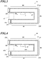
- FIG. 3 is a schematic diagram of an RFID tag of Modification 1.
- FIG. 4 is a schematic diagram of an RFID tag of Modification 2.
- the RFID tags 1A, 1B of Modification 1 and Modification 2 have one spacer 42 or spacers 42a, 42b inside the folded portion of the film wiring board 10.
- the one spacer 42 or the spacers 42a, 42b do not fill the entire inner space G0, which is made by folding. Specifically, the one spacer 42 or the spacers 42a, 42b do not fill a partial range of the space GO in the longitudinal direction (longitudinal direction of the base material 11 on the radiant conductor 21A). They are arranged so as to leave a gap in one part in the longitudinal direction.
- the spacers 42, 42a, 42b may be flexible.
- the spacers 42, 42a, 42b keep the height of the space GO (height in the direction perpendicular to the radiant conductor 21A).
- the RFID tags 1A, 1B are attached to a curved surface having a curvature in the longitudinal direction of the space G0, the RFID tags 1A, 1B can be flexibly deformed along the curved surface.
- the one spacer 42, or one spacer 42a of the two, is constituted by a dielectric (e.g. polyimide).
- the spacers 42, 42a are placed on the opposite side of the short-circuit conductor 21B across the center of the space G0.
- a strong electric field is generated between the radiant conductor 21A and the ground conductor 21C on the opposite side (open end side) of the short-circuit conductor 21B. Since the spacer 42, which is a dielectric, is present in this range, the electric field is intensified and antenna gain is improved.
- the increase in the dielectric constant at the open end side achieves advantageous effect of shortening the wavelength of radio waves.
- the RFID tags 1A, 1B are made smaller.
- Both the top and the bottom of each of the spacers 42, 42a, 42b in FIGS. 3 and 4 may be bonded to the back side of the film wiring board 10.
- the bonding of the spacers 42, 42a, 42b keeps the folding of the film wiring board 10. In that case, as in the examples shown in FIGS. 3 and 4 , one folding region R5 and the third region R3 in Embodiment 1 may be omitted.
- FIG. 5 is a schematic diagram of an RFID tag of Embodiment 2 of the present disclosure.
- FIG. 6 shows a circuit configuration of the RFID tag of Embodiment 2.
- FIG. 7 is an illustration in which a film wiring board of the RFID tag of FIG. 5 is unfolded.
- the same signs are given to the same elements as those in Embodiment 1. Detailed description is omitted.
- the capacitive conductor 27, the wiring conductor 25a, and connection pads 26a, 26b are added on the back side of the first region R1.
- the capacitive conductor 27 is disposed opposite the ground conductor 21C across the base material 11.
- the capacitive conductor 27 is wider than the wiring conductor 25 in the width direction of the base material 11, and has a larger area than the short-circuit conductor 21B.
- the connection pad 26a is located at one end of the wiring conductor 25a.
- the connection pad 26b is placed behind the ground conductor 21C.
- the connection pad 26b is connected to the ground conductor 21C via the via conductor 32C.
- one end of the wiring conductor 25 is connected to the connection pad 22b on the front side via the via conductor 32d.
- the other end of the wiring conductor 25 is connected to the capacitive conductor 27 in the first region R1.
- a wiring conductor 21D and the connection pads 22a, 22b are added on the front side of the film wiring board 10C.
- the wiring conductor 21D extends from the radiant conductor 21A to the third region R3 on the opposite side of the short-circuit conductor 21B.
- the connection pad 22a is located at one end of the wiring conductor 21D.
- the connection pad 22b is connected to the connection pad 26b on the back side via the via conductor 32d.
- connection pads 22a, 22b on the front side and the connection pads 26a, 26b on the back side are arranged such that the connection pads 22a, 22b overlap the connection pads 26a, 26b respectively when the first region R1 and the third region R3 of the film wiring board 10C are stacked.
- the radiant conductor 21A on the front side is an example of the first conductor portion according to the present disclosure.
- the ground conductor 21C on the front side is an example of the "second conductor portion included in the conductor on the first side” according to the present disclosure.
- the wiring conductors 25, 25a, the connection pads 26a, 26b, and the capacitive conductor 27 on the back side are an example of the "conductors on the second side other than the second conductor portion" according to the present disclosure.
- the folding region R4 and the folding region R5 are folded.
- the first region where the ground conductor 21C is disposed and the third region where the connection pads 22a, 22b are disposed are in close proximity and are opposite to each other.
- the short-circuit conductor 21B is placed in the folding region R4.
- the wiring conductor 21D is placed in the folding region R5.
- the connection pad 22a on the front side is bonded to the connection pad 26a on the back side via a conductive bonding material 45a.
- the connection pad 22b on the front side is bonded to the connection pad 26b on the back side via a conductive bonding material 45b.
- the space GO higher than the RFID IC 2 may be provided inside the folded portion of the film wiring board 10C.
- a spacer 42x may be disposed in the space G0.
- the spacer 42x may be flexible.
- capacitance C1 is configured between the capacitive conductor 27 and the ground conductor 21C.
- the signal terminal of the RFID IC 2 is connected to the capacitive conductor 27 and the radiant conductor 21A via the wiring conductor 25.
- a capacitively loaded plate-shaped inverse F antenna is configured.
- a small RFID tag 1C having good antenna characteristics is realized.
- the Flexibility of the RFID tag 1C is improved by making the film wiring board 10C thinner. If the film wiring board 10C is thin, the distance between the radiant conductor 21A and the ground conductor 21C is not secured. It decreases the impedance of antenna and makes it difficult to match the output impedance of the RFID IC 2.
- the wiring conductor 25 which is connected to the RFID IC 2 is connected to the ground conductor 21C and the capacitance C1 with a high voltage. It increases the impedance of antenna. The output impedance of the RFID IC 2 and the impedance of antenna can be easily matched.
- the wiring conductor 25 may be connected to the capacitive conductor 27 at a position on the capacitive conductor 27 which is near the short-circuit conductor 21B and be connected to the ground conductor 21C at a position on the ground conductor 21C which is far from the short-circuit conductor 21B. It increases the impedance of antenna.
- FIG. 8 is a schematic diagram of an RFID tag of Modification 3.
- FIG. 9 shows a circuit configuration of the RFID tag of Modification 3.
- FIG. 10 is a schematic diagram of an RFID tag of Modification 4.
- FIG. 11 is a schematic diagram of an RFID tag of Modification 5.
- the RFID tags 1D, 1E, 1F of Modifications 3, 4, and 5 are the same as the RFID tag 1C of Embodiment 2 except for configurations of spacers 42, 42a-42f.
- the spacers 42, 42a-42f of Modifications 3, 4, and 5 do not fill the entire inner space GO made by folding the film wiring board 10C. They are arranged to leave a gap in a partial range of the space GO in the longitudinal direction.
- the spacers 42a-42d may be flexible.
- the RFID tags 1D-1F are attached to a curved surface having a curvature in the longitudinal direction of the space G0, the RFID tags 1D, 1E, 1F can be flexibly deformed along the curved surface.
- the spacers 42, 42a-42f the spacers 42, 42a, 42c disposed farthest away from the short-circuit conductor 21B may be constituted by dielectrics (e.g., polyimide).
- Other spacers 42b, 42d-42f may also be dielectrics.
- FIG. 9 also in a circuit configuration with the capacitance C1, a strong electric field is generated on the opposite side (open end side) of the short-circuit conductor 21B when radio waves are transmitted. Since the spacers 42, 42a, 42c, which are dielectrics, are present in this range, antenna gain is improved. Further, effect of shortening the wireless wavelength makes the antenna smaller.
- Both the top and the bottom of each of the spacers 42, 42a-42f in FIGS. 7 and 10-11 may be bonded to the back side of the film wiring board 10C.
- the bonding of the spacers 42, 42a-42f keeps the folding of the film wiring boards 10D-10F.
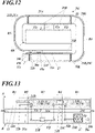
- FIG. 12 is a schematic diagram of the RFID tag of Modification 6.
- FIG. 13 is an illustration in which a film wiring board of the RFID tag of Modification 6 is unfolded.
- the main difference of the RFID tag 1G of Modification 6 is that the wiring conductor 25 of Embodiment 2 is replaced by wiring conductors 25A-25D of different patterns.
- Other elements are the same as those of the RFID tag 1C of Embodiment 2. Differences are explained in detail below.
- conductors connecting the RFID IC 2 to the capacitive conductor 27 and the ground conductor 21C include the wiring conductors 25A, 25C on the front side, the wiring conductors 25B, 25D on the back side, and via conductors 32c, 32e-32g.
- the wiring conductor 25A, the via conductor 32e, the wiring conductor 25B, the via conductor 32f, the wiring conductor 25C, the via conductor 32g, and the wiring conductor 25D line up in this order.
- the wiring conductors 25A, 25C on the front side are placed in the folding regions R4, R5.
- the radiant conductor 21A on the front side is an example of the first conductor portion according to the present disclosure.
- the ground conductor 21C on the front side is an example of the "second conductor portion included in the conductor on the first side” according to the present disclosure.
- the wiring conductors 25B, 25D, the connection pads 26a, 26b, and the capacitive conductor 27 on the back side are an example of the "conductors on the second side other than the second conductor portion" according to the present disclosure.
- This configuration realizes a configuration without conductors on the backside in the folding regions R4, R5.
- the configuration having conductors only on one side achieves flexibility of the film wiring board 10G in folding, suppresses deterioration of conductors due to folding, and improves durability of the RFID tag 1G.
- the longer connection path between the RFID IC 2 and the capacitive conductor 27 increases the impedance of antenna.
- FIG. 14 is a schematic diagram of an RFID tag of Embodiment 3 of the present disclosure.
- FIG. 15 is an illustration in which a film wiring board of the RFID tag of FIG. 14 is unfolded.
- FIG. 16 is a schematic diagram of an RFID tag of Embodiment 4 of the present disclosure.
- FIG. 17 is an illustration in which film wiring of the RFID tag of FIG. 16 is unfolded.
- the capacitive conductor 27H of Embodiment 3 is provided on the front side of the third region R3 of the film wiring board 10H.
- the capacitive conductor 27H is connected to the radiant conductor 21A via the wiring conductor 21D.
- the connection pad 22b is provided on the front side of the third region R3 of the film wiring board 10H.
- One end of the wiring conductor 25 on the back side is connected to the connection pad 22b via the via conductor 32d.
- a connection pad 26h and the connection pad 26b are provided on the back side of the first region R1 of the film wiring board 10H.
- the connection pad 26h is connected to one end of the wiring conductor 25.
- the connection pad 26b is connected to the ground conductor 21C via the via conductor 32c.
- connection pad 22b and the capacitive conductor 27H on the front side are arranged such that they overlap the connection pads 26b, 26h on the back side respectively when the film wiring board 10H is folded to stack the first region R1 and the third region R3.
- the capacitive conductor 27H and the ground conductor 21C are arranged to face each other.
- the radiant conductor 21A on the front side is an example of the first conductor portion according to the present disclosure.
- the ground conductor 21C on the front side is an example of the "second conductor portion included in the conductor on the first side” according to the present disclosure.
- the wiring conductor 25 on the back side is an example of the "conductor on the second side other than the second conductor portion" according to the present disclosure.
- connection pad 26h on the back side is bonded to a part of the capacitive conductor 27H via a conductive bonding material 45h in a state where the film wiring board 10H is folded.
- the connection pad 26b on the back side is bonded to the connection pad 22b on the front side via the conductive bonding material 45b.
- One end of a wiring conductor extending from the capacitive conductor 27H may be bonded to the connection pad 26h on the backside.
- capacitance is configured between the capacitive conductor 27H and the ground conductor 21C.
- a part of the capacitive conductor 27H is connected to the radiant conductor 21A via the wiring conductor 21D.
- Another part of the capacitive conductor 27H is connected to the signal terminal of the RFID IC 2 via the wiring conductor 25.
- the capacitive conductor 271 of Embodiment 4 is provided on the back side of the third region R3 of the film wiring board 10I.
- a connection pad 22j is provided on the front side of the third region R3 of the film wiring board 10I.
- the connection pad 22j is connected to the capacitive conductor 271 via a via conductor 32h.
- a part of the capacitive conductor 271 is connected to one end of the wiring conductor 21D on the front side via the via conductor 32i.
- connection pads 22b, 22j on the front side are connected to the connection pads 26b, 26h on the back side via the conductive bonding materials 45b, 45h in a state where the film wiring board 101 is folded.
- the capacitive conductor 271 and the ground conductor 21C are opposite each other.
- the radiant conductor 21A on the front side is an example of a first conductor portion according to the present disclosure.
- the ground conductor 21C on the front side is an example of the "second conductor portion included in the conductor on the first side” according to the present disclosure.
- the wiring conductor 25 and the capacitive conductor 271 on the back side are an example of the "conductors on the second side other than the second conductor portion" according to the present disclosure.
- capacitance is configured between the capacitive conductor 271 and the ground conductor 21C.
- a part of the capacitive conductor 271 is connected to the radiant conductor 21A via the via conductor 32i and the wiring conductor 21D.
- Another part of the capacitive conductor 271 is connected to the wiring conductor 25 via the via conductor 32h.
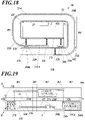
- FIG. 18 is a schematic diagram of an RFID tag of Modification 7.
- FIG. 19 is an illustration in which a film wiring board of the RFID tag of FIG. 18 is unfolded.
- the RFID tag 1K of Modification 7 differs from Embodiment 4 mainly in that a ground conductor 21Ck is provided on the back side of the first region R1. Other elements are the same as those in Embodiment 4. Differences are explained in detail below.
- the ground conductor 21Ck of Modification 7 is connected to the short-circuit conductor 21B via a via conductor 32k.
- the radiant conductor 21A on the front side is an example of the first conductor portion according to the present disclosure.
- the ground conductor 21Ck on the back side is an example of the "second conductor portion included in the conductor on the second side” according to the present disclosure.
- the wiring conductor 25, the connection pad 26h, and the capacitive conductor 271 on the back side are an example the "conductors on the second side other than the second conductor portion" according to the present disclosure.
- Such a configuration also configures a plate-shaped inverted F antenna in which the ground conductor 21Ck and the radiant conductor 21A are arranged opposite to each other and are short-circuited by the short-circuit conductor 21B.
- the capacitive conductor 271 is disposed opposite to the ground conductor 21Ck to form capacitance. It realizes a capacitively loaded plate-shaped inverse F antenna.
- FIG. 20 is an illustration in which a film wiring board of an RFID tag of Embodiment 5 of the present disclosure is unfolded.
- the wiring conductor 25 in Embodiment 2 is replaced by a wiring conductor 25J provided on the front side of the film wiring board 10J.
- the wiring conductor 25J is provided at a position away from the radiant conductor 21A, the short-circuit conductor 21B, the ground conductor 21C, and the wiring conductor 21D in the width direction of the base material 11.
- One end of the wiring conductor 25J is connected to the connection pad 22j.
- the other end of the wiring conductor 25J is connected to the capacitive conductor 27 via the via conductor 32j.
- the capacitive conductor 27, the connection pads 26a, 26b, and the wiring conductor 25a connecting the capacitive conductor 27 and the connection pad 26a are provided at positions which are on the back side of the film wiring board 10J and which are behind the ground conductor 21C.
- the RFID IC 2 in the wiring conductor 25J is provided on the front side of the film wiring board 10J.
- the RFID IC 2 is mounted on the front side of the film wiring board 10J.
- the radiant conductor 21A on the front side is an example of the first conductor portion according to the present disclosure.
- the ground conductor 21C on the front side is an example of the "second conductor portion included in the conductor on the first side” according to the present disclosure.
- the wiring conductor 25a, the connection pads 26a, 26b, and the capacitive conductor 27 on the back side are an example of the "conductors of the second side other than the second conductor portion" according to the present disclosure.
- the RFID IC 2 faces outward and is located on the outer side in a state where the film wiring board 10J is folded. Therefore, the RFID IC 2 can be easily replaced.
- the wiring conductor 25J and the RFID IC 2 are provided on the front side of the film wiring board 10J and are aligned with the radiant conductor 21A in the width direction of the base material 11.
- the wiring conductor 25J and the RFID IC 2 are provided on the back side of the film wiring board 10J and overlap with the radiant conductor 21A and the ground conductor 21C.
- the RFID IC 2 is placed at a position where it overlaps with the radiating conductor 21A and the ground conductor 21C. It makes the base material 11 shorter in the width direction. It is advantageous in terms of miniaturization.
- the RFID IC 2 is placed at the center of the base material 11 in the width direction. It improves protection of the RFID IC 2 and durability of the RFID tag 1.
- FIG. 21 is a perspective view of the RFID tag of Embodiment 2 used in simulation.
- FIG. 22 is a side view of the RFID tag of FIG. 21 .
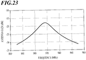
- FIG. 23 is a graph showing frequency characteristics of antenna gain of the RFID tag of FIG. 21 and FIG. 22 .
- the size of the RFID tag was 5 mm in the X direction, 10 mm in the Y direction, and 1 mm in the Z direction.
- Polyimide was used as the spacer 42x.
- the X direction is the width direction of the base material 11.
- the Y direction is the longitudinal direction of the base material 11.
- the Z direction is the direction in which the radiant conductor 21A and the ground conductor 21C overlap, and is the vertical direction of the radiant conductor 21A.
- frequency characteristics of antenna are easily matched to the transmission frequency band (920 MHz band) of the RFID IC 2.
- antenna gain of more than -20 dBi was obtained.
- the RFID tags 1, 1A-1J of the embodiment include the flexible film wiring boards 10, 10C, 10H-10J.
- the RFID IC 2 is mounted on the film wiring boards 10, 10C, 10H-10J.
- the film wiring boards 10, 10C, 10H-10J are folded so that the radiant conductor 21A and the ground conductor 21C on the front side and conductors on the back side (such as the wiring conductor 25 and the capacitive conductor 27) overlap in the direction perpendicular to the plane of the radiant conductor 21A. They constitute an antenna in which three or more layers of conductors are layered. Small RFID tags 1, 1A-1J with improved antenna characteristics are realized.
- Embodiments of the present invention are described above.
- the RFID tags of the present disclosure are not limited to the above embodiments.
- the above embodiments show configurations in which the film wiring board is folded so that the first region and the second region overlap or the first region to the third region overlap.
- a configuration in which the film wiring board is folded so that more regions overlap may be employed.
- the details specifically indicated in the embodiments, such as the material of the base material of the film wiring board and the material of the spacer, may be changed as appropriate within the scope of the claims of the invention.
- the present disclosure can be utilized in RFID tags.
Landscapes
- Engineering & Computer Science (AREA)
- Microelectronics & Electronic Packaging (AREA)
- Computer Hardware Design (AREA)
- Physics & Mathematics (AREA)
- General Physics & Mathematics (AREA)
- Theoretical Computer Science (AREA)
- Computer Networks & Wireless Communication (AREA)
- Details Of Aerials (AREA)
Abstract
Description
- The present disclosure relates to an RFID (radio frequency identifier) tag.
- In a conventional RFID tag, an antenna conductor is formed on an insulating board of sintered ceramic, and an IC (integrated circuit) for RFID is mounted on the insulating board. According to an RFID tag described in
WO 2018/016624A , an antenna conductor laminated on an insulating board realizes a compact tag with excellent wireless communication characteristics. - An RFID tag according to the present disclosure includes:
- a film wiring board that comprises:
- a base material which is flexible and which includes a first side and a second side opposite the first side; and
- conductors located on the first side and the second side; and
- an RFID IC connected to the conductors,
- wherein the film wiring board is folded so that at least a first conductor portion included in a conductor on the first side, a second conductor portion included in a conductor on the first side or the second side, and a conductor on the second side other than the second conductor portion overlap.
-
-
FIG. 1 is a schematic diagram of an RFID tag ofEmbodiment 1 of the present disclosure. -
FIG. 2 is an illustration in which a film wiring board of the RFID tag inFIG. 1 is unfolded. -
FIG. 3 is a schematic diagram of an RFID tag ofModification 1. -
FIG. 4 is a schematic diagram of an RFID tag ofModification 2. -
FIG. 5 is a schematic diagram of an RFID tag ofEmbodiment 2 of the present disclosure. -
FIG. 6 shows a circuit configuration of the RFID tag ofEmbodiment 2. -
FIG. 7 is an illustration in which a film wiring board of the RFID tag ofFIG. 5 is unfolded. -
FIG. 8 is a schematic diagram of an RFID tag of Modification 3. -
FIG. 9 shows a circuit configuration of the RFID tag of Modification 3. -
FIG. 10 is a schematic diagram of an RFID tag of Modification 4. -
FIG. 11 is a schematic diagram of an RFID tag of Modification 5. -
FIG. 12 is a schematic diagram of the RFID tag of Modification 6. -
FIG. 13 is an illustration in which a film wiring board of the RFID tag ofFIG. 12 is unfolded. -
FIG. 14 is a schematic diagram of an RFID tag of Embodiment 3 of the present disclosure. -
FIG. 15 is an illustration in which a film wiring board of the RFID tag ofFIG. 14 is unfolded. -
FIG. 16 is a schematic diagram of an RFID tag of Embodiment 4 of the present disclosure. -
FIG. 17 is an illustration in which a film wiring board of the RFID tag ofFIG. 16 is unfolded. -
FIG. 18 is a schematic diagram of an RFID tag of Modification 7. -
FIG. 19 is an illustration in which a film wiring board of the RFID tag ofFIG. 18 is unfolded. -
FIG. 20 is an illustration in which a film wiring board of an RFID tag of Embodiment 5 of the present disclosure is unfolded. -
FIG. 21 is a perspective view of the RFID tag ofEmbodiment 2 used in simulation. -
FIG. 22 is a side view of the RFID tag ofFIG. 21 . -
FIG. 23 is a graph showing frequency characteristics of antenna gain of the RFID tag ofFIG. 21 . - Embodiments of the present disclosure will be described in detail below with reference to the drawings.
-
FIG. 1 is a schematic diagram of an RFID tag ofEmbodiment 1 of the present disclosure.FIG. 2 is an illustration in which a film wiring board of the RFID tag inFIG. 1 is unfolded. - Illustrations of film wiring boards being unfolded, from
FIG. 2 onward, show: - a conductor pattern A on the front side when the film wiring board is viewed from the front side; and
- a conductor pattern B on the back side seen through from the front side.
- The
RFID tag 1 ofEmbodiment 1 includes thefilm wiring board 10 and anRFID IC 2. The RFID IC2 communicates wirelessly with a reader/writer using, for example, UHF (ultra high frequency) band radio waves. Thefilm wiring board 10 may be FPC (flexible printed circuits). - The
film wiring board 10 includes: - a flexible and pliable film-
like base material 11; - conductors (21A-21C, 25) laminated on the front and back sides of the
base material 11; and - via
conductors base material 11. - The conductors (21A-21C, 25) of the
base material 11 are conductor films fixed to thebase material 11. The front side of each conductor may be covered with an insulating film. The material of thebase material 11 is, for example, polyimide. The front and back sides of thebase material 11 are examples of the first and second sides of the present disclosure. - Conductors on the front side include a
radiant conductor 21A, a short-circuit conductor 21B, and aground conductor 21C. Theradiant conductor 21A, the short-circuit conductor 21B, and theground conductor 21 C are lined up in this order in the longitudinal direction of thebase material 11. Each of theradiant conductor 21A and theground conductor 21C is wider than the short-circuit conductor 21B in the width direction of thebase material 11 and has a larger area than the short-circuit conductor 21B. Theradiant conductor 21A and theground conductor 21C are advantageous in terms of miniaturization if they extend to the end of thebase material 11 in the width direction. In that case, to prevent short circuit due to contact with an external conductive object, as in the example shown inFIG. 2 , theradiant conductor 21A and theground conductor 21C may extend to a position slightly inner than the end of thebase material 11 in the width direction. - The conductor on the back side includes a
wiring conductor 25 to which a signal terminal and a ground terminal of theRFID IC 2 are connected. The width of thewiring conductor 25 in the width direction of thebase material 11 is narrower than theradiant conductor 21A and theground conductor 21C. A part of thewiring conductor 25 is located behind theradiant conductor 21A and theground conductor 21C. The RFID IC 2 is connected to thewiring conductor 25 via, for example, a conductive bonding material. A connection part of the RFID IC2 in thewiring conductor 25 is placed behind theradiant conductor 21A. Alternatively, it may be placed behind theground conductor 21C. - The via
conductor 32b connects thewiring conductor 25 with theground conductor 21C. Thewiring conductor 25 may be connected with theground conductor 21C at a position farther from theRFID IC 2. The impedance of antenna can be increased by increasing the connection distance between theRFID IC 2 and theground conductor 21C. It easily matches the output impedance of the RFID IC2 with the impedance of antenna. TheRFID IC 2 may be placed in the center of the second region R2 in the longitudinal direction. The impedance can be further increased by positioning theRFID IC 2 away from theground conductor 21C. If thewiring conductor 25 is made longer and theRFID IC 2 is mounted in a folding region R5 or the third region R3, the distance between theRFID IC 2 and theground conductor 21 C (distance in the thickness direction of the RFID tag 1) becomes shorter. It decreases the impedance. Accordingly, theRFID IC 2 may be mounted at a position in the second region R2, the position being farthest from the first region R1 where theground conductor 21C is located and being close to the folding region R5. - A
wiring conductor 25 extending to the first region R1 from the connection portion of theRFID IC 2 may be extended to the third region R3. In that case, a via conductor and a connection pad connected to the via conductor may be provided on the front side of the third region R3. The via conductor is connected to thewiring conductor 25 on the back side of the third region R3 and penetrates to the front side. A connection pad may be provided on the back side of the first region R1, and a via conductor and a connection pad connected to the via conductor may be provided on the front side of the first region R1. The via conductor is connected to the connection pad provided on the back side of the first region R1 and penetrates to the front side. A conductive bonding material may connect the connection pad on the front side of the third region R3 with the connection pad in the first region R1. In the arrangement of thewiring conductor 25 according toEmbodiment 1, there are few electrical connection points by the conductive bonding material. It improves reliability. - In
Embodiment 1, theradiant conductor 21A on the front side is an example of the first conductor portion according to the present disclosure. Theground conductor 21C on the front side is an example of the "second conductor portion included in the conductor on the first side" according to the present disclosure. Thewiring conductor 25 on the back side is an example of the "conductor on the second side other than the second conductor portion" according to the present disclosure. - The via
conductor 32a connects one end of thewiring conductor 25 to theradiant conductor 21A. The viaconductor 32b connects the other end of thewiring conductor 25 to theground conductor 21C. The viaconductor 32a may be disposed on the side of theradiant conductor 21A which is farther from the short-circuit conductor 21B than the center. The viaconductor 32b may be disposed on the side of theground conductor 21C which is farther from the short-circuit conductor 21B than the center. - As shown in
FIGS. 1 and 2 , folding regions R4, R 5 of thefilm wiring board 10 are folded. The first region R1 having theground conductor 21C, the second region R2 having the radiatingconductor 21 A, and the third region R3 overlap. Portions of the first region R1 and the third region R3 are joined together with abonding material 41 to keep the fold. As the folding regions R4 and R5, a region where the short-circuit conductor 21B and thewiring conductor 25 are disposed and a region where no conductor is disposed are employed. - In a state where the
film wiring board 10 is folded, theradiant conductor 21A and theground conductor 21 C face outward and are located on the outside of theRFID tag 1. Thewiring conductor 25 and theRFID IC 2 face inward and are located inside theRFID tag 1. A space GO which is higher than theRFID IC 2 may be provided inside thefilm wiring board 10 which is folded and wound. - In the
RFID tag 1 configured as described above, theradiant conductor 21A, which is the first conductor portion, and theground conductor 21C, which is the second conductor portion, overlap facing opposite sides. Edges of theradiant conductor 21A and theground conductor 21C are connected to each other via the short-circuit conductor 21B. The signal terminal of theRFID IC 2 is connected to a portion of theradiant conductor 21A via thewiring conductor 25 and the viaconductor 32b, the portion being far from the short-circuit conductor 21B. The contact point between theradiant conductor 21A and the viaconductor 32b is a power feed point. Theradiant conductor 21A, the short-circuit conductor 21B, and theground conductor 21C constitute a plate-shaped inverted F antenna. Such a configuration achieves miniaturization of theRFID tag 1 and good antenna characteristics of theRFID tag 1. - According to the above configuration, the
RFID IC 2 is placed inside the foldedfilm wiring board 10. Therefore, theRFID IC 2 is protected by the flexiblefilm wiring board 10. It improves durability of theRFID tag 1. TheRFID IC 2 does not protrude outward from thefilm wiring board 10. It achieves miniaturization. - In the examples shown in
FIGS. 1 and 2 , the third region R3 extends to a position where it overlaps theradiant conductor 21A and theground conductor 21C and is bonded to the first region R1. The third region R3 extends further from the bonded position toward the short-circuit conductor 21B. The fold can be kept without connection of the third region R3 between theradiant conductor 21A and theground conductor 21C, i.e., without the portion of the third region R3 beyond the bonded portion (where thebonding material 41 is located). On the other hand, in a case where the third region R3 is arranged to extend to the space between theradiant conductor 21A and theground conductor 21C, the same effect is achieved as in a case wherespacers Modifications base material 11 which is a dielectric is located between theradiant conductor 21A and theground conductor 21C, antenna gain is improved and miniaturization is achieved. -
FIG. 3 is a schematic diagram of an RFID tag ofModification 1.FIG. 4 is a schematic diagram of an RFID tag ofModification 2. The RFID tags 1A, 1B ofModification 1 andModification 2 have onespacer 42 orspacers film wiring board 10. - The one
spacer 42 or thespacers spacer 42 or thespacers base material 11 on theradiant conductor 21A). They are arranged so as to leave a gap in one part in the longitudinal direction. Thespacers - According to such a configuration, the
spacers radiant conductor 21A). In a case where the RFID tags 1A, 1B are attached to a curved surface having a curvature in the longitudinal direction of the space G0, the RFID tags 1A, 1B can be flexibly deformed along the curved surface. - The one
spacer 42, or onespacer 42a of the two, is constituted by a dielectric (e.g. polyimide). Thespacers circuit conductor 21B across the center of the space G0. When RFID tags 1A, 1B transmit radio waves, a strong electric field is generated between theradiant conductor 21A and theground conductor 21C on the opposite side (open end side) of the short-circuit conductor 21B. Since thespacer 42, which is a dielectric, is present in this range, the electric field is intensified and antenna gain is improved. The increase in the dielectric constant at the open end side achieves advantageous effect of shortening the wavelength of radio waves. The RFID tags 1A, 1B are made smaller. - Both the top and the bottom of each of the
spacers FIGS. 3 and 4 may be bonded to the back side of thefilm wiring board 10. The bonding of thespacers film wiring board 10. In that case, as in the examples shown inFIGS. 3 and 4 , one folding region R5 and the third region R3 inEmbodiment 1 may be omitted. -
FIG. 5 is a schematic diagram of an RFID tag ofEmbodiment 2 of the present disclosure.FIG. 6 shows a circuit configuration of the RFID tag ofEmbodiment 2.FIG. 7 is an illustration in which a film wiring board of the RFID tag ofFIG. 5 is unfolded. In theRFID tag 1C ofEmbodiment 2, the same signs are given to the same elements as those inEmbodiment 1. Detailed description is omitted. - As shown in
FIG. 7 , in thefilm wiring board 10C ofEmbodiment 2, thecapacitive conductor 27, thewiring conductor 25a, andconnection pads capacitive conductor 27 is disposed opposite theground conductor 21C across thebase material 11. Thecapacitive conductor 27 is wider than thewiring conductor 25 in the width direction of thebase material 11, and has a larger area than the short-circuit conductor 21B. Theconnection pad 26a is located at one end of thewiring conductor 25a. Theconnection pad 26b is placed behind theground conductor 21C. Theconnection pad 26b is connected to theground conductor 21C via the via conductor 32C. In the third region R3, one end of thewiring conductor 25 is connected to theconnection pad 22b on the front side via the viaconductor 32d. The other end of thewiring conductor 25 is connected to thecapacitive conductor 27 in the first region R1. - A
wiring conductor 21D and theconnection pads film wiring board 10C. Thewiring conductor 21D extends from theradiant conductor 21A to the third region R3 on the opposite side of the short-circuit conductor 21B. Theconnection pad 22a is located at one end of thewiring conductor 21D. Theconnection pad 22b is connected to theconnection pad 26b on the back side via the viaconductor 32d. - The
connection pads connection pads connection pads connection pads film wiring board 10C are stacked. - In
Embodiment 2, theradiant conductor 21A on the front side is an example of the first conductor portion according to the present disclosure. Theground conductor 21C on the front side is an example of the "second conductor portion included in the conductor on the first side" according to the present disclosure. Thewiring conductors connection pads capacitive conductor 27 on the back side are an example of the "conductors on the second side other than the second conductor portion" according to the present disclosure. - In the
RFID tag 1C ofEmbodiment 2, the folding region R4 and the folding region R5 are folded. The first region where theground conductor 21C is disposed and the third region where theconnection pads circuit conductor 21B is placed in the folding region R4. Thewiring conductor 21D is placed in the folding region R5. In a state where thefilm wiring board 10C is folded, theconnection pad 22a on the front side is bonded to theconnection pad 26a on the back side via aconductive bonding material 45a. Theconnection pad 22b on the front side is bonded to theconnection pad 26b on the back side via aconductive bonding material 45b. The space GO higher than theRFID IC 2 may be provided inside the folded portion of thefilm wiring board 10C. Aspacer 42x may be disposed in the space G0. Thespacer 42x may be flexible. - According to such a conductor pattern, as shown in
FIG. 6 , capacitance C1 is configured between thecapacitive conductor 27 and theground conductor 21C. The signal terminal of theRFID IC 2 is connected to thecapacitive conductor 27 and theradiant conductor 21A via thewiring conductor 25. Thus, a capacitively loaded plate-shaped inverse F antenna is configured. Asmall RFID tag 1C having good antenna characteristics is realized. - Flexibility of the
RFID tag 1C, which is made by folding thefilm wiring board 10C, is improved by making thefilm wiring board 10C thinner. If thefilm wiring board 10C is thin, the distance between theradiant conductor 21A and theground conductor 21C is not secured. It decreases the impedance of antenna and makes it difficult to match the output impedance of theRFID IC 2. However, according to theRFID tag 1C ofEmbodiment 2, thewiring conductor 25 which is connected to theRFID IC 2 is connected to theground conductor 21C and the capacitance C1 with a high voltage. It increases the impedance of antenna. The output impedance of theRFID IC 2 and the impedance of antenna can be easily matched. - As in the embodiment, the
wiring conductor 25 may be connected to thecapacitive conductor 27 at a position on thecapacitive conductor 27 which is near the short-circuit conductor 21B and be connected to theground conductor 21C at a position on theground conductor 21C which is far from the short-circuit conductor 21B. It increases the impedance of antenna. -
FIG. 8 is a schematic diagram of an RFID tag of Modification 3.FIG. 9 shows a circuit configuration of the RFID tag of Modification 3.FIG. 10 is a schematic diagram of an RFID tag of Modification 4.FIG. 11 is a schematic diagram of an RFID tag of Modification 5. - The RFID tags 1D, 1E, 1F of Modifications 3, 4, and 5 are the same as the
RFID tag 1C ofEmbodiment 2 except for configurations ofspacers spacers film wiring board 10C. They are arranged to leave a gap in a partial range of the space GO in the longitudinal direction. Thespacers 42a-42d may be flexible. - According to this configuration, in a case where RFID tags 1D-1F are attached to a curved surface having a curvature in the longitudinal direction of the space G0, the
RFID tags 1D, 1E, 1F can be flexibly deformed along the curved surface. - Of the
spacers spacers circuit conductor 21B may be constituted by dielectrics (e.g., polyimide).Other spacers FIG. 9 , also in a circuit configuration with the capacitance C1, a strong electric field is generated on the opposite side (open end side) of the short-circuit conductor 21B when radio waves are transmitted. Since thespacers - Both the top and the bottom of each of the
spacers FIGS. 7 and10-11 may be bonded to the back side of thefilm wiring board 10C. The bonding of thespacers film wiring boards 10D-10F. -
FIG. 12 is a schematic diagram of the RFID tag of Modification 6.FIG. 13 is an illustration in which a film wiring board of the RFID tag of Modification 6 is unfolded. The main difference of theRFID tag 1G of Modification 6 is that thewiring conductor 25 ofEmbodiment 2 is replaced by wiringconductors 25A-25D of different patterns. Other elements are the same as those of theRFID tag 1C ofEmbodiment 2. Differences are explained in detail below. - In the
film wiring board 10G of theRFID tag 1G of Modification 6, conductors connecting theRFID IC 2 to thecapacitive conductor 27 and theground conductor 21C include thewiring conductors conductors conductors wiring conductor 25A, the viaconductor 32e, thewiring conductor 25B, the viaconductor 32f, thewiring conductor 25C, the viaconductor 32g, and thewiring conductor 25D line up in this order. Thewiring conductors - In Modification 6, the
radiant conductor 21A on the front side is an example of the first conductor portion according to the present disclosure. Theground conductor 21C on the front side is an example of the "second conductor portion included in the conductor on the first side" according to the present disclosure. The wiringconductors connection pads capacitive conductor 27 on the back side are an example of the "conductors on the second side other than the second conductor portion" according to the present disclosure. - This configuration realizes a configuration without conductors on the backside in the folding regions R4, R5. In the folding regions R4, R5, the configuration having conductors only on one side achieves flexibility of the
film wiring board 10G in folding, suppresses deterioration of conductors due to folding, and improves durability of theRFID tag 1G. The longer connection path between theRFID IC 2 and thecapacitive conductor 27 increases the impedance of antenna. -
FIG. 14 is a schematic diagram of an RFID tag of Embodiment 3 of the present disclosure.FIG. 15 is an illustration in which a film wiring board of the RFID tag ofFIG. 14 is unfolded.FIG. 16 is a schematic diagram of an RFID tag of Embodiment 4 of the present disclosure.FIG. 17 is an illustration in which film wiring of the RFID tag ofFIG. 16 is unfolded. - In the
RFID tag 1H of Embodiment 3, arrangement and a connection position of acapacitive conductor 27H on the circuit are different from those of thecapacitive conductor 27 ofEmbodiment 2. Other elements are the same as those inEmbodiment 2. In the RFID tag 1I of Embodiment 4, arrangement and a connection position of acapacitive conductor 271 in the circuit are different from those of thecapacitive conductor 27H of Embodiment 3. Other elements are the same as those in Embodiment 3. Differences are explained in detail below. - As shown in
FIG. 15 , thecapacitive conductor 27H of Embodiment 3 is provided on the front side of the third region R3 of thefilm wiring board 10H. Thecapacitive conductor 27H is connected to theradiant conductor 21A via thewiring conductor 21D. Theconnection pad 22b is provided on the front side of the third region R3 of thefilm wiring board 10H. One end of thewiring conductor 25 on the back side is connected to theconnection pad 22b via the viaconductor 32d. Aconnection pad 26h and theconnection pad 26b are provided on the back side of the first region R1 of thefilm wiring board 10H. Theconnection pad 26h is connected to one end of thewiring conductor 25. Theconnection pad 26b is connected to theground conductor 21C via the viaconductor 32c. Theconnection pad 22b and thecapacitive conductor 27H on the front side are arranged such that they overlap theconnection pads film wiring board 10H is folded to stack the first region R1 and the third region R3. Thecapacitive conductor 27H and theground conductor 21C are arranged to face each other. - In Embodiment 3, the
radiant conductor 21A on the front side is an example of the first conductor portion according to the present disclosure. Theground conductor 21C on the front side is an example of the "second conductor portion included in the conductor on the first side" according to the present disclosure. Thewiring conductor 25 on the back side is an example of the "conductor on the second side other than the second conductor portion" according to the present disclosure. - As shown in
FIG. 14 , in theRFID tag 1H of Embodiment 3, theconnection pad 26h on the back side is bonded to a part of thecapacitive conductor 27H via aconductive bonding material 45h in a state where thefilm wiring board 10H is folded. Theconnection pad 26b on the back side is bonded to theconnection pad 22b on the front side via theconductive bonding material 45b. One end of a wiring conductor extending from thecapacitive conductor 27H may be bonded to theconnection pad 26h on the backside. - In such a configuration, capacitance is configured between the
capacitive conductor 27H and theground conductor 21C. A part of thecapacitive conductor 27H is connected to theradiant conductor 21A via thewiring conductor 21D.
Another part of thecapacitive conductor 27H is connected to the signal terminal of theRFID IC 2 via thewiring conductor 25. Such a configuration realizes a capacitively loaded plate-shaped inverse F antenna as inEmbodiment 2. - As shown in
FIG. 17 , thecapacitive conductor 271 of Embodiment 4 is provided on the back side of the third region R3 of the film wiring board 10I. Aconnection pad 22j is provided on the front side of the third region R3 of the film wiring board 10I. Theconnection pad 22j is connected to thecapacitive conductor 271 via a viaconductor 32h. A part of thecapacitive conductor 271 is connected to one end of thewiring conductor 21D on the front side via the viaconductor 32i. - As shown in
FIG. 16 , in the RFID tag 1I of Embodiment 4, theconnection pads connection pads conductive bonding materials film wiring board 101 is folded. Thecapacitive conductor 271 and theground conductor 21C are opposite each other. - In Embodiment 4, the
radiant conductor 21A on the front side is an example of a first conductor portion according to the present disclosure. Theground conductor 21C on the front side is an example of the "second conductor portion included in the conductor on the first side" according to the present disclosure. Thewiring conductor 25 and thecapacitive conductor 271 on the back side are an example of the "conductors on the second side other than the second conductor portion" according to the present disclosure. - In such a configuration, capacitance is configured between the
capacitive conductor 271 and theground conductor 21C. A part of thecapacitive conductor 271 is connected to theradiant conductor 21A via the viaconductor 32i and thewiring conductor 21D. Another part of thecapacitive conductor 271 is connected to thewiring conductor 25 via the viaconductor 32h. Such a configuration realizes a capacitively loaded plate-shaped inverse F antenna as inEmbodiment 2. -
FIG. 18 is a schematic diagram of an RFID tag of Modification 7.FIG. 19 is an illustration in which a film wiring board of the RFID tag ofFIG. 18 is unfolded. The RFID tag 1K of Modification 7 differs from Embodiment 4 mainly in that a ground conductor 21Ck is provided on the back side of the first region R1. Other elements are the same as those in Embodiment 4. Differences are explained in detail below. - The ground conductor 21Ck of Modification 7 is connected to the short-
circuit conductor 21B via a viaconductor 32k. - Connection between the ground conductor 21Ck and the
wiring conductor 25 on the front side is achieved by: - joint between a part 26bk of the ground conductor 21Ck and the
connection pad 22b on the front side via theconductive bonding material 45b; and - connection between the
connection pad 22b and one end of thewiring conductor 25 via the viaconductor 32d. - In Modification 7, the
radiant conductor 21A on the front side is an example of the first conductor portion according to the present disclosure. The ground conductor 21Ck on the back side is an example of the "second conductor portion included in the conductor on the second side" according to the present disclosure. Thewiring conductor 25, theconnection pad 26h, and thecapacitive conductor 271 on the back side are an example the "conductors on the second side other than the second conductor portion" according to the present disclosure. - Such a configuration also configures a plate-shaped inverted F antenna in which the ground conductor 21Ck and the
radiant conductor 21A are arranged opposite to each other and are short-circuited by the short-circuit conductor 21B. Thecapacitive conductor 271 is disposed opposite to the ground conductor 21Ck to form capacitance. It realizes a capacitively loaded plate-shaped inverse F antenna. -
FIG. 20 is an illustration in which a film wiring board of an RFID tag of Embodiment 5 of the present disclosure is unfolded. In theRFID tag 1J of embodiment 5, thewiring conductor 25 inEmbodiment 2 is replaced by awiring conductor 25J provided on the front side of thefilm wiring board 10J. On the front side of thefilm wiring board 10J, thewiring conductor 25J is provided at a position away from theradiant conductor 21A, the short-circuit conductor 21B, theground conductor 21C, and thewiring conductor 21D in the width direction of thebase material 11. One end of thewiring conductor 25J is connected to theconnection pad 22j. The other end of thewiring conductor 25J is connected to thecapacitive conductor 27 via the viaconductor 32j. Thecapacitive conductor 27, theconnection pads wiring conductor 25a connecting thecapacitive conductor 27 and theconnection pad 26a are provided at positions which are on the back side of thefilm wiring board 10J and which are behind theground conductor 21C. TheRFID IC 2 in thewiring conductor 25J is provided on the front side of thefilm wiring board 10J. TheRFID IC 2 is mounted on the front side of thefilm wiring board 10J. - In Embodiment 5, the
radiant conductor 21A on the front side is an example of the first conductor portion according to the present disclosure. Theground conductor 21C on the front side is an example of the "second conductor portion included in the conductor on the first side" according to the present disclosure. Thewiring conductor 25a, theconnection pads capacitive conductor 27 on the back side are an example of the "conductors of the second side other than the second conductor portion" according to the present disclosure. - In the
RFID tag 1J of Embodiment 5, theRFID IC 2 faces outward and is located on the outer side in a state where thefilm wiring board 10J is folded. Therefore, theRFID IC 2 can be easily replaced. - In the
RFID tag 1J of Embodiment 5, no conductor is provided on the backside of the folding regions R4, R5 of thefilm wiring board 10J. It improves flexibility of thefilm wiring board 10J when it is folded. - In the
RFID tag 1J of Embodiment 5, thewiring conductor 25J and theRFID IC 2 are provided on the front side of thefilm wiring board 10J and are aligned with theradiant conductor 21A in the width direction of thebase material 11. In contrast, in theRFID tag 1C ofEmbodiment 2, thewiring conductor 25J and theRFID IC 2 are provided on the back side of thefilm wiring board 10J and overlap with theradiant conductor 21A and theground conductor 21C. Thus, theRFID IC 2 is placed at a position where it overlaps with the radiatingconductor 21A and theground conductor 21C. It makes thebase material 11 shorter in the width direction. It is advantageous in terms of miniaturization. TheRFID IC 2 is placed at the center of thebase material 11 in the width direction. It improves protection of theRFID IC 2 and durability of theRFID tag 1. -
FIG. 21 is a perspective view of the RFID tag ofEmbodiment 2 used in simulation.FIG. 22 is a side view of the RFID tag ofFIG. 21 .FIG. 23 is a graph showing frequency characteristics of antenna gain of the RFID tag ofFIG. 21 and FIG. 22 . - Simulation of antenna gain in the Z direction was performed in a configuration of the
RFID tag 1C ofEmbodiment 2. The size of the RFID tag was 5 mm in the X direction, 10 mm in the Y direction, and 1 mm in the Z direction. Polyimide was used as thespacer 42x. The X direction is the width direction of thebase material 11. The Y direction is the longitudinal direction of thebase material 11. The Z direction is the direction in which theradiant conductor 21A and theground conductor 21C overlap, and is the vertical direction of theradiant conductor 21A. As a result, as shown inFIG. 23 , frequency characteristics of antenna are easily matched to the transmission frequency band (920 MHz band) of theRFID IC 2. As shown inFIG. 23 , antenna gain of more than -20 dBi was obtained. - As described above, the RFID tags 1, 1A-1J of the embodiment include the flexible
film wiring boards RFID IC 2 is mounted on thefilm wiring boards film wiring boards radiant conductor 21A and theground conductor 21C on the front side and conductors on the back side (such as thewiring conductor 25 and the capacitive conductor 27) overlap in the direction perpendicular to the plane of theradiant conductor 21A. They constitute an antenna in which three or more layers of conductors are layered. Small RFID tags 1, 1A-1J with improved antenna characteristics are realized. - Embodiments of the present invention are described above. The RFID tags of the present disclosure are not limited to the above embodiments. For example, the above embodiments show configurations in which the film wiring board is folded so that the first region and the second region overlap or the first region to the third region overlap. Alternatively, a configuration in which the film wiring board is folded so that more regions overlap may be employed. The details specifically indicated in the embodiments, such as the material of the base material of the film wiring board and the material of the spacer, may be changed as appropriate within the scope of the claims of the invention.
- The present disclosure can be utilized in RFID tags.
-
- 1, 1A-1K RFID tag
- 2 RFID IC
- 10, 10C, 10H-10K film wiring board
- 11 base material
- 21A radiant conductor (first conductor portion)
- 21B short-circuit conductor
- 21C, 21Ck ground conductor (second conductor portion)
- 21D wiring conductor
- 25, 25a, 25A-25D, 25J wiring conductor
- 22a, 22b, 22j, 26a, 26b, 26h connection pad
- 27, 27H, 271 capacitive conductor
- 32a-32k via conductor
- 41 bonding material
- 42, 42a-42f, 42x spacer
- 45a, 45b, 45h conductive bonding material
- GO space
- R4, R5 folding region
Claims (5)
- An RFID tag, comprising:a film wiring board that comprises:a base material which is flexible and which includes a first side and a second side opposite the first side; andconductors located on the first side and the second side; andan RFID IC connected to the conductors,wherein the film wiring board is folded so that at least a first conductor portion included in a conductor on the first side, a second conductor portion included in a conductor on the first side or the second side, and a conductor on the second side other than the second conductor portion overlap.
- The RFID tag according to claim 1, whereinthe conductor on the first side or the conductor on the second side comprises a capacitive conductor, andthe capacitive conductor faces the second conductor portion in a state where the film wiring board is folded.
- The RFID tag according to claim 1 or 2, whereinthe RFID IC is connected to the conductor on the second side, andthe first side faces outward in a state where the film wiring board is folded.
- The RFID tag according to any one of claims 1 to 3, whereina spacer is placed in a space between overlapping portions of the film circuit board, andin a part of the space in a longitudinal direction, the RFID tag has a gap where the spacer is not present.
- The RFID tag according to claim 4, whereinthe conductor on the first side includes a short-circuit conductor that short-circuits the first conductor portion and the second conductor portion, andthe spacer is a dielectric and is located on an opposite side of the short-circuit conductor across a center of the space.
Applications Claiming Priority (2)
| Application Number | Priority Date | Filing Date | Title |
|---|---|---|---|
| JP2019155303 | 2019-08-28 | ||
| PCT/JP2020/030672 WO2021039398A1 (en) | 2019-08-28 | 2020-08-12 | Rfid tag |
Publications (2)
| Publication Number | Publication Date |
|---|---|
| EP4024278A1 true EP4024278A1 (en) | 2022-07-06 |
| EP4024278A4 EP4024278A4 (en) | 2023-09-13 |
Family
ID=74684815
Family Applications (1)
| Application Number | Title | Priority Date | Filing Date |
|---|---|---|---|
| EP20857685.0A Withdrawn EP4024278A4 (en) | 2019-08-28 | 2020-08-12 | RFID TAG |
Country Status (5)
| Country | Link |
|---|---|
| US (1) | US11763124B2 (en) |
| EP (1) | EP4024278A4 (en) |
| JP (1) | JP7361125B2 (en) |
| CN (1) | CN114303158A (en) |
| WO (1) | WO2021039398A1 (en) |
Families Citing this family (1)
| Publication number | Priority date | Publication date | Assignee | Title |
|---|---|---|---|---|
| CN115879496B (en) * | 2021-09-28 | 2025-10-17 | 华为技术有限公司 | Communication tag and electronic device |
Family Cites Families (7)
| Publication number | Priority date | Publication date | Assignee | Title |
|---|---|---|---|---|
| JP3900630B2 (en) | 1997-12-03 | 2007-04-04 | 株式会社デンソー | Remote ID tag |
| JP3772778B2 (en) * | 2001-03-30 | 2006-05-10 | 三菱マテリアル株式会社 | Antenna coil, identification tag using the same, reader / writer device, reader device and writer device |
| KR100983571B1 (en) * | 2005-06-16 | 2010-09-24 | 후지쯔 가부시끼가이샤 | Tag Antenna and RDF Tags |
| JP4930601B2 (en) * | 2007-12-18 | 2012-05-16 | 株式会社村田製作所 | Magnetic material antenna and antenna device |
| TWI355610B (en) * | 2007-12-21 | 2012-01-01 | Ind Tech Res Inst | Anti-metal rf identification tag and the manufactu |
| JP5488593B2 (en) * | 2009-05-14 | 2014-05-14 | 株式会社村田製作所 | Circuit board and circuit module |
| JP6360264B2 (en) * | 2016-07-22 | 2018-07-18 | 京セラ株式会社 | RFID tag substrate, RFID tag and RFID system |
-
2020
- 2020-08-12 CN CN202080060366.1A patent/CN114303158A/en active Pending
- 2020-08-12 WO PCT/JP2020/030672 patent/WO2021039398A1/en not_active Ceased
- 2020-08-12 JP JP2021542719A patent/JP7361125B2/en active Active
- 2020-08-12 US US17/639,012 patent/US11763124B2/en active Active
- 2020-08-12 EP EP20857685.0A patent/EP4024278A4/en not_active Withdrawn
Also Published As
| Publication number | Publication date |
|---|---|
| JPWO2021039398A1 (en) | 2021-03-04 |
| CN114303158A (en) | 2022-04-08 |
| US11763124B2 (en) | 2023-09-19 |
| EP4024278A4 (en) | 2023-09-13 |
| WO2021039398A1 (en) | 2021-03-04 |
| JP7361125B2 (en) | 2023-10-13 |
| US20220405541A1 (en) | 2022-12-22 |
Similar Documents
| Publication | Publication Date | Title |
|---|---|---|
| JP3640595B2 (en) | Multilayer pattern antenna and wireless communication apparatus including the same | |
| JP4053566B2 (en) | Antenna module and wireless electronic device including the same | |
| US6639559B2 (en) | Antenna element | |
| CN103620868B (en) | Antenna device and communication terminal device | |
| US7026999B2 (en) | Pattern antenna | |
| CN102576940B (en) | Wireless communication devices and metal article processed | |
| CN100514748C (en) | Antenna module and elctronic apparatus having the same | |
| JP5703977B2 (en) | Metal articles with wireless communication devices | |
| US11114392B2 (en) | Wireless communication device | |
| KR101245993B1 (en) | Antenna | |
| US9779353B2 (en) | Antenna device and communication terminal device | |
| KR20050054478A (en) | Dielectric antenna and communication device incorporating the same | |
| CN101953025A (en) | Wireless IC device, electronic equipment and method for adjusting resonance frequency of wireless IC device | |
| CN110235308A (en) | A kind of wideband MIMO antenna system for electronic equipment | |
| CN104362424B (en) | Wireless telecom equipment | |
| JP2012253699A (en) | Wireless communication device, its manufacturing method, and metal article with wireless communication device | |
| JP7142716B2 (en) | RFID tag | |
| EP4024278A1 (en) | Rfid tag | |
| US12101882B2 (en) | Flexible circuit board and wireless terminal comprising same | |
| JP2002271129A (en) | Antenna element and communication device using the same | |
| US20230359847A1 (en) | Container including rfid module | |
| CN121195412A (en) | Multilayer substrates and antenna devices |
Legal Events
| Date | Code | Title | Description |
|---|---|---|---|
| STAA | Information on the status of an ep patent application or granted ep patent |
Free format text: STATUS: THE INTERNATIONAL PUBLICATION HAS BEEN MADE |
|
| PUAI | Public reference made under article 153(3) epc to a published international application that has entered the european phase |
Free format text: ORIGINAL CODE: 0009012 |
|
| STAA | Information on the status of an ep patent application or granted ep patent |
Free format text: STATUS: REQUEST FOR EXAMINATION WAS MADE |
|
| 17P | Request for examination filed |
Effective date: 20220224 |
|
| AK | Designated contracting states |
Kind code of ref document: A1 Designated state(s): AL AT BE BG CH CY CZ DE DK EE ES FI FR GB GR HR HU IE IS IT LI LT LU LV MC MK MT NL NO PL PT RO RS SE SI SK SM TR |
|
| DAV | Request for validation of the european patent (deleted) | ||
| DAX | Request for extension of the european patent (deleted) | ||
| P01 | Opt-out of the competence of the unified patent court (upc) registered |
Effective date: 20230505 |
|
| A4 | Supplementary search report drawn up and despatched |
Effective date: 20230817 |
|
| RIC1 | Information provided on ipc code assigned before grant |
Ipc: H01Q 1/22 20060101ALI20230810BHEP Ipc: H01Q 7/00 20060101ALI20230810BHEP Ipc: H01Q 13/08 20060101ALI20230810BHEP Ipc: H01Q 1/38 20060101ALI20230810BHEP Ipc: G06K 19/077 20060101AFI20230810BHEP |
|
| STAA | Information on the status of an ep patent application or granted ep patent |
Free format text: STATUS: THE APPLICATION IS DEEMED TO BE WITHDRAWN |
|
| 18D | Application deemed to be withdrawn |
Effective date: 20240316 |