EP4020719A1 - Connector and connector set - Google Patents
Connector and connector set Download PDFInfo
- Publication number
- EP4020719A1 EP4020719A1 EP21217701.8A EP21217701A EP4020719A1 EP 4020719 A1 EP4020719 A1 EP 4020719A1 EP 21217701 A EP21217701 A EP 21217701A EP 4020719 A1 EP4020719 A1 EP 4020719A1
- Authority
- EP
- European Patent Office
- Prior art keywords
- connector
- type connector
- socket type
- substrate
- housing
- Prior art date
- Legal status (The legal status is an assumption and is not a legal conclusion. Google has not performed a legal analysis and makes no representation as to the accuracy of the status listed.)
- Granted
Links
Images





Classifications
-
- H—ELECTRICITY
- H01—ELECTRIC ELEMENTS
- H01R—ELECTRICALLY-CONDUCTIVE CONNECTIONS; STRUCTURAL ASSOCIATIONS OF A PLURALITY OF MUTUALLY-INSULATED ELECTRICAL CONNECTING ELEMENTS; COUPLING DEVICES; CURRENT COLLECTORS
- H01R12/00—Structural associations of a plurality of mutually-insulated electrical connecting elements, specially adapted for printed circuits, e.g. printed circuit boards [PCB], flat or ribbon cables, or like generally planar structures, e.g. terminal strips, terminal blocks; Coupling devices specially adapted for printed circuits, flat or ribbon cables, or like generally planar structures; Terminals specially adapted for contact with, or insertion into, printed circuits, flat or ribbon cables, or like generally planar structures
- H01R12/70—Coupling devices
- H01R12/71—Coupling devices for rigid printing circuits or like structures
- H01R12/72—Coupling devices for rigid printing circuits or like structures coupling with the edge of the rigid printed circuits or like structures
- H01R12/73—Coupling devices for rigid printing circuits or like structures coupling with the edge of the rigid printed circuits or like structures connecting to other rigid printed circuits or like structures
-
- H—ELECTRICITY
- H01—ELECTRIC ELEMENTS
- H01R—ELECTRICALLY-CONDUCTIVE CONNECTIONS; STRUCTURAL ASSOCIATIONS OF A PLURALITY OF MUTUALLY-INSULATED ELECTRICAL CONNECTING ELEMENTS; COUPLING DEVICES; CURRENT COLLECTORS
- H01R12/00—Structural associations of a plurality of mutually-insulated electrical connecting elements, specially adapted for printed circuits, e.g. printed circuit boards [PCB], flat or ribbon cables, or like generally planar structures, e.g. terminal strips, terminal blocks; Coupling devices specially adapted for printed circuits, flat or ribbon cables, or like generally planar structures; Terminals specially adapted for contact with, or insertion into, printed circuits, flat or ribbon cables, or like generally planar structures
- H01R12/70—Coupling devices
- H01R12/7082—Coupling device supported only by cooperation with PCB
-
- H—ELECTRICITY
- H01—ELECTRIC ELEMENTS
- H01R—ELECTRICALLY-CONDUCTIVE CONNECTIONS; STRUCTURAL ASSOCIATIONS OF A PLURALITY OF MUTUALLY-INSULATED ELECTRICAL CONNECTING ELEMENTS; COUPLING DEVICES; CURRENT COLLECTORS
- H01R24/00—Two-part coupling devices, or either of their cooperating parts, characterised by their overall structure
-
- H—ELECTRICITY
- H01—ELECTRIC ELEMENTS
- H01R—ELECTRICALLY-CONDUCTIVE CONNECTIONS; STRUCTURAL ASSOCIATIONS OF A PLURALITY OF MUTUALLY-INSULATED ELECTRICAL CONNECTING ELEMENTS; COUPLING DEVICES; CURRENT COLLECTORS
- H01R12/00—Structural associations of a plurality of mutually-insulated electrical connecting elements, specially adapted for printed circuits, e.g. printed circuit boards [PCB], flat or ribbon cables, or like generally planar structures, e.g. terminal strips, terminal blocks; Coupling devices specially adapted for printed circuits, flat or ribbon cables, or like generally planar structures; Terminals specially adapted for contact with, or insertion into, printed circuits, flat or ribbon cables, or like generally planar structures
- H01R12/70—Coupling devices
- H01R12/71—Coupling devices for rigid printing circuits or like structures
- H01R12/712—Coupling devices for rigid printing circuits or like structures co-operating with the surface of the printed circuit or with a coupling device exclusively provided on the surface of the printed circuit
- H01R12/716—Coupling device provided on the PCB
-
- H—ELECTRICITY
- H01—ELECTRIC ELEMENTS
- H01R—ELECTRICALLY-CONDUCTIVE CONNECTIONS; STRUCTURAL ASSOCIATIONS OF A PLURALITY OF MUTUALLY-INSULATED ELECTRICAL CONNECTING ELEMENTS; COUPLING DEVICES; CURRENT COLLECTORS
- H01R12/00—Structural associations of a plurality of mutually-insulated electrical connecting elements, specially adapted for printed circuits, e.g. printed circuit boards [PCB], flat or ribbon cables, or like generally planar structures, e.g. terminal strips, terminal blocks; Coupling devices specially adapted for printed circuits, flat or ribbon cables, or like generally planar structures; Terminals specially adapted for contact with, or insertion into, printed circuits, flat or ribbon cables, or like generally planar structures
- H01R12/70—Coupling devices
- H01R12/91—Coupling devices allowing relative movement between coupling parts, e.g. floating or self aligning
-
- H—ELECTRICITY
- H01—ELECTRIC ELEMENTS
- H01R—ELECTRICALLY-CONDUCTIVE CONNECTIONS; STRUCTURAL ASSOCIATIONS OF A PLURALITY OF MUTUALLY-INSULATED ELECTRICAL CONNECTING ELEMENTS; COUPLING DEVICES; CURRENT COLLECTORS
- H01R13/00—Details of coupling devices of the kinds covered by groups H01R12/70 or H01R24/00 - H01R33/00
- H01R13/46—Bases; Cases
- H01R13/502—Bases; Cases composed of different pieces
-
- H—ELECTRICITY
- H01—ELECTRIC ELEMENTS
- H01R—ELECTRICALLY-CONDUCTIVE CONNECTIONS; STRUCTURAL ASSOCIATIONS OF A PLURALITY OF MUTUALLY-INSULATED ELECTRICAL CONNECTING ELEMENTS; COUPLING DEVICES; CURRENT COLLECTORS
- H01R13/00—Details of coupling devices of the kinds covered by groups H01R12/70 or H01R24/00 - H01R33/00
- H01R13/62—Means for facilitating engagement or disengagement of coupling parts or for holding them in engagement
- H01R13/629—Additional means for facilitating engagement or disengagement of coupling parts, e.g. aligning or guiding means, levers, gas pressure electrical locking indicators, manufacturing tolerances
- H01R13/631—Additional means for facilitating engagement or disengagement of coupling parts, e.g. aligning or guiding means, levers, gas pressure electrical locking indicators, manufacturing tolerances for engagement only
- H01R13/6315—Additional means for facilitating engagement or disengagement of coupling parts, e.g. aligning or guiding means, levers, gas pressure electrical locking indicators, manufacturing tolerances for engagement only allowing relative movement between coupling parts, e.g. floating connection
-
- H—ELECTRICITY
- H01—ELECTRIC ELEMENTS
- H01R—ELECTRICALLY-CONDUCTIVE CONNECTIONS; STRUCTURAL ASSOCIATIONS OF A PLURALITY OF MUTUALLY-INSULATED ELECTRICAL CONNECTING ELEMENTS; COUPLING DEVICES; CURRENT COLLECTORS
- H01R13/00—Details of coupling devices of the kinds covered by groups H01R12/70 or H01R24/00 - H01R33/00
- H01R13/64—Means for preventing incorrect coupling
-
- H—ELECTRICITY
- H01—ELECTRIC ELEMENTS
- H01R—ELECTRICALLY-CONDUCTIVE CONNECTIONS; STRUCTURAL ASSOCIATIONS OF A PLURALITY OF MUTUALLY-INSULATED ELECTRICAL CONNECTING ELEMENTS; COUPLING DEVICES; CURRENT COLLECTORS
- H01R13/00—Details of coupling devices of the kinds covered by groups H01R12/70 or H01R24/00 - H01R33/00
- H01R13/646—Details of coupling devices of the kinds covered by groups H01R12/70 or H01R24/00 - H01R33/00 specially adapted for high-frequency, e.g. structures providing an impedance match or phase match
- H01R13/6461—Means for preventing cross-talk
-
- H—ELECTRICITY
- H01—ELECTRIC ELEMENTS
- H01R—ELECTRICALLY-CONDUCTIVE CONNECTIONS; STRUCTURAL ASSOCIATIONS OF A PLURALITY OF MUTUALLY-INSULATED ELECTRICAL CONNECTING ELEMENTS; COUPLING DEVICES; CURRENT COLLECTORS
- H01R43/00—Apparatus or processes specially adapted for manufacturing, assembling, maintaining, or repairing of line connectors or current collectors or for joining electric conductors
- H01R43/02—Apparatus or processes specially adapted for manufacturing, assembling, maintaining, or repairing of line connectors or current collectors or for joining electric conductors for soldered or welded connections
- H01R43/0256—Apparatus or processes specially adapted for manufacturing, assembling, maintaining, or repairing of line connectors or current collectors or for joining electric conductors for soldered or welded connections for soldering or welding connectors to a printed circuit board
Definitions
- a positioning pin is provided at a position corresponding to the round hole 31 between the adjacent spring accommodation portions 136 inside the wall portion 112 on the -X side.
- the positioning pin has a shape to be put in the round hole 31.
- a positioning long pin is provided at a position corresponding to the long hole 33 between the adjacent spring accommodation portions 136 inside the wall portion 112 on the +X side. The positioning long pin has a shape to be put in the long hole 33.
- the first cap 100 is attached to the four socket type connectors 1 in such a manner that the positioning pins are inserted into the round holes 31 on the -X side, the positioning long pins are inserted into the long holes 33 on the +X side, and the hooking springs 135 are fitted inside the wall portions 11 on the -X side and the +X side.
- the lower end portions 134 of the hooking springs 135 of the first cap 100 engage with the engaging pieces 34 of the connectors 1, and the socket type connectors 1 are supported from the inside in the X direction by the hooking springs 135 of the first cap 100.
- the first cap 100 and the second cap 200 are formed of different materials.
- the thermal expansion coefficient of the material of the second cap 200 is smaller than the thermal expansion coefficient of the material of the first cap 100. More specifically, when the thermal expansion coefficient of the first cap 100 in the Y direction, which is the arranging direction of the four socket type connectors 1, is ⁇ 11, the thermal expansion coefficient of the first substrate 51 in the Y direction is ⁇ 10, the thermal expansion coefficient of the second cap 200 in the Y direction is ⁇ 21, and the thermal expansion coefficient of the second substrate 52 in the Y direction is ⁇ 20, ⁇ 11/ ⁇ 10 ⁇ 21/ ⁇ 20. This is to settle the difference between the mounting position of the contact 8 of the socket type connector 1 on the first substrate 51 and the mounting position of the contact 8 of the plug type connector 2 on the second substrate 52 to be less than 0.15 mm.
Landscapes
- Coupling Device And Connection With Printed Circuit (AREA)
Abstract
Description
- The present disclosure relates to a high-speed transmission connector to be mounted on a circuit board, in particular, to a mezzanine connector that electrically connects different circuit boards.
- Among connectors for mediating high-speed transmission of signals between a circuit board and an expansion board, there is a type of connector in which the connector mounted on the circuit board side is a socket type, the connector mounted on the expansion board side is a plug type, and the terminals of both connectors are electrically connected by fitting the plug type connector to the frontage of the socket type connector. As an example, this type of connector is called mezzanine connector.
- As an example of documents disclosing a technique related to this type of connector,
Japanese Patent Application Publication No. 2018-113146 Patent Document 1") can be taken up. The connector described in this document has a box-shaped housing and contacts arranged side by side on its wall surface. The bottom surface of the housing of this connector is provided with a boss inserted into a positioning hole in a circuit board, and contacts are provided at the frontage on the side opposite to the side with the boss in the housing. When this connector is reflow-mounted on the circuit board, the contacts of the connector are electrically connected to the pads of the circuit board via solder. - Incidentally, the housing of this type of connector had a rotationally symmetrical shape. For this reason, there was a problem that so-called reverse insertion, in which the plug type connector is inserted into the socket type connector in an orientation opposite to the original orientation, is likely to occur.
- The present disclosure has been made in view of such a problem, and one of the objects is to provide a connector that is unlikely to cause reverse insertion.
- In accordance with a first aspect of the present disclosure, there is provided a connector including a plurality of socket type connectors to be mounted on a first substrate and a plurality of plug type connectors to be mounted on a second substrate, and electrically connecting the first substrate and the second substrate. The socket type connector includes a housing with a slot and a plurality of contacts arranged in the slot. The plug type connector includes a housing with a header to be fitted in the slot, and a plurality of contacts arranged in the header. The housing of the socket type connector and the housing of the plug type connector has a rotationally asymmetrical shape as viewed from a fitting direction.
- In this aspect, the housing of the socket type connector may have a bottom portion, two first wall portions facing each other in a first direction orthogonal to the fitting direction, and two second wall portions facing each other in a second direction orthogonal to the fitting direction and the first direction, so as to surround the slot. The slot may be separated into a plurality of slots by a partition wall extending along the first direction, one end portion of the partition wall may be connected to one first wall portion of the two first wall portions on both sides of the first direction. The other end portion of the partition wall may be not connected to the other first wall portion, and a gap may be formed between the other end portion of the partition wall and the other first wall portion.
- Further, the housing of the plug type connector may have a plurality of headers, the plurality of headers may extend in the first direction, and a fitting plate portion to be fitted in the gap may be provided between the adjacent one end portions of the plurality of headers in the first direction.
- Further, a part of socket type connectors of the plurality of socket type connectors and the remaining socket type connectors may be mounted on the first substrate with the gaps oriented in opposite directions. The plug type connectors of the plurality of plug type connectors to be fitted with the part of socket type connectors and the remaining plug type connectors may be mounted on the second substrate with the fitting plate portions oriented in opposite directions.
- Further, the number of the slots in one socket type connector may be two, and the number of the headers in one plug type connector may be two.
- Further, among the contacts respectively disposed on both sides of the slots and the headers, a position of the contact on one side and a position of the contact on the other side may be shifted by 1/2 contact.
- In accordance with a second aspect of the present disclosure, there is provided a connector set including the socket type connectors described above, and a first cap to be attached to the plurality of socket type connectors when the plurality of socket type connectors are mounted on the substrate. One end portion of the socket type connector is provided with a round hole, one end portion of the first cap is provided with a positioning pin to be fitted into the round hole, the other end portion of the socket type connector is provided with a long hole, and the other end portion of the first cap is provided with a positioning long pin to be fitted into the long hole.
- In this aspect, the first cap may be provided with a hooking spring, and when the first cap is attached to the socket type connector in such a manner the positioning pin is inserted into the round hole, the positioning long pin is inserted into the long hole, and the hooking spring is fitted inside the wall portion of the socket type connector, the socket type connector may be supported from the inside by the hooking spring of the first cap.
- Further, an engaging piece projecting to the slot side may be provided on the inner surface on the slot side of the wall portion of the socket type connector, a lower end portion of the hooking spring may project outward, and the lower end portion of the hooking spring may be configured to engage with the engaging piece.
-
-
Fig. 1 is a perspective view ofsocket type connectors 1 andplug type connectors 2 according to an embodiment of the present disclosure; -
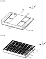
Fig. 2 is a perspective view of thesocket type connectors 1 ofFig. 1 and afirst cap 100 to be attached to thesocket type connectors 1; -
Fig. 3 is a perspective view of theplug type connectors 2 ofFig. 1 and asecond cap 200 to be attached to theplug type connectors 2; -
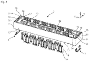
Fig. 4 is an exploded view of thesocket type connector 1 ofFig. 2 ; -
Fig. 5 is an exploded view of theplug type connector 2 ofFig. 3 ; -
Fig. 6 is a perspective view of afirst housing 10 of thesocket type connector 1 ofFig. 4 ; -
Fig. 7 is a perspective view of asecond housing 20 of theplug type connector 2 ofFig. 5 ; -
Fig. 8 is a perspective view of asolder tab terminal 7 of thesocket type connector 1 ofFig. 4 and theplug type connector 2 ofFig. 5 ; -
Fig. 9 is a perspective view ofcontacts 8 of thesocket type connector 1 ofFig. 4 and theplug type connector 2 ofFig. 5 ; -
Fig. 10 is a perspective view of thefirst cap 100 ofFig. 2 as viewed from an opposite side; -
Fig. 11 is a perspective view of thesecond cap 200 ofFig. 3 as viewed from an opposite side; -
Fig. 12A is a line sectional view of a cut surface parallel to the XZ plane ofFig. 1 ; -
Fig. 12B is an enlarged view inside the F frame ofFig. 12A ; -
Fig. 13A is a diagram ofFig. 1 as viewed from the -Z side; -
Fig. 13B is a sectional view taken along line D-D; -
Fig. 13C is an enlarged view inside the E frame ofFig. 13B ; -
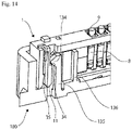
Fig. 14 is a sectional view of a cut surface parallel to the XZ plane, while thefirst cap 100 is attached to thesocket type connector 1; and -
Fig. 15 is a diagram showing each state of expansion during reflow of the three types connectors in this disclosure, (A) shows a state of expansion during reflow of thesocket type connector 1, (B-1) shows a state of expansion during reflow of theplug type connector 2 when the thermal expansion coefficient of thesocket type connector 1 is almost the same as the thermal expansion coefficient of the material of theplug type connector 2; and (B-2) shows a state of expansion during reflow of theplug type connector 2 when the thermal expansion coefficient of the material of theplug type connector 2 is smaller than the thermal expansion coefficient of thesocket type connector 1. - Hereafter, a
socket type connector 1, aplug type connector 2, afirst cap 100, and asecond cap 200 that form a connector set according to one embodiment of the present disclosure will be explained with reference to drawings. A plurality of (four in the example ofFig. 1 )socket type connectors 1 andplug type connectors 2 are arranged side by side, and are respectively mounted on afirst substrate 51 and asecond substrate 52. Thesecond substrate 52 is formed of a material with a lower thermal expansion coefficient than that of thefirst substrate 51. For example, the material of thefirst substrate 51 is FR4 (Flame Retardant Type 4), and the material of thesecond substrate 52 is ceramic. - When
headers 29 of theplug type connectors 2 on thesecond substrate 52 are fitted intoslots 19 of thesocket type connectors 1 on thefirst substrate 51, thecontacts 8 of thesocket type connectors 1 are electronically connected to thecontacts 8 of theplug type connector 2, and high speed differential transmission based on PAM (Pulse Amplitude Modulation) becomes possible. - The
first cap 100 is attached to thesocket type connectors 1 when thesocket type connectors 1 are reflow-mounted on thefirst substrate 51. Thesecond cap 200 is attached to theplug type connectors 2 when theplug type connectors 2 are reflow-mounted on thesecond substrate 52. - In the following description, the fitting direction of the
plug type connector 2 to thesocket type connector 1 is appropriately referred to as the Z direction, the direction orthogonal to the Z direction is appropriately referred to as the X direction, and the direction orthogonal to the Z direction and the X direction is appropriately referred to as the Y direction. In addition, the +Z side may be referred to as an upper side, the -Z side may be referred to as a lower side, the +X side may be referred to as a front side, the -X side may be referred to as a rear side, the +Y side may be referred to as a left side, and the -Y side may be referred to as a right side. - As shown in
Fig. 4 , thesocket type connector 1 has afirst housing 10,solder tab terminals 7 andcontacts 8. As shown inFig. 5 , theplug type connector 2 has asecond housing 20,solder tab terminals 7 andcontacts 8. Thefirst housing 10 of thesocket type connector 1 and thesecond housing 20 of theplug type connector 2 are formed by injecting resin in the X direction which is the longitudinal direction. Thefirst housing 10 of thesocket type connector 1 and thesecond housing 20 of theplug type connector 2 have a rotationally asymmetrical shape. - More specifically, the
first housing 10 of thesocket type connector 1 is provided with twoslots 19. The twoslots 19 extend in the X direction. Thefirst housing 10 has abottom portion 13 that becomes the bottom of thehousing 10,wall portions 11 andwall portions 12 respectively facing each other in the X direction and the Y direction so as to surround theslots 19, and apartition wall 17 separating the twoslots 19 in a frontage surrounded by thewall portions 11 and thewall portions 12. Thewall portions 11 extend in the Y direction, and thewall portions 12 extend in the X direction. In the present disclosure, thewall portions 11 and thewall portions 12 correspond to, for example, the first wall portions and the second wall portions that are defined in claims, respectively. - The end portion of the
partition wall 17 on the -X side is connected to thewall portion 11 on the -X side. The end portion of thepartition wall 17 on the +X side is not connected to thewall portion 11 on the +X side, and agap 18 is formed between the end portion of thepartition wall 17 on the +X side and thewall portion 11 on the +X side. - A
round hole 31 is provided in the middle of thewall portion 11 on the -X side in the Y direction. Along hole 33 is provided in the middle of thewall portion 11 on the +X side in the Y direction. The +X side of thelong hole 33 is open.Rectangular grooves 35 are provided on the +Y side and the -Y side of the holes in thewall portion 11 on the -X side and thewall portion 11 on the +X side. Therectangular grooves 35 are recessed from the upper surfaces of thewall portions 11 toward thebottom portion 13. Holes are perforated at the bottoms of therectangular grooves 35, and thesolder tab terminals 7 are fitted and fixed in the holes. As shown inFig. 8 , thesolder tab terminal 7 has an elongatedsubstrate portion 71 and two projectingpiece portions 72 rising from two end portions of one long side of thesubstrate portion 71. The two projectingpiece portions 72 are fitted into the holes at the bottom of therectangular groove 35 of thefirst housing 10. - As shown in
Fig. 14 , on the lower sides of the inner surfaces of thewall portions 11 on the +X side and the -X side on theslots 19 sides, there are engagingpieces 34 projecting to theslots 19 sides. -
Grooves 36 are provided in the inner surfaces of thewall portions 12 and the side surfaces of thepartition wall 17.Contacts 8 are accommodated in thegrooves 36. As shown inFig. 9 , thecontact 8 has alinear portion 81 extending in one direction, aterminal portion 82 at one end of thelinear portion 81, and afork portion 83 at the other end of thelinear portion 81. Theterminal portion 82 is bent into a doglegged shape. Thefork portion 83 is bifurcated.Solder 9 is caulked and fixed to thefork portion 83. Thecontact 8 is held in thegrooves 36 of thewall portion 12 and thepartition wall 17, and thefork portion 83 of thecontact 8 and thesolder 9 are exposed to the opposite side to thegroove 36 side through the hole in thebottom portion 13. - As shown in
Fig. 2 andFig. 10 , thefirst cap 100 has a box shape with a width in the X direction and the Y direction slightly larger than that of foursocket type connectors 1 arranged side by side. Afirst opening 130 is provided on the -Z side of thefirst cap 100. Thefirst cap 100 has atop plate portion 113 that becomes a ceiling of thefirst cap 100,wall portions 111 andwall portions 112 respectively facing each other in the X direction and the Y direction across thefirst opening 130. - A hooking
spring 135 and aspring accommodation portion 136 are provided at a position corresponding to eachslot 19 of fourfirst housings 10 inside thewall portion 112 on the -X side and thewall portion 112 on the +X side. As shown inFig. 14 , thelower end portion 134 of the hookingspring 135 projects outward in a triangular shape. - A positioning pin is provided at a position corresponding to the
round hole 31 between the adjacentspring accommodation portions 136 inside thewall portion 112 on the -X side. The positioning pin has a shape to be put in theround hole 31. A positioning long pin is provided at a position corresponding to thelong hole 33 between the adjacentspring accommodation portions 136 inside thewall portion 112 on the +X side. The positioning long pin has a shape to be put in thelong hole 33. - The attachment of the
first cap 100 to thesocket type connector 1 and the reflow mounting thereof are performed as follows. First, the foursocket type connectors 1 are arranged in such a manner that the orientation of thegaps 18 of a part of thesocket type connectors 1 and the orientation of thegaps 18 of the remainingsocket type connectors 1 are reversed (for example, thegaps 18 of twosocket type connectors 1 in the middle are on the -X side, and thegaps 18 of twosocket type connectors 1 at both ends are on the +X side). - Next, the
first cap 100 is attached to the foursocket type connectors 1 in such a manner that the positioning pins are inserted into the round holes 31 on the -X side, the positioning long pins are inserted into thelong holes 33 on the +X side, and the hookingsprings 135 are fitted inside thewall portions 11 on the -X side and the +X side. As shown in Fig. 14A and Fig. 14B, when thefirst cap 100 is attached to the foursocket type connectors 1, thelower end portions 134 of the hookingsprings 135 of thefirst cap 100 engage with the engagingpieces 34 of theconnectors 1, and thesocket type connectors 1 are supported from the inside in the X direction by the hookingsprings 135 of thefirst cap 100. - Next, the four
socket type connectors 1 gathered by thefirst cap 100 are placed on a predetermined position of thefirst substrate 51, and are put into a reflow device. The temperature in the device is changed from 20 °C to 260°C to 20°C. When the temperature exceeds 217 °C, thesolder 9 at the tip end portion of thecontact 8 is melted, and when the temperature returns to ordinary temperature, thesolder 9 solidifies. Thecontact 8 of thesocket type connector 1 and the pad of thefirst substrate 51 are connected to each other by the solidification of thesolder 9. After thesocket type connector 1 is attached to thefirst substrate 51, thefirst cap 100 is removed from thesocket type connector 1. - As shown in
Fig. 5 andFig. 7 , thesecond housing 20 of theplug type connector 2 is provided with twoheaders 29. The twoheaders 29 extend in the X direction. The end portions on the -X side, +X side, -Y side, and +Y side of thebottom portion 23 that becomes the bottom of the twoheaders 29 of thesecond housing 20 project outside the portion that supports theheaders 29. Afitting plate portion 48 is provided between the end portions of twoadjacent headers 29 on the -X side in thesecond housing 20. - A
round hole 41 is provided in the middle of the end portion of thebottom portion 23 on the -X side in the Y direction. A second long hole is provided in the middle of the end portion of thebottom portion 23 on the +X side in the Y direction. The +X side of the second long hole is open. Rectangular holes 45 are provided on the +Y side and the -Y side of the holes in the end portions of thebottom portion 23 on the -X side and the +X side.Solder tab terminals 7 are fitted and fixed in the rectangular holes 45. -
Grooves 46 are provided in the side surfaces of the twoheaders 29 on the +Y side and the -Y side.Contacts 8 are accommodated in thegrooves 46. Thecontacts 8 are held in thegrooves 46 of theheaders 29, and thefork portions 83 of thecontacts 8 andsolder 9 are exposed on the opposite side to thegrooves 46 side through holes in thebottom portion 23. - As shown in
Fig. 3 andFig. 11 , thesecond cap 200 has a box shape with a width in the X direction and the Y direction slightly larger than that of fourplug type connectors 2 arranged side by side. Asecond opening 230 is provided on the +Z side of thesecond cap 200. Thesecond cap 200 has atop plate portion 213 that becomes a ceiling of thesecond cap 200,wall portions 211 andwall portions 212 respectively facing each other in the X direction and the Y direction across thesecond opening 230. - There are holding
piece portions 227,which project inside, at positions corresponding to the gaps between theheaders 29 of thesecond housings 20 on the inner side of thewall portion 211 on the -X side. There are holdingpiece portions 229,which project inside, at positions corresponding to the gaps between theheaders 29 of thesecond housings 20 on the inner side of thewall portion 211 on the + X side. - Positioning pins are provided at positions corresponding to the round holes 41 of the
second housings 20 between the adjacentholding piece portions 227 of thewall portion 211 on the -X side. The positioning pin has a shape to be put in theround hole 41. Positioning long pins are provided at positions corresponding to the second long holes of thesecond housings 20 between the adjacentholding piece portions 229 of thewall portion 211 on the +X side. The positioning long pin has a shape to be put in the second long hole. - The attachment of the
second cap 200 to theplug type connectors 2 and the reflow-mounting thereof are performed as follows. First, the fourplug type connectors 2 are arranged in such a manner that the combination of thefitting plate portions 48 on one side and thefitting plate portions 48 on the other side fits the gap of the foursocket type connectors 1. - Next, the
second cap 200 is attached to the fourplug type connectors 2 in such a manner that the positioning pins are inserted into the round holes 41 on the +X side and the positioning long pins are inserted into the second long holes on the -X side. When thesecond cap 200 is attached to the fourplug type connectors 2, the holdingpiece portions 227and 229 of thesecond cap 200 abut against theheaders 29 of theplug type connectors 2, and the foursocket type connectors 1 are supported from the outside in the X direction by the holdingpiece portions 227and 229 of thesecond cap 200. - Next, the four
plug type connectors 2 gathered by thesecond cap 200 are placed on a predetermined position of thesecond substrate 52, and are put into a reflow device. The temperature in the device is changed from 20 °C to 260°C to 20°C. When the temperature exceeds 217 °C, thesolder 9 at the tip end portion of thecontact 8 is melted, and when the temperature returns to ordinary temperature, thesolder 9 solidifies. Thecontact 8 of theplug type connector 2 and the pad of thesecond substrate 52 are connected to each other by the solidification of thesolder 9. After theplug type connector 2 is attached to thesecond substrate 52, thesecond cap 200 is removed from theplug type connector 2. - When the
plug type connector 2 and thesocket type connector 1 are connected in a correct orientation, thefitting plate portion 48 of theplug type connector 2 is fitted to thegap 18 of thesocket type connector 1. When theplug type connector 2 and thesocket type connector 1 are connected in an incorrect orientation, thefitting plate portion 48 of theplug type connector 2 interferes with thepartition wall 17 of thesocket type connector 1. When theplug type connector 2 and thesocket type connector 1 are oriented in opposite directions, thefitting plate portion 48 and thepartition wall 17 interfere with each other, so that reverse insertion ofplug type connector 2 and thesocket type connector 1 is prevented. - As shown in
Fig. 13B and Fig. 13C , when theplug type connector 2 and thesocket type connector 1 are connected in the correct orientation, thecontacts 8 of theplug type connector 2 and thecontacts 8 of thesocket type connector 1 come into contact with each other. Further, as shown inFig. 12A and Fig. 12B , among thecontacts 8 disposed oppositely on both sides of each of theheader 29 and theslot 19, the position of the contact on the -Y side and the position of thecontact 8 on the +Y side are shifted in the X direction by 1/2 contact. The reason why the position of thecontact 8 on the -Y side and the position of thecontact 8 on the +Y side are shifted in the X direction by 1/2 contact is to effectively prevent crosstalk. - Here, the
first cap 100 and thesecond cap 200 are formed of different materials. The thermal expansion coefficient of the material of thesecond cap 200 is smaller than the thermal expansion coefficient of the material of thefirst cap 100. More specifically, when the thermal expansion coefficient of thefirst cap 100 in the Y direction, which is the arranging direction of the foursocket type connectors 1, is α11, the thermal expansion coefficient of thefirst substrate 51 in the Y direction is α10, the thermal expansion coefficient of thesecond cap 200 in the Y direction is α21, and the thermal expansion coefficient of thesecond substrate 52 in the Y direction is α20, α11/α10≈α21/α20. This is to settle the difference between the mounting position of thecontact 8 of thesocket type connector 1 on thefirst substrate 51 and the mounting position of thecontact 8 of theplug type connector 2 on thesecond substrate 52 to be less than 0.15 mm. - The reason why the mounting position error of the
socket type connector 1 and theplug type connector 2 can be reduced by setting the thermal expansion coefficient of thesecond cap 200 smaller than the thermal expansion coefficient of thefirst cap 100 is as follows. - As shown in
Fig. 15 ((A) and (B-1)), in the reflow mounting, thefirst cap 100, thefirst housing 10, and thefirst substrate 51, as well as thesecond cap 200, thesecond housing 20, and thesecond substrate 52 expand in the Y direction when the temperature in the reflow device becomes high, and contract when the temperature returns to ordinary temperature. - With the expansion of the
first cap 100, the distance between theadjacent contacts 8 in thefirst housing 10 of thesocket type connector 1 widens, and the positions of thecontacts 8 of thesocket type connector 1 at the time when temperature exceeds the melting temperature of thesolder 9 and reaches 260°C become the mounting positions of thecontacts 8 on thefirst substrate 51. Similarly, the positions of thecontacts 8 of theplug type connector 2 at the time when the temperature reaches 260°C become the mounting positions of thecontacts 8 on thesecond substrate 52. - As described above, ceramic, which is the material of the
second substrate 52, has a smaller thermal expansion coefficient than that of FR4, which is the material of thefirst substrate 51. For this reason, assuming that thefirst cap 100 and thesecond cap 200 are materials with almost the same thermal expansion coefficient as that of thefirst substrate 51, thefirst substrate 51 contracts while returning from 260°C to 20°C, and the interval between thecontacts 8 of thesocket type connector 1 also returns to the original interval. On the other hand, thesecond substrate 52 hardly contracts, and the interval between thecontacts 8 of theplug type connector 2 remains widened by expansion. As a result, the mounting position error of thesocket type connector 1 and theplug type connector 2 becomes large. - In contrast, as shown in
Fig. 15 (B-2), when the thermal expansion coefficient of thesecond cap 200 is made smaller than the thermal expansion coefficient of thefirst cap 100, the interval of thecontacts 8 of theplug type connector 2 at the time of reaching 260 °C becomes smaller than that in the state where the thermal expansion coefficients are the same. Accordingly, the mounting position error of thesocket type connector 1 and theplug type connector 2 at the time when the temperature returns from 260 °C to 20 °C becomes smaller. - The details of the present embodiment have been described above. The connector set according to the present embodiment includes: a
socket type connector 1 as a first connector; afirst cap 100 to be attached to thesocket type connector 1 when thesocket type connector 1 is reflow-mounted on thefirst substrate 51; aplug type connector 2 as a second connector; and asecond cap 200 to be attached to theplug type connector 2 when theplug type connector 2 is reflow-mounted on thesecond substrate 52, wherein thesecond substrate 52 is formed of a material with a smaller thermal expansion coefficient than that of thefirst substrate 51, and thesecond cap 200 is formed of a material with a smaller thermal expansion coefficient than that of thefirst cap 100. Accordingly, it is possible to absorb the difference between the thermal expansion coefficient of the material of the circuit board on which thesocket type connector 1 is mounted and the thermal expansion coefficient of the material of the circuit board on which theplug type connector 2 is mounted, and reduce the mounting position error. - Further, the connector according to the present embodiment includes a plurality of
socket type connectors 1 to be mounted on afirst substrate 51, and a plurality ofplug type connectors 2 to be mounted on asecond substrate 52. Thesocket type connector 1 includes afirst housing 10 with aslot 19, and a plurality ofcontact 8 arranged in theslot 19. Theplug type connector 2 includes asecond housing 20 with aheader 29 to be fitted into theslot 19, and a plurality ofcontacts 8 arranged in theheader 29. Then, thefirst housing 10 of thesocket type connector 1 and thesecond housing 20 of theplug type connector 2 have a rotationally asymmetrical shape as viewed in a fitting direction. Thus, it is possible to provide a connector that is unlikely to be reversely inserted. - Further, in the present embodiment, the
slots 19 of thesocket type connector 1 and theheaders 29 of theplug type connector 2 are in two rows. For this reason, compared with one row in the conventional connector, it is possible to make it difficult to apply stress to thesolder 9. - Although the embodiments of the present disclosure have been described above, the following modifications may be added to this embodiment.
- (1)In the above embodiment, the number of the connectors gathered by the cap and mounted on the substrate may be two to three or four or more.
- (2) In the above embodiment, there may be one or three or more rows of
slots 19 in onesocket type connector 1, and there may be one or three or more rows ofheaders 29 in oneplug type connector 2. -
- 1 socket type connector
- 2 plug type connector
- 7 solder tab terminal
- 8 contact
- 10 first housing
- 11 wall portion
- 12 wall portion
- 13 bottom portion
- 17 partition wall
- 18 gap
- 19 slot
- 20 second housing
- 23 bottom portion
- 29 header
- 31 round hole
- 33 long hole
- 34 engaging piece
- 35 rectangular groove
- 36 groove
- 41 round hole
- 45 rectangular hole
- 46 groove
- 48 fitting plate portion
- 51 first substrate
- 52 second substrate
- 71 substrate portion
- 72 projecting piece portion
- 81 linear portion
- 82 terminal portion
- 83 fork portion
- 100 first cap
- 111 wall portion
- 112 wall portion
- 113 top plate portion
- 130 first opening
- 134 lower end portion
- 135 spring
- 136 spring accommodation portion
- 200 second cap
- 211 wall portion
- 212 wall portion
- 213 top plate portion
- 227 holding piece portion
- 229 holding piece portion
- 230 second opening
Claims (6)
- A connector comprising a plurality of socket type connectors (1) to be mounted on an external first substrate and a plurality of plug type connectors (2) to be mounted on an external second substrate, and electrically connecting the first substrate and the second substrate, wherein
the socket type connector (1) comprises:a housing (10) with a slot (19); anda plurality of contacts (8) arranged in the slot (19),the plug type connector (2) comprises:a housing (20) with a header (29) to be fitted in the slot (19); anda plurality of contacts (8) arranged in the header (29),the housing (10) of the socket type connector (1) and the housing (20) of the plug type connector (2) comprises a rotationally asymmetrical shape as viewed from a fitting direction(Z). - The connector according to claim 1, whereinthe housing (10) of the socket type connector (1) comprises a bottom portion (13), two first wall portions (11) facing each other in a first direction (X) orthogonal to the fitting direction (Z), and two second wall portions (12) facing each other in a second direction (Y) orthogonal to the fitting direction (Z) and the first direction (X), so as to surround the slot (19),the slot (19) is separated into a plurality of slots (19) by a partition wall (17) extending along the first direction (X), one end portion of the partition wall (17) is connected to one first wall portion (11) of the two first wall portions (11) on both sides of the first direction (X), the other end portion of the partition wall (11) is not connected to the other first wall portion (11), and a gap (18) is formed between the other end portion of the partition wall (17) and the other first wall portion (11).
- The connector according to claim 2, wherein
the housing (20) of the plug type connector (20) comprises a plurality of headers (29), the plurality of headers (29) extend in the first direction (X), a fitting plate portion (48) to be fitted in the gap (18) is provided between the adjacent one end portions of the plurality of headers (29) in the first direction (X). - The connector according to claim 3, whereina part of socket type connectors (1) of the plurality of socket type connectors (1) and the remaining socket type connectors (1) are mounted on the first external substrate with the gaps (18) oriented in opposite directions,plug type connectors (2) of the plurality of plug type connectors (2) to be fitted with the part of socket type connectors (1) and the remaining plug type connectors (2) are mounted on the second external substrate with the fitting plate portions (48) oriented in opposite directions.
- The connector according to claim 1, whereina number of the slots (19) in one socket type connector (1) is two,a number of the headers (29) in one plug type connector (2) is two.
- The connector according to claim 1, wherein
among the contacts (8) respectively disposed on both sides of the slots (19) and the headers (29), a position of the contact (8) on one side and a position of the contact (8) on the other side are shifted by 1/2 contact.
Applications Claiming Priority (1)
| Application Number | Priority Date | Filing Date | Title |
|---|---|---|---|
| CN202011549509.3A CN114678709B (en) | 2020-12-24 | 2020-12-24 | Connector and connector kit |
Publications (2)
| Publication Number | Publication Date |
|---|---|
| EP4020719A1 true EP4020719A1 (en) | 2022-06-29 |
| EP4020719B1 EP4020719B1 (en) | 2026-03-04 |
Family
ID=79287979
Family Applications (1)
| Application Number | Title | Priority Date | Filing Date |
|---|---|---|---|
| EP21217701.8A Active EP4020719B1 (en) | 2020-12-24 | 2021-12-24 | Connector |
Country Status (3)
| Country | Link |
|---|---|
| US (1) | US11949179B2 (en) |
| EP (1) | EP4020719B1 (en) |
| CN (1) | CN114678709B (en) |
Families Citing this family (2)
| Publication number | Priority date | Publication date | Assignee | Title |
|---|---|---|---|---|
| CN114744423A (en) * | 2020-12-24 | 2022-07-12 | 山一电机株式会社 | Connector Kits and Covers |
| CN114678709B (en) * | 2020-12-24 | 2025-07-25 | 山一电机株式会社 | Connector and connector kit |
Citations (5)
| Publication number | Priority date | Publication date | Assignee | Title |
|---|---|---|---|---|
| WO1999009619A2 (en) * | 1997-08-14 | 1999-02-25 | The Panda Project | Electrical connector having staggered hold-down tabs |
| US20050287839A1 (en) * | 2004-06-28 | 2005-12-29 | Hon Hai Precision Ind. Co., Ltd. | Electrical connector with improved signal transmission effect |
| JP2018113146A (en) | 2017-01-11 | 2018-07-19 | 日本圧着端子製造株式会社 | Board to Board Connector |
| US20190131731A1 (en) * | 2017-10-27 | 2019-05-02 | Advanced-Connectek Inc. | Board-to-board plug electrical plug connector, board-to-board electrical receptacle connector, and board-to-board electrical connector assembly |
| WO2020010245A1 (en) * | 2018-07-06 | 2020-01-09 | Samtec, Inc. | Connector with top- and bottom-stitched contacts |
Family Cites Families (36)
| Publication number | Priority date | Publication date | Assignee | Title |
|---|---|---|---|---|
| US4275944A (en) * | 1979-07-09 | 1981-06-30 | Sochor Jerzy R | Miniature connector receptacles employing contacts with bowed tines and parallel mounting arms |
| US5219294A (en) * | 1991-02-20 | 1993-06-15 | Amp Incorporated | Electrical docking connector |
| WO1994002975A1 (en) * | 1992-07-17 | 1994-02-03 | Berg Technology, Inc. | Flat back card connector |
| US6024584A (en) * | 1996-10-10 | 2000-02-15 | Berg Technology, Inc. | High density connector |
| TW406454B (en) * | 1996-10-10 | 2000-09-21 | Berg Tech Inc | High density connector and method of manufacture |
| US6981883B2 (en) * | 2001-11-14 | 2006-01-03 | Fci Americas Technology, Inc. | Impedance control in electrical connectors |
| US6994569B2 (en) * | 2001-11-14 | 2006-02-07 | Fci America Technology, Inc. | Electrical connectors having contacts that may be selectively designated as either signal or ground contacts |
| KR100545000B1 (en) * | 2003-04-09 | 2006-01-24 | 대은전자 주식회사 | ID connector |
| JP4425732B2 (en) * | 2004-07-21 | 2010-03-03 | 株式会社オートネットワーク技術研究所 | Board mounted connector |
| CN2812293Y (en) * | 2005-06-23 | 2006-08-30 | 资重兴 | Memory module with its chips being connected by holddown piece and conducting terminals |
| US7497736B2 (en) * | 2006-12-19 | 2009-03-03 | Fci Americas Technology, Inc. | Shieldless, high-speed, low-cross-talk electrical connector |
| CN201204309Y (en) * | 2008-03-25 | 2009-03-04 | 富士康(昆山)电脑接插件有限公司 | electrical connector |
| US7918668B1 (en) * | 2010-02-22 | 2011-04-05 | Tyco Electronics Corporation | Socket connector assembly with conductive posts |
| JP5634095B2 (en) * | 2010-03-31 | 2014-12-03 | ホシデン株式会社 | Connector and printed circuit board foot pattern for connector |
| CN102315534B (en) * | 2010-07-08 | 2014-08-20 | 泰科电子(上海)有限公司 | Electric connector |
| US8353726B2 (en) * | 2010-11-03 | 2013-01-15 | Hon Hai Precision Inc. Co., Ltd. | Electrical connector with grounding bars therein to reduce cross talking |
| US8425236B2 (en) * | 2011-05-16 | 2013-04-23 | International Business Machines Corporation | Tall mezzanine connector |
| JP5908225B2 (en) * | 2011-07-06 | 2016-04-26 | 第一電子工業株式会社 | Electrical connector |
| JP5685216B2 (en) * | 2012-03-29 | 2015-03-18 | ヒロセ電機株式会社 | Electrical connector assembly and receptacle connector |
| US9543703B2 (en) * | 2012-07-11 | 2017-01-10 | Fci Americas Technology Llc | Electrical connector with reduced stack height |
| JP5790950B2 (en) * | 2013-04-02 | 2015-10-07 | Smk株式会社 | Board connector |
| CN104518310A (en) * | 2013-09-27 | 2015-04-15 | 阿尔卑斯电气株式会社 | Connector unit |
| JP6188638B2 (en) * | 2014-06-10 | 2017-08-30 | ヒロセ電機株式会社 | Receptacle connector, receptacle connector with circuit board and plug connector |
| JP2016035831A (en) * | 2014-08-01 | 2016-03-17 | パナソニックIpマネジメント株式会社 | connector |
| US10396481B2 (en) * | 2014-10-23 | 2019-08-27 | Fci Usa Llc | Mezzanine electrical connector |
| TWI581528B (en) * | 2014-12-12 | 2017-05-01 | 連展科技股份有限公司 | Socket electrical connector |
| CN106207546A (en) * | 2016-06-23 | 2016-12-07 | 中航光电科技股份有限公司 | A kind of signal mode and use the adapter of this signal mode |
| CN207705421U (en) * | 2017-12-19 | 2018-08-07 | 华为技术有限公司 | A kind of chip pocket and network system |
| US10511127B2 (en) * | 2018-03-20 | 2019-12-17 | Microsoft Technology Licensing, Llc | High-speed electronic connector |
| JP7164374B2 (en) * | 2018-09-25 | 2022-11-01 | ヒロセ電機株式会社 | ELECTRICAL CONNECTOR FOR CIRCUIT BOARD AND METHOD FOR MANUFACTURING ELECTRICAL CONNECTOR FOR CIRCUIT BOARD |
| TW202534957A (en) * | 2020-01-27 | 2025-09-01 | 美商Fci美國有限責任公司 | High speed, high density direct mate orthogonal connector |
| CN212209927U (en) * | 2020-06-02 | 2020-12-22 | 山一电机株式会社 | Socket and IC package |
| CN114678709B (en) * | 2020-12-24 | 2025-07-25 | 山一电机株式会社 | Connector and connector kit |
| CN214013206U (en) * | 2020-12-24 | 2021-08-20 | 山一电机株式会社 | Connectors and Connector Kits |
| CN114744424B (en) * | 2020-12-24 | 2025-06-06 | 山一电机株式会社 | Connector Kits and Connectors |
| CN114744423A (en) * | 2020-12-24 | 2022-07-12 | 山一电机株式会社 | Connector Kits and Covers |
-
2020
- 2020-12-24 CN CN202011549509.3A patent/CN114678709B/en active Active
-
2021
- 2021-12-22 US US17/559,270 patent/US11949179B2/en active Active
- 2021-12-24 EP EP21217701.8A patent/EP4020719B1/en active Active
Patent Citations (5)
| Publication number | Priority date | Publication date | Assignee | Title |
|---|---|---|---|---|
| WO1999009619A2 (en) * | 1997-08-14 | 1999-02-25 | The Panda Project | Electrical connector having staggered hold-down tabs |
| US20050287839A1 (en) * | 2004-06-28 | 2005-12-29 | Hon Hai Precision Ind. Co., Ltd. | Electrical connector with improved signal transmission effect |
| JP2018113146A (en) | 2017-01-11 | 2018-07-19 | 日本圧着端子製造株式会社 | Board to Board Connector |
| US20190131731A1 (en) * | 2017-10-27 | 2019-05-02 | Advanced-Connectek Inc. | Board-to-board plug electrical plug connector, board-to-board electrical receptacle connector, and board-to-board electrical connector assembly |
| WO2020010245A1 (en) * | 2018-07-06 | 2020-01-09 | Samtec, Inc. | Connector with top- and bottom-stitched contacts |
Also Published As
| Publication number | Publication date |
|---|---|
| US20220209443A1 (en) | 2022-06-30 |
| CN114678709B (en) | 2025-07-25 |
| EP4020719B1 (en) | 2026-03-04 |
| US11949179B2 (en) | 2024-04-02 |
| CN114678709A (en) | 2022-06-28 |
Similar Documents
| Publication | Publication Date | Title |
|---|---|---|
| EP4037109B1 (en) | Connector set and cap | |
| US6875031B1 (en) | Electrical connector with circuit board module | |
| US9502815B2 (en) | Electrical connector | |
| JP4592462B2 (en) | Board connector | |
| EP4044377B1 (en) | Connector set and connector | |
| CN106921056A (en) | Connector and connector assembly | |
| CN101483285A (en) | Electric connection block | |
| JP2021174770A (en) | Board-side connector and connector assembly | |
| US11949179B2 (en) | Connector and connector set | |
| KR101452626B1 (en) | Connector assembly for perpendicularly connecting two substrates | |
| JP4102747B2 (en) | connector | |
| CN214013206U (en) | Connectors and Connector Kits | |
| KR20040080996A (en) | Electrical connector | |
| JP4659692B2 (en) | Floating connector | |
| CN213546603U (en) | Connector kit and sealing cover | |
| TW202312601A (en) | Connector characterized by maintaining an electrically stable connection during or after the connection to the connected conductor on the corresponding side even if the situation of the position deviation of a connected conductor on the corresponding side occurs | |
| CN213717097U (en) | Connector Kits and Connectors | |
| JP7572639B2 (en) | connector | |
| US10658776B2 (en) | Right-angle electrical connector | |
| JP7839041B2 (en) | Electrical connectors, electrical connector assemblies, units, and unit assemblies | |
| JP7485988B2 (en) | connector | |
| JP2012156021A (en) | Floating connector | |
| US12494602B2 (en) | Combo connector | |
| JP2024100320A (en) | Sheet-shaped conductive path | |
| CN114447644A (en) | Electric connector for circuit board and electric connector with circuit board |
Legal Events
| Date | Code | Title | Description |
|---|---|---|---|
| PUAI | Public reference made under article 153(3) epc to a published international application that has entered the european phase |
Free format text: ORIGINAL CODE: 0009012 |
|
| STAA | Information on the status of an ep patent application or granted ep patent |
Free format text: STATUS: THE APPLICATION HAS BEEN PUBLISHED |
|
| AK | Designated contracting states |
Kind code of ref document: A1 Designated state(s): AL AT BE BG CH CY CZ DE DK EE ES FI FR GB GR HR HU IE IS IT LI LT LU LV MC MK MT NL NO PL PT RO RS SE SI SK SM TR |
|
| STAA | Information on the status of an ep patent application or granted ep patent |
Free format text: STATUS: REQUEST FOR EXAMINATION WAS MADE |
|
| 17P | Request for examination filed |
Effective date: 20221213 |
|
| RBV | Designated contracting states (corrected) |
Designated state(s): AL AT BE BG CH CY CZ DE DK EE ES FI FR GB GR HR HU IE IS IT LI LT LU LV MC MK MT NL NO PL PT RO RS SE SI SK SM TR |
|
| STAA | Information on the status of an ep patent application or granted ep patent |
Free format text: STATUS: EXAMINATION IS IN PROGRESS |
|
| 17Q | First examination report despatched |
Effective date: 20240510 |
|
| GRAP | Despatch of communication of intention to grant a patent |
Free format text: ORIGINAL CODE: EPIDOSNIGR1 |
|
| STAA | Information on the status of an ep patent application or granted ep patent |
Free format text: STATUS: GRANT OF PATENT IS INTENDED |
|
| RIC1 | Information provided on ipc code assigned before grant |
Ipc: H01R 12/71 20110101AFI20251124BHEP Ipc: H01R 12/73 20110101ALI20251124BHEP Ipc: H01R 13/64 20060101ALI20251124BHEP Ipc: H01R 13/6461 20110101ALN20251124BHEP Ipc: H01R 43/02 20060101ALN20251124BHEP |
|
| INTG | Intention to grant announced |
Effective date: 20251204 |
|
| GRAS | Grant fee paid |
Free format text: ORIGINAL CODE: EPIDOSNIGR3 |
|
| GRAA | (expected) grant |
Free format text: ORIGINAL CODE: 0009210 |
|
| STAA | Information on the status of an ep patent application or granted ep patent |
Free format text: STATUS: THE PATENT HAS BEEN GRANTED |
|
| AK | Designated contracting states |
Kind code of ref document: B1 Designated state(s): AL AT BE BG CH CY CZ DE DK EE ES FI FR GB GR HR HU IE IS IT LI LT LU LV MC MK MT NL NO PL PT RO RS SE SI SK SM TR |
|
| REG | Reference to a national code |
Ref country code: CH Ref legal event code: F10 Free format text: ST27 STATUS EVENT CODE: U-0-0-F10-F00 (AS PROVIDED BY THE NATIONAL OFFICE) Effective date: 20260304 Ref country code: GB Ref legal event code: FG4D |
|
| REG | Reference to a national code |
Ref country code: IE Ref legal event code: FG4D |
|
| REG | Reference to a national code |
Ref country code: DE Ref legal event code: R096 Ref document number: 602021049136 Country of ref document: DE |