EP4020475A1 - Memory module suitable for performing computing functions - Google Patents
Memory module suitable for performing computing functions Download PDFInfo
- Publication number
- EP4020475A1 EP4020475A1 EP21216400.8A EP21216400A EP4020475A1 EP 4020475 A1 EP4020475 A1 EP 4020475A1 EP 21216400 A EP21216400 A EP 21216400A EP 4020475 A1 EP4020475 A1 EP 4020475A1
- Authority
- EP
- European Patent Office
- Prior art keywords
- circuit
- memory
- data
- processor
- elementary
- Prior art date
- Legal status (The legal status is an assumption and is not a legal conclusion. Google has not performed a legal analysis and makes no representation as to the accuracy of the status listed.)
- Pending
Links
Images


Classifications
-
- G—PHYSICS
- G11—INFORMATION STORAGE
- G11C—STATIC STORES
- G11C7/00—Arrangements for writing information into, or reading information out from, a digital store
- G11C7/10—Input/output [I/O] data interface arrangements, e.g. I/O data control circuits, I/O data buffers
- G11C7/1006—Data managing, e.g. manipulating data before writing or reading out, data bus switches or control circuits therefor
-
- G—PHYSICS
- G11—INFORMATION STORAGE
- G11C—STATIC STORES
- G11C7/00—Arrangements for writing information into, or reading information out from, a digital store
- G11C7/10—Input/output [I/O] data interface arrangements, e.g. I/O data control circuits, I/O data buffers
- G11C7/1078—Data input circuits, e.g. write amplifiers, data input buffers, data input registers, data input level conversion circuits
- G11C7/1096—Write circuits, e.g. I/O line write drivers
-
- G—PHYSICS
- G06—COMPUTING; CALCULATING OR COUNTING
- G06F—ELECTRIC DIGITAL DATA PROCESSING
- G06F13/00—Interconnection of, or transfer of information or other signals between, memories, input/output devices or central processing units
- G06F13/14—Handling requests for interconnection or transfer
- G06F13/16—Handling requests for interconnection or transfer for access to memory bus
- G06F13/1605—Handling requests for interconnection or transfer for access to memory bus based on arbitration
-
- G—PHYSICS
- G06—COMPUTING; CALCULATING OR COUNTING
- G06F—ELECTRIC DIGITAL DATA PROCESSING
- G06F13/00—Interconnection of, or transfer of information or other signals between, memories, input/output devices or central processing units
- G06F13/14—Handling requests for interconnection or transfer
- G06F13/16—Handling requests for interconnection or transfer for access to memory bus
- G06F13/1668—Details of memory controller
-
- G—PHYSICS
- G11—INFORMATION STORAGE
- G11C—STATIC STORES
- G11C7/00—Arrangements for writing information into, or reading information out from, a digital store
- G11C7/10—Input/output [I/O] data interface arrangements, e.g. I/O data control circuits, I/O data buffers
- G11C7/1015—Read-write modes for single port memories, i.e. having either a random port or a serial port
- G11C7/1039—Read-write modes for single port memories, i.e. having either a random port or a serial port using pipelining techniques, i.e. using latches between functional memory parts, e.g. row/column decoders, I/O buffers, sense amplifiers
-
- G—PHYSICS
- G11—INFORMATION STORAGE
- G11C—STATIC STORES
- G11C7/00—Arrangements for writing information into, or reading information out from, a digital store
- G11C7/10—Input/output [I/O] data interface arrangements, e.g. I/O data control circuits, I/O data buffers
- G11C7/1051—Data output circuits, e.g. read-out amplifiers, data output buffers, data output registers, data output level conversion circuits
- G11C7/1063—Control signal output circuits, e.g. status or busy flags, feedback command signals
-
- G—PHYSICS
- G11—INFORMATION STORAGE
- G11C—STATIC STORES
- G11C7/00—Arrangements for writing information into, or reading information out from, a digital store
- G11C7/10—Input/output [I/O] data interface arrangements, e.g. I/O data control circuits, I/O data buffers
- G11C7/1051—Data output circuits, e.g. read-out amplifiers, data output buffers, data output registers, data output level conversion circuits
- G11C7/1069—I/O lines read out arrangements
-
- G—PHYSICS
- G11—INFORMATION STORAGE
- G11C—STATIC STORES
- G11C7/00—Arrangements for writing information into, or reading information out from, a digital store
- G11C7/10—Input/output [I/O] data interface arrangements, e.g. I/O data control circuits, I/O data buffers
- G11C7/1075—Input/output [I/O] data interface arrangements, e.g. I/O data control circuits, I/O data buffers for multiport memories each having random access ports and serial ports, e.g. video RAM
-
- G—PHYSICS
- G11—INFORMATION STORAGE
- G11C—STATIC STORES
- G11C7/00—Arrangements for writing information into, or reading information out from, a digital store
- G11C7/10—Input/output [I/O] data interface arrangements, e.g. I/O data control circuits, I/O data buffers
- G11C7/1078—Data input circuits, e.g. write amplifiers, data input buffers, data input registers, data input level conversion circuits
- G11C7/109—Control signal input circuits
Definitions
- the present description generally relates to the field of memory circuits, and is more particularly aimed at the field of memory circuits adapted to implement calculation operations.
- Memory circuits adapted to implement calculation operations or “intelligent” memory circuits (often called “smart memory”) have already been proposed. Such circuits are for example intended to cooperate with a processor, so as to relieve the processor of certain calculation tasks.
- the direct transfer circuit comprises a buffer circuit adapted to temporarily store data transiting from or to the memory circuit.
- the device comprises a distribution circuit connected to said connection port of the device to the processor, the distribution circuit receiving the first and second instructions from the processor and being adapted to transmit the first instructions to the first control circuit and the second instructions to the direct transfer circuit, the distribution circuit using address information present in the instruction to carry out this distribution.
- the internal link has a data width equal to the size of the largest data vector that can be read at once in said memory circuit.
- the internal link has a data width at least twice greater than the data width of the connection port of the device to the processor.
- the direct transfer circuit is connected to a connection port of the module to a memory system bus external to the device.
- connection port of the device to the memory system bus has a data width greater than the data width of the connection port of the device to the processor.
- the buffer circuit of the direct transfer circuit is suitable for temporarily storing data transiting between said memory circuit and an external memory circuit connected to said memory system bus.
- the direct transfer circuit comprises configuration registers storing the second instructions received from the processor.
- the direct transfer circuit further comprises a second control circuit adapted to read and write in the configuration registers, to exchange control data with the arbitration circuit, and to control data transfers via the buffer circuit.
- said memory circuit comprises a plurality of memory circuits adapted to implement calculation operations, said memory circuits being arranged in a matrix according to rows and columns.
- the memory circuit array is reconfigurable so as to adjust the dimension of the data vectors in the direction of the rows.
- One embodiment provides a system comprising a memory device, a processor adapted to transmit the first and second instructions to the memory device, a memory system bus connected to the direct transfer circuit of the memory device, and an external memory circuit connected to the memory system bus , in which the direct transfer circuit is adapted to transfer data directly between the memory circuit of the device and the external memory circuit via the memory system bus, without going through the processor.
- the figure 1 schematically represents an example of a memory circuit 101 (CSRAM) adapted to implement calculation operations.
- Circuit 101 comprises a matrix 103 (SRAM_ARRAY) of elementary storage cells, for example SRAM (Static Random Access Memory) cells.
- SRAM_ARRAY matrix 103 of elementary storage cells
- the matrix 103 comprises M rows and N columns of elementary storage cells 105, with M and N integers greater than or equal to 2.
- the matrix 103 is similar to the matrices described in the patent application EP3252774 previously filed by the applicant.
- the memory circuit 101 further comprises a row selection circuit 107 (RS) adapted to select a single row of the matrix 103 to carry out a conventional read or write operation.
- the row selection circuit 107 can also be adapted to simultaneously select several rows of the matrix 103 in read mode, so as to implement, on the conductive column output tracks of the matrix, basic logic operations having as operands of the data stored in the selected rows.
- the memory circuit 101 can also comprise a calculation circuit 109 (ALU) adapted to implement additional calculation operations from the signals read on the conductive column output tracks of the matrix 103 and/or to rewrite directly in the matrix 103 the result of a calculation operation, without going through external connection terminals of the memory circuit 101.
- ALU calculation circuit 109
- the memory circuit 101 further comprises an input/output circuit 111 (I/O) connecting the columns of the matrix to connection terminals outside the memory circuit, for example to an input/output port of data (not detailed on the figure 1 ) of the memory circuit.
- I/O input/output circuit 111
- the memory circuit of the figure 1 further comprises a control circuit 113 (FSM) connected to circuits 107, 109 and 111.
- Circuit 113 is suitable for decoding and controlling the execution of read, write and/or calculation instructions transmitted by a external control circuit (not shown), for example a processor.
- the picture 2 schematically represents an example of a system comprising a memory module 200 adapted to implement calculation operations according to one embodiment.
- the 200 memory module of the picture 2 comprises a memory circuit 201 (CSRAM) adapted to implement calculation operations.
- CSRAM memory circuit 201
- the memory circuit 201 can be a memory circuit of the IMC type (from the English “In Memory Computing” - calculation in memory), that is to say in which calculations are implemented directly within the matrix of elementary cells of the memory circuit, for example as described in relation to the figure 1 or in the patent application EP3252774 aforementioned. More generally, the memory circuit 201 can be any memory circuit adapted to implement calculation operations, for example an NMC type circuit (from the English “Near Memory Computing” - calculation close to the memory), it that is to say in which the calculations are not carried out directly within the matrix of elementary cells of the memory circuit, but in calculation circuits integrated in the immediate periphery of the matrix of elementary cells.
- the system of figure 2 includes a processor 231 (CPU). More generally, the processor 231 can be replaced by any circuit suitable for generating a flow of control instructions.
- the system of picture 2 further comprises an instruction memory 235 (IM) directly connected to the processor 231 via a link 237.
- the processor 231 and the instruction memory 235 are also connected to the same system bus 239 (CDB) , also called processor system bus or processor data bus or CPU data bus.
- CDB system bus or processor data bus or CPU data bus.
- the bus 239 can be a bus of the type conventionally used to exchange data between a processor and peripherals, for example memory circuits, of a data processing system.
- Bus 239 may in particular comprise a data bus, an address bus and/or a control bus.
- the bus 239 can be implemented by means of a network-on-chip type distributed interconnection system.
- the module 200 further comprises a circuit 203 (DIMA) for direct access to the circuit 201.
- the circuit 203 is directly connected to the memory circuit 201, via a link of data transfer 204 internal to the module 200.
- the circuit 203 is also directly connected to a data transfer system bus 251 (MSB), also called memory system bus ("memory system bus" in English) external to the module 200, by via a link 241.
- MSB data transfer system bus
- memory system bus 251 is not directly connected to the processor 231.
- the bus 251 is a bus specifically dedicated to the direct transfer (i.e.
- the bus 251 can in particular comprise a bus of data, a bu s of addresses and/or a control bus.
- the bus 251 can be implemented by means of a network-on-chip type distributed interconnection system.
- system memory bus 251 and the system bus 239 can advantageously be connected to each other by different interface circuits as is known to those skilled in the art.
- system bus 239 and memory system bus 251 may be a single and same bus, although this is not the preferred embodiment.
- the system bus 239 is often small for data and putting the two buses in common would undoubtedly have the consequence of having a small size bus 251, and moreover of increasing the necessary throughput on the common bus. which could in practice result in a saturation of the bus, and in turn a reduction in the data exchange rate compared to a configuration with two buses.
- memory system bus 251 is wider than processor system bus 239.
- Data transfer link 204 preferably has a width equal to the size of the largest data vector that can be read from the memory circuit at one time. 201, for example equal to the size of a row of read circuits present at the foot of the columns in the matrix of elementary storage cells of the memory circuit 201. In the case where there is no multiplexing at the foot of the column , the size of this largest data vector can be equal to N bits if we consider the example of the figure 1 . If there is multiplexing at the bottom of the column, then the size of this largest vector will be reduced by the multiplexing factor relative to this number N of bits present in a row.
- link 204 may have a width equal to a sub-multiple of the size of the largest data vector that can be read at one time from memory circuit 201.
- Bus 251 may have a width equal to the width of the link 204.
- the width of the bus 251 may be a sub-multiple of the width of the link 204.
- the width of the link 204 is preferably greater than the width of an input port/ output of the processor 231. It will be noted that by width of a bus, of a port or of a link, we mean here the width of the data which can transit in parallel on the bus, the port or the link (independently of possible additional address and/or control signals).
- the direct access circuit 203 is suitable for transferring data directly, that is to say without passing these data through the processor 231, between the memory circuit 201 and the memory system bus 251.
- the system further comprises a memory circuit 253 (MM) external to the module 200.
- the memory circuit 253 is connected to the memory system bus 251 via a link 255.
- the direct access circuit 203 makes it possible to transfer of the data directly, that is to say without passing these data through the processor 231, between the memory circuit 201 of the module 200 and the external memory circuit 253. More generally, the direct access circuit 203 makes it possible to transfer data directly, that is to say without passing these data through the processor 231, between the memory circuit 201 of the module 200 and any peripheral circuit connected to the memory system bus 251.
- the memory circuit 253 can be an SRAM type memory, an NVM type memory (from the English “Non Volatil Memory” - non-volatile memory), a DRAM type memory (from the English “Dynamic Random Access Memory” - dynamic access memory random), a Flash type memory, or yet another memory circuit adapted to implement calculation operations.
- the different components of the module 200 can be integrated into the same integrated circuit chip.
- the memory circuit 253 can be integrated into this same chip, or external to this chip.
- the module 200 further comprises a control circuit 205 (PC for Pipeline Controller) adapted to schedule the accesses to the memory circuit 201 required by the processor 231.
- the circuit 205 is adapted to decode the instructions received from the processor 231 and to break down, if necessary, each instruction received into a sequence of several sub-operations also called elementary operations.
- elementary operation is meant a read, write or calculation operation in the memory 201.
- a calculation operation may possibly consist in actuating only a calculation unit attached to the memory matrix (in the case for example of a NMC-type memory).
- a calculation operation can also consist in carrying out a read operation of one or more rows with actuation of calculation means placed at the bottom of the column (in the case for example of an IMC type memory).
- an elementary operation can be performed in a memory access cycle 201, as is for example described in the patent application French N°20/08272 filed on August 4, 2020 by the applicant in relation to Figures 4A, 4B.
- the instructions sent by the processor may be simple instructions corresponding to a single write or read request in the memory without calculation operations, or may be complex instructions which may in practice require the execution of several elementary read operations, writing or calculation.
- circuit 205 will break down an instruction received into a sequence of several elementary operations only when it receives a complex instruction (or “smart instruction”).
- the memory 201 can, by virtue of its structure, carry out several elementary operations simultaneously, it is then possible to parallelize certain elementary operations.
- parallelized elementary operations can correspond to different simple or complex instructions.
- the circuit 205 can in this case include a device for analyzing the sequences of operations corresponding to the successive instructions, to insert if necessary one or more wait cycles in a sequence of elementary operations corresponding to an instruction, when a potential conflict is detected.
- the 200 module of the picture 2 further comprises a circuit 207 (AD) for distributing requests from the processor 231.
- the circuit 207 is connected to the processor 231 via a link 233.
- the circuit 207 is further connected to the control circuit 205 of the memory circuit 201 by a link 209 internal to the module 200, and to the direct access circuit 203 by a link 211 internal to the module 200.
- the circuit 207 makes it possible to control the distribution of the flow of instructions coming from the processor 231 between on the one hand the memory circuit 201 (via the link 209 and the control circuit 205) and on the other hand the direct access circuit 203 (via the link 211).
- a memory mapping type mechanism can be provided to carry out the routing (switching) of the instructions to one or the other of the memory circuit 201 and of the direct access circuit 203, according to an address field contained in instruction.
- this memory mapping mechanism aims to make an association between an address seen/known by the processor and an address understandable by the hardware, here the memory 201 or the direct access circuit 203.
- the processor 231 can request read or write accesses to the memory circuit 201, or even the execution of calculations by the memory circuit 201.
- the processor can also request direct transfers (via the circuit 203) of data between the circuit memory 201 and a peripheral circuit external to module 200, for example memory circuit 253. These requests are distributed between control circuit 205 and direct access circuit 203 by distribution circuit 207.
- the module 200 is linked or connected to the processor by a link or connection port 233.
- the width of the connection port 233 is less than the width of the internal link 204 of the module 200.
- the width of the port connection 233 is at least twice as small and preferably at least four times smaller than the width of the internal link 204.
- the width of the link 233 is equal to 32 bits.
- the relatively large width of the internal link 204 ultimately makes it possible to transfer, via the direct transfer circuit 203, larger volumes of data compared to the case where the data bus 204 is of the same size, for the data, as that of the connection port 233. Indeed, for a memory access requested by the direct transfer circuit 203, it is possible to write/read more data in parallel via the internal link 204 than via the port connection 233 from/to CPU 231.
- the picture 3 further illustrates an example system implementation of the figure 2 .
- the system of picture 3 includes the same elements as in the example of the picture 2 , arranged substantially in the same manner.
- the circuit 203 comprises a set 301 (DMA CSRs) of status registers also called configuration registers receiving the instructions coming from the processor 231, via the link 211.
- the registers 301 store the transfer instructions to be executed by the circuit 203.
- the registers 301 store the ranges of source and destination addresses of the transfers to be carried out.
- the registers 301 can also store the size of the data blocks to be transferred.
- the transfer instructions stored in the registers 301 may further comprise instructions specific to the direct access circuit 203 for rearranging the data inside the direct access circuit 203, so as to allow the arrangement of the data to be modified. during their transfer between the source and the destination.
- Circuit 203 further comprises a buffer circuit 303 (BUF) connected to memory circuit 201 via internal link 204, and to memory system bus 251 via data transfer link 321.
- buffer 303 temporarily stores data passing from memory circuit 201 to memory system bus 251, or from memory system bus 251 to memory circuit 201.
- Circuit 203 further includes a control logic circuit 305 (CL).
- the control logic circuit 305 is connected on the one hand to the status registers 301 and on the other hand to the buffer circuit 303.
- the circuit 305 is suitable for controlling data transfers possibly inside the buffer circuit 303, but especially between the buffer circuit 303 and the links 204 and 321, depending on the state of the execution of an instruction previously stored in the registers 301.
- the control logic circuit 305 returns an interrupt to the processor 231 to inform it.
- the interrupt can be transmitted by a link 323 (DMA interrupt) connecting the circuit 305 to the processor 231.
- DMA interrupt link 323
- Circuit 203 further includes an address generation circuit 307 (AG).
- Circuit 307 is connected to control logic circuit 305.
- Circuit 307 is further connected to memory system bus 251 via address signal transfer link 325.
- Address generation circuit 307 is adapted to generate a sequence of address signals to successively transfer the data between the buffer circuit 303 and the bus 251, in accordance with the instructions stored in the registers 301.
- the link 241 connecting the direct access circuit 203 to the memory system bus 251 includes a bus interface circuit 241a (Bus Interface).
- Circuit 241a is for example a master bus interface circuit.
- Circuit 241a comprises a first port connected, for example connected, to bus 251, and a second port connected, for example connected, respectively to a data input/output port of buffer circuit 303 (via link 321) and to an address signal input/output port of address generator 307 (via link 325).
- the link 255 connecting the memory system bus 251 to the external memory circuit 253 comprises a bus interface circuit 255a (Mem Interface).
- Circuit 255a is for example a slave bus interface circuit.
- Circuit 255a comprises a first input/output port connected, for example connected, to bus 251, and a second input/output port connected, for example connected, to an input/output port of memory circuit 253.
- the link 233 connecting the processor 231 to the access distribution circuit 207 comprises a multiplexer 233a (D-TCM interco) and an interface circuit 233b (D-TCM interface).
- the interface circuit 233b is for example a slave interface circuit.
- the multiplexer 233a comprises a first input/output port connected, for example connected, to an input/output port of the processor 231.
- the multiplexer 233a further comprises a second input/output port connected directly (ie without passing by the processor 231) to the processor system bus 239 of the system.
- a bus interface circuit 233c (Interface), for example a slave interface circuit, interfaces between the processor system bus 239 and the second input/output port of the multiplexer 233a.
- the interface circuit 233c comprises a first input/output port connected, for example connected, to the bus 239, and a second input/output port connected, by example connected to the second input/output port of the multiplexer 233a.
- the multiplexer 233a further comprises a third input/output port connected, for example connected, to a first input/output port of the interface circuit 233b.
- the interface circuit 233b has a second input/output port connected, for example connected, to an input/output port of the circuit 207.
- the multiplexer is adapted to alternately connect one or the other of its first and second input/output ports to its third input/output port, so as to connect the input/output port of the access distribution circuit 207 either to the processor 231 or directly to the bus processor system 239.
- the requests received by the arbitration circuit 309 coming from the control circuit 205 and from the control circuit 305 are authorized or delayed by the arbitration circuit according to the potential conflicts of requests for access to the memory circuit 201.
- the arbitration circuit 309 transmits to the control circuit 205 of the memory circuit 201 a single flow of request for elementary operations, called global flow, corresponding to an interleaved combination of the first and second flows, according to a scheduling defined by rules of predefined priorities.
- the granularity of the interleaving of the first and second streams can be on the scale of the elementary operations, or on a higher level scale, that is to say on a scale of groups of elementary operations.
- the instructions sent by the processor 231 to the control circuit 205 or written in the configuration registers 301 can comprise priority bits used in fine by the arbitration circuit 309 to decide on the processing order of the elementary operations.
- the first and second elementary operation request streams received by the circuit Arbitration 309 can each include one or more priority bits indicating the corresponding priority of each elementary operation according to the priority indicated by the processor when sending the corresponding instruction.
- a default rule can be given for their processing. For example, it is possible to always give priority to the first stream, or to give priority alternately between the two streams.
- the link 204 connecting the memory circuit 201 to the direct access circuit 203, making it possible to carry out direct transfers (without going through the processor 231) of data between the memory circuit 201 and the remote memory 253 is for example suitable for transmitting only data signals corresponding to the data read or to be written in the memory circuit 201 and respectively corresponding to data written or read in the buffer circuit 303.
- the width of the data that can be transmitted simultaneously via the link 204 is for example equal to or greater than the width of the memory system bus 251.
- the embodiments described are not however limited to this particular case.
- address and control signals used to indicate the address of each data to be transferred, the type of access to be performed (read or write), the size of the data to transfer, etc. can be transmitted by the circuit 305 to the control circuit 205 of the memory circuit 201, via the arbitration circuit or possibly directly.
- Other synchronization mechanisms between the arbitration circuit 309, the memory circuit 201 and the direct transfer circuit 203 can of course be implemented.
- the arbitration circuit has been represented previously as a circuit different from the control circuit 205 of the memory circuit 201 in order mainly to highlight the function, the role, of arbitration essential to the implementation of a circuit according to the present invention in which two elementary operation request streams wish to access the same resource, namely the matrix 103 and the calculation means in memory (for example 107).
- This arbitration function could for example be performed by the control circuit 205 of the memory circuit 201.
- the control circuit 205 would thus dialogue directly with the logic circuit 305 and more generally the direct transfer circuit 203; control circuit 205 would receive thus, via two input/output ports, requests for instructions from the processor 231 and requests for instructions from the circuit 203 in the form of requests for elementary operations, or possibly in the form of higher level instructions to be decoded by the circuit 205 by using for example the same decoder as that used to decode the instructions coming from the processor 231.
- the instruction decoder circuit present in the control circuit 205 is "remote" in the circuit of arbitration 309 and the control circuit 205 processes and receives a single global flow of operation requests sent by the arbitration circuit 309.
- the figure 4 shows in more detail an embodiment of the direct data transfer circuit 203 of the memory module 200 of the picture 3 .
- the buffer circuit 303 comprises two unidirectional transfer sub-circuits 401 and 403 of the FIFO (First In First Out) type.
- Circuit 401 is adapted to transmit data from memory circuit 201 of module 200 to memory system bus 251.
- Circuit 403 is adapted to transmit data from memory system bus 251 to memory circuit 201.
- Circuit 401 comprises an input port connected to an output port of memory circuit 201 (not visible on the figure 4 ), via the internal link 204.
- a transmission data register 405 (TDR) interfaces between the link 204 and the input port of the circuit 401.
- the circuit 401 further comprises an output port connected to the memory system bus 251, via link 321.
- a data transmission register 407 interfaces between the output port of circuit 401 and link 321.
- Circuit 403 comprises an output port connected to an input port of memory circuit 201, via internal link 204.
- a transmission register of data 409 interfaces the output port of circuit 403 to link 204.
- Circuit 403 further includes an input port connected to memory system bus 251 via link 321.
- a data transmission 411 interfaces between link 321 and circuit input port 403.
- Circuits 401 and 403 make it possible to temporarily store data during their transfer from memory circuit 201 to memory system bus 251 or from memory system bus 251 to memory circuit 201. More generally, any other arrangement of buffer circuit 303 adapted to fulfill this function can be expected.
- the buffer circuit 303 can further have a function of adapting the size of the data between the link 204 and the link 321.
- the link 204 can have a data width J
- the link 321 can have a width L
- memory system bus 251 may have data width I, with J, L, and I being integers greater than 1.
- Width J may equal width L.
- width J may be different from the width L.
- the buffer circuit 303 is configured to adapt the size of the data transmitted.
- the width J can be greater than the width L.
- the adaptation of the size of the data can be carried out by the registers 405, 407, 409 and 411.
- the registers 409 and 411 can be shift registers.
- the width I can be equal to the width L, or different from the width L. By way of example, the width I is less than the width L.
- Data size adaptation (Serialization) between link 321 and memory system bus 251 can be performed by interface circuit 241a.
- the width J is equal to 2048 bits
- the width L is equal to 512 bits
- the width I is equal to 128 bits.
- the width of the words of the buffers 401 and 403 is for example equal to the width J, or to the width L.
- the buffer 403 is filled successively by sub-words of width L until a complete word of width J is available to be transmitted to the memory circuit 201 via the link 204.
- the buffer 401 is read by sub-words of width L, transmitted successively to the memory system bus 251 via link 321.
- direct access circuit 203 of module 200 is controlled by processor 231 through status registers 301.
- Dedicated instructions are used to control data transfers through circuit 203 .
- Write accesses to memory circuit 201 of module 200 for example to transfer data from external memory 253 to memory circuit 201, via interface circuit 241a and direct access circuit 203, can be implemented as following.
- the processor 231 writes a complete transfer instruction in the configuration registers 301 of the circuit 203 via the interface circuit 233b and the circuit 207 for distributing the instructions of the module 200.
- the instruction notably comprises the source address of the data to be transferred (i.e. the address of the data in the external memory 253), the size of the block of data to be transfer, the destination address of the data to be transferred (that is to say the address of the data in the memory circuit 201), and possibly an instruction for rearranging the data during the transfer.
- Control logic 305 of circuit 203 then generates a read access request to memory 253 at the specified source address (provided by address generator 307).
- This request is sent by the interface circuit 241a of the module 200 to the interface circuit 255a of the external memory circuit 253, via the memory system bus 251.
- the external memory 253 sends the data set required, for example in a continuous burst, directly in the buffer circuit 303 of the circuit 203, via the interface circuits 255a and 241a and the memory system bus 251.
- the data is then transferred from the buffer circuit 303 to the memory circuit 201, by through the internal link 204 of the module 200, when the arbitration circuit 309 authorizes this transfer.
- This transfer can be a continuous transfer as the data is made available at the output of the buffer circuit 303. As a variant, it is possible to wait until all of the data is available in the buffer circuit 303 to carry out the transfer to the memory circuit 201.
- the choice of the transfer mode can be made according to a possible difference in operating frequency between the external memory 253 and the memory circuit 201 of the module 200.
- the destination addresses are communicated to the circuit control 205 of the memory circuit 201 by the arbitration circuit 309. When the execution of the transfer instruction is completed, an interrupt is returned by the control circuit 305 to the processor.
- Read accesses to memory circuit 201 of module 200 can be made according to a reverse path to what has just been described.
- Processor 231 first writes the complete instruction to configuration registers 301 of circuit 203, via interface circuit 233b and module 200 instruction dispatch circuit 207.
- Control logic circuit 305 of circuit 203 generates then a read access request to the memory circuit 201 at the specified source address. This request is transmitted to memory circuit 201 via arbitration circuit 309 and control circuit 205.
- the data is then transferred from memory circuit 201 to buffer circuit 303 via link 204.
- the contents of buffer circuit 303 is then transferred to the destination address of external memory 253, via link 321, interface circuit 241a, memory system bus 251, and interface circuit 255a.
- access to the data of the memory circuit 201 of the module 200 can also be performed directly by the processor 231 or the processor system bus 239, via the link 233 and in particular via the interface circuit 233b.
- data can be transferred from the external memory 253 to the memory circuit 201 of the module 200 by passing, in order, by: the memory system bus 251, a system interconnect circuit 361 connecting the bus 251 to the bus processor system 239 of the processor, the processor system bus 239, the interface circuit 233c, the interface circuit 233b, the distribution circuit 207, and the control circuit 205.
- the reverse path can be used.
- Such transfers can be relatively long and block access to the processor for a significant period of time.
- An advantage of the direct access circuit 203 is to allow direct transfers of data from or to the memory circuit 200, without blocking access to the processor.
- module 200 comprises a single memory circuit 201 adapted to implement calculation operations.
- the assembly comprising the control circuit 205 and the circuit 201 can be replaced by a module comprising a plurality of elementary blocks each comprising a memory circuit adapted to implement calculation operations, for example of the type described in the patent application French N°20/08272 mentioned above, or in the article entitled " Reconfigurable Tiles of Computing-In-Memory SRAM Architecture for Scalable Vectorization” by R. Gauchi et al. (Proceedings of the ACM/IEEE International Symposium on Low Power Electronics and Design - August 2020 ).
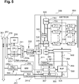
- the figure 5 illustrates an example of a system comprising a memory module adapted to implement calculation operations according to another embodiment.
- the system of figure 5 is similar to the system of picture 3 and differs from the system of the picture 3 essentially in that, in the system of figure 5 , the assembly comprising the control circuit 205 and the circuit 201 has been replaced by a module 500 (METEOR).
- METEOR module 500
- the module 500 is a reconfigurable module comprising a plurality of elementary blocks 510 arranged in a matrix according to K rows and P columns, with P an integer greater than or equal to 1, preferably greater than or equal to 2, for example greater than or equal to 3, and K integer greater than or equal to 1, preferably greater than or equal to 3.
- Each elementary block 510 comprises a memory circuit 511, also referenced "Tile i,j", with i integer ranging from 0 to K-1 (Tile 0.0; Tile 1.0; Tile K-1.0) and integer j ranging from 0 to P-1 (Tile 0.P-1; Tile 1.P-1; Tile K-1,P-1) designating respectively the position of the row and the position of the column of the elementary block in the matrix.
- Each memory circuit 511 is adapted to implement calculation functions. More particularly, each memory circuit 511 is adapted to load and store data, and to implement a certain number of logical and/or arithmetic operations having as operands the data stored in the memory circuit 511.
- Each memory circuit 511 is by example identical or similar to memory circuit 201 of the picture 3 .
- Each elementary block 510 further comprises a vertical transfer circuit 513, also referenced VTU, coupled to the memory circuit 511 of the block.
- the configurable transfer circuits 513 of any two adjacent elementary blocks 510 of the column are linked two by two by an uplink bus VTI-U and by a downlink bus VTI-D.
- the 500 memory module of the figure 5 further comprises an internal circuit 520 (TAM) for controlling the elementary blocks 510.
- the circuit 520 is in particular suitable for controlling the configuration of the vertical transfer circuits 513 of the elementary blocks 510 of the memory module.
- a TTC control bus internal to module 500 connects circuit 520 to control input ports (not detailed in the figure) of vertical transfer circuits 513 of the various elementary blocks 510 of the memory module.
- the circuit 520 is also suitable for controlling the reading and writing of data, as well as the implementation of calculation operations, in the memory circuits 511 of the elementary blocks 510 of the memory module.
- a TDI distribution bus internal to module 500 connects circuit 520 to data, address, and control input-output ports (not detailed in the figure) of memory circuits 511 of the various elementary blocks 510 of the memory module.
- the module 500 further comprises a circuit 530 (GPD) for global access regulation, as well as a circuit 540 (CSRs) for configuration registers.
- GPS global access regulation
- CSRs circuit 540
- Circuit 530 is connected to instruction distribution circuit 207 via link 209. Circuit 530 is adapted to schedule access to elementary blocks 510 of the memory circuit, to avoid address conflicts when executing instructions received from the memory circuit. processor 231 (via circuit 207). For this, the circuit 530 receives the instructions coming from the processor (via the circuit 207), and is adapted to insert one or more waiting cycles between different steps of the same instruction when a conflict potential is detected. Circuit 530 is particularly suitable for sending control data to circuit 520, via a control bus referenced Control on the figure 5 . Circuit 530 is also suitable for exchanging control data with arbitration circuit 309 of module 200. These exchanges are similar to the exchanges described previously between arbitration circuit 309 and control circuit 205 ( picture 3 ).
- the data exchanged between the arbitration circuit 309 and the control circuit 530 can also comprise configuration data of the matrix of elementary blocks 510.
- configuration data of the matrix of elementary blocks 510 in particular the size of the data vectors, can be indicated in the instructions sent by the processor 231 to the direct transfer circuit 203, for example during the writing of the instructions in the register 301.
- the logic circuit 305 can indicate to the arbitration circuit 309 a data size to be considered during a write or read operation in the memory circuit 500 requested by the logic circuit 305.
- Circuit 540 is adapted to store configuration data used by circuit 520 to configure vertical transfer circuits 513.
- Circuit 520 is adapted to read data from register circuit 540.
- Circuit 530 is adapted to read and write data in register circuit 540.
- An advantage of the 500 memory module of the figure 5 is that it is possible, via the control circuit 520 and the vertical transfer circuits 513, to virtually reconfigure the matrix of elementary blocks 510, either so as to extend the maximum dimension of the horizontal vectors that can be processed by the module memory, in particular for the implementation of calculation operations, either so as to increasing the number of vectors that can be processed (by reducing the maximum dimension of said horizontal vectors).
- the internal link 204 of the module 200 connects the buffer circuit 303 of the direct access circuit 203 to an input/output port (not detailed in the figure) of the reconfigurable module 500.
- a buffer circuit 560 interfaces between the link 204 and the input/output port of the module 500.
- the buffer 560 can, if necessary, make it possible to adapt the size of the data between the link 204 and the input/output port of the 500 module.
- the arbitration circuit 309 is adapted to exchange synchronization signals with the data transfer circuit 203, as previously described.
- buffer 560 contains a data vector ready to be written in module 500.
- Logic circuit 305 sends an elementary operation request, here a write, to the arbitration circuit.
- the arbitration circuit 309 authorizes, when possible, the writing of said ready data vector in the register 560 by sending a control signal, acknowledgment type, to the logic circuit 305.
- the logic circuit 305 controls the buffer circuit 303 in order to to read said data vector in the BUF circuit 303 and to write it in the register 560.
- the arbitration circuit 309 then sends an instruction signal to the control circuit 530 of the module 500, which controls the writing in the modulus 500 of the data vector present in register 560.
- a similar reverse process can be provided if it is desired to read a data vector in memory circuit 500 to transfer it to buffer circuit 303.
- the arbitration circuit exchanges request and acknowledgment signals with the logic circuit 305.
- Other operating variants can be envisaged, for example by using request or acknowledgment registers , for example present in the continuity of the registers 301.
- an advantage of the direct access circuit 203 is to allow direct transfers of data from or to the matrix of elementary modules 510 of the memory module 500, without blocking access to the processor.
- the presence of the internal link 204 makes it possible to avoid using a system bus to pass the data between the buffer circuit 303 and the memory circuit 500.
- This internal link 204 is thus a direct link between the transfer circuit direct 303 and the memory circuit, in the sense that it does not use the data exchange resources shared with the other elements of the circuit.
- This direct internal link is in a way a “private” link between the memory circuit and the direct transfer circuit.
- This direct internal connection 204 can in practice be achieved by simple wires connecting two registers, a register on the memory circuit side and a register on the data transfer circuit side 203, for example an input register of the buffer circuit 303.
- This direct connection can possibly include “buffer” type elements to amplify, or relay the signals transiting on the direct link.
- the direct link may optionally include logic gate type elements to enable possible synchronization or reinitialization functions of the direct link to be performed, in particular close to the inputs/outputs of the memory circuit 201, 500 or of the transfer circuit live 203.
Abstract
La présente description concerne un dispositif mémoire (200) comportant : un circuit mémoire (201) mettant en œuvre des opérations et réalisant des opérations élémentaires incluant une lecture, une écriture ou un calcul ; un circuit (205) de contrôle recevant des instructions d'un processeur (231), et décomposant chaque instruction reçue en plusieurs opérations élémentaires de façon à générer un flux de requête d'opérations élémentaires ; un circuit (203) de transfert direct de données depuis ou vers ledit circuit mémoire (201), le circuit de transfert (203) recevant des instructions du processeur (231), décomposant chaque instruction reçue en plusieurs opérations élémentaires à réaliser dans ledit circuit mémoire de façon à générer un flux de requête d'opérations élémentaires ; une liaison interne (204) d'échange de données reliant directement ledit circuit mémoire (201) au circuit de transfert direct (203) ; et un circuit d'arbitrage (309).The present description relates to a memory device (200) comprising: a memory circuit (201) implementing operations and performing elementary operations including reading, writing or calculation; a control circuit (205) receiving instructions from a processor (231), and breaking down each instruction received into several elementary operations so as to generate a request stream of elementary operations; a circuit (203) for direct transfer of data from or to said memory circuit (201), the transfer circuit (203) receiving instructions from the processor (231), breaking down each instruction received into several elementary operations to be carried out in said memory circuit so as to generate a request stream of elementary operations; an internal data exchange link (204) directly connecting said memory circuit (201) to the direct transfer circuit (203); and an arbitration circuit (309).
Description
La présente description concerne de façon générale le domaine des circuits mémoire, et vise plus particulièrement le domaine des circuits mémoire adaptés à mettre en oeuvre des opérations de calcul.The present description generally relates to the field of memory circuits, and is more particularly aimed at the field of memory circuits adapted to implement calculation operations.
On a déjà proposé des circuits mémoire adaptés à mettre en oeuvre des opérations de calcul, ou circuit mémoire « intelligents » (souvent appelé « smart memory » en anglais). De tels circuits sont par exemple destinés à coopérer avec un processeur, de façon à décharger le processeur de certaines tâches de calcul.Memory circuits adapted to implement calculation operations, or “intelligent” memory circuits (often called “smart memory”) have already been proposed. Such circuits are for example intended to cooperate with a processor, so as to relieve the processor of certain calculation tasks.
Néanmoins, les données utilisées pour les opérations de calcul demandées par un processeur à un tel circuit mémoire « intelligent » ne sont malheureusement pas toujours présentes dans la mémoire intelligente. En outre, même si elles sont présentes dans la mémoire, elles ne sont pas forcément mémorisées dans un espace souhaité de la mémoire, ou selon un ordre de stockage idéal, ce qui peut nécessiter des opérations de manipulation de données dans la mémoire par des lectures/écritures orchestrées par le processeur. Ainsi, il est souhaitable de trouver des solutions pour décharger encore davantage l'utilisation du processeur et de façon générale les canaux d'échange de données utilisés par le processeur.Nevertheless, the data used for the calculation operations requested by a processor from such an “intelligent” memory circuit are unfortunately not always present in the intelligent memory. Furthermore, even if they are present in memory, they are not necessarily stored in a desired space of memory, or in an ideal storage order, which may require data manipulation operations in memory by reads /processor-orchestrated writes. Thus, it is desirable to find solutions to further offload the use of the processor and in general the data exchange channels used by the processor.
Pour cela, un mode de réalisation prévoit un dispositif mémoire comportant :
- un port de connexion du dispositif à un processeur ;
- un circuit mémoire adapté à mettre en oeuvre des opérations de calcul et à réaliser des opérations élémentaires incluant une lecture, une écriture ou un calcul ;
- un premier circuit de contrôle adapté à recevoir des premières instructions en provenance du processeur via ledit port, et à décomposer chaque première instruction reçue en une séquence d'une ou de plusieurs opérations élémentaires de façon à générer un premier flux de requête d'opérations élémentaires ;
- un circuit de transfert direct de données depuis ou vers ledit circuit mémoire, le circuit de transfert direct étant adapté à recevoir des deuxièmes instructions en provenance du processeur via ledit port, à décomposer chaque deuxième instruction reçue en une séquence de plusieurs opérations élémentaires à réaliser dans ledit circuit mémoire de façon à générer un deuxième flux de requête d'opérations élémentaires ;
- une liaison interne d'échange de données reliant directement ledit circuit mémoire au circuit de transfert direct ; et
- un circuit d'arbitrage adapté à recevoir les premier et deuxième flux de requête d'opérations élémentaires et à commander le premier circuit de contrôle pour exécuter un unique flux global de requête d'opérations élémentaires dans le circuit mémoire mettant en oeuvre des règles de priorité prédéfinies dans le cas de requêtes simultanées d'accès au circuit mémoire,
- a connection port of the device to a processor;
- a memory circuit adapted to implement calculation operations and to carry out elementary operations including reading, writing or calculation;
- a first control circuit adapted to receive first instructions from the processor via said port, and to break down each first instruction received into a sequence of one or more elementary operations so as to generate a first request stream of elementary operations ;
- a direct data transfer circuit from or to said memory circuit, the direct transfer circuit being adapted to receive second instructions from the processor via said port, to break down each second instruction received into a sequence of several elementary operations to be carried out in said memory circuit so as to generate a second elementary operation request stream;
- an internal data exchange link directly connecting said memory circuit to the direct transfer circuit; and
- an arbitration circuit adapted to receive the first and second elementary operation request streams and to command the first control circuit to execute a single global elementary operation request stream in the memory circuit implementing priority rules predefined in the case of simultaneous requests for access to the memory circuit,
Selon un mode de réalisation, le circuit de transfert direct comprend un circuit buffer adapté à stocker temporairement des données transitant depuis ou vers le circuit mémoire.According to one embodiment, the direct transfer circuit comprises a buffer circuit adapted to temporarily store data transiting from or to the memory circuit.
Selon un mode de réalisation, le dispositif comprend un circuit de distribution connecté audit port de connexion du dispositif au processeur, le circuit de distribution recevant les premières et deuxièmes instructions en provenance du processeur et étant adapté à transmettre les premières instructions au premier circuit de contrôle et les deuxièmes instructions au circuit de transfert direct, le circuit de distribution utilisant une information d'adresse présente dans l'instruction pour réaliser cette distribution.According to one embodiment, the device comprises a distribution circuit connected to said connection port of the device to the processor, the distribution circuit receiving the first and second instructions from the processor and being adapted to transmit the first instructions to the first control circuit and the second instructions to the direct transfer circuit, the distribution circuit using address information present in the instruction to carry out this distribution.
Selon un mode de réalisation, la liaison interne a une largeur de données égale à la taille du plus grand vecteur de données pouvant être lu en une fois dans ledit circuit mémoire.According to one embodiment, the internal link has a data width equal to the size of the largest data vector that can be read at once in said memory circuit.
Selon un mode de réalisation, la liaison interne a une largeur de données au moins deux fois supérieure à la largeur de données du port de connexion du dispositif au processeur.According to one embodiment, the internal link has a data width at least twice greater than the data width of the connection port of the device to the processor.
Selon un mode de réalisation, le circuit de transfert direct est connecté à un port de connexion du module à un bus système mémoire externe au dispositif.According to one embodiment, the direct transfer circuit is connected to a connection port of the module to a memory system bus external to the device.
Selon un mode de réalisation, le port de connexion du dispositif au bus système mémoire présente une largeur de données supérieure à la largeur de données du port de connexion du dispositif au processeur.According to one embodiment, the connection port of the device to the memory system bus has a data width greater than the data width of the connection port of the device to the processor.
Selon un mode de réalisation, le circuit buffer du circuit de transfert direct est adapté à stocker temporairement des données transitant entre ledit circuit mémoire et un circuit mémoire externe relié audit bus système mémoire.According to one embodiment, the buffer circuit of the direct transfer circuit is suitable for temporarily storing data transiting between said memory circuit and an external memory circuit connected to said memory system bus.
Selon un mode de réalisation, le circuit de transfert direct comprend des registres de configuration stockant les deuxièmes instructions reçues en provenance du processeur.According to one embodiment, the direct transfer circuit comprises configuration registers storing the second instructions received from the processor.
Selon un mode de réalisation, le circuit de transfert direct comprend en outre un deuxième circuit de contrôle adapté à lire et écrire dans les registres de configuration, à échanger des données de contrôle avec le circuit d'arbitrage, et à commander des transferts de données via le circuit buffer.According to one embodiment, the direct transfer circuit further comprises a second control circuit adapted to read and write in the configuration registers, to exchange control data with the arbitration circuit, and to control data transfers via the buffer circuit.
Selon un mode de réalisation, ledit circuit mémoire comprend une pluralité de circuits mémoire adaptés à mettre en oeuvre des opérations de calcul, lesdits circuits mémoire étant agencés en matrice selon des rangées et des colonnes.According to one embodiment, said memory circuit comprises a plurality of memory circuits adapted to implement calculation operations, said memory circuits being arranged in a matrix according to rows and columns.
Selon un mode de réalisation, la matrice de circuits mémoire est reconfigurable de façon à ajuster la dimension des vecteurs de données dans la direction des rangées.According to one embodiment, the memory circuit array is reconfigurable so as to adjust the dimension of the data vectors in the direction of the rows.
Un mode de réalisation prévoit un système comportant un dispositif mémoire, un processeur adapté à transmettre les premières et deuxièmes instructions au dispositif mémoire, un bus système mémoire relié au circuit de transfert direct du dispositif mémoire, et un circuit mémoire externe relié au bus système mémoire, dans lequel le circuit de transfert direct est adapté à transférer des données directement entre le circuit mémoire du dispositif et le circuit mémoire externe via le bus système mémoire, sans passer par le processeur.One embodiment provides a system comprising a memory device, a processor adapted to transmit the first and second instructions to the memory device, a memory system bus connected to the direct transfer circuit of the memory device, and an external memory circuit connected to the memory system bus , in which the direct transfer circuit is adapted to transfer data directly between the memory circuit of the device and the external memory circuit via the memory system bus, without going through the processor.
Ces caractéristiques et avantages, ainsi que d'autres, seront exposés en détail dans la description suivante de modes de réalisation particuliers faite à titre non limitatif en relation avec les figures jointes parmi lesquelles :
- la
figure 1 représente de façon schématique un exemple d'un circuit mémoire adapté à mettre en oeuvre des opérations de calcul ; - la
figure 2 représente de façon schématique un exemple d'un système comportant un module mémoire adapté à mettre en oeuvre des opérations de calcul et un circuit de transfert de données couplé audit module mémoire selon un mode de réalisation ; - la
figure 3 illustre plus en détail un exemple d'implémentation du système de lafigure 2 ; - la
figure 4 représente un exemple de réalisation d'un circuit de transfert de données du module mémoire de lafigure 3 ; et - la
figure 5 illustre un autre exemple d'un système comportant un module mémoire adapté à mettre en oeuvre des opérations de calcul et un circuit de transfert de données couplé audit module mémoire selon un autre mode de réalisation.
- the
figure 1 schematically represents an example of a memory circuit adapted to implement calculation operations; - the
picture 2 schematically represents an example of a system comprising a memory module adapted to implement calculation operations and a data transfer circuit coupled to said memory module according to one embodiment; - the
picture 3 further illustrates an example system implementation of thepicture 2 ; - the
figure 4 represents an embodiment of a data transfer circuit of the memory module of thepicture 3 ; and - the
figure 5 illustrates another example of a system comprising a memory module adapted to implement calculation operations and a data transfer circuit coupled to said memory module according to another embodiment.
De mêmes éléments ont été désignés par de mêmes références dans les différentes figures. En particulier, les éléments structurels et/ou fonctionnels communs aux différents modes de réalisation peuvent présenter les mêmes références et peuvent disposer de propriétés structurelles, dimensionnelles et matérielles identiques.The same elements have been designated by the same references in the different figures. In particular, the structural and/or functional elements common to the various embodiments may have the same references and may have identical structural, dimensional and material properties.
Par souci de clarté, seuls les étapes et éléments utiles à la compréhension des modes de réalisation décrits ont été représentés et sont détaillés. En particulier, la réalisation des différents éléments des modules mémoire et des systèmes décrits n'a pas été détaillée, la réalisation de ces éléments étant à la portée de la personne du métier à partir des indications de la présente description. En particulier, la réalisation des circuits mémoire adaptés à mettre en oeuvre des opérations de calcul n'a pas été détaillée.For the sake of clarity, only the steps and elements useful for understanding the embodiments described have been represented and are detailed. In particular, the production of the various elements of the memory modules and of the systems described has not been detailed, the production of these elements being within the reach of a person skilled in the art based on the indications of the present description. In particular, the production of memory circuits suitable for implementing calculation operations has not been detailed.
Sauf précision contraire, lorsque l'on fait référence à deux éléments connectés entre eux, cela signifie directement connectés sans éléments intermédiaires autres que des conducteurs, et lorsque l'on fait référence à deux éléments reliés (en anglais "coupled") entre eux, cela signifie que ces deux éléments peuvent être connectés ou être reliés par l'intermédiaire d'un ou plusieurs autres éléments.Unless otherwise specified, when reference is made to two elements connected together, this means directly connected without intermediate elements other than conductors, and when reference is made to two elements connected (in English "coupled") between them, it means that these two elements can be connected or be linked via one or more other elements.
Sauf précision contraire, les expressions "environ", "approximativement", "sensiblement", et "de l'ordre de" signifient à 10 % près, de préférence à 5 % près.Unless specified otherwise, the expressions “about”, “approximately”, “substantially”, and “of the order of” mean to within 10%, preferably within 5%.
La
Le circuit mémoire 101 comprend en outre un circuit de sélection de rangées 107 (RS) adapté à sélectionner une unique rangée de la matrice 103 pour réaliser une opération de lecture ou d'écriture classique. Le circuit de sélection de rangées 107 peut en outre être adapté à sélectionner simultanément en lecture plusieurs rangées de la matrice 103, de façon à mettre en oeuvre, sur des pistes conductrices de sortie de colonne de la matrice, des opérations logiques de base ayant pour opérandes des données stockées dans les rangées sélectionnées.The memory circuit 101 further comprises a row selection circuit 107 (RS) adapted to select a single row of the
Le circuit mémoire 101 peut par ailleurs comprendre un circuit de calcul 109 (ALU) adapté à mettre en oeuvre des opérations de calcul supplémentaires à partir des signaux lus sur les pistes conductrices de sortie de colonne de la matrice 103 et/ou à réécrire directement dans la matrice 103 le résultat d'une opération de calcul, sans passer par des bornes de connexion externes du circuit mémoire 101.The memory circuit 101 can also comprise a calculation circuit 109 (ALU) adapted to implement additional calculation operations from the signals read on the conductive column output tracks of the
Le circuit mémoire 101 comprend en outre un circuit d'entrée/sortie 111 (I/O) reliant les colonnes de la matrice à des bornes de connexion à l'extérieur du circuit mémoire, par exemple à un port d'entrée/sortie de données (non détaillé sur la
Le circuit mémoire de la
La demande de brevet
La
Le module mémoire 200 de la
Le circuit mémoire 201 peut être un circuit mémoire de type IMC (de l'anglais "In Memory Computing" - calcul en mémoire), c'est-à-dire dans lequel des calculs sont mis en oeuvre directement au sein de la matrice de cellules élémentaires du circuit mémoire, par exemple tel que décrit en relation avec la
Le système de la
Selon un aspect d'un mode de réalisation, le module 200 comprend en outre un circuit 203 (DIMA) d'accès direct au circuit 201. Le circuit 203 est relié directement au circuit mémoire 201, par l'intermédiaire d'une liaison de transfert de données 204 interne au module 200. Le circuit 203 est en outre relié directement à un bus système de transfert de données 251 (MSB), aussi appelé bus système mémoire ("memory system bus" en anglais) externe au module 200, par l'intermédiaire d'une liaison 241. Dans cet exemple, le bus système mémoire 251 n'est pas directement connecté au processeur 231. Le bus 251 est un bus spécifiquement dédié au transfert direct (i.e. sans passer par le processeur 231) de données entre le circuit mémoire 201 du module 200 et d'autres circuits périphériques du système, par exemple une mémoire distante, ou toute autre mémoire interne ou externe susceptible d'échanger des données avec le circuit mémoire 201. Le bus 251 peut notamment comprendre un bus de données, un bus d'adresses et/ou un bus de contrôle. Le bus 251 peut être implémenté au moyen d'un système d'interconnexion distribué de type réseau sur puce ("network on chip" en anglais).According to one aspect of an embodiment, the
On notera que le bus mémoire système 251 et le bus système 239 peuvent avantageusement être reliés l'un à l'autre par différents circuits d'interface comme cela est connu de l'homme de l'art. En outre, le bus système 239 et le bus système mémoire 251 peuvent être un même et unique bus, même si cela n'est pas le mode de réalisation préférentiel. En effet, le bus système 239 est souvent de petite taille pour les données et mettre les deux bus en commun aurait sans doute pour conséquence d'avoir un bus 251 de petite taille, et de surcroît d'augmenter le débit nécessaire sur le bus commun ce qui pourrait en pratique se traduire par une saturation du bus, et par ricochet une diminution du débit d'échanges de données par rapport à une configuration à deux bus.It will be noted that the
De préférence, le bus système mémoire 251 est plus large que le bus système processeur 239. La liaison de transfert de données 204 a de préférence une largeur égale à la taille du plus grand vecteur de données pouvant être lu en une fois dans le circuit mémoire 201, par exemple égale à la taille d'une rangée de circuits de lecture présents en pieds de colonnes dans la matrice de cellules élémentaires de stockage du circuit mémoire 201. Dans le cas où il n'y a pas de multiplexage en pied de colonne, la taille de ce plus grand vecteur de données peut être égale à N bits si l'on considère l'exemple de la
Le circuit d'accès direct 203 est adapté à transférer des données directement, c'est-à-dire sans faire transiter ces données par le processeur 231, entre le circuit mémoire 201 et le bus système mémoire 251. Dans l'exemple représenté, le système comprend en outre un circuit mémoire 253 (MM) externe au module 200. Le circuit mémoire 253 est relié au bus système mémoire 251 par l'intermédiaire d'une liaison 255. Ainsi, le circuit d'accès direct 203 permet de transférer des données directement, c'est-à-dire sans faire transiter ces données par le processeur 231, entre le circuit mémoire 201 du module 200 et le circuit mémoire externe 253. Plus généralement, le circuit d'accès direct 203 permet de transférer des données directement, c'est-à-dire sans faire transiter ces données par le processeur 231, entre le circuit mémoire 201 du module 200 et tout circuit périphérique connecté au bus système mémoire 251. A titre d'exemples non limitatif, le circuit mémoire 253 peut être une mémoire de type SRAM, une mémoire de type NVM (de l'anglais "Non Volatil Memory" - mémoire non volatile), une mémoire de type DRAM (de l'anglais "Dynamic Random Access Memory" - mémoire dynamique à accès aléatoire), une mémoire de type Flash, ou encore un autre circuit mémoire adapté à mettre en oeuvre des opérations de calcul. Les différents composants du module 200 peuvent être intégrés dans une même puce de circuits intégrés. Le circuit mémoire 253 peut être intégré à cette même puce, ou externe à cette puce.The
Dans l'exemple de la
Les instructions envoyées par le processeur peuvent être des instructions simples correspondant à une unique requête d'écriture ou de lecture dans la mémoire sans opérations de calcul, ou peuvent être des instructions complexes pouvant nécessiter en pratique l'exécution de plusieurs opérations élémentaires de lecture, écriture ou calcul. Ainsi, le circuit 205 va procéder à une décomposition d'une instruction reçue en une séquence de plusieurs opérations élémentaires uniquement quand il reçoit une instruction complexe (ou « smart instruction » en anglais).The instructions sent by the processor may be simple instructions corresponding to a single write or read request in the memory without calculation operations, or may be complex instructions which may in practice require the execution of several elementary read operations, writing or calculation. Thus,
Les instructions complexes sont, après décodage, transformées en un flux d'opérations élémentaires, ou autrement dit une séquence d'opérations élémentaires. Par exemple, si une instruction complexe correspond à l'opération ET entre deux opérandes et à la mise en mémoire du résultat, la séquence élémentaire correspondant à cette instruction complexe va par exemple correspondre à :
- dans le cas d'une mémoire NMC : 1/ lire première opérande, 2/ lire deuxième opérande, 3/ calcul de l'opération ET, 4/ écriture résultat ;
- dans le cas d'une mémoire IMC : 1/
lire opérandes 1 et 2 par multi sélection de lignes et configuration du circuit de lecture pour réaliser une opération ET lors de la lecture, 2/ écriture du résultat.
- in the case of an NMC memory: 1/ read first operand, 2/ read second operand, 3/ calculation of the AND operation, 4/ write result;
- in the case of an IMC memory: 1/ read
operands 1 and 2 by multiple selection of lines and configuration of the read circuit to perform an AND operation during reading, 2/ writing of the result.
Dans le cas où la mémoire 201 peut, de par sa structure, réaliser plusieurs opérations élémentaires simultanément, il est alors possible de paralléliser certaines opérations élémentaires. Ainsi, il est possible de démarrer une séquence d'opérations correspondant à une n-ième instruction sans avoir terminé l'exécution d'une (n-1)-ième instruction. Autrement dit, des opérations élémentaires parallélisées peuvent correspondre à des instructions simples ou complexes différentes. Afin d'éviter des erreurs d'exécution de la séquence d'instructions reçues liées à cette possibilité de parallélisation, le circuit 205 peut dans ce cas inclure un dispositif d'analyse des séquences d'opérations correspondant aux instructions successives, pour insérer si besoin un ou des cycles d'attente dans une séquence d'opérations élémentaires correspondant à une instruction, lorsqu'un conflit potentiel est détecté.In the case where the
Le module 200 de la
Le processeur 231 peut requérir des accès en lecture ou en écriture au circuit mémoire 201, ou encore l'exécution de calculs par le circuit mémoire 201. Le processeur peut en outre requérir des transferts directs (via le circuit 203) de données entre le circuit mémoire 201 et un circuit périphérique externe au module 200, par exemple le circuit mémoire 253. Ces requêtes sont réparties entre le circuit de contrôle 205 et le circuit d'accès direct 203 par le circuit de distribution 207.The
Dans le système de la
La largeur relativement grande de la liaison interne 204 permet in fine de transférer, via le circuit de transfert direct 203, des volumes de données plus importants par rapport au cas où le bus de donnée 204 est de même taille, pour les données, que celle du port de connexion 233. En effet, pour un accès en mémoire demandé par le circuit de transfert direct 203, il est possible d'écrire/lire en parallèle plus de données en passant par la liaison interne 204 qu'en passant par le port de connexion 233 en provenance/à destination du CPU 231.The relatively large width of the
On notera que l'utilisation d'un circuit de transfert direct 203 associé à une mémoire 201 permettant de faire du calcul, notamment du calcul de type SIMD de l'anglais « Single Instruction Multiple Data », permet d'avoir en très grande majorité des écritures/lectures de données vers/depuis la mémoire qui passent par le circuit de transfert direct 203. Les échanges entre le CPU et la mémoire 201 sont alors majoritairement des transferts « d'instructions » visant à lancer des opérations de calcul (SIMD) et très peu des transferts classiques consistant à réaliser une simple lecture ou écriture de données en mémoire (sans lancer d'opérations de calcul).It will be noted that the use of a
La
Le système de la
Dans l'exemple de la
Plus particulièrement, dans cet exemple, le circuit 203 comprend un ensemble 301 (DMA CSRs) de registres d'état aussi appelés registres de configuration recevant les instructions en provenance du processeur 231, par l'intermédiaire de la liaison 211. Les registres 301 stockent les instructions de transfert à exécuter par le circuit 203. A titre d'exemple, les registres 301 stockent les plages d'adresses source et destination des transferts à réaliser. Les registres 301 peuvent en outre stocker la taille des blocs de données à transférer. Les instructions de transfert stockées dans les registres 301 peuvent en outre comprendre des instructions spécifiques au circuit d'accès direct 203 de réarrangement des données à l'intérieur du circuit d'accès direct 203, de manière à permettre de modifier l'arrangement des données lors de leur transfert entre la source et la destination.More particularly, in this example, the
Le circuit 203 comprend en outre un circuit buffer 303 (BUF) relié au circuit mémoire 201 par l'intermédiaire de la liaison interne 204, et au bus système mémoire 251 par l'intermédiaire d'une liaison de transfert de données 321. Le circuit buffer 303 stocke temporairement les données transitant du circuit mémoire 201 vers le bus système mémoire 251, ou du bus système mémoire 251 vers le circuit mémoire 201.
Le circuit 203 comprend de plus un circuit logique de contrôle 305 (CL). Le circuit logique de contrôle 305 est relié d'une part aux registres d'état 301 et d'autre part au circuit buffer 303. Le circuit 305 est adapté à commander des transferts de données éventuellement à l'intérieur du circuit buffer 303, mais surtout entre le circuit buffer 303 et les liaisons 204 et 321, en fonction de l'état de l'exécution d'une instruction préalablement stockée dans les registres 301. Lorsque l'exécution d'une instruction de transfert de données requise par le processeur 231 est terminée, le circuit logique de contrôle 305 renvoie une interruption au processeur 231 pour l'en informer. L'interruption peut être transmise par une liaison 323 (DMA interrupt) connectant le circuit 305 au processeur 231.
Le circuit 203 comprend en outre un circuit de génération d'adresses 307 (AG). Le circuit 307 est relié au circuit logique de contrôle 305. Le circuit 307 est en outre relié au bus système mémoire 251 par l'intermédiaire d'une liaison de transfert de signaux d'adresse 325. Le circuit de génération d'adresses 307 est adapté à générer une séquence de signaux d'adresse pour transférer successivement les données entre le circuit buffer 303 et le bus 251, conformément aux instructions stockées dans les registres 301.
Dans l'exemple représenté en
Dans l'exemple de la
Par ailleurs, dans l'exemple de la
Dans l'exemple de la
- un premier flux correspondant aux instructions envoyées par le processeur 231
au circuit mémoire 201, généré par le circuit de contrôle 205 ; et - un deuxième flux correspondant à l'exécution des transferts de données entre le circuit mémoire 201 et la mémoire externe 253, généré par le circuit de contrôle 305.
- a first stream corresponding to the instructions sent by the
processor 231 to thememory circuit 201, generated by thecontrol circuit 205; and - a second flow corresponding to the execution of the data transfers between the
memory circuit 201 and theexternal memory 253, generated by thecontrol circuit 305.
Les requêtes reçues par le circuit d'arbitrage 309 en provenance du circuit de contrôle 205 et du circuit de contrôle 305 sont autorisées ou retardées par le circuit d'arbitrage en fonction des conflits potentiels de demandes d'accès au circuit mémoire 201. Autrement dit, le circuit d'arbitrage 309 transmet au circuit de contrôle 205 du circuit mémoire 201 un unique flux de requête d'opérations élémentaires, appelé flux global, correspondant à une combinaison entrelacée des premier et deuxième flux, selon un ordonnancement défini par des règles de priorité prédéfinies. La granularité de l'entrelacement des premier et deuxième flux peut être à l'échelle des opérations élémentaires, ou à une échelle plus haut niveau, c'est-à-dire à une échelle de groupes d'opérations élémentaires.The requests received by the
Les instructions envoyées par le processeur 231 au circuit de contrôle 205 ou écrites dans les registres de configuration 301 peuvent comporter des bits de priorité exploités in fine par le circuit d'arbitrage 309 pour décider de l'ordre de traitement des opérations élémentaires. Ainsi, selon un mode de réalisation, les premier et deuxième flux de requête d'opérations élémentaires reçus par le circuit d'arbitrage 309 peuvent chacun inclure un ou des bits de priorité indiquant la priorité correspondante de chaque opération élémentaire en fonction de la priorité indiquée par le processeur lors de l'envoi de l'instruction correspondante. Dans le cas par exemple où le circuit d'arbitrage 309 reçoit simultanément des requêtes d'opérations élémentaires pour chacun des premier et deuxième flux, alors une règle par défaut peut être donnée pour leur traitement. On peut par exemple donner toujours priorité au premier flux, ou donner priorité à tour de rôle entre les deux flux.The instructions sent by the
La liaison 204 reliant le circuit mémoire 201 au circuit d'accès direct 203, permettant de réaliser des transferts directs (sans passer par le processeur 231) de données entre le circuit mémoire 201 et la mémoire distante 253 est par exemple adaptée à transmettre uniquement des signaux de données correspondant aux données lues ou à écrire dans le circuit mémoire 201 et correspondant respectivement à des données écrites ou lues dans le circuit buffer 303.The
La largeur des données pouvant être transmises simultanément via la liaison 204 est par exemple égale ou supérieure à la largeur du bus système mémoire 251. Les modes de réalisation décrits ne se limitent toutefois pas à ce cas particulier.The width of the data that can be transmitted simultaneously via the
Pour chaque requête d'opération élémentaire du deuxième flux, des signaux d'adresse et de contrôle utilisés pour indiquer l'adresse de chaque donnée à transférer, le type d'accès à réaliser (lecture ou écriture), la taille de la donnée à transférer, etc., peuvent être transmis par le circuit 305 au circuit de contrôle 205 du circuit mémoire 201, via le circuit d'arbitrage ou éventuellement directement. Quel que soit le mode de réalisation, il est nécessaire de prévoir un mécanisme de synchronisation entre le circuit d'arbitrage, le circuit de contrôle 205 et le circuit de transfert direct afin d'assurer que les signaux d'adresse et de contrôle correspondant à une requête d'opération élémentaire émise par le circuit logique 305 soient pris en compte par le circuit mémoire pour l'exécution de l'opération élémentaire en même temps que les données à écrire ou lire dans le circuit buffer 303 transitent sur la liaison 204 pour cette même opération élémentaire. Ainsi, par exemple, on peut prévoir qu'une requête d'opération élémentaire transmise au circuit d'arbitrage par le circuit logique 305 inclut toutes les informations d'adresse et de contrôle et que le circuit d'arbitrage envoie au circuit logique 305 une information, type requête d'acquittement, pour lui signifier qu'il lance l'exécution de l'opération élémentaire dans le circuit mémoire 201, et par suite que le circuit de transfert de données peut envoyer une donnée sur la liaison 204 (dans le cas d'une écriture dans le circuit mémoire 201) ou récupérer une donnée sur la liaison 204 (dans le cas d'une lecture dans le circuit mémoire 201). D'autres mécanismes de synchronisation entre le circuit d'arbitrage 309, le circuit mémoire 201 et le circuit de transfert direct 203 peuvent bien entendu être mis en place.For each elementary operation request of the second stream, address and control signals used to indicate the address of each data to be transferred, the type of access to be performed (read or write), the size of the data to transfer, etc., can be transmitted by the
En outre, le circuit d'arbitrage a été représenté précédemment comme un circuit différent du circuit de contrôle 205 du circuit mémoire 201 afin principalement de mettre en avant la fonction, le rôle, d'arbitrage indispensable à la mise en œuvre d'un circuit selon la présente invention dans lequel deux flux de requête d'opérations élémentaires souhaitent accéder à une même ressource, à savoir la matrice 103 et les moyens de calcul en mémoire (par exemple 107). Cette fonction d'arbitrage pourrait par exemple être réalisée par le circuit de contrôle 205 du circuit mémoire 201. Le circuit de contrôle 205 dialoguerait ainsi directement avec le circuit logique 305 et plus généralement le circuit de transfert direct 203 ; le circuit de contrôle 205 recevrait ainsi, via deux ports d'entrée/sortie, des requêtes d'instructions du processeur 231 et des requêtes d'instructions du circuit 203 sous forme de requêtes d'opérations élémentaires, ou sous forme éventuellement d'instructions plus haut niveau à décoder par le circuit 205 en utilisant par exemple le même décodeur que celui utilisé pour décoder les instructions provenant du processeur 231. Selon un autre mode de réalisation, le circuit décodeur d'instructions présent dans le circuit de contrôle 205 est « déporté » dans le circuit d'arbitrage 309 et le circuit de contrôle 205 traite et reçoit un unique flux global de requête d'opérations envoyé par le circuit d'arbitrage 309.In addition, the arbitration circuit has been represented previously as a circuit different from the
La
Plus particulièrement, sur la
Dans cet exemple, le circuit buffer 303 comprend deux sous-circuits de transfert unidirectionnel 401 et 403 de type FIFO (de l'anglais "First In First Out" - premier entré premier sorti). Le circuit 401 est adapté à transmettre des données du circuit mémoire 201 du module 200 vers le bus système mémoire 251. Le circuit 403 est quant à lui adapté à transmettre des données du bus système mémoire 251 vers le circuit mémoire 201. Le circuit 401 comprend un port d'entrée relié à un port de sortie du circuit mémoire 201 (non visible sur la
Les circuits 401 et 403 permettent de stocker temporairement les données pendant leur transfert du circuit mémoire 201 vers le bus système mémoire 251 ou du bus système mémoire 251 vers le circuit mémoire 201. Plus généralement, tout autre agencement du circuit buffer 303 adapté à remplir cette fonction peut être prévu.
Le circuit buffer 303 peut en outre avoir une fonction d'adaptation de la taille des données entre la liaison 204 et la liaison 321. A titre d'exemple, la liaison 204 peut avoir une largeur de données J, la liaison 321 peut avoir une largeur de données L, et le bus système mémoire 251 peut avoir une largeur de données I, avec J, L et I entiers supérieurs à 1. La largeur J peut être égale à la largeur L. A titre de variante, la largeur J peut être différente de la largeur L. Dans ce cas, le circuit buffer 303 est configuré pour adapter la taille des données transmises. Par exemple, la largeur J peut être supérieure à la largeur L. L'adaptation de la taille des données peut être réalisée par les registres 405, 407, 409 et 411. A titre d'exemple, les registres 409 et 411 peuvent être des registres à décalage. Par ailleurs, la largeur I peut être égale à la largeur L, ou différente de la largeur L. A titre d'exemple, la largeur I est inférieure à la largeur L. L'adaptation de taille des données (sérialisation) entre la liaison 321 et le bus système mémoire 251 peut être réalisée par le circuit d'interface 241a.The
A titre d'exemple, non limitatif, la largeur J est égale à 2048 bits, la largeur L est égale à 512 bits, et la largeur I est égale à 128 bits.By way of non-limiting example, the width J is equal to 2048 bits, the width L is equal to 512 bits, and the width I is equal to 128 bits.
La largeur des mots des buffers 401 et 403 est par exemple égale à la largeur J, ou à la largeur L.The width of the words of the
A titre d'exemple, lors d'une transmission de données du bus système mémoire 251 vers le circuit mémoire 201, le buffer 403 est rempli successivement par sous-mots de largeur L jusqu'à ce qu'un mot complet de largeur J soit disponible pour être transmis au circuit mémoire 201 via la liaison 204. Lors d'une transmission de données du circuit mémoire 201 vers le bus système mémoire 251, le buffer 401 est lu par sous-mots de largeur L, transmis successivement au bus système mémoire 251 via la liaison 321.By way of example, during a transmission of data from the
Du point de vue de la programmation, le circuit d'accès direct 203 du module 200 est contrôlé par le processeur 231 par l'intermédiaire des registres d'état 301. Des instructions dédiées sont utilisées pour contrôler les transferts de données via le circuit 203.From a programming perspective,
Les accès en écriture au circuit mémoire 201 du module 200, par exemple pour transférer des données depuis la mémoire externe 253 vers le circuit mémoire 201, via le circuit d'interface 241a et le circuit d'accès direct 203, peuvent être mis en oeuvre comme suit. D'abord, le processeur 231 écrit une instruction complète de transfert dans les registres de configuration 301 du circuit 203 via le circuit d'interface 233b et le circuit 207 de distribution des instructions du module 200. L'instruction comprend notamment l'adresse source des données à transférer (c'est-à-dire l'adresse des données dans la mémoire externe 253), la taille du bloc de données à transférer, l'adresse destination des données à transférer (c'est-à-dire l'adresse des données dans le circuit mémoire 201), et éventuellement une consigne de réagencement des données lors du transfert. Le circuit logique de contrôle 305 du circuit 203 génère ensuite une requête d'accès en lecture à la mémoire 253 à l'adresse source spécifiée (fournie par le générateur d'adresses 307). Cette requête est envoyée par le circuit d'interface 241a du module 200 au circuit d'interface 255a du circuit mémoire externe 253, via le bus système mémoire 251. Lorsque les données source sont prêtes, la mémoire externe 253 envoie l'ensemble des données requises, par exemple en salve continue, directement dans le circuit buffer 303 du circuit 203, via les circuits d'interface 255a et 241a et le bus système mémoire 251. Les données sont ensuite transférées du circuit buffer 303 vers le circuit mémoire 201, par l'intermédiaire de la liaison interne 204 du module 200, lorsque le circuit d'arbitrage 309 autorise ce transfert. Ce transfert peut être un transfert continu au fur et à mesure que les données sont rendues disponibles en sortie du circuit buffer 303. A titre de variante, on peut attendre que la totalité des données soit disponible dans le circuit buffer 303 pour réaliser le transfert vers le circuit mémoire 201. Le choix du mode de transfert peut être effectué en fonction d'une éventuelle différence de fréquence de fonctionnement entre la mémoire externe 253 et le circuit mémoire 201 du module 200. Lors du transfert, les adresses destination sont communiquées au circuit de contrôle 205 du circuit mémoire 201 par le circuit d'arbitrage 309. Lorsque l'exécution de l'instruction de transfert est terminée, une interruption est renvoyée par le circuit de contrôle 305 à destination du processeur.Write accesses to
Les accès en lecture au circuit mémoire 201 du module 200, par exemple pour transférer des données depuis le circuit mémoire 201 vers la mémoire externe 253, via le circuit d'accès direct 203 du module 200 et le circuit d'interface 241a, peuvent être réalisés selon un chemin inverse à ce qui vient d'être décrit. Le processeur 231 écrit d'abord l'instruction complète dans les registres de configuration 301 du circuit 203, via le circuit d'interface 233b et le circuit 207 de distribution des instructions du module 200. Le circuit logique de contrôle 305 du circuit 203 génère ensuite une requête d'accès en lecture au circuit mémoire 201 à l'adresse source spécifiée. Cette requête est transmise au circuit mémoire 201 par l'intermédiaire du circuit d'arbitrage 309 et du circuit de contrôle 205. Les données sont alors transférées du circuit mémoire 201 vers le circuit buffer 303 via la liaison 204. Le contenu du circuit buffer 303 est ensuite transféré à l'adresse destination de la mémoire externe 253, via la liaison 321, le circuit d'interface 241a, le bus système mémoire 251, et le circuit d'interface 255a.Read accesses to
Dans le système de la
On a décrit ci-dessus des exemples d'implémentation dans lesquels le module 200 comprend un unique circuit mémoire 201 adapté à mettre en oeuvre des opérations de calcul.Implementation examples have been described above in which the
A titre de variante, l'ensemble comprenant le circuit de contrôle 205 et le circuit 201 peut être remplacé par un module comprenant une pluralité de blocs élémentaires comprenant chacun un circuit mémoire adapté à mettre en oeuvre des opérations de calcul, par exemple du type décrit dans la demande de brevet
La
Le système de la
Le module 500 est un module reconfigurable comprenant une pluralité de blocs élémentaires 510 agencés en matrice selon K rangées et P colonnes, avec P entier supérieur ou égal à 1, de préférence supérieur ou égal à 2, par exemple supérieur ou égal à 3, et K entier supérieur ou égal à 1, de préférence supérieur ou égal à 3.The
Chaque bloc élémentaire 510 comprend un circuit mémoire 511, également référencé "Tile i,j", avec i entier allant de 0 à K-1 (Tile 0,0 ; Tile 1,0 ; Tile K-1,0) et j entier allant de 0 à P-1 (Tile 0,P-1 ; Tile 1,P-1 ; Tile K-1,P-1) désignant respectivement la position de la rangée et la position de la colonne du bloc élémentaire dans la matrice. Chaque circuit mémoire 511 est adapté à mettre en oeuvre des fonctions de calcul. Plus particulièrement, chaque circuit mémoire 511 est adapté à charger et stocker des données, et à mettre en oeuvre un certain nombre d'opérations logiques et/ou arithmétiques ayant pour opérandes les données stockées dans le circuit mémoire 511. Chaque circuit mémoire 511 est par exemple identique ou similaire au circuit mémoire 201 de la
Dans chaque colonne de la matrice, les circuits de transfert configurables 513 de deux blocs élémentaires 510 adjacents quelconques de la colonne sont reliés deux à deux par un bus de liaison montant VTI-U et par un bus de liaison descendant VTI-D. Autrement dit, dans chaque colonne de la matrice, dans chaque bloc élémentaire 510 de rang i de la colonne à l'exception des blocs élémentaires des première (i=0) et dernière (i=K-1) rangées de la matrice, le circuit de transfert vertical 513 du bloc est relié, par exemple connecté, au circuit de transfert vertical 513 du bloc élémentaire 510 de rang i-1 par un bus de liaison montant VTI-U et par un bus de liaison descendant VTI-D, et est relié, par exemple connecté, au circuit de transfert vertical 513 du bloc élémentaire 510 de rang i+1 par un autre bus de liaison montant VTI-U et par un autre bus de liaison descendant VTI-D.In each column of the matrix, the
Dans chaque colonne, le circuit de transfert vertical 513 du bloc élémentaire 510 de rang i=0 est relié, par exemple connecté, au circuit de transfert vertical 513 du bloc élémentaire 510 de rang i=1 par un bus de liaison montant VTI-U et par un bus de liaison descendant VTI-D. De plus, dans chaque colonne, le circuit de transfert vertical 513 du bloc élémentaire 510 de rang i=K-1 est relié, par exemple connecté, au circuit de transfert vertical 513 du bloc élémentaire 510 de rang i=K-2 par un bus de liaison montant VTI-U et par un bus de liaison descendant VTI-D.In each column, the
Dans cet exemple, dans chaque colonne de la matrice, dans chaque bloc élémentaire 510 de rang i de la colonne, à l'exception des blocs élémentaires 510 des première (i=0) et dernière (i=K-1) rangées de la matrice, le circuit de transfert vertical 513 du bloc est configurable pour :
- a) transmettre sur un bus d'écriture de données (non détaillés sur la
figure 1 ) du circuit mémoire 511 du bloc l'un ou l'autre de :- un mot de données reçu sur le bus de liaison descendant VTI-D reliant le circuit de transfert vertical 513 du bloc élémentaire 510 au circuit de transfert vertical 513 du bloc élémentaire 510 adjacent de rang i-1 dans la colonne ; et
- un mot de données reçu sur le bus de liaison montant VTI-U reliant le circuit de transfert vertical 513 du bloc élémentaire 510 au circuit de transfert vertical 513 du bloc élémentaire 510 adjacent de rang i+1 dans la colonne ;
- b) transmettre sur le bus de liaison montant VTI-U reliant le circuit de transfert vertical 513 du bloc élémentaire 510 au circuit de transfert vertical 513 du bloc élémentaire 510 adjacent de rang i-1 dans la colonne l'un ou l'autre de :
- un mot de données reçu sur un bus de lecture de données (non détaillé sur la
figure 1 ) du circuit mémoire 511 du bloc élémentaire ; et - un mot de données reçu sur le bus de liaison montant VTI-U reliant le circuit de transfert vertical 513 du bloc élémentaire 510 au circuit de transfert vertical 513 du bloc élémentaire 510 adjacent de rang i+1 dans la colonne ; et
- un mot de données reçu sur un bus de lecture de données (non détaillé sur la
- c) transmettre sur le bus de liaison descendant VTI-D reliant le circuit de transfert vertical 513 du bloc élémentaire 510 au circuit de transfert vertical 513 du bloc élémentaire adjacent de rang i + 1 dans la colonne l'un ou l'autre de :
- un mot de données reçu sur le bus de lecture de données du circuit mémoire 511 du bloc élémentaire ; et
- un mot de données reçu sur le bus de liaison descendant VTI-D reliant le circuit de transfert vertical 513 du bloc élémentaire 510 au circuit de transfert vertical 513 du bloc élémentaire 510 adjacent de rang i-1 dans la colonne.
- a) transmit on a data write bus (not detailed on the
figure 1 ) of thememory circuit 511 of the block either of:- a data word received on the VTI-D downlink bus connecting the
vertical transfer circuit 513 of the elementary block 510 to thevertical transfer circuit 513 of the adjacent elementary block 510 of rank i-1 in the column; and - a data word received on the uplink bus VTI-U connecting the
vertical transfer circuit 513 of the elementary block 510 to thevertical transfer circuit 513 of the adjacent elementary block 510 of rank i+1 in the column;
- a data word received on the VTI-D downlink bus connecting the
- b) transmitting on the uplink bus VTI-U connecting the
vertical transfer circuit 513 of the elementary block 510 to thevertical transfer circuit 513 of the adjacent elementary block 510 of rank i-1 in the one or other column of :- a data word received on a read data bus (not detailed on the
figure 1 ) of thememory circuit 511 of the elementary block; and - a data word received on the uplink bus VTI-U connecting the
vertical transfer circuit 513 of the elementary block 510 to thevertical transfer circuit 513 of the adjacent elementary block 510 of rank i+1 in the column; and
- a data word received on a read data bus (not detailed on the
- c) transmitting on the VTI-D downlink bus connecting the
vertical transfer circuit 513 of the elementary block 510 to thevertical transfer circuit 513 of the adjacent elementary block of rank i + 1 in the column either of:- a data word received on the data read bus of
memory circuit 511 of the elementary block; and - a data word received on the VTI-D downlink bus connecting the
vertical transfer circuit 513 of the elementary block 510 to thevertical transfer circuit 513 of the adjacent elementary block 510 of rank i-1 in the column.
- a data word received on the data read bus of
Dans chaque colonne, le circuit de transfert vertical 513 du bloc élémentaire 510 de rang i=0 est par exemple adapté à :
- transmettre un mot de données reçu sur le bus de lecture de données du circuit mémoire 511 du bloc 510 vers le bus de liaison descendant VTI-D reliant le bloc 510 au circuit de transfert vertical 513 du bloc élémentaire 510 adjacent de rang i=1 ; et/ou
- transmettre sur le bus d'écriture de données du circuit mémoire 511 du bloc 510 un mot de données reçu sur le bus de liaison montant VTI-U reliant le bloc 510 au circuit de transfert vertical 513 du bloc élémentaire 510 adjacent de rang i=1.
- transmitting a data word received on the data read bus from
memory circuit 511 of block 510 to the VTI-D downlink bus connecting block 510 tovertical transfer circuit 513 of adjacent elementary block 510 of rank i=1; and or - transmit on the data write bus of
memory circuit 511 of block 510 a word of data received on the uplink bus VTI-U connecting block 510 tovertical transfer circuit 513 of adjacent elementary block 510 of rank i=1 .
Dans chaque colonne, le circuit de transfert vertical 513 du bloc élémentaire 510 de rang i=K-1 est par exemple adapté à :
- transmettre un mot de données reçu sur le bus de lecture de données du circuit mémoire 511 du bloc 510 vers le bus de liaison montant VTI-U reliant le bloc 510 au circuit de transfert vertical 513 du bloc élémentaire 510 adjacent de rang i=K-2 ; et/ou
- transmettre sur le bus d'écriture de données du circuit mémoire 511 du bloc 510 un mot de données reçu sur le bus de liaison descendant VTI-D reliant le bloc 510 au circuit de transfert vertical 513 du bloc élémentaire 110 adjacent de rang i=K-2.
- transmit a data word received on the data read bus from
memory circuit 511 of block 510 to the uplink bus VTI-U connecting block 510 tovertical transfer circuit 513 of adjacent elementary block 510 of rank i=K- 2; and or - transmit on the circuit's data write
bus memory 511 of block 510 a word of data received on the VTI-D downlink bus connecting block 510 to thevertical transfer circuit 513 of the adjacent elementary block 110 of rank i=K-2.
Le module mémoire 500 de la
Le circuit 520 est en outre adapté à contrôler la lecture et l'écriture de données, ainsi que la mise en oeuvre d'opérations de calcul, dans les circuits mémoire 511 des blocs élémentaires 510 du module mémoire. Pour cela, un bus de distribution TDI interne au module 500 relie le circuit 520 à des ports d'entrée-sortie de données, d'adresse, et de contrôle (non détaillés sur la figure) des circuits mémoire 511 des différents blocs élémentaires 510 du module mémoire.The
Le module 500 comprend en outre un circuit 530 (GPD) de régulation globale des accès, ainsi qu'un circuit 540 (CSRs) de registres de configuration.The
Le circuit 530 est relié au circuit 207 de distribution des instructions via la liaison 209. Le circuit 530 est adapté à ordonnancer les accès aux blocs élémentaires 510 du circuit mémoire, pour éviter des conflits d'adresses lors de l'exécution des instructions reçues du processeur 231 (via le circuit 207). Pour cela, le circuit 530 reçoit les instructions provenant du processeur (via le circuit 207), et est adapté à insérer un ou plusieurs cycles d'attente entre différentes étapes d'une même instruction lorsqu'un conflit potentiel est détecté. Le circuit 530 est notamment adapté à envoyer des données de contrôle au circuit 520, via un bus de contrôle référencé Control sur la
Le circuit 540 est adapté à stocker des données de configuration utilisées par le circuit 520 pour configurer les circuits de transfert vertical 513. Le circuit 520 est adapté à lire des données dans le circuit de registres 540. Le circuit 530 est adapté à lire et écrire des données dans le circuit de registres 540.
Un avantage du module mémoire 500 de la
Dans cet exemple, la liaison interne 204 du module 200 relie le circuit buffer 303 du circuit d'accès direct 203 à un port d'entrée/sortie (non détaillé sur la figure) du module reconfigurable 500.In this example, the
Dans l'exemple représenté, un circuit buffer 560 fait interface entre la liaison 204 et le port d'entrée/sortie du module 500. Le buffer 560 peut, le cas échéant, permettre d'adapter la taille des données entre la liaison 204 et le port d'entrée/sortie du module 500.In the example represented, a
Dans cet exemple, le circuit d'arbitrage 309 est adapté à échanger des signaux de synchronisation avec le circuit de transfert de données 203, comme précédemment décrit. A titre d'exemple, le buffer 560 contient un vecteur de données prêt à être écrit dans le module 500. Le circuit logique 305 envoie une requête d'opération élémentaire, ici une écriture, au circuit d'arbitrage. Le circuit d'arbitrage 309 autorise, quand cela est possible, l'écriture dudit vecteur de données prêt dans le registre 560 en envoyant un signal de contrôle, type acquittement, au circuit logique 305. Le circuit logique 305 commande le circuit buffer 303 afin de lire ledit vecteur de données dans le circuit BUF 303 et de l'écrire dans le registre 560. Le circuit d'arbitrage 309 envoie ensuite un signal d'instruction au circuit de contrôle 530 du module 500, qui commande l'écriture dans le module 500 du vecteur de données présent dans le registre 560. Un processus similaire inverse peut être prévu dans le cas où l'on souhaite lire un vecteur de données dans le circuit mémoire 500 pour le transférer dans le circuit buffer 303.In this example, the
On notera que divers modes de commande du circuit buffer peuvent être envisagés, notamment pour la réalisation d'opérations de réarrangement. On pourra par exemple s'inspirer des exemples donnés dans les brevets
En outre, dans les exemples susmentionnés, le circuit d'arbitrage échange des signaux de requêtes et d'acquittement avec le circuit logique 305. D'autres variantes de fonctionnement peuvent être envisagées, en utilisant par exemple des registres de requête ou d'acquittement, par exemple présents dans la continuité des registres 301. De plus, il peut être envisagé des mécanismes d'échange direct de signaux entre le circuit d'arbitrage 309 et le circuit buffer 303, notamment pour synchroniser le transfert de données à travers la liaison 204, et l'écriture des données dans les registres destinataires côté circuit buffer, ou côté circuit mémoire 500, notamment le registre 560.Furthermore, in the aforementioned examples, the arbitration circuit exchanges request and acknowledgment signals with the
Là encore, un avantage du circuit d'accès direct 203 est de permettre des transferts directs de données depuis ou vers la matrice de modules élémentaires 510 du module mémoire 500, sans bloquer l'accès au processeur. En outre, la présence de la liaison interne 204 permet d'éviter d'utiliser un bus système pour faire transiter les données entre le circuit buffer 303 et le circuit mémoire 500. Cette liaison interne 204 est ainsi une liaison directe entre le circuit de transfert direct 303 et le circuit mémoire, dans le sens où elle n'utilise pas les ressources d'échange de données partagées avec les autres éléments du circuit. Cette liaison interne directe est en quelque sorte une liaison « privée » entre le circuit mémoire et le circuit de transfert direct. Cette liaison interne 204 directe, peut en pratique être réalisée par de simples fils reliant deux registres, un registre côté circuit mémoire et un registre côté circuit transfert de données 203, par exemple un registre d'entrée du circuit buffer 303. Cette liaison directe peut éventuellement comprendre des éléments de type « buffer » pour amplifier, ou relayer les signaux transitant sur la liaison directe. En outre, la liaison directe peut éventuellement inclure des éléments type porte logique pour permettre de réaliser d'éventuelles fonctions de synchronisation ou de réinitialisation de la liaison directe, notamment à proximité des entrées/sorties du circuit mémoire 201, 500 ou du circuit de transfert direct 203.Here again, an advantage of the
Par ailleurs, dans les exemples précédents, nous avons décrit des transferts de données entre le circuit mémoire 201 et un circuit mémoire externe 253. Selon une variante de réalisation, il est possible de prévoir des instructions émises par le processeur pour le circuit de transfert direct 203 visant à réaliser un transfert de données entre deux emplacements du circuit mémoire 201, 500. Dans ce cas, les données lues dans le circuit mémoire 201 transitent temporairement dans le circuit buffer 303 avant d'être écrites à nouveau dans le circuit mémoire dans un autre emplacement. Un tel transfert peut permettre en outre au passage de réagencer les données dans un ordre, une organisation spatiale différente, afin par exemple de faciliter la mise en oeuvre subséquente d'une opération de calcul sur ces données.Furthermore, in the preceding examples, we have described data transfers between the
Divers modes de réalisation et variantes ont été décrits. La personne du métier comprendra que certaines caractéristiques de ces divers modes de réalisation et variantes pourraient être combinées, et d'autres variantes apparaîtront à la personne du métier. En particulier, les modes de réalisation décrits ne se limitent pas aux exemples de valeurs numériques mentionnés dans la présente description.Various embodiments and variants have been described. Those skilled in the art will understand that certain features of these various embodiments and variations could be combined, and other variations will occur to those skilled in the art. In particular, the embodiments described are not limited to the examples of numerical values mentioned in the present description.
Enfin, la mise en oeuvre pratique des modes de réalisation et variantes décrits est à la portée de la personne du métier à partir des indications fonctionnelles données ci-dessus. En particulier, la réalisation des différents éléments fonctionnels des systèmes décrits sont à la portée de la personne du métier à partir des indications de la présente description.Finally, the practical implementation of the embodiments and variants described is within the abilities of those skilled in the art based on the functional indications given above. In particular, the realization of the different functional elements of the systems described are to be the scope of the person skilled in the art from the indications of this description.
Claims (13)
Applications Claiming Priority (1)
| Application Number | Priority Date | Filing Date | Title |
|---|---|---|---|
| FR2014174A FR3118528B1 (en) | 2020-12-28 | 2020-12-28 | Memory module suitable for implementing calculation functions |
Publications (1)
| Publication Number | Publication Date |
|---|---|
| EP4020475A1 true EP4020475A1 (en) | 2022-06-29 |
Family
ID=75438947
Family Applications (1)
| Application Number | Title | Priority Date | Filing Date |
|---|---|---|---|
| EP21216400.8A Pending EP4020475A1 (en) | 2020-12-28 | 2021-12-21 | Memory module suitable for performing computing functions |
Country Status (3)
| Country | Link |
|---|---|
| US (1) | US11482264B2 (en) |
| EP (1) | EP4020475A1 (en) |
| FR (1) | FR3118528B1 (en) |
Cited By (1)
| Publication number | Priority date | Publication date | Assignee | Title |
|---|---|---|---|---|
| CN115981751A (en) * | 2023-03-10 | 2023-04-18 | 之江实验室 | Near memory computing system, near memory computing method, device, medium and equipment |
Families Citing this family (1)
| Publication number | Priority date | Publication date | Assignee | Title |
|---|---|---|---|---|
| CN117714388A (en) * | 2024-02-04 | 2024-03-15 | 极芯通讯技术(安吉)有限公司 | Hybrid circuit transmission and packet transmission method and system |
Citations (7)
| Publication number | Priority date | Publication date | Assignee | Title |
|---|---|---|---|---|
| US20060090017A1 (en) * | 2004-10-25 | 2006-04-27 | Samsung Electronics Co., Ltd. | Microprocessor system with memory device including a DMAC, and a bus for DMA transfer of data between memory devices |
| US20110093665A1 (en) * | 2009-10-21 | 2011-04-21 | Micron Technology, Inc. | Memory having internal processors and methods of controlling memory access |
| EP2320325A1 (en) | 2009-10-08 | 2011-05-11 | Commissariat à l'Énergie Atomique et aux Énergies Alternatives | Direct access memory controller with multiple sources, corresponding method and computer program |
| EP2476061A1 (en) | 2009-09-11 | 2012-07-18 | Commissariat à l'Énergie Atomique et aux Énergies Alternatives | Direct memory access controller, corresponding method and computer program |
| EP3252774A1 (en) | 2016-05-24 | 2017-12-06 | Commissariat à l'Energie Atomique et aux Energies Alternatives | Memory circuit suitable for performing computing operations |
| EP3503103A1 (en) | 2017-12-19 | 2019-06-26 | Commissariat à l'Energie Atomique et aux Energies Alternatives | System comprising a memory suitable for performing computing operations |
| US10483978B1 (en) * | 2018-10-16 | 2019-11-19 | Micron Technology, Inc. | Memory device processing |
Family Cites Families (14)
| Publication number | Priority date | Publication date | Assignee | Title |
|---|---|---|---|---|
| US6654835B1 (en) * | 2000-03-23 | 2003-11-25 | International Business Machines Corporation | High bandwidth data transfer employing a multi-mode, shared line buffer |
| CA2388790A1 (en) * | 2002-06-03 | 2003-12-03 | Catena Networks Canada Inc. | Direct memory access circuit with atm support |
| JP5992713B2 (en) * | 2012-03-30 | 2016-09-14 | 株式会社ソニー・インタラクティブエンタテインメント | Memory system, control method thereof, and information processing apparatus |
| FR3070514B1 (en) | 2017-08-30 | 2019-09-13 | Commissariat A L'energie Atomique Et Aux Energies Alternatives | DIRECT MEMORY ACCESS CONTROLLER, DEVICE AND METHOD FOR RECEIVING, STORING AND PROCESSING CORRESPONDING DATA |
| US11112972B2 (en) * | 2018-12-05 | 2021-09-07 | Samsung Electronics Co., Ltd. | System and method for accelerated data processing in SSDs |
| US11593195B2 (en) * | 2019-12-20 | 2023-02-28 | Texas Instruments Incorporated | Configurable integrated circuit (IC) with cyclic redundancy check (CRC) arbitration |
| WO2021173572A1 (en) * | 2020-02-24 | 2021-09-02 | Sunrise Memory Corporation | Channel controller for shared memory access |
| JP2021149549A (en) * | 2020-03-19 | 2021-09-27 | キオクシア株式会社 | Storage device and cache control method of address translation table |
| CN113672529A (en) * | 2020-05-15 | 2021-11-19 | 恩智浦美国有限公司 | System and method for direct memory access |
| FR3113332B1 (en) | 2020-08-04 | 2022-08-26 | Commissariat Energie Atomique | Reconfigurable memory module adapted to implement calculation operations |
| US11733920B2 (en) * | 2020-09-10 | 2023-08-22 | Western Digital Technologies, Inc. | NVMe simple copy command support using dummy virtual function |
| US11829640B2 (en) * | 2020-10-27 | 2023-11-28 | Rambus Inc. | Asynchronous arbitration across clock domains for register writes in an integrated circuit chip |
| US11599360B2 (en) * | 2020-12-14 | 2023-03-07 | Cognitive Science & Solutions, Inc. | AI synaptic coprocessor |
| US20210117334A1 (en) * | 2020-12-23 | 2021-04-22 | Intel Corporation | Memory controller to manage quality of service enforcement and migration between local and pooled memory |
-
2020
- 2020-12-28 FR FR2014174A patent/FR3118528B1/en active Active
-
2021
- 2021-12-21 EP EP21216400.8A patent/EP4020475A1/en active Pending
- 2021-12-22 US US17/645,527 patent/US11482264B2/en active Active
Patent Citations (7)
| Publication number | Priority date | Publication date | Assignee | Title |
|---|---|---|---|---|
| US20060090017A1 (en) * | 2004-10-25 | 2006-04-27 | Samsung Electronics Co., Ltd. | Microprocessor system with memory device including a DMAC, and a bus for DMA transfer of data between memory devices |
| EP2476061A1 (en) | 2009-09-11 | 2012-07-18 | Commissariat à l'Énergie Atomique et aux Énergies Alternatives | Direct memory access controller, corresponding method and computer program |
| EP2320325A1 (en) | 2009-10-08 | 2011-05-11 | Commissariat à l'Énergie Atomique et aux Énergies Alternatives | Direct access memory controller with multiple sources, corresponding method and computer program |
| US20110093665A1 (en) * | 2009-10-21 | 2011-04-21 | Micron Technology, Inc. | Memory having internal processors and methods of controlling memory access |
| EP3252774A1 (en) | 2016-05-24 | 2017-12-06 | Commissariat à l'Energie Atomique et aux Energies Alternatives | Memory circuit suitable for performing computing operations |
| EP3503103A1 (en) | 2017-12-19 | 2019-06-26 | Commissariat à l'Energie Atomique et aux Energies Alternatives | System comprising a memory suitable for performing computing operations |
| US10483978B1 (en) * | 2018-10-16 | 2019-11-19 | Micron Technology, Inc. | Memory device processing |
Non-Patent Citations (1)
| Title |
|---|
| R. GAUCHI ET AL.: "Reconfigurable Tiles of Computing-In-Memory SRAM Architecture for Scalable Vectorization", PROCEEDINGS OF THE ACM/IEEE INTERNATIONAL SYMPOSIUM ON LOW POWER ELECTRONICS AND DESIGN, August 2020 (2020-08-01) |
Cited By (1)
| Publication number | Priority date | Publication date | Assignee | Title |
|---|---|---|---|---|
| CN115981751A (en) * | 2023-03-10 | 2023-04-18 | 之江实验室 | Near memory computing system, near memory computing method, device, medium and equipment |
Also Published As
| Publication number | Publication date |
|---|---|
| FR3118528A1 (en) | 2022-07-01 |
| US11482264B2 (en) | 2022-10-25 |
| US20220208238A1 (en) | 2022-06-30 |
| FR3118528B1 (en) | 2023-12-01 |
Similar Documents
| Publication | Publication Date | Title |
|---|---|---|
| EP4020475A1 (en) | Memory module suitable for performing computing functions | |
| US9223520B2 (en) | External memory controller node | |
| US8375395B2 (en) | Switch-based parallel distributed cache architecture for memory access on reconfigurable computing platforms | |
| EP2332067A1 (en) | Device for the parallel processing of a data stream | |
| EP2438528A1 (en) | Method and device for loading and executing instructions with deterministic cycles in a multicore avionics system having a bus, the access time of which is unpredictable | |
| EP1860571B1 (en) | DMA controller, system on a chip comprising such a DMA controller, data exchange method using such a DMA controller | |
| US4524428A (en) | Modular input-programmable logic circuits for use in a modular array processor | |
| WO2022029026A1 (en) | Reconfigurable memory module designed to implement computing operations | |
| FR2911973A1 (en) | COMMUNICATION GATEWAY BETWEEN TWO ENTITIES | |
| EP3215933B1 (en) | Coarse-grain reconfigurable architecture method and device for executing an application code in its entirety | |
| EP4206938A1 (en) | Direct data transfer system | |
| EP2208143B1 (en) | Structure and method for saving and retrieving data | |
| EP0346420B1 (en) | Process for exchanging information in a multiprocessor system | |
| EP4206939A1 (en) | Direct data transfer system | |
| EP0333537A1 (en) | Digital signal-processing device | |
| EP0379436A1 (en) | Apparatus and process for request arbitration and resolution of conflicts linked with the access to memories with independent banks for computing machines | |
| US20230058749A1 (en) | Adaptive matrix multipliers | |
| EP1341093B1 (en) | Access to a shared resource | |
| EP3782036A1 (en) | Mimd processor emulated on simd architecture | |
| EP1249760A1 (en) | Multi processor data processing device | |
| FR2935056A1 (en) | DATA PROCESSING SYSTEM HAVING DISTRIBUTED PROCESSING MEANS FOR EXPLOITING INTRINSIC SYSTEM LATENCIES |
Legal Events
| Date | Code | Title | Description |
|---|---|---|---|
| PUAI | Public reference made under article 153(3) epc to a published international application that has entered the european phase |
Free format text: ORIGINAL CODE: 0009012 |
|
| STAA | Information on the status of an ep patent application or granted ep patent |
Free format text: STATUS: REQUEST FOR EXAMINATION WAS MADE |
|
| 17P | Request for examination filed |
Effective date: 20211221 |
|
| AK | Designated contracting states |
Kind code of ref document: A1 Designated state(s): AL AT BE BG CH CY CZ DE DK EE ES FI FR GB GR HR HU IE IS IT LI LT LU LV MC MK MT NL NO PL PT RO RS SE SI SK SM TR |