EP3503103A1 - System comprising a memory suitable for performing computing operations - Google Patents
System comprising a memory suitable for performing computing operations Download PDFInfo
- Publication number
- EP3503103A1 EP3503103A1 EP18213223.3A EP18213223A EP3503103A1 EP 3503103 A1 EP3503103 A1 EP 3503103A1 EP 18213223 A EP18213223 A EP 18213223A EP 3503103 A1 EP3503103 A1 EP 3503103A1
- Authority
- EP
- European Patent Office
- Prior art keywords
- input
- memory circuit
- cell
- address
- circuit
- Prior art date
- Legal status (The legal status is an assumption and is not a legal conclusion. Google has not performed a legal analysis and makes no representation as to the accuracy of the status listed.)
- Pending
Links
Images

Classifications
-
- G—PHYSICS
- G11—INFORMATION STORAGE
- G11C—STATIC STORES
- G11C7/00—Arrangements for writing information into, or reading information out from, a digital store
- G11C7/10—Input/output [I/O] data interface arrangements, e.g. I/O data control circuits, I/O data buffers
- G11C7/1006—Data managing, e.g. manipulating data before writing or reading out, data bus switches or control circuits therefor
-
- G—PHYSICS
- G06—COMPUTING; CALCULATING OR COUNTING
- G06F—ELECTRIC DIGITAL DATA PROCESSING
- G06F3/00—Input arrangements for transferring data to be processed into a form capable of being handled by the computer; Output arrangements for transferring data from processing unit to output unit, e.g. interface arrangements
- G06F3/06—Digital input from, or digital output to, record carriers, e.g. RAID, emulated record carriers or networked record carriers
- G06F3/0601—Interfaces specially adapted for storage systems
- G06F3/0602—Interfaces specially adapted for storage systems specifically adapted to achieve a particular effect
- G06F3/061—Improving I/O performance
-
- G—PHYSICS
- G06—COMPUTING; CALCULATING OR COUNTING
- G06F—ELECTRIC DIGITAL DATA PROCESSING
- G06F3/00—Input arrangements for transferring data to be processed into a form capable of being handled by the computer; Output arrangements for transferring data from processing unit to output unit, e.g. interface arrangements
- G06F3/06—Digital input from, or digital output to, record carriers, e.g. RAID, emulated record carriers or networked record carriers
- G06F3/0601—Interfaces specially adapted for storage systems
- G06F3/0628—Interfaces specially adapted for storage systems making use of a particular technique
- G06F3/0638—Organizing or formatting or addressing of data
-
- G—PHYSICS
- G06—COMPUTING; CALCULATING OR COUNTING
- G06F—ELECTRIC DIGITAL DATA PROCESSING
- G06F3/00—Input arrangements for transferring data to be processed into a form capable of being handled by the computer; Output arrangements for transferring data from processing unit to output unit, e.g. interface arrangements
- G06F3/06—Digital input from, or digital output to, record carriers, e.g. RAID, emulated record carriers or networked record carriers
- G06F3/0601—Interfaces specially adapted for storage systems
- G06F3/0668—Interfaces specially adapted for storage systems adopting a particular infrastructure
- G06F3/0671—In-line storage system
- G06F3/0673—Single storage device
-
- G—PHYSICS
- G11—INFORMATION STORAGE
- G11C—STATIC STORES
- G11C8/00—Arrangements for selecting an address in a digital store
- G11C8/06—Address interface arrangements, e.g. address buffers
-
- G—PHYSICS
- G11—INFORMATION STORAGE
- G11C—STATIC STORES
- G11C7/00—Arrangements for writing information into, or reading information out from, a digital store
- G11C7/10—Input/output [I/O] data interface arrangements, e.g. I/O data control circuits, I/O data buffers
- G11C7/1078—Data input circuits, e.g. write amplifiers, data input buffers, data input registers, data input level conversion circuits
- G11C7/109—Control signal input circuits
-
- H—ELECTRICITY
- H03—ELECTRONIC CIRCUITRY
- H03K—PULSE TECHNIQUE
- H03K19/00—Logic circuits, i.e. having at least two inputs acting on one output; Inverting circuits
- H03K19/20—Logic circuits, i.e. having at least two inputs acting on one output; Inverting circuits characterised by logic function, e.g. AND, OR, NOR, NOT circuits
Definitions
- the present application relates to the field of memory circuits. It relates more particularly to a memory circuit adapted to implement calculation operations. It also aims a system comprising a memory circuit adapted to implement calculation operations and a microprocessor coupled to this memory circuit.
- a memory circuit adapted not only to store data, but also to perform, in-situ, when accessing the contents of the memory, a certain number of logical operations and / or arithmetic data whose operands are stored in the memory.
- This circuit comprises, as in a conventional memory circuit, a plurality of elementary cells arranged in a matrix according to rows and columns, and a control circuit adapted to implement read or write data operations in rows of cells. the matrix.
- control circuit is adapted to select simultaneously reading a plurality of rows of the matrix so as to perform a logic operation having for operands data contained in the selected rows.
- the present application relates to the problem of controlling such a memory circuit, and, more particularly, to the cooperation between such a memory circuit and a microprocessor coupled to this memory circuit, in particular to allow use of the memory circuit as both conventional memory, and as intelligent memory circuit for implementing calculation operations.
- the internal control circuit is adapted to, when the mode selection signal is in the second state, implement a calculation operation comprising simultaneously activating in reading at least two rows selected according to the instruction signal.
- the internal control circuit is further configured to, when the mode select signal is in the second state, read an address signal on the address input port and write to the address. corresponding memory circuit a result of the calculation operation.
- the internal control circuit is adapted to, when the mode selection signal is in the second state, implement an operation for writing the same data in at least two rows selected according to the signal instruction.
- the instruction signal comprises a first field defining a type of operation to be implemented, and a second field defining the addresses of the rows to be selected for the implementation of the operation.
- the second field comprises a first subfield and a second subfield of log 2 (N) bits each, where N is an integer designating the number of rows of the matrix.
- the internal control circuit comprises a row selection circuit adapted to generate an N-bit row selection vector from the first and second subfields of the second field of the instruction signal.
- the internal control circuit is configured to, when the mode selection signal is in the second state, apply the log 2 (N) bits of the first subfield respectively to the log 2 (N) second nodes input of the first cells of the row selection circuit, and apply the log2 (N) bits of the second subfield respectively on the log 2 (N) first input nodes of the first cells of the row selection circuit.
- connection is used to denote a direct electrical connection, without intermediate electronic component, for example by means of one or more conductive tracks, and the term “coupled” or the term “connected”, for designate a link that can be direct (meaning "connected") or that can be achieved through one or more components.
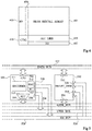
- the figure 1 is a simplified electrical diagram of an example of a system comprising a microprocessor 100 (CPU) and a conventional memory circuit 150 (MEM).
- CPU microprocessor
- MEM memory circuit 150
- the system comprises a data bus 122 (DATA BUS) which connects, for example connects, a data input / output port 102 of the microprocessor 100 to a corresponding data input / output port 152 of the circuit. memory 150.
- DATA BUS data bus 122
- the system further comprises an address bus 124 (ADDR_BUS) which connects, for example connects, an address output port 104 of the microprocessor 100 to a corresponding address input port 154 of the memory circuit 150.
- ADDR_BUS address bus 124
- the system further includes a control bus 126 (CTRL_BUS) which connects, eg connects, a control output port 106 of the microprocessor 100 to a corresponding control input port 156 of the memory circuit 150.
- CTRL_BUS control bus 126
- the control bus 126 allows in particular to activate the memory circuit read or write.
- input port and / or output means here a set of one or more input and / or output conductive terminals for receiving and / or providing a digital signal on one or more bits.
- bus means a set of one or more conductive elements, for example one or more conductive tracks or one or more conductive wires, respectively connecting the terminal or terminals of a port of the microprocessor to the corresponding terminal (s). a memory port, and intended carrying a digital signal on one or more bits of the microprocessor to the memory or vice versa.
- the data and address buses and ports are adapted to transmit signals of several bits in parallel, for example 8 to 64 bits for the data bus and 20 to 60 bits for the address bus. that is to say they each comprise several parallel conductors.
- the bus and the control port may comprise a single conductor (for transmitting a single binary signal), or several parallel conductors (for transmitting a signal of several bits in parallel).
- the microprocessor 100 applies the address of the data to be read to the address input port 154 of the memory circuit (via the address output port 104 of the microprocessor and the bus address 124), and applies a read control signal to the control input port 156 of the memory circuit (via the control output port 106 of the microprocessor and the control bus 126).
- the microprocessor then reads the corresponding data on the data input / output port 152 of the memory circuit (via the data bus 122 and the data input / output port 102 of the microprocessor).
- the microprocessor 100 applies the address of the memory area to be written to the address input port 154 of the memory circuit (via the address output port 104 of the microprocessor and the address bus 124), applies the data to be written to the data input / output port 152 of the memory circuit (via the data input / output port 102 of the microprocessor and the data bus 122), and applies a write control signal on the control input port 156 of the memory circuit (via the control output port 106 of the microprocessor and the control bus 126).
- the microprocessor 100 is adapted to execute a sequence of instructions stored in a specific storage part instructions for the memory circuit 150, for example for carrying out data processing operations stored in another part of the memory circuit 150 or in another memory circuit (not shown) connected to the same address, data and control that the memory circuit 150.
- the microprocessor comprises an instruction decoding circuit 111 (DECODER), an internal memory circuit 112 (REG) comprising or several temporary data storage registers, an instruction counter 113 (PC), and an arithmetic and logic unit 114 (ALU) adapted to implement basic arithmetic and / or logic operations for processing data contained in the internal memory circuit 112.
- the instruction counter 113 is incremented.
- Each instruction is read at the corresponding address of the memory circuit 150, determined according to the state of the instruction counter 113.
- the instruction is then decoded by the instruction decoding circuit 111 of the microprocessor, then executed by the microprocessor, it being understood that the execution of the instruction may or may not include read or write access to the memory circuit 150.
- the figure 2 is a diagram illustrating an example of a method of implementing a calculation operation in the system of the figure 1 . More particularly, it is considered in this example that the internal memory circuit 112 of the microprocessor 100 comprises two data storage registers r0 and r1 (not detailed on the figure 1 ), and it is considered as an illustration the implementation of a calculation instruction of the type "add r0, r1, CST" (in assembler language), of adding to the contents of the register r1 the constant value CST, and to write the result of the addition in the register r0.
- the internal memory circuit 112 of the microprocessor 100 comprises two data storage registers r0 and r1 (not detailed on the figure 1 ), and it is considered as an illustration the implementation of a calculation instruction of the type "add r0, r1, CST" (in assembler language), of adding to the contents of the register r1 the constant value CST, and to write the result of the addition in the register r0.
- the process of figure 2 comprises an initial step 201 (FETCH) for reading the instruction in the memory circuit 150.
- the microprocessor applies to the address input port 154 of the circuit 150 (via the address bus 124) the address of the instruction to be read, determined according to the value of the instruction counter 113.
- the microprocessor simultaneously applies a read control signal to the control input port 156 of the memory circuit 150 (via the control bus 126).
- the instruction, coded in the form of a digital data item, is then read by the microprocessor on the data input / output port 152 of the memory circuit 150 (via the data bus 122).
- the process of figure 2 further comprises a decoding step 203 (DECODE), by the instruction decoding circuit 111 of the microprocessor, of the instruction read in step 201.
- DECODE decoding step 203
- the process of figure 2 further comprises a step 205 (UPDATE_PC) of updating the instruction counter 113, consisting for example of incrementing the counter 113.
- UPDATE_PC UPDATE_PC
- the process of figure 2 furthermore comprises a step 207 (EXE) of execution of the instruction itself, that is to say, for example, execution, by the arithmetic and logic unit 114, of the addition r1 + CST .
- EXE a step 207 of execution of the instruction itself, that is to say, for example, execution, by the arithmetic and logic unit 114, of the addition r1 + CST .
- the process of figure 2 further comprises a step 209 (WRITE_BACK) writing the result of the operation in the register r0.
- the figure 3 is a diagram illustrating an exemplary method of implementing a storage operation in memory of a data item in the system of the figure 1 . More particularly, it is considered, as in the previous example, that the internal memory circuit 112 of the microprocessor 100 comprises two data storage registers r0 and r1, and it is considered as illustrative the implementation of a storage instruction of data type "store r0, r1" (in assembly language), consisting of storing the value contained in the register r1 at the address contained in the register r0.
- the process of figure 3 comprises initial steps 301 (FETCH), 303 (DECODE), 305 (UPDATE_PC) and 307 (EXE) similar or identical to the steps 201, respectively 203, respectively 205, respectively 207 of the method of the figure 2 .
- the values stored in the registers r0 and r1 are respectively applied to the address port 104 and the data port 102 of the microprocessor.
- a write command signal is applied to the control port 106 of the microprocessor.
- the process of figure 3 further comprises a memory access step 309 (ACCESS_MEM) for actually performing the write operation in the memory.
- ACCESS_MEM memory access step 309
- the microprocessor applies to the address input port 154 of the memory circuit 150 (via the address bus 124) the address stored in the register r0 of the internal memory circuit 112, applies to the port d data input / output 152 of the memory circuit 150 (via the data bus 122) the data contained in the register r1, and applies to the control input port 156 of the memory circuit 150 (via the control bus 126) a write control signal.
- the process is similar to that of the figure 3 , except that the steps 307/309 then consist in read access to the memory circuit 150. More particularly, in the step 309, the microprocessor applies to the address input port 154 of the memory circuit 150 (FIG.
- the address stored in the register r0 applies to the control input port 156 of the memory circuit 150 (via the control bus 126) a read command signal and then writes to the register r1 the data read on the input / data output port 152 of the memory circuit 150 (via the data bus 122).
- the figure 4 is a very simplified diagram illustrating, in the form of functional blocks, an example of an embodiment of a memory circuit adapted to implement calculation operations.
- the memory circuit of the figure 4 comprises a matrix 401 (SRAM_BITCELL_ARRAY) of elementary cells, for example SRAM cells.
- the matrix 401 is similar to the matrices described in the French patent application N ° 16/54623 above.
- the memory circuit of the figure 4 further comprises a row select circuit 403 (RS) adapted to select a single row of the array 401 to perform a conventional read or write operation, or to simultaneously select for reading one or more rows of the array 401, so as to implement, on the column output conductive tracks of the matrix, basic logic operations having for operands data stored in the selected rows.
- RS row select circuit 403
- the row selection circuit 403 may comprise a specific register 404 of N bits, where N denotes the number of rows of the matrix 401, adapted to contain an operand selection vector, as will be detailed hereinafter in relation to the Figures 6, 7 and 8 .
- the memory circuit of the figure 4 further comprises a calculation logic circuit 405 (ALU_LIKE) adapted to implement additional calculation operations from the signals read on the conductive column output tracks of the matrix.
- the memory circuit of the figure 4 further comprises an input / output circuit 407 (I / O) connecting the columns of the array to connection terminals outside the memory circuit, for example to a data input / output port (not detailed on the figure 4 ) of the memory circuit.
- the memory circuit of the figure 4 further comprises a control circuit 409 (CTRL) connected to the circuits 403, 405 and 407.
- CTRL control circuit 409
- the figure 5 is a simplified electrical diagram of an example of an embodiment of a system comprising a microprocessor 500 (CPU) and a memory circuit 550 (SMART_MEM) adapted to implement calculation operations, for example a memory circuit of the type described in connection with the figure 4 .
- CPU microprocessor 500
- SMART_MEM memory circuit 550
- the system comprises a data bus 522 (DATA BUS) which connects, for example connected, a data input / output port 502 of the microprocessor 500 to a corresponding data input / output port 552 of the circuit memory 550.
- DATA BUS data bus 522
- the system further comprises an address bus 524 (ADDR_BUS) which connects, for example connects, an address output port 504 of the microprocessor 500 to a corresponding address input port 554 of the memory circuit 550.
- ADDR_BUS address bus 524
- the system further includes a control bus 526 (CTRL_BUS) which connects, eg connects, a control output port 506 of the microprocessor 500 to a corresponding control input port 556 of the memory circuit 550.
- CTRL_BUS control bus 526
- Buses and data ports, addresses and system control of the figure 5 are for example identical or similar to those of the system of the figure 1 .
- the use of these buses and data, address and control ports is however different from the conventional use, so as to allow in particular to control the memory circuit to implement calculation operations.
- the system of figure 5 further comprises an operation mode select bus 528 (SM_BUS) which connects, for example connects, an operating mode select output port 508 of the microprocessor 500 to a corresponding operating mode select input port 558 of the memory circuit 550.
- SM_BUS operation mode select bus 528
- the bus and the operating mode selection ports of the system of the figure 5 comprise a single conductor (for transmitting a single binary signal), or a plurality of parallel conductors (for transmitting a signal of several bits in parallel).
- bus and the ports of selection of mode of operation of the system of the figure 5 have been shown separated from the bus and data ports, addresses and control of the system, the described embodiments are not limited to this particular example.
- the bus and mode selection ports of the system of the figure 5 can correspond to unused bus drivers and data ports, addresses or system control.
- the microprocessor 500 comprises an instruction decoding circuit 511 (DECODER), an internal memory circuit 512 (REG) comprising one or more temporary data storage registers, an instruction counter 513 (PC), and an arithmetic unit. 514 (ALU) logic.
- the circuits 511, 512, 513 and 514 of the microprocessor 500 are for example identical or similar to the circuits 111, respectively 112, respectively 113, respectively 114 of the microprocessor 100 of the figure 1 .
- the microprocessor 500 controls the memory circuit 550 according to a first so-called conventional operating mode. For this, the microprocessor 500 applies an operating mode select signal of a first state or a first value to the operation mode select input port 558 of the memory circuit (via the select output port). operating mode 508 of the microprocessor and the operating mode selection bus 528).
- the signals applied to the bus and address, data and control ports are similar to what has been described in relation to the figure 1 .
- the microprocessor applies the address of the data to be read to the address input port 554 of the memory circuit (via the address output port 504 of the microprocessor and the address bus 524), and applies a read command signal to the control input port 556 of the memory circuit (via the microprocessor control output port 506 and the control bus 526) .
- the microprocessor then reads the corresponding data on the data input / output port 552 of the memory circuit (via the data bus 522 and the data input / output port 502 of the microprocessor).
- the microprocessor For writing a data in the memory circuit, the microprocessor applies the address of the memory area to write to the address input port 554 of the memory circuit (via the address output port 504 of the microprocessor and the address bus 524), applies the data to be written to the data input / output port 552 of the memory circuit (via the data input / output port 502 of the microprocessor and the data bus 522), and applies a control signal write to the control input port 556 of the memory circuit (via the control output port 506 of the microprocessor and the control bus 526).
- the microprocessor 500 controls the memory circuit according to a second so-called intelligent operating mode.
- the microprocessor applies a second or second mode operating mode selection signal to the operating mode selection input port 558 of the memory circuit (via the output selector output port). operating mode 508 of the microprocessor and the operating mode selection bus 528).
- the microprocessor also simultaneously applies an instruction signal to the data input / output port 552 of the memory circuit (via the data input / output port 502 of the microprocessor and the bus 522).
- the microprocessor can further simultaneously apply an address signal to the address input port 554 of the memory circuit (via the address output port 504 of the microprocessor and the address bus 524) to indicate to the circuit memory at which memory location write the result of the calculation operation.
- the internal control circuit of the memory circuit 550 (the circuit 409 of the figure 4 ) is adapted to read the mode select signal applied to the mode select input port 558 of the memory circuit.
- the internal control circuit of the The memory circuit interprets the signals applied to the bus and address, data and control ports as conventional control signals. More particularly, the address signal applied to the address input port 554 is read and decoded (by the control circuit and / or the row selection circuit), and the corresponding row is activated to set implement the read or write operation required.
- the internal control circuit of the memory circuit interprets the signal applied to the data input / output port of the memory circuit as an instruction signal indicating to the memory circuit which calculation operation to execute and in which rows of the memory circuit are the operands of this calculation.
- the instruction signal is read and decoded (by the control circuit and the row selection circuit), and the corresponding rows are activated in reading so as to implement the required calculation operation.
- the result of the calculation operation can be rewritten directly in the memory circuit 550 (without going back through the microprocessor internal memory circuit) to the address indicated on the address input port 554 of the memory circuit.
- An advantage of the system of figure 5 is that it allows conventional access to the memory circuit 550, for example to perform conventional calculation operations by means of the arithmetic and logic unit 504 of the microprocessor 500, and intelligent access to the memory circuit 550, in to perform calculation operations directly within the memory circuit 550 so as to relieve the arithmetic and logic unit 504 of the microprocessor and limit the data exchange between the memory circuit 550 and the microprocessor 500.
- the figure 6 schematically illustrates an exemplary format of an instruction signal used by the microprocessor 500 of the system of the figure 5 , to control the implementation of a calculation operation by the memory circuit 550 of the system.
- the instruction signal represented in figure 6 is a multi-bit signal applied by the microprocessor to the data input / output port 552 of the memory circuit 550.
- This instruction signal comprises a first field OP_CODE on one or more bits, defining the type of logical or arithmetic operation to be performed within the memory circuit.
- the instruction signal further comprises a second field OPERAND_SELECT on several bits, defining the addresses of the rows containing the operands of the operation to be performed.
- a calculation operation implemented within the memory circuit may comprise a high number of operands, for example greater than two, and up to the total number of rows of the memory circuit.
- a problem that arises is the addressing of the data operands.
- the control circuit generally comprises a single row address decoder adapted to receive an address. encoded on log 2 (N) bits, and to activate the corresponding row for a read or write operation in that row.
- K an integer greater than or equal to 2
- K an integer greater than or equal to 2
- one possibility would be to replicate the row address decoder K times. , so as to be able to simultaneously transmit the K address operands to the control circuit during the implementation of a calculation operation.
- the OPERAND_SELCT field of the instruction signal of the figure 6 defines, under coded form, an operand selection vector for identifying the rows to be selected during the implementation of the calculation operation.
- the operand selection vector comprises for example N bits, where N is the number of rows of the memory circuit.
- the operand selection vector is used as a selection mask to activate simultaneously reading a plurality of rows of the memory circuit during the implementation of the calculation operation.
- the corresponding row of the memory circuit is activated in read mode if the corresponding bit of the operand selection vector is at the binary value '1', and n ' is not read-enabled if the corresponding bit of the operand selection vector is at the binary value '0'.
- the OPERAND_SELCT field contains two subfields ADDR and MASK of log 2 (N) bits each, whose combination defines an N-bit operand selection vector.
- the decoding of the OPERAND_SELECT field can be performed within the memory circuit, for example by the row selection circuit of the memory circuit. Once decoded, the row selection vector can be stored in a specific register of the memory circuit in order to activate reading the rows selected during the implementation of the actual calculation operation.
- An exemplary embodiment of a decoding circuit adapted to generate an operand selection vector from the OPERAND_SELECT field will now be described in relation to the figures 7 and 8 .
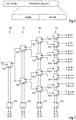
- the figure 7 is a simplified electrical diagram of an exemplary embodiment of a row selection circuit of a memory circuit adapted to implement calculation operations (for example the row selection circuit 403 of FIG. figure 4 ).
- N of selectable rows equal to 16 is considered, it being understood that those skilled in the art will be able to adapt the circuit described to a different number of rows.
- the circuit of the figure 7 comprises first elementary selection logic cells 701 with two inputs a and b and two outputs c and d each, and second elementary selection logic cells 703 with three inputs e, f and g and two outputs h and i each.
- each cell 703 of the stage has its input nodes f and g respectively connected to the output nodes c and d of the cell 701 of the stage.
- the truth table of the cells 701 is as follows (designating the input and output logic signals of a cell 701 by the same references as the corresponding input and output terminals of the cell): at b c d 0 0 0 1 0 1 1 0 1 0 1 1 1 1 1 1 1 1 1
- the truth table of the cells 703 is as follows (designating the input and output logic signals of a cell 703 by the same references as the corresponding input and output terminals of the cell): e f g h i 0 0 0 0 0 0 0 1 0 0 0 0 1 0 0 0 0 0 1 1 0 0 1 0 0 0 0 0 1 0 1 0 1 0 1 0 1 1 1 1 1 1 1 1 1 1 1 1 1 1 1 1 1 1 1 1 1 1 1 1 1 1 1 1 1 1 1 1 1 1 1
- the Q log 2 (N) bits of the MASK subfield of the OPERAND _SELECT field of the instruction signal are respectively applied, in parallel, on the input terminals has cells 701 of the stages E 0 to E Q-1 of the row selection circuit.
- the Q log 2 (N) bits of the ADDR subfield of the OPERAND_SELECT field of the instruction signal are respectively applied, in parallel, to the input terminals b of the cells 701 of the stages E 0 to E Q- 1 of the row selection circuit.
- An activation signal EN in the logic state 1 is furthermore applied to the input terminal e of the cell 703 of the stage E 0 .
- the logic output signals supplied on the terminals h and i of the 2 Q-1 cells 703 of the stage E Q-1 correspond respectively to the N bits R ⁇ 0>, R ⁇ 1>, ... R ⁇ N-1 > a row selection vector R used to decide whether to activate or not read each of the N rows of the matrix during the implementation of the calculation operation.
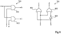
- the figure 8 illustrates in greater detail an exemplary embodiment of an elementary cell 701 (in the right part of the figure 8 ) of the circuit of the figure 7 , and an exemplary embodiment of an elementary cell 703 (in the left part of the figure 8 ) of the circuit of the figure 7 .
- the cell 701 comprises two logic gates OR 801 and 802 with two inputs and one output each.
- the OR gate 801 has a first input connected to the input node a of the cell and a second input connected to the input node b of the cell.
- the OR gate 802 for its part has a first input connected to the input node a of the cell and a second input connected to the input node b of the cell via an inverter 803.
- the output node of the OR gate 801 is connected to the output node c of the cell, and the output node of the OR gate 802 is connected to the output node d of the cell.
- the cell 703 comprises two AND logic gates 811 and 812 with two inputs and one output each.
- the AND gate 811 has a first input connected to the input node e of the cell and a second input connected to the input node f of the cell.
- the AND gate 812 has a first input connected to the input node e of the cell and a second input connected to the input node g of the cell.
- the output node of the AND gate 811 is connected to the output node h of the cell, and the output node of the AND gate 812 is connected to the output node i of the cell.
- the preparation of the control signals of the memory circuit 550 and the transmission of these control signals to the memory circuit 550 can be carried out using only the conventional set of instructions of the microprocessor 550. This is made possible by the fact that the control signals of the memory circuit 550 in intelligent mode pass through the same data bus, address and control than the control signals of the memory circuit 550 in conventional mode.
- the control signals necessary for the implementation of a calculation operation within the memory circuit 550 provision can be made for using a "store r0, r1" type instruction. "(in assembly language), conventionally used to store the value contained in the register r1 at the address of the memory circuit contained in the register r0.
- initial stages of preparation of the registers r0 and r1 of the microprocessor are provided for writing respectively, in the register r1, the instruction signal defining the computation operation to be performed.
- the address to which to write the result of the calculation operation within the memory circuit 550, for example in the format described in connection with the figure 6 , and in the register r0, the address to which to write the result of the calculation operation.
- the preparation of the control signals of the memory circuit 550 and the transmission of these control signals to the memory circuit 550 can be carried out using an instruction specific, in addition to the classic 550 microprocessor instruction set.
- the preparation of the control signals of the memory circuit 550 and the transmission of these control signals to the memory circuit 550 can be carried out using a set specific instruction, comprising for example a specific instruction by type of calculation operation achievable within the memory circuit, the specific set of instructions to be added to the conventional instruction set of the microprocessor 550.
- the first and second variants mentioned above have the advantage of facilitating the work of compiling a code source into a sequence of instructions executable by the microprocessor.
- a disadvantage of these variants lies in their incompatibility with microprocessors not recognizing the specific instructions to the intelligent operating mode of the memory circuit.
- a benefit of the system of figure 5 is that it allows conventional access to the memory circuit 550, for example to perform conventional calculation operations by means of the arithmetic and logic unit 504 of the microprocessor 500, and intelligent access to the memory circuit 550, in to perform calculation operations directly within the memory circuit 550.
- the programmer can take advantage of these two modes of operation. By way of example, it will be able to choose on its own initiative, for each calculation operation, whether it wishes the operation to be carried out conventionally by the arithmetic and logic unit of the microprocessor, or if it wishes that the operation is performed within the memory circuit. Alternatively, this choice can be made automatically by a source code compilation software, so as to optimize the speed of execution of the program and / or the power consumption of the system. In the latter case, the programmer can use a conventional programming language, not allowing to directly choose the desired operating mode for each operation.
- An advantage of the proposed system is that conventional accesses to the memory circuit 550 and intelligent accesses to the memory circuit 550 can be executed interleaved.
- certain instructions sent by the microprocessor 500 to the memory circuit 550 may take several clock cycles of the microprocessor 500 to be executed by the memory circuit 550.
- other conventional instructions or smart can be transmitted to the memory circuit 550 and executed in parallel by the memory circuit 550, for example when they relate to different rows of the memory circuit 550 and / or when the memory is a multiport memory, and / or during cycles during of which the memory 550 is not read or written as part of the execution of the smart instruction.
- the instructions transmitted by the microprocessor 500 to the memory circuit 550 may be pipelined so as to send a conventional or intelligent instruction to the memory circuit 550 at each clock cycle of the microprocessor 500.
- the intelligent mode of operation of the memory circuit can be used to perform operations other than calculation operations.
- the intelligent mode of operation of the memory circuit can be used to perform simultaneous writing of the same data in several rows of the memory.
- the rows to be written can be selected by means of a row selection vector coded according to the coding format described in relation to the Figures 6, 7 and 8 .
- the described embodiments are not limited to the example of an instruction signal format described in relation to the Figures 6, 7 and 8 to control the memory circuit in the intelligent operation mode.
- an operation requiring the selection of a limited number of rows for example an operation requiring the selection of only two rows (for example a computation operation with two operands or a simultaneous write operation d the same data in two rows of the memory circuit)
- one or more additional row addresses to be selected can be transmitted via the address bus.
Abstract
L'invention concerne un circuit mémoire (550) comportant :plusieurs cellules élémentaires de stockage agencées en matrice selon des rangées et des colonnes ;un port d'entrée/sortie de données (552) ;un port d'entrée d'adresses (554) ;un port d'entrée de sélection de mode (558) ; etun circuit interne de commande configuré pour :lire un signal de sélection de mode appliqué sur le port de sélection de mode (558) ;lorsque le signal de sélection de mode est à un premier état, lire une adresse d'une rangée sur le port d'entrée d'adresses (554) et mettre en oeuvre une opération de lecture ou d'écriture dans cette rangée ; etlorsque le signal de sélection de mode est à un deuxième état, lire sur le port d'entrée/sortie de données (552) un signal d'instruction et mettre en oeuvre une opération comprenant l'activation simultanée en lecture ou en écriture d'au moins deux rangées.A memory circuit (550) includes: a plurality of storage element cells arranged in a row and column array, a data input / output port (552), an address input port (554), and ) a mode selection input port (558); andan internal control circuit configured to: read a mode select signal applied to the mode select port (558); when the mode select signal is in a first state, read an address of a row on the port entering an address (554) and performing a read or write operation in that row; andwhen the mode selection signal is in a second state, reading on the data input / output port (552) an instruction signal and performing an operation including simultaneous read or write activation of at least two rows.
Description
La présente demande concerne le domaine des circuits mémoire. Elle vise plus particulièrement un circuit mémoire adapté à mettre en oeuvre des opérations de calcul. Elle vise en outre un système comportant un circuit mémoire adapté à mettre en oeuvre des opérations de calcul et un microprocesseur couplé à ce circuit mémoire.The present application relates to the field of memory circuits. It relates more particularly to a memory circuit adapted to implement calculation operations. It also aims a system comprising a memory circuit adapted to implement calculation operations and a microprocessor coupled to this memory circuit.
Il a déjà été proposé, dans la demande de brevet français N°
La présente demande concerne la problématique de la commande d'un tel circuit mémoire, et, plus particulièrement, de la coopération entre un tel circuit mémoire et un microprocesseur couplé à ce circuit mémoire, notamment pour permettre une utilisation du circuit mémoire à la fois comme mémoire conventionnelle, et comme circuit mémoire intelligente pour mettre en oeuvre des opérations de calcul.The present application relates to the problem of controlling such a memory circuit, and, more particularly, to the cooperation between such a memory circuit and a microprocessor coupled to this memory circuit, in particular to allow use of the memory circuit as both conventional memory, and as intelligent memory circuit for implementing calculation operations.
Ainsi, un mode de réalisation prévoit un circuit mémoire comportant :
- une pluralité de cellules élémentaires de stockage agencées en matrice selon des rangées et des colonnes ;
- un port d'entrée/sortie de données ;
- un port d'entrée d'adresses ;
- un port d'entrée de sélection de mode ; et
- un circuit interne de commande configuré pour :
- lire un signal de sélection de mode appliqué sur le port de sélection de mode ;
- lorsque le signal de sélection de mode est à un premier état, lire une adresse d'une rangée sur le port d'entrée d'adresses et mettre en oeuvre, via le port d'entrée/sortie de données, une opération de lecture ou d'écriture dans cette rangée ; et
- lorsque le signal de sélection de mode est à un deuxième état, lire sur le port d'entrée/sortie de données un signal d'instruction et mettre en oeuvre une opération comprenant l'activation simultanée en lecture ou en écriture d'au moins deux rangées sélectionnées en fonction du signal d'instruction.
- a plurality of elementary storage cells arranged in a matrix in rows and columns;
- a data input / output port;
- an address entry port;
- a mode selection input port; and
- an internal control circuit configured for:
- read a mode select signal applied to the mode select port;
- when the mode select signal is in a first state, read an address from a row on the address input port and implement, via the data input / output port, a read operation or writing in this row; and
- when the mode selection signal is in a second state, reading on the data input / output port an instruction signal and performing an operation including simultaneous read or write activation of at least two rows selected according to the instruction signal.
Selon un mode de réalisation, le circuit interne de commande est adapté à, lorsque le signal de sélection de mode est au deuxième état, mettre en oeuvre une opération de calcul comprenant l'activation simultanée en lecture d'au moins deux rangées sélectionnées en fonction du signal d'instruction.According to one embodiment, the internal control circuit is adapted to, when the mode selection signal is in the second state, implement a calculation operation comprising simultaneously activating in reading at least two rows selected according to the instruction signal.
Selon un mode de réalisation, le circuit interne de commande est en outre configuré pour, lorsque le signal de sélection de mode est au deuxième état, lire un signal d'adresse sur le port d'entrée d'adresses et écrire à l'adresse correspondante du circuit mémoire un résultat de l'opération de calcul.According to one embodiment, the internal control circuit is further configured to, when the mode select signal is in the second state, read an address signal on the address input port and write to the address. corresponding memory circuit a result of the calculation operation.
Selon un mode de réalisation, le circuit interne de commande est adapté à, lorsque le signal de sélection de mode est au deuxième état, mettre en oeuvre une opération d'écriture d'une même donnée dans au moins deux rangées sélectionnées en fonction du signal d'instruction.According to one embodiment, the internal control circuit is adapted to, when the mode selection signal is in the second state, implement an operation for writing the same data in at least two rows selected according to the signal instruction.
Selon un mode de réalisation, le signal d'instruction comprend un premier champ définissant un type d'opération à mettre en oeuvre, et un deuxième champ définissant les adresses des rangées à sélectionner pour la mise en oeuvre de l'opération.According to one embodiment, the instruction signal comprises a first field defining a type of operation to be implemented, and a second field defining the addresses of the rows to be selected for the implementation of the operation.
Selon un mode de réalisation, le deuxième champ comprend un premier sous-champ et un deuxième sous-champ de log2(N) bits chacun, où N est un entier désignant le nombre de rangées de la matrice.According to one embodiment, the second field comprises a first subfield and a second subfield of log 2 (N) bits each, where N is an integer designating the number of rows of the matrix.
Selon un mode de réalisation, le circuit de commande interne comprend un circuit de sélection de rangées adapté à générer un vecteur de sélection de rangées de N bits à partir des premier et deuxième sous-champs du deuxième champ du signal d'instruction.According to one embodiment, the internal control circuit comprises a row selection circuit adapted to generate an N-bit row selection vector from the first and second subfields of the second field of the instruction signal.
Selon un mode de réalisation, le circuit de sélection de rangées comprend Q=log2(N) étages Ej, avec j entier allant de 0 à Q-1, chaque étage Ej comprenant une première cellule logique de sélection comprenant des premier et deuxième noeuds d'entrée et des premier et deuxième noeuds de sortie, et 2j deuxièmes cellules logiques de sélection comprenant chacune des premier, deuxième et troisième noeuds d'entrée et des premier et deuxième noeuds de sortie.According to one embodiment, the row selection circuit comprises Q = log 2 (N) stages E j , where j is an integer ranging from 0 to Q-1, each stage E j comprising a first selection logic cell comprising first and second stages. second input nodes and first and second output nodes, and 2j second selection logic cells each comprising first, second and third input nodes and first and second output nodes.
Selon un mode de réalisation :
- dans chaque étage Ej, chaque deuxième cellule de l'étage a ses deuxième et troisième noeuds d'entrée connectés respectivement aux premier et deuxième noeuds de sortie de la première cellule de l'étage ; et
- dans chaque étage Ej à l'exception de l'étage EQ-1, chaque deuxième cellule de l'étage a son premier noeud de sortie connecté au premier noeud d'entrée de l'une des deuxièmes cellules de l'étage Ej+1 et son deuxième noeud de sortie connecté au premier noeud d'entrée d'une autre des deuxièmes cellules de l'étage Ej+1.
- in each stage E j , each second cell of the stage has its second and third input nodes respectively connected to the first and second output nodes of the first cell of the stage; and
- in each stage E j with the exception of the stage E Q-1 , each second cell of the stage has its first output node connected to the first input node of one of the second cells of the stage E j + 1 and its second output node connected to the first input node of another of the second cells of the stage E j + 1 .
Selon un mode de réalisation :
- chaque première cellule comprend des première et deuxième portes logiques OU, la première porte OU ayant une première entrée connectée au premier noeud d'entrée de la cellule, une deuxième entrée connectée au deuxième noeud d'entrée de la cellule, et une sortie connectée au premier noeud de sortie de la cellule, et la deuxième porte OU ayant une première entrée connecté au premier noeud d'entrée de la cellule, une deuxième entrée reliée au deuxième noeud d'entrée de la cellule par l'intermédiaire d'un inverseur, et une sortie connectée au deuxième noeud de sortie de la cellule ; et
- chaque deuxième cellule comprend des première et deuxième portes logiques ET, la première porte ET ayant une première entrée connectée au premier noeud d'entrée de la cellule, une deuxième entrée connectée au deuxième noeud d'entrée de la cellule, et une sortie connectée au premier noeud de sortie de la cellule, et la deuxième porte ET ayant une première entrée connectée au premier noeud d'entrée de la cellule, une deuxième entrée connectée au troisième noeud d'entrée de la cellule, et une sortie connectée au deuxième noeud de sortie de la cellule.
- each first cell comprises first and second OR logic gates, the first OR gate having a first input connected to the first input node of the cell, a second input connected to the second input node of the cell, and an output connected to the first output node of the cell, and the second OR gate having a first input connected to the first input node of the cell, a second input connected to the second input node of the cell via an inverter, and an output connected to the second output node of the cell; and
- each second cell comprises first and second logic gates AND, the first AND gate having a first input connected to the first input node of the cell, a second input connected to the second input node of the cell, and an output connected to the first output node of the cell, and the second AND gate having a first input connected to the first input node of the cell, a second input connected to the third input node of the cell, and an output connected to the second node of leaving the cell.
Selon un mode de réalisation, le circuit interne de commande est configuré pour, lorsque le signal de sélection de mode est au deuxième état, appliquer les log2(N) bits du premier sous-champ respectivement sur les log2(N) deuxièmes noeuds d'entrée des premières cellules du circuit de sélection de rangées, et appliquer les log2(N) bits du deuxième sous-champ respectivement sur les log2(N) premiers noeuds d'entrée des premières cellules du circuit de sélection de rangées.According to one embodiment, the internal control circuit is configured to, when the mode selection signal is in the second state, apply the log 2 (N) bits of the first subfield respectively to the log 2 (N) second nodes input of the first cells of the row selection circuit, and apply the log2 (N) bits of the second subfield respectively on the log 2 (N) first input nodes of the first cells of the row selection circuit.
Un autre mode de réalisation prévoit un système comportant un microprocesseur et un circuit mémoire tel que défini ci-dessus, le système comportant en outre :
- un bus de données reliant un port d'entrée/sortie de données du microprocesseur au port d'entrée/sortie de données du circuit mémoire ;
- un bus d'adresses reliant un port de sortie d'adresses du microprocesseur au port d'entrée d'adresses du circuit mémoire ; et
- un bus de sélection de mode reliant un port de sortie de sélection de mode du microprocesseur au port d'entrée de sélection de mode du circuit mémoire.
- a data bus connecting a data input / output port of the microprocessor to the data input / output port of the memory circuit;
- an address bus connecting a microprocessor address output port to the address input port of the memory circuit; and
- a mode select bus connecting a microprocessor mode select output port to the mode select input port of the memory circuit.
Selon un mode de réalisation, le microprocesseur est configuré pour :
- dans un premier mode de fonctionnement :
- appliquer un signal de sélection de mode au premier état sur le bus de sélection de mode ;
- appliquer un signal d'adresse de rangée sur le bus d'adresses ; et
- lire ou écrire une donnée dans la rangée correspondante du circuit mémoire via le bus de données, et
- dans un deuxième mode de fonctionnement :
- appliquer un signal de sélection de mode au deuxième état sur le bus de sélection de mode ; et
- appliquer un signal d'instruction sur le bus de données.
- in a first mode of operation:
- applying a mode select signal to the first state on the mode select bus;
- apply a row address signal on the address bus; and
- read or write data in the corresponding row of the memory circuit via the data bus, and
- in a second mode of operation:
- applying a mode select signal to the second state on the mode select bus; and
- apply an instruction signal on the data bus.
Ces caractéristiques et avantages, ainsi que d'autres, seront exposés en détail dans la description suivante de modes de réalisation particuliers faite à titre non limitatif en relation avec les figures jointes parmi lesquelles :
- la
figure 1 est un schéma électrique simplifié d'un système comportant un microprocesseur et un circuit mémoire ; - la
figure 2 est un diagramme illustrant un exemple de mise en oeuvre d'une opération de calcul conventionnelle dans le système de lafigure 1 ; - la
figure 3 est un diagramme illustrant un exemple de mise en oeuvre d'une opération de stockage et de lecture conventionnelle dans le système de lafigure 1 ; - la
figure 4 est un schéma bloc simplifié d'un exemple d'un mode de réalisation d'un circuit mémoire adapté à mettre en oeuvre des opérations de calcul ; - la
figure 5 est un schéma électrique simplifié d'un exemple d'un mode de réalisation d'un système comportant un microprocesseur et un circuit mémoire adapté à mettre en oeuvre des opérations de calcul ; - la
figure 6 illustre schématiquement un exemple de format d'un signal d'instruction utilisé par le microprocesseur pour commander le circuit mémoire dans le système de lafigure 5 ; - la
figure 7 est un schéma électrique simplifié d'un exemple d'un circuit de sélection de rangées d'un circuit mémoire adapté à mettre en oeuvre des opérations de calcul ; et - la
figure 8 illustre plus en détail un exemple de réalisation de cellules de sélection élémentaires du circuit de sélection de rangées de lafigure 8 .
- the
figure 1 is a simplified circuit diagram of a system comprising a microprocessor and a memory circuit; - the
figure 2 is a diagram illustrating an example of implementation of a conventional calculation operation in the system of thefigure 1 ; - the
figure 3 is a diagram illustrating an example of implementing a conventional storage and reading operation in the system of thefigure 1 ; - the
figure 4 is a simplified block diagram of an example of an embodiment of a memory circuit adapted to implement calculation operations; - the
figure 5 is a simplified electrical diagram of an example of an embodiment of a system comprising a microprocessor and a memory circuit adapted to implement calculation operations; - the
figure 6 schematically illustrates an exemplary format of an instruction signal used by the microprocessor to control the memory circuit in the system of thefigure 5 ; - the
figure 7 is a simplified electrical diagram of an example of a row selection circuit of a memory circuit adapted to perform calculation operations; and - the
figure 8 illustrates in greater detail an exemplary embodiment of selection cells elementary row selection circuit of thefigure 8 .
De mêmes éléments ont été désignés par de mêmes références dans les différentes figures. Par souci de clarté, seuls les éléments utiles à la compréhension des modes de réalisation décrits ont été représentés et sont détaillés. En particulier, la réalisation complète d'un circuit mémoire adapté à mettre en oeuvre des opérations de calcul par activation simultanée en lecture d'une pluralité de rangées d'une matrice de cellules élémentaires n'a pas été détaillée, les modes de réalisation décrits étant compatibles avec les architectures connues de tels circuits, et notamment celles décrites dans la demande de brevet français N°
La
Dans cet exemple, le système comprend un bus de données 122 (DATA BUS) qui relie, par exemple connecte, un port d'entrée/sortie de données 102 du microprocesseur 100 à un port d'entrée/sortie de données correspondant 152 du circuit mémoire 150.In this example, the system comprises a data bus 122 (DATA BUS) which connects, for example connects, a data input /
Le système comprend de plus un bus d'adresses 124 (ADDR_BUS) qui relie, par exemple connecte, un port de sortie d'adresses 104 du microprocesseur 100 à un port d'entrée d'adresses correspondant 154 du circuit mémoire 150.The system further comprises an address bus 124 (ADDR_BUS) which connects, for example connects, an
Le système comprend en outre un bus de contrôle 126 (CTRL_BUS) qui relie, par exemple connecte, un port de sortie de contrôle 106 du microprocesseur 100 à un port d'entrée de contrôle correspondant 156 du circuit mémoire 150. Le bus de contrôle 126 permet notamment d'activer le circuit mémoire en lecture ou en écriture.The system further includes a control bus 126 (CTRL_BUS) which connects, eg connects, a
Par port d'entrée et/ou de sortie, on entend ici un ensemble d'une ou plusieurs bornes conductrices d'entrée et/ou de sortie destiné à recevoir et/ou à fournir un signal numérique sur un ou plusieurs bits. De plus, on entend par bus un ensemble d'un ou plusieurs éléments conducteurs, par exemple une ou plusieurs pistes conductrices ou un ou plusieurs fils conducteurs, reliant respectivement la ou les bornes d'un port du microprocesseur à la ou les bornes correspondantes d'un port de la mémoire, et destiné à transporter un signal numérique sur un ou plusieurs bits du microprocesseur à la mémoire ou inversement.By input port and / or output means here a set of one or more input and / or output conductive terminals for receiving and / or providing a digital signal on one or more bits. In addition, bus means a set of one or more conductive elements, for example one or more conductive tracks or one or more conductive wires, respectively connecting the terminal or terminals of a port of the microprocessor to the corresponding terminal (s). a memory port, and intended carrying a digital signal on one or more bits of the microprocessor to the memory or vice versa.
En pratique, les bus et ports de données et d'adresses sont adaptés à transmettre des signaux de plusieurs bits en parallèle, par exemple 8 à 64 bits pour le bus de données et 20 à 60 bits pour le bus d'adresses, c'est-à-dire qu'ils comprennent chacun plusieurs conducteurs parallèles. Le bus et le port de contrôle peuvent quant à eux, selon les architectures, comporter un unique conducteur (permettant de transmettre un signal binaire unique), ou plusieurs conducteurs parallèles (permettant de transmettre un signal de plusieurs bits en parallèle).In practice, the data and address buses and ports are adapted to transmit signals of several bits in parallel, for example 8 to 64 bits for the data bus and 20 to 60 bits for the address bus. that is to say they each comprise several parallel conductors. Depending on the architectures, the bus and the control port may comprise a single conductor (for transmitting a single binary signal), or several parallel conductors (for transmitting a signal of several bits in parallel).
Pour lire une donnée dans le circuit mémoire 150, le microprocesseur 100 applique l'adresse de la donnée à lire sur le port d'entrée d'adresses 154 du circuit mémoire (via le port de sortie d'adresses 104 du microprocesseur et le bus d'adresses 124), et applique un signal de commande en lecture sur le port d'entrée de contrôle 156 du circuit mémoire (via le port de sortie de contrôle 106 du microprocesseur et le bus de contrôle 126). Le microprocesseur lit ensuite la donnée correspondante sur le port d'entrée/sortie de données 152 du circuit mémoire (via le bus de données 122 et le port d'entrée/sortie de données 102 du microprocesseur).To read data in the
Pour écrire une donnée dans le circuit mémoire 150, le microprocesseur 100 applique l'adresse de la zone mémoire à écrire sur le port d'entrée d'adresses 154 du circuit mémoire (via le port de sortie d'adresses 104 du microprocesseur et le bus d'adresses 124), applique la donnée à écrire sur le port d'entrée/sortie de données 152 du circuit mémoire (via le port d'entrée/sortie de données 102 du microprocesseur et le bus de données 122), et applique un signal de commande en écriture sur le port d'entrée de contrôle 156 du circuit mémoire (via le port de sortie de contrôle 106 du microprocesseur et le bus de contrôle 126) .To write data to the
Le microprocesseur 100 est adapté à exécuter une suite d'instructions mémorisée dans une partie spécifique de stockage d'instructions du circuit mémoire 150, par exemple en vue de réaliser des opérations de traitement de données mémorisées dans une autre partie du circuit mémoire 150 ou dans un autre circuit mémoire (non représenté) relié aux mêmes bus d'adresses, de données et de contrôle que le circuit mémoire 150.The
Pour cela, dans l'exemple de la
La
Le procédé de la
Le procédé de la
Le procédé de la
Le procédé de la
Le procédé de la
La
Le procédé de la
Le procédé de la
Pour mettre en oeuvre une opération de chargement d'une donnée stockée dans le circuit mémoire, par exemple une opération de type "load r0, r1" (en langage assembleur), consistant à écrire dans le registre r1 la valeur stockée dans le circuit mémoire à l'adresse contenue dans le registre r0, le procédé est similaire à celui de la
La
La
Dans cet exemple, le système comprend un bus de données 522 (DATA BUS) qui relie, par exemple connecte, un port d'entrée/sortie de données 502 du microprocesseur 500 à un port d'entrée/sortie de données correspondant 552 du circuit mémoire 550.In this example, the system comprises a data bus 522 (DATA BUS) which connects, for example connected, a data input /
Le système comprend de plus un bus d'adresses 524 (ADDR_BUS) qui relie, par exemple connecte, un port de sortie d'adresses 504 du microprocesseur 500 à un port d'entrée d'adresses correspondant 554 du circuit mémoire 550.The system further comprises an address bus 524 (ADDR_BUS) which connects, for example connects, an
Le système comprend en outre un bus de contrôle 526 (CTRL_BUS) qui relie, par exemple connecte, un port de sortie de contrôle 506 du microprocesseur 500 à un port d'entrée de contrôle correspondant 556 du circuit mémoire 550.The system further includes a control bus 526 (CTRL_BUS) which connects, eg connects, a
Les bus et ports de données, d'adresses et de contrôle du système de la
Le système de la
A titre d'exemple, le bus et les ports de sélection de mode de fonctionnement du système de la
Bien que le bus et les ports de sélection de mode de fonctionnement du système de la
Le microprocesseur 500 comprend un circuit de décodage d'instructions 511 (DECODER), un circuit mémoire interne 512 (REG) comprenant un ou plusieurs registres de stockage temporaire de données, un compteur d'instructions 513 (PC), et une unité arithmétique et logique 514 (ALU). Les circuits 511, 512, 513 et 514 du microprocesseur 500 sont par exemple identiques ou similaires aux circuits 111, respectivement 112, respectivement 113, respectivement 114 du microprocesseur 100 de la
Pour lire ou écrire une donnée dans le circuit mémoire 550, le microprocesseur 500 commande le circuit mémoire 550 selon un premier mode de fonctionnement dit classique. Pour cela, le microprocesseur 500 applique un signal de sélection de mode de fonctionnement d'un premier état ou d'une première valeur sur le port d'entrée de sélection de mode de fonctionnement 558 du circuit mémoire (via le port de sortie de sélection de mode de fonctionnement 508 du microprocesseur et le bus de sélection de mode de fonctionnement 528). Les signaux appliqués sur les bus et ports d'adresses, de données et de contrôle sont quant à eux similaires à ce qui a été décrit en relation avec la
Pour réaliser une opération de calcul directement au sein du circuit mémoire 550, le microprocesseur 500 commande le circuit mémoire selon un deuxième mode de fonctionnement dit intelligent. Pour cela, le microprocesseur applique un signal de sélection de mode de fonctionnement d'un deuxième état ou d'une deuxième valeur sur le port d'entrée de sélection de mode de fonctionnement 558 du circuit mémoire (via le port de sortie de sélection de mode de fonctionnement 508 du microprocesseur et le bus de sélection de mode de fonctionnement 528). Le microprocesseur applique en outre simultanément un signal d'instruction sur le port d'entrée/sortie de données 552 du circuit mémoire (via le port d'entrée/sortie de données 502 du microprocesseur et le bus 522). Le microprocesseur peut en outre appliquer simultanément un signal d'adresse sur le port d'entrée d'adresses 554 du circuit mémoire (via le port de sortie d'adresses 504 du microprocesseur et le bus d'adresses 524), pour indiquer au circuit mémoire à quel emplacement mémoire écrire le résultat de l'opération de calcul.To perform a calculation operation directly within the
Le circuit de contrôle interne du circuit mémoire 550 (le circuit 409 de la
Lorsque le signal de sélection de mode de fonctionnement est dans le premier état, correspondant au mode de fonctionnement classique du circuit mémoire, le circuit de contrôle interne du circuit mémoire interprète les signaux appliqués sur les bus et ports d'adresses, de données et de contrôle comme des signaux de commande classique. Plus particulièrement, le signal d'adresse appliqué sur le port d'entrée d'adresses 554 est lu et décodé (par le circuit de contrôle et/ou le circuit de sélection de rangées), et la rangée correspondante est activée de façon à mettre en oeuvre l'opération de lecture ou d'écriture requise.When the operating mode selection signal is in the first state, corresponding to the conventional operating mode of the memory circuit, the internal control circuit of the The memory circuit interprets the signals applied to the bus and address, data and control ports as conventional control signals. More particularly, the address signal applied to the
Lorsque le signal de sélection de mode de fonctionnement est dans le deuxième état, correspondant au mode de fonctionnement intelligent du circuit mémoire, le circuit de contrôle interne du circuit mémoire interprète le signal appliqué sur le port d'entrée/sortie de données du circuit mémoire comme un signal d'instruction indiquant au circuit mémoire quelle opération de calcul exécuter et dans quelles rangées du circuit mémoire se situent les opérandes de ce calcul. Le signal d'instruction est lu et décodé (par le circuit de contrôle et le circuit de sélection de rangées), et les rangées correspondantes sont activées en lecture de façon à mettre en oeuvre l'opération de calcul requise. Le résultat de l'opération de calcul peut être réécrit directement dans le circuit mémoire 550 (sans repasser par le circuit mémoire interne du microprocesseur), à l'adresse indiquée sur le port d'entrée d'adresses 554 du circuit mémoire.When the operating mode selection signal is in the second state, corresponding to the intelligent operating mode of the memory circuit, the internal control circuit of the memory circuit interprets the signal applied to the data input / output port of the memory circuit as an instruction signal indicating to the memory circuit which calculation operation to execute and in which rows of the memory circuit are the operands of this calculation. The instruction signal is read and decoded (by the control circuit and the row selection circuit), and the corresponding rows are activated in reading so as to implement the required calculation operation. The result of the calculation operation can be rewritten directly in the memory circuit 550 (without going back through the microprocessor internal memory circuit) to the address indicated on the
Un avantage du système de la
la
the
Le signal d'instructions représenté en
Ce signal d'instruction comprend un premier champ OP_CODE sur un ou plusieurs bits, définissant le type d'opération logique ou arithmétique à réaliser au sein du circuit mémoire.This instruction signal comprises a first field OP_CODE on one or more bits, defining the type of logical or arithmetic operation to be performed within the memory circuit.
Le signal d'instruction comprend en outre un deuxième champ OPERAND_SELECT sur plusieurs bits, définissant les adresses des rangées contenant les opérandes de l'opération à réaliser.The instruction signal further comprises a second field OPERAND_SELECT on several bits, defining the addresses of the rows containing the operands of the operation to be performed.
On notera qu'une opération de calcul mise en oeuvre au sein du circuit mémoire peut comporter un nombre d'opérandes élevé, par exemple supérieur à deux, et pouvant aller jusqu'au nombre total de rangées du circuit mémoire. Un problème qui se pose est celui de l'adressage des données opérandes. En effet, dans un circuit mémoire classique de N rangées, où N est un entier supérieur ou égal à 2 (par exemple une puissance de 2), le circuit de contrôle comprend généralement un décodeur d'adresse de rangée unique adapté à recevoir une adresse codée sur log2(N) bits, et à activer la rangée correspondante en vue d'une opération de lecture ou d'écriture dans cette rangée. Pour permettre d'activer simultanément en lecture K rangées distinctes de la matrice de façon à réaliser une opération logique à K opérandes, où K est un entier supérieur ou égal à 2, une possibilité serait de répliquer K fois le décodeur d'adresse de rangée, de façon à pouvoir transmettre simultanément les K adresses d'opérandes au circuit de contrôle lors de la mise en oeuvre d'une opération de calcul. Cette solution implique toutefois une augmentation importante de la surface et de la consommation énergétique du circuit mémoire, et n'est en pratique pas compatible avec les dimensions usuelles des bus reliant un circuit mémoire à un microprocesseur, notamment lorsque le nombre d'opérandes K est important (par exemple K = N) .Note that a calculation operation implemented within the memory circuit may comprise a high number of operands, for example greater than two, and up to the total number of rows of the memory circuit. A problem that arises is the addressing of the data operands. In fact, in a conventional memory circuit of N rows, where N is an integer greater than or equal to 2 (for example a power of 2), the control circuit generally comprises a single row address decoder adapted to receive an address. encoded on log 2 (N) bits, and to activate the corresponding row for a read or write operation in that row. To make it possible to activate at the same time K distinct rows of the matrix so as to perform a logical operation with K operands, where K is an integer greater than or equal to 2, one possibility would be to replicate the row address decoder K times. , so as to be able to simultaneously transmit the K address operands to the control circuit during the implementation of a calculation operation. This solution, however, involves a significant increase in the area and the energy consumption of the memory circuit, and is in practice not compatible with the usual dimensions of the bus connecting a memory circuit to a microprocessor, especially when the number of operands K is important (eg K = N).
Ainsi, dans un mode de réalisation préféré, le champ OPERAND_SELCT du signal d'instruction de la
A titre d'exemple, le champ OPERAND_SELCT contient deux sous-champs ADDR et MASK de log2(N) bits chacun, dont la combinaison définit un vecteur de sélection d'opérandes de N bits.By way of example, the OPERAND_SELCT field contains two subfields ADDR and MASK of log 2 (N) bits each, whose combination defines an N-bit operand selection vector.
Le décodage du champ OPERAND_SELECT peut être réalisé au sein du circuit mémoire, par exemple par le circuit de sélection de rangées du circuit mémoire. Une fois décodé, le vecteur de sélection de rangées peut être stocké dans un registre spécifique du circuit mémoire en vue d'activer en lecture les rangées sélectionnées lors de la mise en oeuvre de l'opération de calcul proprement dite. Un exemple de réalisation d'un circuit de décodage adapté à générer un vecteur de sélection d'opérandes à partir du champ OPERAND_SELECT va maintenant être décrit en relation avec les
La
On considère dans cet exemple un nombre N de rangées sélectionnables égal à 16, étant entendu que l'homme du métier saura adapter le circuit décrit à un nombre de rangées différent.In this example, a number N of selectable rows equal to 16 is considered, it being understood that those skilled in the art will be able to adapt the circuit described to a different number of rows.
Le circuit de la
Plus particulièrement, le circuit de la
Dans chaque étage Ej, chaque cellule 703 de l'étage a ses noeuds d'entrée f et g connectés respectivement aux noeuds de sortie c et d de la cellule 701 de l'étage.In each stage E j , each
De plus, dans chaque étage Ej à l'exception de l'étage EQ-1, chaque cellule 703 de l'étage a son noeud de sortie h connecté au noeud d'entrée e de l'une des cellules 703 de l'étage Ej+1 et son noeud de sortie i connecté au noeud d'entrée e d'une autre des cellules 703 de l'étage Ej+1, étant entendu que :
- dans chaque étage Ej à l'exception de l'étage EQ-1, chaque cellule 703 de l'étage a son noeud de sortie h connecté au noeud d'entrée e d'une et d'une seule cellule 703 de l'étage Ej+1 et a son noeud de sortie i connecté au noeud d'entrée e d'une et une seule cellule 703 de l'étage Ej+1 ; et
- dans chaque étage Ej à l'exception de l'étage E0, chacune des cellules 703 de l'étage a son noeud d'entrée e connecté à un et un seul noeud de sortie h ou i d'une cellule 703 de l'étage Ej-1.
- in each stage E j with the exception of the stage E Q-1 , each
cell 703 of the stage has its output node h connected to the input node e of one and asingle cell 703 of the stage E j + 1 and has its output node i connected to the input node e of one and only onecell 703 of the stage E j + 1 ; and - in each stage E j with the exception of the stage E 0 , each of the
cells 703 of the stage has its input node e connected to one and only one output node h or i of acell 703 of the floor E j-1 .
La table de vérité des cellules 701 est la suivante (en désignant les signaux logiques d'entrée et de sortie d'une cellule 701 par les mêmes références que les bornes d'entrée et de sortie correspondantes de la cellule) :
La table de vérité des cellules 703 est la suivante (en désignant les signaux logiques d'entrée et de sortie d'une cellule 703 par les mêmes références que les bornes d'entrée et de sortie correspondantes de la cellule) :
Le fonctionnement du circuit de la
Lors de la mise en oeuvre d'une opération de calcul au sein du circuit mémoire, les Q=log2(N) bits du sous-champ MASK du champ OPERAND _SELECT du signal d'instruction sont appliqués respectivement, en parallèle, sur les bornes d'entrée a des cellules 701 des étages E0 à EQ-1 du circuit de sélection de rangées. De plus, les Q=log2(N) bits du sous-champ ADDR du champ OPERAND_SELECT du signal d'instruction sont appliqués respectivement, en parallèle, sur les bornes d'entrée b des cellules 701 des étages E0 à EQ-1 du circuit de sélection de rangées. Un signal d'activation EN à l'état logique 1 est en outre appliqué sur la borne d'entrée e de la cellule 703 de l'étage E0. Les signaux logiques de sortie fournis sur les bornes h et i des 2Q-1 cellules 703 de l'étage EQ-1 correspondent respectivement aux N bits R<0>, R<1>, ... R<N-1> d'un vecteur de sélection de rangées R utilisé pour décider d'activer ou non en lecture chacune des N rangées de la matrice lors de la mise en oeuvre de l'opération de calcul.When implementing a calculation operation within the memory circuit, the Q = log 2 (N) bits of the MASK subfield of the OPERAND _SELECT field of the instruction signal are respectively applied, in parallel, on the input terminals has
La
Dans cet exemple, la cellule 701 comprend deux portes logiques OU 801 et 802 à deux entrées et un sortie chacune. La porte OU 801 a une première entrée connectée au noeud d'entrée a de la cellule et une deuxième entrée connectée au noeud d'entrée b de la cellule. La porte OU 802 a quant à elle une première entrée connecté au noeud d'entrée a de la cellule et une deuxième entrée reliée au noeud d'entrée b de la cellule par l'intermédiaire d'un inverseur 803. Le noeud de sortie de la porte OU 801 est connectée au noeud de sortie c de la cellule, et le noeud de sortie de la porte OU 802 est connecté au noeud de sortie d de la cellule.In this example, the
Dans cet exemple, la cellule 703 comprend deux portes logiques ET 811 et 812 à deux entrées et une sortie chacune. La porte ET 811 a une première entrée connectée au noeud d'entrée e de la cellule et une deuxième entrée connectée au noeud d'entrée f de la cellule. La porte ET 812 a quant à elle une première entrée connectée au noeud d'entrée e de la cellule et une deuxième entrée connectée au noeud d'entrée g de la cellule. Le noeud de sortie de la porte ET 811 est connecté au noeud de sortie h de la cellule, et le noeud de sortie de la porte ET 812 est connecté au noeud de sortie i de la cellule.In this example, the
De façon avantageuse, lors de la mise en oeuvre d'une opération de calcul au sein du circuit mémoire 550, la préparation des signaux de commande du circuit mémoire 550 et la transmission de ces signaux de commande au circuit mémoire 550 peuvent être réalisées en utilisant uniquement le jeu d'instructions classique du microprocesseur 550. Ceci est rendu possible par le fait que les signaux de commande du circuit mémoire 550 en mode intelligent transitent par les mêmes bus de données, d'adresses et de contrôle que les signaux de commande du circuit mémoire 550 en mode classique.Advantageously, during the implementation of a calculation operation within the
A titre d'exemple, pour transmettre au circuit mémoire 550 les signaux de commande nécessaires à la mise en oeuvre d'une opération de calcul au sein du circuit mémoire 550, on peut prévoir d'utiliser une instruction de type "store r0, r1" (en langage assembleur), classiquement utilisée pour stocker la valeur contenue dans le registre r1 à l'adresse du circuit mémoire contenue dans le registre r0. Avant l'exécution de l'instruction "store" proprement dite, on prévoit des étapes initiales de préparation des registres r0 et r1 du microprocesseur pour écrire respectivement, dans le registre r1, le signal d'instruction définissant l'opération de calcul à réaliser au sein du circuit mémoire 550, par exemple au format décrit en relation avec la
Un avantage de ce mode de fonctionnement réside dans sa compatibilité avec les microprocesseurs existants.An advantage of this mode of operation lies in its compatibility with existing microprocessors.
A titre de première variante, pour mettre en oeuvre une opération de calcul au sein du circuit mémoire 550, la préparation des signaux de commande du circuit mémoire 550 et la transmission de ces signaux de commande au circuit mémoire 550 peuvent être réalisées en utilisant une instruction spécifique, venant s'ajouter au jeu d'instructions classique du microprocesseur 550.As a first variant, to implement a calculation operation in the
A titre de deuxième variante, pour mettre en oeuvre une opération de calcul au sein du circuit mémoire 550, la préparation des signaux de commande du circuit mémoire 550 et la transmission de ces signaux de commande au circuit mémoire 550 peuvent être réalisées en utilisant un jeu d'instructions spécifique, comprenant par exemple une instruction spécifique par type d'opération de calcul réalisable au sein du circuit mémoire, le jeu d'instructions spécifique venant s'ajouter au jeu d'instructions classique du microprocesseur 550.As a second variant, in order to implement a calculation operation within the
Les première et deuxième variantes susmentionnées ont pour avantage de faciliter le travail de compilation d'un code source en une suite d'instructions exécutable par le microprocesseur. Toutefois, un inconvénient de ces variantes réside dans leur incompatibilité avec les microprocesseurs ne reconnaissant pas les instructions spécifiques au mode de fonctionnement intelligent du circuit mémoire.The first and second variants mentioned above have the advantage of facilitating the work of compiling a code source into a sequence of instructions executable by the microprocessor. However, a disadvantage of these variants lies in their incompatibility with microprocessors not recognizing the specific instructions to the intelligent operating mode of the memory circuit.
Comme expliqué ci-dessus, un avantage du système de la
Lors de la programmation d'un logiciel destiné à être exécuté dans un tel système, le programmeur pourra tirer profit de ces deux modes de fonctionnement. A titre d'exemple, il pourra choisir de sa propre initiative, pour chaque opération de calcul, s'il souhaite que l'opération soit réalisée de façon conventionnelle par l'unité arithmétique et logique du microprocesseur, ou s'il souhaite que l'opération soit réalisée au sein du circuit mémoire. A titre de variante, ce choix peut être réalisé de façon automatique par un logiciel de compilation de code source, de façon à optimiser la vitesse d'exécution du programme et/ou la consommation électrique du système. Dans ce dernier cas, le programmeur peut utiliser un langage de programmation classique, ne permettant pas de choisir directement le mode de fonctionnement souhaité pour chaque opération.When programming software intended to be executed in such a system, the programmer can take advantage of these two modes of operation. By way of example, it will be able to choose on its own initiative, for each calculation operation, whether it wishes the operation to be carried out conventionally by the arithmetic and logic unit of the microprocessor, or if it wishes that the operation is performed within the memory circuit. Alternatively, this choice can be made automatically by a source code compilation software, so as to optimize the speed of execution of the program and / or the power consumption of the system. In the latter case, the programmer can use a conventional programming language, not allowing to directly choose the desired operating mode for each operation.
Un avantage du système proposé est que des accès classiques au circuit mémoire 550 et des accès intelligents au circuit mémoire 550 peuvent être exécutés de façon entrelacée. On notera que, dans le mode de fonctionnement intelligent, certaines instructions envoyées par le microprocesseur 500 au circuit mémoire 550 peuvent prendre plusieurs cycles d'horloge du microprocesseur 500 pour être exécutées par le circuit mémoire 550. Lorsqu'une telle instruction est en cours d'exécution par le circuit mémoire 500, d'autres instructions classiques ou intelligentes peuvent être transmises au circuit mémoire 550 et exécutées en parallèle par le circuit mémoire 550, par exemple lorsqu'elles concernent des rangées différentes du circuit mémoire 550 et/ou lorsque la mémoire est une mémoire multiports, et/ou lors de cycles au cours desquels la mémoire 550 n'est pas lue ou écrite dans le cadre de l'exécution de l'instruction intelligente. A titre d'exemple, les instructions transmises par le microprocesseur 500 au circuit mémoire 550 peuvent être pipelinées de façon à envoyer une instruction classique ou intelligente au circuit mémoire 550 à chaque cycle d'horloge du microprocesseur 500.An advantage of the proposed system is that conventional accesses to the
Des modes de réalisation particuliers ont été décrits. Diverses variantes et modifications apparaîtront à l'homme de l'art. En particulier, le mode de fonctionnement intelligent du circuit mémoire peut être utilisé pour réaliser des opérations autres que des opérations de calcul. A titre d'exemple, le mode de fonctionnement intelligent du circuit mémoire peut être utilisé pour réaliser une écriture simultanée d'une même donnée dans plusieurs rangées de la mémoire. Dans ce cas, les rangées à écrire peuvent être sélectionnées au moyen d'un vecteur de sélection de rangées codé selon le format de codage décrit en relation avec les
Par ailleurs, les modes de réalisation décrits ne se limitent pas à l'exemple de format de signal d'instruction décrit en relation avec les
En outre, les modes de réalisation décrits ne se limitent pas à l'exemple de circuit de sélection de rangées décrit en relation avec les
Claims (14)
Applications Claiming Priority (1)
| Application Number | Priority Date | Filing Date | Title |
|---|---|---|---|
| FR1762468A FR3075444B1 (en) | 2017-12-19 | 2017-12-19 | SYSTEM INCLUDING A MEMORY ADAPTED TO IMPLEMENT CALCULATION OPERATIONS |
Publications (1)
| Publication Number | Publication Date |
|---|---|
| EP3503103A1 true EP3503103A1 (en) | 2019-06-26 |
Family
ID=62597551
Family Applications (1)
| Application Number | Title | Priority Date | Filing Date |
|---|---|---|---|
| EP18213223.3A Pending EP3503103A1 (en) | 2017-12-19 | 2018-12-17 | System comprising a memory suitable for performing computing operations |
Country Status (3)
| Country | Link |
|---|---|
| US (1) | US10872642B2 (en) |
| EP (1) | EP3503103A1 (en) |
| FR (1) | FR3075444B1 (en) |
Cited By (5)
| Publication number | Priority date | Publication date | Assignee | Title |
|---|---|---|---|---|
| WO2022029026A1 (en) | 2020-08-04 | 2022-02-10 | Commissariat A L'energie Atomique Et Aux Energies Alternatives | Reconfigurable memory module designed to implement computing operations |
| EP4020475A1 (en) | 2020-12-28 | 2022-06-29 | Commissariat à l'Energie Atomique et aux Energies Alternatives | Memory module suitable for performing computing functions |
| EP4036916A1 (en) | 2021-01-29 | 2022-08-03 | Commissariat à l'Energie Atomique et aux Energies Alternatives | Device comprising a non-volatile memory circuit |
| FR3131428A1 (en) | 2021-12-29 | 2023-06-30 | Commissariat à l'Energie Atomique et aux Energies Alternatives | Direct data transfer system |
| FR3131429A1 (en) | 2021-12-29 | 2023-06-30 | Commissariat à l'Energie Atomique et aux Energies Alternatives | Direct data transfer system |
Citations (3)
| Publication number | Priority date | Publication date | Assignee | Title |
|---|---|---|---|---|
| US20090141537A1 (en) * | 2007-12-03 | 2009-06-04 | Igor Arsovski | Apparatus and method for implementing memory array device with built in computational capability |
| WO2016144726A1 (en) * | 2015-03-12 | 2016-09-15 | Micron Technology, Inc. | Apparatuses and methods for data movement |
| EP3252774A1 (en) * | 2016-05-24 | 2017-12-06 | Commissariat à l'Energie Atomique et aux Energies Alternatives | Memory circuit suitable for performing computing operations |
Family Cites Families (7)
| Publication number | Priority date | Publication date | Assignee | Title |
|---|---|---|---|---|
| US9697877B2 (en) * | 2015-02-05 | 2017-07-04 | The Board Of Trustees Of The University Of Illinois | Compute memory |
| US9921777B2 (en) * | 2015-06-22 | 2018-03-20 | Micron Technology, Inc. | Apparatuses and methods for data transfer from sensing circuitry to a controller |
| KR102548591B1 (en) * | 2016-05-30 | 2023-06-29 | 삼성전자주식회사 | Semiconductor memory device and operation method thereof |
| US10908820B2 (en) * | 2017-09-14 | 2021-02-02 | Samsung Electronics Co., Ltd. | Host-based and client-based command scheduling in large bandwidth memory systems |
| US10497424B2 (en) * | 2017-12-06 | 2019-12-03 | Micron Technology, Inc. | Systems and methods for plate voltage regulation during memory array access |
| US10402116B2 (en) * | 2017-12-11 | 2019-09-03 | Micron Technology, Inc. | Systems and methods for writing zeros to a memory array |
| KR20200013461A (en) * | 2018-07-30 | 2020-02-07 | 삼성전자주식회사 | Performing internal processing operations of memory device |
-
2017
- 2017-12-19 FR FR1762468A patent/FR3075444B1/en active Active
-
2018
- 2018-12-17 EP EP18213223.3A patent/EP3503103A1/en active Pending
- 2018-12-18 US US16/224,700 patent/US10872642B2/en active Active
Patent Citations (3)
| Publication number | Priority date | Publication date | Assignee | Title |
|---|---|---|---|---|
| US20090141537A1 (en) * | 2007-12-03 | 2009-06-04 | Igor Arsovski | Apparatus and method for implementing memory array device with built in computational capability |
| WO2016144726A1 (en) * | 2015-03-12 | 2016-09-15 | Micron Technology, Inc. | Apparatuses and methods for data movement |
| EP3252774A1 (en) * | 2016-05-24 | 2017-12-06 | Commissariat à l'Energie Atomique et aux Energies Alternatives | Memory circuit suitable for performing computing operations |
Cited By (12)
| Publication number | Priority date | Publication date | Assignee | Title |
|---|---|---|---|---|
| WO2022029026A1 (en) | 2020-08-04 | 2022-02-10 | Commissariat A L'energie Atomique Et Aux Energies Alternatives | Reconfigurable memory module designed to implement computing operations |
| FR3113332A1 (en) | 2020-08-04 | 2022-02-11 | Commissariat A L'energie Atomique Et Aux Energies Alternatives | Reconfigurable memory module adapted to implement calculation operations |
| EP4020475A1 (en) | 2020-12-28 | 2022-06-29 | Commissariat à l'Energie Atomique et aux Energies Alternatives | Memory module suitable for performing computing functions |
| FR3118528A1 (en) | 2020-12-28 | 2022-07-01 | Commissariat A L'energie Atomique Et Aux Energies Alternatives | Memory module suitable for implementing calculation functions |
| US11482264B2 (en) | 2020-12-28 | 2022-10-25 | Commissariat à l'Energie Atomique et aux Energies Alternatives | Memory module adapted to implementing computing functions |
| EP4036916A1 (en) | 2021-01-29 | 2022-08-03 | Commissariat à l'Energie Atomique et aux Energies Alternatives | Device comprising a non-volatile memory circuit |
| FR3119483A1 (en) | 2021-01-29 | 2022-08-05 | Commissariat A L'energie Atomique Et Aux Energies Alternatives | Device comprising a non-volatile memory circuit |
| US11875848B2 (en) | 2021-01-29 | 2024-01-16 | Commissariat à l'Energie Atomique et aux Energies Alternatives | Buffer memory adapted to implment calculations having operands as data |
| FR3131428A1 (en) | 2021-12-29 | 2023-06-30 | Commissariat à l'Energie Atomique et aux Energies Alternatives | Direct data transfer system |
| FR3131429A1 (en) | 2021-12-29 | 2023-06-30 | Commissariat à l'Energie Atomique et aux Energies Alternatives | Direct data transfer system |
| EP4206938A1 (en) | 2021-12-29 | 2023-07-05 | Commissariat à l'énergie atomique et aux énergies alternatives | Direct data transfer system |
| EP4206939A1 (en) | 2021-12-29 | 2023-07-05 | Commissariat à l'énergie atomique et aux énergies alternatives | Direct data transfer system |
Also Published As
| Publication number | Publication date |
|---|---|
| FR3075444B1 (en) | 2020-07-24 |
| FR3075444A1 (en) | 2019-06-21 |
| US20200227097A9 (en) | 2020-07-16 |
| US20190189166A1 (en) | 2019-06-20 |
| US10872642B2 (en) | 2020-12-22 |
Similar Documents
| Publication | Publication Date | Title |
|---|---|---|
| EP3503103A1 (en) | System comprising a memory suitable for performing computing operations | |
| US10534836B2 (en) | Four steps associative full adder | |
| FR3051960B1 (en) | MEMORY CIRCUIT ADAPTED TO IMPLEMENT CALCULATION OPERATIONS | |
| JP6082753B2 (en) | Method and system for data analysis in a state machine | |
| EP0020202B1 (en) | Multiprocessing system for signal treatment | |
| EP3660849A1 (en) | Memory circuit suitable for performing computing operations | |
| US10860320B1 (en) | Orthogonal data transposition system and method during data transfers to/from a processing array | |
| FR2605818A1 (en) | ALDEBRATIC CODECODER-DECODER OF REED SOLOMON AND BCH BLOCK CODES, APPLICABLE TO DIGITAL TELECOMMUNICATIONS | |
| FR2770660A1 (en) | MICROPROCESSOR, IN PARTICULAR FOR A CHIP CARD | |
| FR2678400A1 (en) | Protocol processor intended for executing a set of instructions in a reduced number of operations | |
| EP0469507B1 (en) | Integrated circuit comprising a standard cell, an application cell and a test cell | |
| EP2212824A2 (en) | Verification of data read in memory | |
| FR2637708A1 (en) | Device for data processing | |
| EP0112427B1 (en) | Programmable logic controller | |
| EP0733977B1 (en) | Computer system having hierarchical memories | |
| EP0845787B1 (en) | Device to protect electrically programmable memory after page writing | |
| EP3005107A1 (en) | Material accelerator for handling red and black trees | |
| FR2475763A1 (en) | DIGITAL PROCESSOR WITH PIPELINE STRUCTURE | |
| EP0006485B1 (en) | Page addressing mechanism in a data processing system | |
| EP1542233A1 (en) | Serial memory comprising means for protecting an extended memory range during a write operation | |
| FR2602073A1 (en) | DIGITAL SIGNAL PROCESSING CIRCUIT FOR COSINUS TRANSFORMATION. | |
| EP0431688A1 (en) | Data transfer apparatus | |
| EP1383041A1 (en) | Interrupt processing during an Iterative instruction execution | |
| FR2520528A1 (en) | MICROCOMPUTER PROCESSOR | |
| FR2774787A1 (en) | Memory read and write process for storing 8 bit words in 16 and 32 bit memories |
Legal Events
| Date | Code | Title | Description |
|---|---|---|---|
| PUAI | Public reference made under article 153(3) epc to a published international application that has entered the european phase |
Free format text: ORIGINAL CODE: 0009012 |
|
| STAA | Information on the status of an ep patent application or granted ep patent |
Free format text: STATUS: REQUEST FOR EXAMINATION WAS MADE |
|
| 17P | Request for examination filed |
Effective date: 20181217 |
|
| AK | Designated contracting states |
Kind code of ref document: A1 Designated state(s): AL AT BE BG CH CY CZ DE DK EE ES FI FR GB GR HR HU IE IS IT LI LT LU LV MC MK MT NL NO PL PT RO RS SE SI SK SM TR |
|
| AX | Request for extension of the european patent |
Extension state: BA ME |
|
| STAA | Information on the status of an ep patent application or granted ep patent |
Free format text: STATUS: EXAMINATION IS IN PROGRESS |
|
| 17Q | First examination report despatched |
Effective date: 20210701 |
|
| STAA | Information on the status of an ep patent application or granted ep patent |
Free format text: STATUS: EXAMINATION IS IN PROGRESS |