EP4020455A1 - Gate driving circuit and display device - Google Patents
Gate driving circuit and display device Download PDFInfo
- Publication number
- EP4020455A1 EP4020455A1 EP21212793.0A EP21212793A EP4020455A1 EP 4020455 A1 EP4020455 A1 EP 4020455A1 EP 21212793 A EP21212793 A EP 21212793A EP 4020455 A1 EP4020455 A1 EP 4020455A1
- Authority
- EP
- European Patent Office
- Prior art keywords
- gate
- driving circuit
- signal
- clk
- output buffer
- Prior art date
- Legal status (The legal status is an assumption and is not a legal conclusion. Google has not performed a legal analysis and makes no representation as to the accuracy of the status listed.)
- Pending
Links
- 101100129007 Arabidopsis thaliana LTD gene Proteins 0.000 description 58
- 101100505385 Mus musculus Gpd1 gene Proteins 0.000 description 58
- 230000000630 rising effect Effects 0.000 description 25
- 101100329534 Haloarcula marismortui (strain ATCC 43049 / DSM 3752 / JCM 8966 / VKM B-1809) csg1 gene Proteins 0.000 description 13
- 101100422777 Saccharomyces cerevisiae (strain ATCC 204508 / S288c) SUR1 gene Proteins 0.000 description 13
- 101100385368 Saccharomyces cerevisiae (strain ATCC 204508 / S288c) CSG2 gene Proteins 0.000 description 11
- 239000003990 capacitor Substances 0.000 description 11
- MSFGZHUJTJBYFA-UHFFFAOYSA-M sodium dichloroisocyanurate Chemical compound [Na+].ClN1C(=O)[N-]C(=O)N(Cl)C1=O MSFGZHUJTJBYFA-UHFFFAOYSA-M 0.000 description 9
- 239000000758 substrate Substances 0.000 description 7
- 101710082754 Carboxypeptidase S1 homolog B Proteins 0.000 description 6
- 239000002096 quantum dot Substances 0.000 description 6
- CGTRVJQMKJCCRF-UHFFFAOYSA-N 3-(3-carbazol-9-ylphenyl)-9-[3-[3-(3-carbazol-9-ylphenyl)carbazol-9-yl]phenyl]carbazole Chemical compound C12=CC=CC=C2C2=CC(C=3C=CC=C(C=3)N3C4=CC=CC=C4C4=CC=CC=C43)=CC=C2N1C1=CC=CC(N2C3=CC=C(C=C3C3=CC=CC=C32)C=2C=C(C=CC=2)N2C3=CC=CC=C3C3=CC=CC=C32)=C1 CGTRVJQMKJCCRF-UHFFFAOYSA-N 0.000 description 5
- 230000002159 abnormal effect Effects 0.000 description 3
- 239000011521 glass Substances 0.000 description 3
- 239000004973 liquid crystal related substance Substances 0.000 description 3
- 238000000034 method Methods 0.000 description 3
- 101100118632 Mus musculus Etnk2 gene Proteins 0.000 description 2
- 230000008901 benefit Effects 0.000 description 2
- 238000010586 diagram Methods 0.000 description 2
- 230000001360 synchronised effect Effects 0.000 description 2
- 101100152663 Caenorhabditis elegans tdc-1 gene Proteins 0.000 description 1
- 238000007792 addition Methods 0.000 description 1
- 239000013078 crystal Substances 0.000 description 1
- 230000001419 dependent effect Effects 0.000 description 1
- 238000005401 electroluminescence Methods 0.000 description 1
- 238000005516 engineering process Methods 0.000 description 1
- 229910010272 inorganic material Inorganic materials 0.000 description 1
- 239000011147 inorganic material Substances 0.000 description 1
- 230000007257 malfunction Effects 0.000 description 1
- 238000004519 manufacturing process Methods 0.000 description 1
- 238000012986 modification Methods 0.000 description 1
- 230000004048 modification Effects 0.000 description 1
- 230000003071 parasitic effect Effects 0.000 description 1
- 230000002093 peripheral effect Effects 0.000 description 1
- 239000004065 semiconductor Substances 0.000 description 1
- 238000012163 sequencing technique Methods 0.000 description 1
- 230000011664 signaling Effects 0.000 description 1
- 238000004088 simulation Methods 0.000 description 1
- 238000006467 substitution reaction Methods 0.000 description 1
Images


Classifications
-
- G—PHYSICS
- G09—EDUCATION; CRYPTOGRAPHY; DISPLAY; ADVERTISING; SEALS
- G09G—ARRANGEMENTS OR CIRCUITS FOR CONTROL OF INDICATING DEVICES USING STATIC MEANS TO PRESENT VARIABLE INFORMATION
- G09G3/00—Control arrangements or circuits, of interest only in connection with visual indicators other than cathode-ray tubes
- G09G3/20—Control arrangements or circuits, of interest only in connection with visual indicators other than cathode-ray tubes for presentation of an assembly of a number of characters, e.g. a page, by composing the assembly by combination of individual elements arranged in a matrix no fixed position being assigned to or needed to be assigned to the individual characters or partial characters
- G09G3/22—Control arrangements or circuits, of interest only in connection with visual indicators other than cathode-ray tubes for presentation of an assembly of a number of characters, e.g. a page, by composing the assembly by combination of individual elements arranged in a matrix no fixed position being assigned to or needed to be assigned to the individual characters or partial characters using controlled light sources
- G09G3/30—Control arrangements or circuits, of interest only in connection with visual indicators other than cathode-ray tubes for presentation of an assembly of a number of characters, e.g. a page, by composing the assembly by combination of individual elements arranged in a matrix no fixed position being assigned to or needed to be assigned to the individual characters or partial characters using controlled light sources using electroluminescent panels
- G09G3/32—Control arrangements or circuits, of interest only in connection with visual indicators other than cathode-ray tubes for presentation of an assembly of a number of characters, e.g. a page, by composing the assembly by combination of individual elements arranged in a matrix no fixed position being assigned to or needed to be assigned to the individual characters or partial characters using controlled light sources using electroluminescent panels semiconductive, e.g. using light-emitting diodes [LED]
- G09G3/3208—Control arrangements or circuits, of interest only in connection with visual indicators other than cathode-ray tubes for presentation of an assembly of a number of characters, e.g. a page, by composing the assembly by combination of individual elements arranged in a matrix no fixed position being assigned to or needed to be assigned to the individual characters or partial characters using controlled light sources using electroluminescent panels semiconductive, e.g. using light-emitting diodes [LED] organic, e.g. using organic light-emitting diodes [OLED]
- G09G3/3275—Details of drivers for data electrodes
- G09G3/3291—Details of drivers for data electrodes in which the data driver supplies a variable data voltage for setting the current through, or the voltage across, the light-emitting elements
-
- G—PHYSICS
- G09—EDUCATION; CRYPTOGRAPHY; DISPLAY; ADVERTISING; SEALS
- G09G—ARRANGEMENTS OR CIRCUITS FOR CONTROL OF INDICATING DEVICES USING STATIC MEANS TO PRESENT VARIABLE INFORMATION
- G09G3/00—Control arrangements or circuits, of interest only in connection with visual indicators other than cathode-ray tubes
- G09G3/20—Control arrangements or circuits, of interest only in connection with visual indicators other than cathode-ray tubes for presentation of an assembly of a number of characters, e.g. a page, by composing the assembly by combination of individual elements arranged in a matrix no fixed position being assigned to or needed to be assigned to the individual characters or partial characters
- G09G3/22—Control arrangements or circuits, of interest only in connection with visual indicators other than cathode-ray tubes for presentation of an assembly of a number of characters, e.g. a page, by composing the assembly by combination of individual elements arranged in a matrix no fixed position being assigned to or needed to be assigned to the individual characters or partial characters using controlled light sources
- G09G3/30—Control arrangements or circuits, of interest only in connection with visual indicators other than cathode-ray tubes for presentation of an assembly of a number of characters, e.g. a page, by composing the assembly by combination of individual elements arranged in a matrix no fixed position being assigned to or needed to be assigned to the individual characters or partial characters using controlled light sources using electroluminescent panels
- G09G3/32—Control arrangements or circuits, of interest only in connection with visual indicators other than cathode-ray tubes for presentation of an assembly of a number of characters, e.g. a page, by composing the assembly by combination of individual elements arranged in a matrix no fixed position being assigned to or needed to be assigned to the individual characters or partial characters using controlled light sources using electroluminescent panels semiconductive, e.g. using light-emitting diodes [LED]
- G09G3/3208—Control arrangements or circuits, of interest only in connection with visual indicators other than cathode-ray tubes for presentation of an assembly of a number of characters, e.g. a page, by composing the assembly by combination of individual elements arranged in a matrix no fixed position being assigned to or needed to be assigned to the individual characters or partial characters using controlled light sources using electroluminescent panels semiconductive, e.g. using light-emitting diodes [LED] organic, e.g. using organic light-emitting diodes [OLED]
- G09G3/3266—Details of drivers for scan electrodes
-
- G—PHYSICS
- G09—EDUCATION; CRYPTOGRAPHY; DISPLAY; ADVERTISING; SEALS
- G09G—ARRANGEMENTS OR CIRCUITS FOR CONTROL OF INDICATING DEVICES USING STATIC MEANS TO PRESENT VARIABLE INFORMATION
- G09G3/00—Control arrangements or circuits, of interest only in connection with visual indicators other than cathode-ray tubes
- G09G3/20—Control arrangements or circuits, of interest only in connection with visual indicators other than cathode-ray tubes for presentation of an assembly of a number of characters, e.g. a page, by composing the assembly by combination of individual elements arranged in a matrix no fixed position being assigned to or needed to be assigned to the individual characters or partial characters
- G09G3/22—Control arrangements or circuits, of interest only in connection with visual indicators other than cathode-ray tubes for presentation of an assembly of a number of characters, e.g. a page, by composing the assembly by combination of individual elements arranged in a matrix no fixed position being assigned to or needed to be assigned to the individual characters or partial characters using controlled light sources
- G09G3/30—Control arrangements or circuits, of interest only in connection with visual indicators other than cathode-ray tubes for presentation of an assembly of a number of characters, e.g. a page, by composing the assembly by combination of individual elements arranged in a matrix no fixed position being assigned to or needed to be assigned to the individual characters or partial characters using controlled light sources using electroluminescent panels
- G09G3/32—Control arrangements or circuits, of interest only in connection with visual indicators other than cathode-ray tubes for presentation of an assembly of a number of characters, e.g. a page, by composing the assembly by combination of individual elements arranged in a matrix no fixed position being assigned to or needed to be assigned to the individual characters or partial characters using controlled light sources using electroluminescent panels semiconductive, e.g. using light-emitting diodes [LED]
- G09G3/3208—Control arrangements or circuits, of interest only in connection with visual indicators other than cathode-ray tubes for presentation of an assembly of a number of characters, e.g. a page, by composing the assembly by combination of individual elements arranged in a matrix no fixed position being assigned to or needed to be assigned to the individual characters or partial characters using controlled light sources using electroluminescent panels semiconductive, e.g. using light-emitting diodes [LED] organic, e.g. using organic light-emitting diodes [OLED]
-
- G—PHYSICS
- G09—EDUCATION; CRYPTOGRAPHY; DISPLAY; ADVERTISING; SEALS
- G09G—ARRANGEMENTS OR CIRCUITS FOR CONTROL OF INDICATING DEVICES USING STATIC MEANS TO PRESENT VARIABLE INFORMATION
- G09G3/00—Control arrangements or circuits, of interest only in connection with visual indicators other than cathode-ray tubes
- G09G3/20—Control arrangements or circuits, of interest only in connection with visual indicators other than cathode-ray tubes for presentation of an assembly of a number of characters, e.g. a page, by composing the assembly by combination of individual elements arranged in a matrix no fixed position being assigned to or needed to be assigned to the individual characters or partial characters
- G09G3/34—Control arrangements or circuits, of interest only in connection with visual indicators other than cathode-ray tubes for presentation of an assembly of a number of characters, e.g. a page, by composing the assembly by combination of individual elements arranged in a matrix no fixed position being assigned to or needed to be assigned to the individual characters or partial characters by control of light from an independent source
- G09G3/36—Control arrangements or circuits, of interest only in connection with visual indicators other than cathode-ray tubes for presentation of an assembly of a number of characters, e.g. a page, by composing the assembly by combination of individual elements arranged in a matrix no fixed position being assigned to or needed to be assigned to the individual characters or partial characters by control of light from an independent source using liquid crystals
- G09G3/3611—Control of matrices with row and column drivers
- G09G3/3674—Details of drivers for scan electrodes
- G09G3/3677—Details of drivers for scan electrodes suitable for active matrices only
-
- G—PHYSICS
- G09—EDUCATION; CRYPTOGRAPHY; DISPLAY; ADVERTISING; SEALS
- G09G—ARRANGEMENTS OR CIRCUITS FOR CONTROL OF INDICATING DEVICES USING STATIC MEANS TO PRESENT VARIABLE INFORMATION
- G09G2300/00—Aspects of the constitution of display devices
- G09G2300/04—Structural and physical details of display devices
- G09G2300/0404—Matrix technologies
- G09G2300/0408—Integration of the drivers onto the display substrate
-
- G—PHYSICS
- G09—EDUCATION; CRYPTOGRAPHY; DISPLAY; ADVERTISING; SEALS
- G09G—ARRANGEMENTS OR CIRCUITS FOR CONTROL OF INDICATING DEVICES USING STATIC MEANS TO PRESENT VARIABLE INFORMATION
- G09G2310/00—Command of the display device
- G09G2310/02—Addressing, scanning or driving the display screen or processing steps related thereto
- G09G2310/0264—Details of driving circuits
- G09G2310/0275—Details of drivers for data electrodes, other than drivers for liquid crystal, plasma or OLED displays, not related to handling digital grey scale data or to communication of data to the pixels by means of a current
-
- G—PHYSICS
- G09—EDUCATION; CRYPTOGRAPHY; DISPLAY; ADVERTISING; SEALS
- G09G—ARRANGEMENTS OR CIRCUITS FOR CONTROL OF INDICATING DEVICES USING STATIC MEANS TO PRESENT VARIABLE INFORMATION
- G09G2310/00—Command of the display device
- G09G2310/02—Addressing, scanning or driving the display screen or processing steps related thereto
- G09G2310/0264—Details of driving circuits
- G09G2310/0291—Details of output amplifiers or buffers arranged for use in a driving circuit
-
- G—PHYSICS
- G09—EDUCATION; CRYPTOGRAPHY; DISPLAY; ADVERTISING; SEALS
- G09G—ARRANGEMENTS OR CIRCUITS FOR CONTROL OF INDICATING DEVICES USING STATIC MEANS TO PRESENT VARIABLE INFORMATION
- G09G2310/00—Command of the display device
- G09G2310/08—Details of timing specific for flat panels, other than clock recovery
-
- G—PHYSICS
- G09—EDUCATION; CRYPTOGRAPHY; DISPLAY; ADVERTISING; SEALS
- G09G—ARRANGEMENTS OR CIRCUITS FOR CONTROL OF INDICATING DEVICES USING STATIC MEANS TO PRESENT VARIABLE INFORMATION
- G09G2320/00—Control of display operating conditions
- G09G2320/02—Improving the quality of display appearance
Definitions
- the present disclosure relates to a gate driving circuit and a display device (e.g., a touch display device) including the gate driving circuit.
- LCD Liquid Crystal Display
- ELD Electroluminescence Display
- OLED Organic Light Emitting Display
- display devices charge a capacitor disposed in each of a plurality of sub-pixels arranged on a display panel and use the charged capacitance for display driving.
- a capacitor in each sub-pixel may be insufficiently charged, and thereby, image quality may be deteriorated.
- an insufficient charging time may cause image quality to become poor, and further, gate driving may malfunction due to differences in output characteristics between gate signals, this leading image quality to become poor.
- Embodiments of the present disclosure provide a gate driving circuit having a clock input structure capable of reducing differences in output characteristics between gate signals, and thereby, improving image quality, and a display device including the gate driving circuit.
- Embodiments of the present disclosure provide a gate driving circuit having a clock input structure in which overlap gate driving and a Q node sharing structure are enabled while reducing differences in output characteristics between gate signals, and a display device including the gate driving circuit.
- a gate driving circuit according to claim 1 is provided. Further aspects are described in the dependent claims. Aspects and embodiments described herein in connection with the gate driving circuit are analogously applicable to the display device, and vice versa.
- a display device includes a display panel including a plurality of gate lines, a gate driving circuit including a first gate driving circuit capable of outputting m first gate signals using a first clock signal group, and a second gate driving circuit capable of outputting m second gate signals using a second clock signal group different from the first clock signal group, where m is a natural number of 2 or more.
- Each of the first clock signal group and the second clock signal group may respectively include m first clock signals and m second clock signals, and 2m clock signals including the m first clock signals included in the first clock signal group and the m second clock signals included in the second clock signal group may have respective high level voltage durations at different timings.
- the first gate driving circuit may include m first output buffer circuits receiving the m first clock signals and outputting m first gate signals, and a first control circuit capable of controlling the m first output buffer circuits.
- the second gate driving circuit may include m second output buffer circuits receiving the m second clock signals and outputting m second gate signals, and a second control circuit capable of controlling the m second output buffer circuits.
- Each of the m first output buffer circuits may include a pull-up transistor and a pull-down transistor, and all of corresponding gate nodes of the respective pull-up transistors included in the m first output buffer circuits may be electrically connected to one first Q node.
- Each of the m second output buffer circuits can include a pull-up transistor and a pull-down transistor, and all of corresponding gate nodes of the respective pull-up transistors included in the m second output buffer circuits may be electrically connected to one second Q node.
- the m first clock signals input to the first gate driving circuit may include an (n+1)-th clock signal and an (n+k)-th clock signal
- the m second clock signals input to the second gate driving circuit may include an (n+2)-th clock signal and an (n+k+1)-th clock signal, where n is any integer and k is a natural number 3 or more.
- a high level voltage duration of the (n+1)-th clock signal and a high level voltage duration of the (n+2)-th clock signal may partially overlap.
- a high level voltage duration of the (n+k)-th clock signal and a high level voltage duration of the (n+k+1)-th clock signal may partially overlap.
- the high level voltage duration of the (n+1)-th clock signal and the high level voltage duration of the (n+k)-th clock signal may not overlap.
- the high level voltage duration of the (n+2)-th clock signal and the high level voltage duration of the (n+k+1)-th clock signal may not overlap.
- m may be equal to the number of pull-up transistors whose gate nodes are commonly connected to the one first Q node and may be equal to the number of pull-up transistors whose gate nodes are commonly connected to the one second Q node.
- k may be proportional to a length of a high level voltage duration of each of the 2m clock signals and a value obtained by multiplying one horizontal period by (k-1) may be equal to the length of the high level voltage duration of each of the 2m clock signals.
- k may be 3 or 4.
- the m first output buffer circuits included in the first gate driving circuit may include one first output buffer circuit receiving the (n+1)-th clock signal and outputting an (n+1)-th gate signal, and another first output buffer circuit receiving an (n+3)-th clock signal and outputting an (n+3)-th gate signal.
- the m second output buffer circuits included in the second gate driving circuit may include one second output buffer circuit receiving the (n+2)-th clock signal and outputting an (n+2)-th gate signal, and another second output buffer circuit receiving an (n+4)-th clock signal and outputting an (n+4)-th gate signal.
- the (n+1)-th gate signal may be applied to an (n+1)-th gate line
- the (n+3)-th gate signal may be applied to an (n+3)-th gate line
- the (n+2)-th gate signal may be applied to an (n+2)-th gate line
- the (n+4)-th gate signal may be applied to an (n+4)-th gate line.
- the display device may include at least one of a connection line connecting between the one first output buffer circuit outputting the (n+1)-th gate signal and the (n+1)-th gate line disposed in the display panel, a connection line connecting between the another first output buffer circuit outputting the (n+3)-th gate signal and the (n+3)-th gate line disposed in the display panel, a connection line between connecting the one second output buffer circuit outputting the (n+2)-th gate signal and the (n+2)-th gate line disposed in the display panel, and a connection line connecting between the another second output buffer circuit outputting the (n+4)-th gate signal and the (n+4)-th gate line disposed in the display panel.
- the (n+1)-th gate signal may be applied to the (n+1)-th gate line
- the (n+3)-th gate signal may be applied to the (n+2)-th gate line
- the (n+2)-th gate signal may be applied to an (n+1+m)-th gate line
- the (n+4)-th gate signal may be applied to an (n+2+m)-th gate line.
- the m first output buffer circuits included in the first gate driving circuit may further include further another first output buffer circuit receiving an (n+5)-th clock signal and outputting an (n+5)-th gate signal, and yet another first output buffer circuit receiving an (n+7)-th clock signal and outputting an (n+7)-th gate signal.
- the m second output buffer circuits included in the second gate driving circuit may further include further another second output buffer circuit receiving an (n+6)-th clock signal and outputting an (n+6)-th gate signal, and yet another second output buffer circuit receiving an (n+8)-th clock signal and outputting an (n+8)-th gate signal.
- the (n+1)-th gate signal may be applied to the (n+1)-th gate line
- the (n+3)-th gate signal may be applied to the (n+3)-th gate line
- the (n+5)-th gate signal may be applied to an (n+5)-th gate line
- the (n+7)-th gate signal may be applied to an (n+7)-th gate line
- the (n+2)-th gate signal may be applied to the (n+2)-th gate line
- the (n+4)-th gate signal may be applied to the (n+4)-th gate line
- the (n+6)-th gate signal may be applied to an (n+6)-th gate line
- the (n+8)-th gate signal may be applied to an (n+8)-th gate line.
- the display device may include at least one of the connection line connecting between the one first output buffer circuit outputting the (n+1)-th gate signal and the (n+1)-th gate line disposed in the display panel, the connection line connecting between the another first output buffer circuit outputting the (n+3)-th gate signal and the (n+3)-th gate line disposed in the display panel, a connection line connecting between the further another first output buffer circuit outputting the (n+5)-th gate signal and the (n+5)-th gate line disposed in the display panel, a connection line connecting between the yet another first output buffer circuit outputting the (n+7)-th gate signal and the (n+7)-th gate line disposed in the display panel, the connection line connecting between the one second output buffer circuit outputting the (n+2)-th gate signal and the (n+2)-th gate line disposed in the display panel, the connection line connecting between the another second output buffer circuit outputting the (n+4)-th gate signal and the (n+4)-th gate line
- the (n+1)-th gate signal may be applied to the (n+1)-th gate line
- the (n+3)-th gate signal may be applied to the (n+2)-th gate line
- the (n+5)-th gate signal may be applied to the (n+3)-th gate line
- the (n+7)-th gate signal may be applied to the (n+4)-th gate line
- the (n+2)-th gate signal may be applied to the (n+1+m)-th gate line
- the (n+4)-th gate signal may be applied to the (n+2+m)-th gate line
- the (n+6)-th gate signal may be applied to an (n+3+m)-th gate line
- the (n+8)-th gate signal may be applied to an (n+4+m)-th gate line.
- the first gate driving circuit can output the (n+1)-th gate signal based on the (n+1)-th clock signal and an (n+k)-th gate signal based on an (n+k)-th clock signal.
- the second gate driving circuit can output the (n+2)-th gate signal based on the (n+2)-th clock signal and an (n+k+1)-th gate signal based on an (n+k+1)-th clock signal.
- a turn-on level voltage duration of the (n+1)-th gate signal may partially overlap a turn-on level voltage duration of the (n+2)-th gate signal, and the turn-on level voltage duration of the (n+1)-th gate signal may not overlap a turn-on level voltage duration of the (n+k)-th gate signal.
- the display panel may include a display area and a non-display area different from the display area.
- the gate driving circuit may be disposed in the non-display area.
- a gate driving circuit capable of driving a plurality of gate lines disposed in a display panel.
- the gate driving circuit has the same structure as that included in the above display device.
- the gate driving circuit having a clock input structure capable of reducing differences in output characteristics between gate signals, and thereby, improving image quality, and the display device including the gate driving circuit.
- the gate driving circuit having a clock input structure in which overlap gate driving and a Q node sharing structure are enabled while reducing differences in output characteristics between gate signals, and the display device including the gate driving circuit.
- first element is connected or coupled to
- contacts or overlaps etc. a second element
- a third element can also be “interposed” between the first and second elements, or the first and second elements can “be connected or coupled to", “contact or overlap”, etc. each other via a fourth element.
- the second element may be included in at least one of two or more elements that "are connected or coupled to", “contact or overlap”, etc. each other.
- FIG. 1 illustrates a system configuration of a display device 100 according to aspects of the present disclosure.
- the display device 100 includes a display panel 110 and a driving circuit for driving the display panel 110.
- the driving circuits may include a data driving circuit 120, a gate driving circuit 130, and the like, and may further include a controller 140 that controls the data driving circuit 120 and the gate driving circuit 130.
- the display panel 110 may include a substrate SUB, and signal lines such as a plurality of data lines DL, a plurality of gate lines GL, and the like disposed over the substrate SUB.
- the display panel 110 may include a plurality of sub-pixels SP connected to the plurality of gate lines GL and the plurality of data lines DL.
- the display panel 110 may include a display area DA in which an image is displayed, and a non-display area NDA, in which an image is not displayed, different from the display area DA.
- the plurality of sub-pixels SP for displaying an image may be disposed in the display area DA, and the driving circuits 120, 130, and 140 may be electrically connected to, or mounted one in, the non-display area NDA.
- a pad portion in which an integrated circuit or a printed circuit is connected may be disposed in the non-display area NDA of the display panel 110.
- the data driving circuit 120 is a circuit for driving the plurality of data lines DL, and can supply data signals to the plurality of data lines DL.
- the gate driving circuit 130 is a circuit for driving the plurality of gate lines GL, and can supply gate signals to the plurality of gate lines GL.
- the controller 140 can supply a data control signal DCS to the data driving circuit 120 in order to control an operation timing of the data driving circuit 120.
- the controller 140 can supply a gate control signal GCS to the gate driving circuit 130 in order to control an operation timing of the gate driving circuit 130.
- the controller 140 starts a scanning operation according to timings scheduled in each frame, converts image data inputted from other devices or other image providing sources (e.g. host systems) to a data signal form used in the data driving circuit 120 and then supplies image data Data resulting from the converting to the data driving circuit 120, and controls the loading of the data to at least one pixel at a pre-configured time according to a scan timing.
- image data inputted from other devices or other image providing sources (e.g. host systems) to a data signal form used in the data driving circuit 120 and then supplies image data Data resulting from the converting to the data driving circuit 120, and controls the loading of the data to at least one pixel at a pre-configured time according to a scan timing.
- the controller 140 can receive, in addition to input image data, several types of timing signals including a vertical synchronous signal VSYNC, a horizontal synchronous signal HSYNC, an input data enable signal DE, a clock signal CLK, and the like from other devices, networks, or systems (e.g. a host system 150).
- timing signals including a vertical synchronous signal VSYNC, a horizontal synchronous signal HSYNC, an input data enable signal DE, a clock signal CLK, and the like from other devices, networks, or systems (e.g. a host system 150).
- the controller 140 can receive one or more of the timing signals such as the vertical synchronization signal VSYNC, the horizontal synchronization signal HSYNC, the input data enable signal DE, the clock signal, and the like, generate several types of control signals (DCS, GCS), and supply the generated signals to the data driving circuit 120 and the gate driving circuit 130.
- the timing signals such as the vertical synchronization signal VSYNC, the horizontal synchronization signal HSYNC, the input data enable signal DE, the clock signal, and the like.
- DCS, GCS control signals
- the controller 140 may be implemented in a separate component from the data driving circuit 120, or integrated with the data driving circuit 120 and implemented into an integrated circuit.
- the data driving circuit 120 can drive a plurality of data lines DL by receiving image data Data from the controller 140 and supplying data voltages to the plurality of data lines DL.
- the data driving circuit 120 may also be referred to as a source driving circuit.
- the data driving circuit 120 may include one or more source driver integrated circuits SDIC.
- Each source driver integrated circuit SDIC may include a shift register, a latch circuit, a digital-to-analog converter DAC, an output buffer, and the like.
- each source driver integrated circuit SDIC may further include an analog to digital converter ADC.
- each source driver integrated circuit SDIC may be connected to the display panel 110 in a tape automated bonding (TAB) type, or connected to a conductive pad such as a bonding pad of the display panel 110 in a chip on glass (COG) type or a chip on panel (COP) type, or connected to the display panel 110 in a chip on film (COF) type.
- TAB tape automated bonding
- COG chip on glass
- COF chip on film
- the gate driving circuit 130 can output a gate signal of a turn-on level voltage or a gate signal of a turn-off level voltage according to the control of the controller 140.
- the gate driving circuit 130 can sequentially drive a plurality of gate lines GL by sequentially supplying the gate signal of the turn-on level voltage to the plurality of gate lines GL.
- the gate driving circuit 130 may be connected to the display panel 110 in the tape automated bonding (TAB) type, or connected to a conductive pad such as a bonding pad of the display panel 110 in the chip on glass (COG) type or the chip on panel (COP) type, or connected to the display panel 110 in the chip on film (COF) type.
- the gate driving circuit 130 may be located in the non-display area NDA of the display panel 110 in a gate in panel (GIP) type.
- the gate driving circuit 130 may be disposed on or over a substrate SUB, or connected to the substrate SUB. That is, in the case of the GIP type, the gate driving circuit 130 may be disposed in the non-display area NDA of the substrate SUB.
- the gate driving circuit 130 may be connected to the substrate SUB in the case of the chip on glass (COG) type, the chip on film (COF) type, or the like.
- At least one of the data driving circuit 120 and the gate driving circuit 130 may be disposed in the display area DA.
- at least one of the data driving circuit 120 and the gate driving circuit 130 may be disposed not to overlap sub-pixels SP, or disposed to overlap one or more, or all, of the sub-pixels SP.
- the data driving circuit 120 can convert image data Data received from the controller 140 into data voltages in an analog form and supplies the data voltages resulting from the converting to a plurality of data lines DL.
- the data driving circuit 120 may be located on, but not limited to, only one portion (e.g., an upper portion or a lower portion) of the display panel 110. In some embodiments, the data driving circuit 120 may be located on, but not limited to, two portions (e.g., an upper portion and a lower portion) of the display panel 110 or at least two of four portions (e.g., the upper portion, the lower portion, a left side, and a right side) of the display panel 110 according to driving schemes, panel design schemes, or the like.
- the gate driving circuit 130 may be located on, but not limited to, only one portion (e.g., a left side or a right side) of the display panel 110. In some embodiments, the gate driving circuit 130 may be located on, but not limited to, two portions (e.g., a left side and a right side) of the display panel 110 or at least two of four portions (e.g., an upper portion, a lower portion, the left side, and the right side) of the display panel 110 according to driving schemes, panel design schemes, or the like.
- the controller 140 may be a timing controller used in the typical display technology or a control apparatus/device capable of additionally performing other control functionalities in addition to the typical function of the timing controller.
- the controller 140 may be one or more other control circuits different from the timing controller, or a circuit or component in the control apparatus/device
- the controller 140 may be implemented using various circuits or electronic components such as an integrated circuit (IC), a field programmable gate array (FPGA), an application specific integrated circuit (ASIC), a processor, and/or the like.
- the controller 140 may be mounted on a printed circuit board, a flexible printed circuit, or the like, and may be electrically connected to the data driving circuit 120 and the gate driving circuit 130 through the printed circuit board, the flexible printed circuit, or the like.
- the controller 140 may transmit signals to, and receive signals from, the data driving circuit 120 via one or more predetermined interfaces.
- interfaces may include a low voltage differential signaling (LVDS) interface, an EPI interface, a serial peripheral interface (SPI), and the like.
- LVDS low voltage differential signaling
- EPI EPI
- SPI serial peripheral interface
- the controller 140 may include a storage medium such as one or more registers.
- the display device 100 may be a display including a backlight unit such as a liquid crystal display device, or may be a self-emissive display such as an organic light emitting diode (OLED) display, a quantum dot (QD) display, a micro light emitting diode (M-LED) display, and the like.
- a backlight unit such as a liquid crystal display device
- a self-emissive display such as an organic light emitting diode (OLED) display, a quantum dot (QD) display, a micro light emitting diode (M-LED) display, and the like.
- OLED organic light emitting diode
- QD quantum dot
- M-LED micro light emitting diode
- each sub-pixel SP may include an OLED where the OLED itself emits light as a light emitting element.
- each sub-pixel SP may include a light emitting element including a quantum dot, which is a self-emissive semiconductor crystal.
- each sub-pixel SP may include a micro LED where the micro OLED itself emits light and which is based on an inorganic material as a light emitting element.
- FIGS. 2A and 2B illustrate example equivalent circuits for a sub-pixel SP of the display device 100 according to aspects of the present disclosure.
- each of a plurality of sub-pixels SP disposed in the display panel 110 of the display device 100 may include a light emitting element ED, a driving transistor DRT, and a scan transistor SCT and a storage capacitor Cst.
- the light emitting element ED may include a pixel electrode PE and a common electrode CE, and include an emission layer EL located between the pixel electrode PE and the common electrode CE.
- the pixel electrode PE of the light emitting element ED may be an electrode disposed in each sub-pixel SP, and the common electrode CE may be an electrode commonly disposed in all or some of the sub-pixels SP.
- the pixel electrode PE may be an anode electrode and the common electrode CE may be a cathode electrode.
- the pixel electrode PE may be the cathode electrode and the common electrode CE may be the anode electrode.
- the light emitting element ED may be an organic light emitting diode (OLED), a light emitting diode (LED), a quantum dot light emitting element or the like.
- OLED organic light emitting diode
- LED light emitting diode
- quantum dot light emitting element or the like.
- the driving transistor DRT may be a transistor for driving the light emitting element ED, and may include a first node N1, a second node N2, a third node N3, and the like.
- the first node N1 of the driving transistor DRT may be a gate node of the driving transistor DRT, and may be electrically connected to a source node or a drain node of the scan transistor SCT.
- the second node N2 of the driving transistor DRT may be a source node or a drain node of the driving transistor DRT.
- the second node N2 may be also electrically connected to a source node or a drain node of a sensing transistor SENT, and connected to the pixel electrode PE of the light emitting element ED.
- a third node N3 of the driving transistor DRT may be electrically connected to a driving voltage line DVL for supplying a driving voltage EVDD.
- the scan transistor SCT can be controlled by a scan signal SCAN, which is a type of gate signal, and may be connected between the first node N1 of the driving transistor DRT and a data line DL.
- the scan transistor SCT can be turned on or off according to the scan signal SCAN supplied through a scan signal line SCL, which is a type of the gate line GL, and control an electrical connection between the data line DL and the first node N1 of the driving transistor DRT.
- the scan transistor SCT can be turned on by a scan signal SCAN having a turn-on level voltage, and passes a data voltage Vdata supplied through the data line DL to the first node of the driving transistor DRT.
- the turn-on level voltage of the scan signal SCAN may be a high level voltage. In another embodiment, when the scan transistor SCT is a p-type transistor, the turn-on level voltage of the scan signal SCAN may be a low level voltage.
- the storage capacitor Cst may be connected between the first node N1 and the second node N2 of the driving transistor DRT.
- the storage capacitor Cst can store the amount of electric charge corresponding to a voltage difference between both terminals and maintain the voltage difference between both terminals for a predetermined frame time. Accordingly, a corresponding sub-pixel SP can emit light for the predetermined frame time.
- each of the plurality of sub-pixels SP disposed in the display panel 110 of the display device 100 may further include a sensing transistor SENT.
- the sensing transistor SENT can be controlled by a sense signal SENSE, which is another type of gate signal, and may be connected between the second node N2 of the driving transistor DRT and a reference voltage line RVL.
- a sense signal SENSE which is another type of gate signal
- the sensing transistor SENT can be turned on or off according to the sense signal SENSE supplied through a sense signal line SENL, which is another type of the gate line GL, and control an electrical connection between the reference voltage line RVL and the second node N2 of the driving transistor DRT.
- the sensing transistor SENT can be turned on by a sense signal SENSE having a turn-on level voltage, and pass a reference voltage Vref transmitted through the reference voltage line RVL to the second node of the driving transistor DRT.
- the sensing transistor SENT can be turned on by the sense signal SENSE having the turn-on level voltage, and transmit a voltage at the second node N2 of the driving transistor DRT to the reference voltage line RVL.
- the turn-on level voltage of the sense signal SENSE may be a high level voltage. In another embodiment, when the sensing transistor SENT is a p-type transistor, the turn-on level voltage of the sense signal SENSE may be a low level voltage.
- the function of the sensing transistor SENT transmitting the voltage at the second node N2 of the driving transistor DRT to the reference voltage line RVL may be used when driven to sense at least one characteristic value of the sub-pixel SP.
- the voltage transmitted to the reference voltage line RVL may be a voltage for calculating at least one characteristic value of the sub-pixel SP or a voltage in which the at least one characteristic value of the sub-pixel SP is reflected.
- the characteristic value of the sub-pixel SP may be a characteristic value of the driving transistor DRT or the light emitting element ED.
- the at least one characteristic value of the driving transistor DRT may include a threshold voltage and/or mobility of the driving transistor DRT.
- the characteristic value of the light emitting element ED may include a threshold voltage of the light emitting element ED.
- the driving transistor DRT, the scan transistor SCT, and the sensing transistor SENT may be n-type transistors, p-type transistors, or combinations thereof.
- the driving transistor DRT, the scan transistor SCT, and the sensing transistor SENT are n-type transistors.
- the storage capacitor Cst may be an external capacitor intentionally designed to be located outside of the driving transistor DRT, other than an internal capacitor, such as a parasitic capacitor (e.g., a Cgs, a Cgd), that may be formed between the gate node and the source node (or drain node) of the driving transistor DRT.
- a parasitic capacitor e.g., a Cgs, a Cgd
- the scan signal line SCL and the sense signal line SENL may be different gate lines GL.
- the scan signal SCAN and the sense signal SENSE may be separate gate signals, and the on-off timing of the scan transistor SCT and the on-off timing of the sensing transistor SENT in one sub-pixel SP may be independent. That is, the on-off timing of the scan transistor SCT and the on-off timing of the sensing transistor SENT in one sub-pixel SP may be equal to, or different from, each other.
- the scan signal line SCL and the sense signal line SENL may be the same gate line GL. That is, a gate node of the scan transistor SCT and a gate node of the sensing transistor SENT in one sub-pixel SP may be connected to one gate line GL.
- the scan signal SCAN and the sense signal SENSE may be the same gate signal, and the on-off timing of the scan transistor SCT and the on-off timing of the sensing transistor SENT in one sub-pixel SP may be the same.
- sub-pixel structures shown in FIGS. 2A and 2B are merely examples of possible sub-pixel structures for convenience of discussion, and embodiments of the present disclosure may be implemented in any of various structures, as desired.
- the sub-pixel SP may further include at least one transistor and/or at least one capacitor.
- each sub-pixel SP may include a transistor, a pixel electrode, and the like.
- FIG. 3 illustrates an example system implementation of the display device 100 according to aspects of the present disclosure.
- the display panel 110 may include a display area DA in which an image is displayed and a non-display area NDA in which an image is not displayed.
- each source driver integrated circuit SDIC may be mounted on a circuit film SF connected to the non-display area NDA of the display panel 110.
- the gate driving circuit 130 may be implemented in the gate in panel (GIP) type. In this embodiment, the gate driving circuit 130 may be located in the non-display area NDA of the display panel 110. In another embodiment, unlike the illustration in FIG. 3 , the gate driving circuit 130 may be implemented in the chip on film (COF) type.
- GIP gate in panel
- COF chip on film
- the display device 100 may include at least one source printed circuit board SPCB for a circuital connection between one or more source driver integrated circuits SDIC and other devices, components, and the like, and a control printed circuit board CPCB on which control components, and various types of electrical devices or components are mounted.
- SPCB source printed circuit board
- CPCB control printed circuit board
- the circuit film SF on which the source driver integrated circuit SDIC is mounted may be connected to at least one source printed circuit board SPCB. That is, one side of the circuit film SF on which the source driver integrated circuit SDIC is mounted may be electrically connected to the display panel 110 and the other side thereof may be electrically connected to the source printed circuit board SPCB.
- the controller 140 and the power management integrated circuit PMIC, 310 may be mounted on the control printed circuit board CPCB.
- the controller 140 can perform an overall control function related to the driving of the display panel 110 and control operations of the data driving circuit 120 and the gate driving circuit 130.
- the power management integrated circuit 310 can supply various types of voltages or currents to the data driving circuit 120 and the gate driving circuit 130 or control various types of voltages or currents to be supplied.
- connection cable CBL may be, for example, a flexible printed circuit FPC, a flexible flat cable FFC, or the like.
- At least one source printed circuit board SPCB and the control printed circuit board CPCB may be integrated and implemented into one printed circuit board.
- the display device 100 may further include a level shifter 300 for adjusting a voltage level.
- the level shifter 300 may be disposed on the control printed circuit board CPCB or the source printed circuit board SPCB.
- the level shifter 300 can supply signals required for gate driving to the gate driving circuit 130.
- the level shifter 300 can supply a plurality of clock signals to the gate driving circuit 130.
- the gate driving circuit 130 can supply a plurality of gate signals to a plurality of gate lines GL based on the plurality of clock signals input from the level shifter 300.
- the plurality of gate lines GL can carry the gate signals to the sub-pixels SP disposed in the display area DA of the substrate SUB.
- FIG. 4 is a block diagram of the gate driving circuit 130 of the display device 100 according to aspects of the present disclosure.
- the gate driving circuit 130 included in the display device 100 may be a circuit capable of driving a plurality of gate lines GL disposed on the display panel 110, generating a plurality of gate signals using a plurality of clock signals, and supplying the generated gate signals to the plurality of gate lines GL.
- the gate driving circuit 130 may include a first gate driving circuit GDC1 outputting m gate signals using a first clock signal group CSG1, and a second gate driving circuit GDC2 outputting m gate signals using a second clock signal group CSG2 different from the first clock signal group CSG1, where m is a natural number of 2 or more.
- Each of the first clock signal group CSG1 and the second clock signal group CSG2 may include m clock signals, where m is a natural number of 2 or more.
- the first gate driving circuit GDC1 and the second gate driving circuit GDC2 may be circuits that generate and output the scan signals SCAN in the sub-pixel structures of FIGS. 2A and 2B . Accordingly, the m gate signals output from each of the first gate driving circuit GDC1 and the second gate driving circuit GDC2 may be scan signals SCAN.
- the first gate driving circuit GDC1 and the second gate driving circuit GDC2 may be circuits that generate and output the sense signal SENSE in the sub-pixel structure of FIG. 2B . Accordingly, the m gate signals output from each of the first gate driving circuit GDC1 and the second gate driving circuit GDC2 may be sense signals SENSE.
- the first gate driving circuit GDC1 may include m first output buffer circuits.
- the m first output buffer circuits may be electrically connected to correspond to m gate lines GL.
- the m first output buffer circuits may output m gate signals to the m gate lines GL.
- Each of the m first output buffer circuits may include a pull-up transistor and a pull-down transistor.
- the second gate driving circuit GDC2 may include m second output buffer circuits.
- the m second output buffer circuits may be electrically connected to correspond to m gate lines GL.
- the m second output buffer circuits may output m gate signals to the m gate lines GL.
- Each of the m second output buffer circuits may include a pull-up transistor and a pull-down transistor.
- the gate driving circuit 130 may have a Q node sharing structure in which one Q node is shared on m output buffer circuits basis, and a QB node sharing structure in which one QB node is shared on m output buffer circuits basis.
- a size of a bezel area (non-display area NDA) of the display panel 110 can be reduced through the Q node sharing structure and/or the QB node sharing structure.
- m represents the number of output buffer circuits sharing one Q node, and may represent a basis on which one Q node is shared by output buffer circuits or a size in which one Q node is shared by output buffer circuits.
- the first gate driving circuit GDC1 may have one first Q node and one first QB node.
- the gate nodes of the respective pull-up transistors included in the m first output buffer circuits included in the first gate driving circuit GDC1 can share one first Q node.
- the gate nodes of the respective pull-down transistors included in the m first output buffer circuits included in the first gate driving circuit GDC1 can share one first QB node.
- the second gate driving circuit GDC2 may include m second output buffer circuits.
- the m second output buffer circuits may be electrically connected to correspond to m gate lines GL.
- the m second output buffer circuits may output m gate signals to the m gate lines GL.
- Each of the m second output buffer circuits may include a pull-up transistor and a pull-down transistor.
- the second gate driving circuit GDC2 may have one second Q node and one second QB node.
- the gate nodes of the respective pull-up transistors included in the m second output buffer circuits included in the second gate driving circuit GDC2 can share one second Q node.
- the gate nodes of the respective pull-down transistors included in the m second output buffer circuits included in the second gate driving circuit GDC2 can share one second QB node.
- the gate driving circuit 130 can perform overlap gate driving in order to improve image quality by increasing an insufficient charging time in each sub-pixel.
- the gate driving circuit 130 can output gate signals having a turn-on level voltage duration longer than a period of one horizontal (1H).
- a turn-on level voltage duration of one of the gate signals output from the gate driving circuit 130 may partially overlap a turn-on level voltage duration of another gate signal.
- a turn-on level voltage duration of each gate signal may have a time period of 2H.
- the period of 1H corresponding to the second half of the turn-on level voltage duration of one gate signal may overlap the period of 1H corresponding to the first half of the turn-on level voltage duration of another gate signal.
- a turn-on level voltage duration of each gate signal may have a time period of 3H.
- the period of 2H corresponding to the second half of the turn-on level voltage duration of one gate signal may overlap the period of 2H corresponding to the first half of the turn-on level voltage duration of another gate signal.
- FIG. 5 illustrates a gate driving circuit 130 having a first clock input structure included in the display device 100 according to aspects of the present disclosure.
- FIG. 6A illustrates four clock signals (CLK(n+1), CLK(n+2), CLK(n+3), and CLK(n+4)) input to the first gate driving circuit GDC1 and voltage fluctuations at the Q node of the first gate driving circuit GDC1 when the gate driving circuit 130 of FIG. 5 is used.
- FIG. 6B illustrates four gate signals (G(n+1), G(n+2), G(n+3), and G(n+4)) output from the first gate driving circuit GDC1 when the gate driving circuit 130 of FIG. 5 is used.
- Each of the four first output buffer circuits may include a pull-up transistor and a pull-down transistor.
- the second gate driving circuit GDC2 may include four second output buffer circuits.
- the four second output buffer circuits may be electrically connected to correspond to four gate lines GL.
- the four second output buffer circuits can output four gate signals (G(n+5), G(n+6), G(n+7), and G(n+8)) to the four gate lines GL.
- Each of the four second output buffer circuits may include a pull-up transistor and a pull-down transistor.
- the four first output buffer circuits included in the first gate driving circuit GDC1 can share one Q node and one QB node.
- the gate nodes of the respective pull-up transistors included in the four first output buffer circuits included in the first gate driving circuit GDC1 can share the one Q node.
- the gate nodes of the respective pull-down transistors included in the four first output buffer circuits included in the first gate driving circuit GDC1 can share the one QB node.
- the first gate driving circuit GDC1 when the first gate driving circuit GDC1 performs 2H overlap gate driving, the first gate driving circuit GDC1 can receive four clock signals CLK(n+1), CLK(n+2), CLK(n+3), and CLK(n+4)) with a high level voltage duration corresponding to a period of 2H, and output four gate signals (G(n+1), G(n+2), G(n+3), and G(n+4)) with a turn-on level voltage duration corresponding to the period of 2H,
- the respective high level voltage durations of the four clock signals CLK(n+1), CLK(n+2), CLK(n+3), and CLK(n+4) may overlap in a predetermined period (e.g., 1H).
- the respective turn-on level voltage durations of the four gate signals (G(n+1), G(n+2), G(n+3), and G(n+4)) may overlap in the predetermined period (e.g.,
- Such a sequential clock input structure is referred to as a first clock input structure.
- one Q node shared by the four output buffer circuits may be greatly subject to respective voltage fluctuations (rising and falling) of the four clock signals(CLK(n+1), CLK(n+2), CLK(n+3), and CLK(n+4)), and there may therefore occur a step-like voltage fluctuation at the one Q node during a period after the first clock signal (CLK(n+1)) of the four clock signals (CLK(n+) 1), CLK(n+2), CLK(n+3), and CLK(n+4)) rises and before the last clock signal (CLK(n+4)) falls.
- the voltage fluctuation characteristics at the Q node caused by the Q node sharing structure and overlapping gate driving may lead differences between respective output characteristics of four gate signals (G(n+1), G(n+2), G(n+3), and G(n+4)) to occur.
- the (n+1)-th gate signal G(n+1) that is output based on the (n+1)-th clock signal CLK(n+1) firstly rising to a high level voltage has a longest rising time (rising period). That is, among the four gate signals (G(n+1), G(n+2), G(n+3), and G(n+4)), the (n+1)-th gate signal G(n+1) that is output based on the (n+1)-th clock signal CLK(n+1) firstly rising to the high level voltage has worst rising characteristics.
- the (n+4)-th gate signal G(n+4) that is output based on the (n+4)-th clock signal CLK(n+4) lastly falling to a low level voltage has a longest falling time (falling period). That is, among the four gate signals (G(n+1), G(n+2), G(n+3), and G(n+4)), the (n+4)-th gate signal G(n+4) that is output based on the (n+4)-th clock signal CLK(n+4) lastly falling to the low level voltage has worst falling characteristics.
- Such gate signal output characteristic differences may cause an image abnormal situation in which an abnormal horizontal line is viewed on the screen of the display device 100 at points where the differences occurs.
- the Q node voltage fluctuation characteristics caused by the Q node sharing structure and overlapping gate driving and the resulting gate signal output characteristic differences are attributed to the first clock input structure (that is, the sequential clock input structure).
- FIG. 7A illustrates a gate driving circuit 130 having the second clock input structure included in the display device 100 according to aspects of the present disclosure.
- FIG. 7B illustrates clock signals input to the gate driving circuit 130 illustrated in FIG. 7A .
- FIG. 8 illustrates the gate driving circuit 130 illustrated in FIG. 7A in more detail.
- the gate driving circuit 130 having the second clock input structure included in the display device 100 may include a first gate driving circuit GDC1 capable of outputting m gate signals (G(n+1), G(n+k), ... , G(n+A)) using a first clock signal group CSG1, and a second gate driving circuit GDC2 capable of outputting m gate signals (G(n+2), G(n+k+1), ..., G(n+A+1)) using a second clock signal group CSG2 different from the first clock signal group CSG1, where n is any integer, and m is a natural number of 2 or more.
- A represents a value of the mth term of an arithmetic progression with an initial term of 1 and a common difference of (k-1) (i.e. increasing by (k-1), and is then given by 1+(m-1)(k-1).
- the (k-1) is not 1 and a natural number greater than or equal to 2.
- the second clock input structure is also referred to as a non-sequential clock input structure.
- the first clock signal group CSG1 input to the first gate driving circuit GDC1 may include m clock signals (CLK(n+1), CLK(n+k). ), ..., CLK(n+A)), and the second clock signal group CSG2 input to the second gate driving circuit GDC2 may include m clock signals (CLK(n+2), CLK(n+k+1), ..., CLK(n+A+1)).
- the clock signals included in the first clock signal group CSG1 input to the first gate driving circuit GDC1 in the second clock input structure and the clock signals included in the first clock signal group CSG1 input to the first gate driving circuit GDC1 in the first clock input structure may be different from each other.
- the clock signals included in the second clock signal group CSG2 input to the second gate driving circuit GDC2 in the second clock input structure and the clock signals included in the second clock signal group CSG2 input to the second gate driving circuit GDC2 in the first clock input structure may be different from each other.
- “first” in the first clock signal group CSG1 and “second” in the second clock signal group CSG2 may correspond to “first” in the first gate driving circuit GDC1 and “second” in the second gate driving circuit (GDC2), respectively.
- 2m clock signals including n clock signals (CLK(n+1), CLK(n+k), ..., CLK(n+A)) included in the first clock signal group CSG1 and m clock signals ((CLK(n+2), CLK(n+k+1), ..., CLK(n+A+1)) included in the second clock signal group CSG2 may have high level voltage durations at timings different from one another. That is, all of the 2m clock signals may be different clock signals.
- the first gate driving circuit GDC1 may include m first output buffer circuits (GBUF11, GBUF12, ..., GBUF1m) capable of receiving m clock signals (CLK(n+1), CLK(n+k), ..., CLK(n+A)) and outputting m gate signals (G(n+1), G(n+k), ..., G(n+A)), and a first control circuit 510 capable of controlling the m first output buffer circuits (GBUF11, GBUF12, ..., GBUF1m).
- m first output buffer circuits (GBUF11, GBUF12, ..., GBUF1m) capable of receiving m clock signals (CLK(n+1), CLK(n+k), ..., CLK(n+A)) and outputting m gate signals (G(n+1), G(n+k), ..., G(n+A)
- a first control circuit 510 capable of controlling the m first output buffer circuits (GBUF11, GBUF12,
- the first control circuit 510 can receive a start signal VST, a reset signal RST, and the like, and control the operations of the m first output buffer circuits (GBUF11, GBUF12, ..., GBUF1m).
- the second gate driving circuit GDC2 may include m second output buffer circuits (GBUF21, GBUF22, ..., GBUF2m) capable of receiving m clock signals (CLK(n+2), CLK(n+k+1), ..., CLK(n+A+1)) and outputting m gate signals (G(n+2), G(n+k+1), ... , G(n+A+1)), and a second control circuit 520 capable of controlling the m second output buffer circuits (GBUF21, GBUF22, ..., GBUF2m).
- m second output buffer circuits GBUF21, GBUF22, ..., GBUF2m
- the second control circuit 520 can receive a start signal VST, a reset signal RST, and the like, and control the operations of the m second output buffer circuits (GBUF21, GBUF22, ..., GBUF2m).
- each of the m first output buffer circuits may include a pull-up transistor Tu1 and a pull-down transistor Td1.
- the pull-up transistor Tu1 and the pull-down transistor Td1 may be connected in series between a node to which a corresponding clock signal is applied and a node to which a base voltage GVSS0 is applied.
- a point where the pull-up transistor Tu1 and the pull-down transistor Td1 are connected is a point to which a corresponding gate line is connected and from which a corresponding gate signal is output.
- All the gate nodes of the respective pull-up transistor Tu1 included in the m first output buffer circuits may be electrically connected to one first Q node Q1
- all the gate nodes of the respective pull-down transistors Td1 included in the m first output buffer circuits may be electrically connected to one first QB node QB1.
- each of the m second output buffer circuits may include a pull-up transistor Tu2 and a pull-down transistor Td2.
- the pull-up transistor Tu2 and the pull-down transistor Td2 may be connected in series between a node to which a corresponding clock signal is applied and a node to which a base voltage GVSS0 is applied.
- a point where the pull-up transistor Tu2 and the pull-down transistor Td2 are connected is a point to which a corresponding gate line is connected and a corresponding gate signal is output.
- All the gate nodes of the respective pull-up transistor Tu2 included in the m second output buffer circuits may be electrically connected to one second Q node Q2, and all the gate nodes of the respective pull-down transistors Td2 included in the m second output buffer circuits (GBUF21, GBUF22, ..., GBUF2m) may be electrically connected to one second QB node QB2.
- m clock signals (CLK(n+1), CLK(n+k), ..., CLK(n+A)) input to the m first output buffer circuits (GBUF11, GBUF12, ..., GBUF1m) of the first gate driving circuit GDC1 may include an (n+1)-th clock signal CLK(n+1)) and an (n+k)-th clock signal CLK(n+k).
- m clock signals (CLK(n+2), CLK(n+k+1), ..., CLK(n+A+1)) input to the m second output buffer circuits (GBUF21, GBUF22, ..., GBUF2m) of the second gate driving circuit GDC2 may include an (n+2)-th clock signal CLK(n+2)) and an (n+k+1)-th clock signal CLK(n+k+1).
- n is any integer
- k is a natural number of 3 or more.
- the gate driving circuit 130 can perform (k-1)H overlap gate driving.
- a high level voltage duration of the (n+1)-th clock signal CLK(n+1) input to the first gate driving circuit GDC1 and a high level voltage duration of the (n+2)-th clock signal CLK(n+2) input to the second gate driving circuit GDC2 may partially overlap each other.
- a high level voltage duration of the (n+k)-th clock signal CLK(n+k) input to the first gate driving circuit GDC1 and a high level voltage duration of the (n+k+1)-th clock signal CLK(n+k+1) input to the second gate driving circuit GDC2 may partially overlap each other.
- respective high level voltage durations of the m clock signals (CLK(n+1), CLK(n+k), ..., CLK(n+A)) input to the m first output buffer circuits (GBUF11, GBUF12, ..., GBUF1m) of the first gate driving circuit GDC1 may not overlap one another.
- respective high level voltage durations of the m clock signals (CLK(n+2), CLK(n+k+1), ..., CLK(n+A+1)) input to the m second output buffer circuits (GBUF21, GBUF22, ..., GBUF2m) of the second gate driving circuit GDC2 may not overlap one another.
- the high level voltage duration of the (n+1)-th clock signal CLK(n+1) and the high level voltage duration of the (n+k)-th clock signal CLK(n+k) may not overlap each other. Further, the high level voltage duration of the (n+2)-th clock signal CLK(n+2) and the high level voltage duration of the (n+k+1)-th clock signal CLK(n+k+1) may not overlap each other.
- the first gate driving circuit can output an (n+1)-th gate signal G(n+1) based on the (n+1)-th clock signal CLK(n+1), and output an (n+k)-th gate signal G(n+k) based on the (n+k)-th clock signal CLK(n+k).
- the second gate driving circuit can output an (n+2)-th gate signal G(n+2) based on the (n+2)-th clock signal CLK(n+2), and output an (n+k+1)-th gate signal G(n+k+1) based on the (n+k+1)-th clock signal CLK(n+k+1).
- the turn-on level voltage duration of the (n+1)-th gate signal G(n+1) may partially overlap the turn-on level voltage duration of the (n+2)-th gate signal G(n+2). In contrast, the turn-on level voltage duration of the (n+1)-th gate signal G(n+1) may not overlap the turn-on level voltage duration of the (n+k)-th gate signal G(n+k).
- the turn-on level voltage duration of the (n+2)-th gate signal G(n+2) may partially overlap the turn-on level voltage duration of the (n+1)-th gate signal G(n+1).
- the turn-on level voltage duration of the (n+2)-th gate signal G(n+2) may not overlap the turn-on level voltage duration of the (n+k+1)-th gate signal G(n+k+1).
- m may be the number of first output buffer circuits sharing one first Q node, or the number of pull-up transistors whose gate nodes are commonly connected to the one first Q node. Further, m may be the number of second output buffer circuits sharing one second Q node, or the number of pull-up transistors whose gate nodes are commonly connected to the one second Q node.
- k is proportional to a length of a high level voltage duration of each clock signal, and a value obtained by multiplying one horizontal period H by (k-1) equals to a length ((k- 1) ⁇ H) of a high level voltage duration of each clock signal.
- k may be 3, 4, 5, or the like, and a high level voltage duration of each clock signal may have a length of 2H, 3H, 4H, or the like.
- FIG. 9 illustrates an example of the gate driving circuit 130 illustrated in FIG. 7A .
- FIG. 10 illustrates the gate driving circuit 130 illustrated in FIG. 9 in more detail.
- FIG. 11A illustrates four clock signals input to the first gate driving circuit GDC1 when the gate driving circuit 130 illustrated in FIG. 9 is used, and voltage fluctuations at the Q1 node of the first gate driving circuit GDC1.
- FIG. 11B illustrates four gate signals output from the first gate driving circuit GDC1 when the gate driving circuit 130 illustrated in FIG. 9 is used.
- FIG. 11C illustrates four clock signals input to the second gate driving circuit GDC2 when the gate driving circuit 130 illustrated in FIG. 9 is used, and voltage fluctuations at the Q2 node of the second gate driving circuit GDC2.
- FIG. 11A illustrates four clock signals input to the first gate driving circuit GDC1 when the gate driving circuit 130 illustrated in FIG. 9 is used, and voltage fluctuations at the Q1 node of the first gate driving circuit GDC1.
- FIG. 11B illustrates four gate signals output from the first gate driving circuit
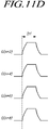
- FIGS. 9 to 11D illustrates four gate signals output from the second gate driving circuit GDC2 when the gate driving circuit 130 illustrated in FIG. 9 is used.
- four first output buffer circuits (GBUF11, GBUF12, GBUF13, and GBUF14) included in the first gate driving circuit GDC1 may include a first output buffer circuit GBUF11 capable of receiving an (n+1)-th clock signal CLK(n+1) and outputting an (n+1)-th gate signal G(n+1) based on the (n+1)-th clock signal CLK(n+1), a first output buffer circuit GBUF12 capable of receiving an (n+3)-th clock signal CLK(n+3) and outputting an (n+3)-th gate signal G(n+3) based on the (n+3)-th clock signal CLK(n+3), a first output buffer circuit GBUF13 capable of receiving an (n+5)-th clock signal CLK(n+5) and outputting an (n+5)-th gate signal G(n+5) based on the (n+5)-th clock signal CLK(n+5), and
- each of the four first output buffer circuits may include a pull-up transistor Tu1 and a pull-down transistor Td1.
- the pull-up transistor Tu1 and the pull-down transistor Td1 may be connected in series between a node to which a corresponding clock signal is applied and a node to which a base voltage GVSS0 is applied.
- a point where the pull-up transistor Tu1 and the pull-down transistor Td1 are connected is a point to which a corresponding gate line is connected and a corresponding gate signal is output.
- All the gate nodes of the respective pull-up transistor Tu1 included in the four first output buffer circuits may be electrically connected to one first Q node Q1
- all the gate nodes of the respective pull-down transistors Td1 included in the four first output buffer circuits may be electrically connected to one first QB node QB1.
- a first control circuit 510 can receive a start signal VST, a reset signal RST, and the like, and control the operations of the four first output buffer circuits (GBUF11, GBUF12, GBUF13, and GBUF14).
- four second output buffer circuits (GBUF21, GBUF22, GBUF23, and GBUF24) included in the second gate driving circuit GDC2 may include a second output buffer circuit GBUF21 capable of receiving an (n+2)-th clock signal CLK(n+2) and outputting an (n+2)-th gate signal G(n+2) based on the (n+2)-th clock signal CLK(n+2), a second output buffer circuit GBUF22 capable of receiving an (n+4)-th clock signal CLK(n+4) and outputting an (n+4)-th gate signal G(n+4) based on the (n+4)-th clock signal CLK(n+4), a second output buffer circuit GBUF23 capable of receiving an (n+6)-th clock signal CLK(n+6) and outputting an (n+6)-th gate signal G(n+6) based on the (n+6)-th clock signal CLK(n+6),
- each of the four second output buffer circuits may include a pull-up transistor Tu2 and a pull-down transistor Td2.
- the pull-up transistor Tu2 and the pull-down transistor Td2 may be connected in series between a node to which a corresponding clock signal is applied and a node to which a base voltage GVSS0 is applied.
- a point where the pull-up transistor Tu2 and the pull-down transistor Td2 are connected is a point to which a corresponding gate line is connected and a corresponding gate signal is output.
- All the gate nodes of the respective pull-up transistor Tu2 included in the second output buffer circuits may be electrically connected to one second Q node Q2, and all the gate nodes of the respective pull-down transistors Td2 included in the four second output buffer circuits (GBUF21, GBUF22, GBUF23, and GBUF24) may be electrically connected to one second QB node QB2.
- a second control circuit 520 can receive a start signal VST, a reset signal RST, and the like, and control the operations of the four second output buffer circuits (GBUF21, GBUF22, GBUF23, and GBUF24).
- the first gate driving circuit GDC1 has the second clock input structure. Accordingly, the respective high level voltage durations of the (n+1)-th clock signal CLK(n+1)), (n+3)-th clock signal (CLK(n+3)), (n+5)-th clock signal (CLK(n+5)), and (n+7)-th clock signal (CLK(n+7)), which are input to the four first output buffer circuits (GBUF11, GBUF12, GBUF13, and GBUF14) included in the first gate driving circuit GDC1, may not overlap one another even when the high level voltage durations have a period of 2H.
- the first Q node Q1 shared by the four first output buffer circuits may not significantly subject to the respective voltage fluctuations (rising and falling) of the four clock signals (CLK(n+1), CLK(n+3), CLK(n+5) and CLK(n+7)).
- a voltage of the first Q node Q1 can rise as the first clock signal CLK(n+1) of the four clock signals (CLK(n+1), CLK(n+3), CLK(n+5), CLK(n+7)) rises, and the voltage of the first Q node Q1 can fall as the last clock signal CLK(n+7) of the four clock signals (CLK(n+1), CLK(n+3), CLK(n+5), CLK(n+7)) falls.
- the first Q node Q1 During a period between a rising time of the first clock signal CLK(n+1) and a falling time of the last clock signal CLK(n+7), the first Q node Q1 remains at a constant voltage, and thus, a large voltage fluctuation such as a step-like voltage fluctuation is not produced.
- the respective rising characteristics (rising periods) and falling characteristics (falling periods) of four gate signals (G(n+1), G(n+3), G(n+5), G(n+7)) output from the four first output buffer circuits (GBUF11, GBUF12, GBUF13, and GBUF14) included in the first gate driving circuit GDC1 may be substantially, or nearly, equal, or similar to one another. That is, although the first gate driving circuit GDC1 performs the overlapping gate driving and has the Q node sharing structure, the second clock input structure applied to the first gate driving circuit GDC1 enables output characteristic differences (a rising characteristic difference and a falling characteristic difference) of gate signals to be reduced.
- the second gate driving circuit GDC2 has the second clock input structure. Accordingly, the respective high level voltage durations of the (n+2)-th clock signal CLK(n+2)), (n+4)-th clock signal (CLK(n+4)), (n+6)-th clock signal (CLK(n+6)), and (n+8)-th clock signal (CLK(n+8)), which are input to the four second output buffer circuits (GBUF21, GBUF22, GBUF23, and GBUF24) included in the second gate driving circuit GDC2, may not overlap one another even when the high level voltage durations have a period of 2H.
- the second Q node Q2 shared by the four first output buffer circuits may not significantly subject to the respective voltage fluctuations of the four clock signals (CLK(n+2), CLK(n+4), CLK(n+6) and CLK(n+8)).
- the respective rising characteristics (rising periods) and falling characteristics (falling periods) of four gate signals (G(n+2), G(n+4), G(n+6), G(n+8)) output from the four second output buffer circuits (GBUF21, GBUF22, GBUF23, and GBUF24) included in the second gate driving circuit GDC2 may be substantially, or nearly, equal, or similar to one another. That is, although the second gate driving circuit GDC2 performs the overlapping gate driving and has the Q node sharing structure, the second clock input structure applied to the second gate driving circuit GDC2 enables output characteristic differences (a rising characteristic difference and a falling characteristic difference) of gate signals to be reduced.
- FIG. 12 illustrates that respective cases (Case 1 and Case 2) in which the gate driving circuit 130 of the display device 100 according to aspects of the present disclosure has the first clock input structure and the second clock input structure.
- the first gate driving circuit GDC1 when the first gate driving circuit GDC1 has the first clock input structure (Case 1), the first gate driving circuit GDC1 can receive four sequential clock signals (CLK(n+1), CLK(n+2), CLK(n+3), and CLK(n+4)).
- the respective high level voltage durations of the four clock signals (CLK(n+1), CLK(n+2), CLK(n+3), and CLK(n+4)) input to the first gate driving circuit GDC1 have a period of 2H.
- the high level voltage duration of the (n+1)-th clock signal CLK(n+1) and the high level voltage duration of the (n+2)-th clock signal CLK(n+2) may partially overlap, the high level voltage duration of the (n+2)-th clock signal CLK(n+2) and the high level voltage duration of the (n+3)-th clock signal CLK(n+3) may partially overlap, and the high level voltage duration of the (n+3)-th clock signal CLK(n+3) and the high level voltage duration of the (n+4)-th clock signal CLK(n+4) may partially overlap.
- the first Q node Q1 in the first gate driving circuit GDC1 may significantly subject to the four clock signals (CLK(n+1), CLK(n+2), CLK(n+3), and CLK(n+4)) whose respective high level voltage durations partially overlap one another. Therefore, this may lead voltage fluctuations to be severely produced, and in turn, lead differences in output characteristics of corresponding gate signals (G(n+1), G(n+2), G(n+3), and G(n+4)) to increase.
- the first gate driving circuit GDC1 when the first gate driving circuit GDC1 has the second clock input structure (Case 2), the first gate driving circuit GDC1 can receive four non-sequential clock signals (CLK(n+1), CLK(n+3), CLK(n+5), and CLK(n+7)).
- the non-sequencing of the clock signals may mean that durations between start times (rising times) of the respective high level voltage durations of the clock signals (e.g., (CLK(n+1), CLK(n+3), CLK(n+5), CLK(n+7)) do not have a period of 1H.
- clock signals e.g., CLK(n+1), CLK(n+2), CLK(n+3), and CLK(n+4) in FIG.
- 6A are defined as being sequential, which may mean that durations between start times (rising times) of the clock signals (e.g., CLK(n+1), CLK(n+2), CLK(n+3), and CLK(n+4)) have a period of 1H.
- start times e.g., CLK(n+1), CLK(n+2), CLK(n+3), and CLK(n+4)
- the respective high level voltage durations of the four clock signals (CLK(n+1), CLK(n+3), CLK(n+5), and CLK(n+7)) input to the first gate driving circuit GDC1 have a period of 2H and do not overlap one another.
- the first Q node Q1 in the first gate driving circuit GDC1 may not significantly subject to the four clock signals (CLK(n+1), CLK(n+3), CLK(n+5), and CLK(n+7)) whose respective high level voltage durations do not overlap one another. Therefore, differences in output characteristics of corresponding gate signals (G(n+1), G(n+3), G(n+5), and G(n+4)) can be reduced.
- FIG. 13 illustrates an example implementation of the gate driving circuit 130 illustrated in FIG. 10 .
- FIG. 13 illustrates a configuration resulting from partially modifying the gate driving circuit 130 of FIG. 10 , and thus, for convenience of description, discussions on equal elements and operations will be omitted.
- the first gate driving circuit GDC1 may further include a first carry output buffer circuit CBUF1 capable of receiving an (n+1)-th carry clock signal CRCLK(n+1) and outputting a carry signal C(n+1), and the second gate driving circuit GDC2 may further include a second carry output buffer circuit CBUF2 capable of receiving an (n+2)-th carry clock signal CRCLK(n+2) and outputting a carry signal C(n+2).
- a first carry output buffer circuit CBUF1 capable of receiving an (n+1)-th carry clock signal CRCLK(n+1) and outputting a carry signal C(n+1)
- the second gate driving circuit GDC2 may further include a second carry output buffer circuit CBUF2 capable of receiving an (n+2)-th carry clock signal CRCLK(n+2) and outputting a carry signal C(n+2).
- the first carry output buffer circuit CBUF1 may include a pull-up transistor Tuc1 and a pull-down transistor Tdc1 that are connected in series between a node to which the (n+1)-th carry clock signal CRCLK(n+1) is input and a node to which a base voltage GVSS2 is applied.
- the second carry output buffer circuit CBUF2 may include a pull-up transistor Tuc2 and a pull-down transistor Tdc2 that are connected in series between a node to which the (n+2)-th carry clock signal CRCLK(n+2) is input and a node to which the base voltage GVSS2 is applied.
- capacitors CAP GS and CAP_CR may be connected between gates node and source nodes (nodes from which a gate signal or a carry signal is output) of the pull-up transistors (Tu1, Tuc1, Tu2, and Tuc2).
- gate signals (G(n+1) to G(n+8)) output from the gate driving circuit 130 of FIGS. 9 and 10 are supplied to gate lines GL(n+1) to GL (n+8)). That is, a structure in which the eight output buffer circuits (GBUF11, GBUF12, GBUF13, GBUF14, GBUF21 GBUF22, GBUF23, and GBUF24) are connected with the eight gate lines (GL(n+1) to GL(n+8)) in FIG. 10 will be described.
- FIG. 14 schematically illustrates the gate driving circuit 130 illustrated in FIG. 10 .
- FIGS. 15 and 16 illustrate connection structures between the gate driving circuit of FIG. 14 and gate lines (GL(n+1) to GL(n+8)) disposed in the display area.
- an (n+1)-th gate signal G(n+1), an (n+3)-th gate signal G(n+3), an (n+5)-th gate signal G(n+5), and an (n+7)-th gate signal G(n+7) may be applied to an (n+1)-th gate line GL(n+1), an (n+3)-th gate line GL(n+3), an (n+5)-th gate line GL(n+5), and an (n+7)-th gate line GL(n+7), respectively.
- an (n+2)-th gate signal G(n+2), an (n+4)-th gate signal G(n+4), an (n+6)-th gate signal G(n+6), and an (n+8)-th gate signal G(n+8) may be applied to an (n+2)-th gate line GL(n+2), an (n+4)-th gate line GL(n+4), an (n+6)-th gate line GL(n+6), and an (n+8)-th gate line GL(n+8), respectively.
- the display panel 110 may include at least one of a connection line CL connecting between the first output buffer circuit GBUF11 outputting the (n+1)-th gate signal G(n+1) and the (n+1)-th gate line GL(n+1) disposed in the display panel 110, a connection line CL connecting between the first output buffer circuit GBUF12 outputting the (n+3)-th gate signal G(n+3) and the (n+3)-th gate line GL(n+3) disposed in the display panel 110, a connection line CL connecting between the first output buffer circuit GBUF13 outputting the (n+5)-th gate signal G(n+5) and the (n+5)-th gate line GL(n+5) disposed in the display panel 110, a connection line CL connecting between the first output buffer circuit GBUF14 outputting the (n+7)-th gate signal G(n+7) and the (n+7)-th gate line GL(n+7) disposed in the display panel 110, a connection line CL connecting between the second output buffer circuit GBUF21 out
- connection structure of FIG. 15 although there is a disadvantage of requiring the separate connection line CL, there is provided an advantage in which data driving can be sequentially performed according to the gate lines (GL(n+1) to GL(n+8)).
- the (n+1)-th gate signal G(n+1), the (n+3)-th gate signal G(n+3), an (n+2)-th gate signal G(n+2), and an (n+4)-th gate signal G(n+4) may be applied to the (n+1)-th gate line GL(n+1), the (n+2)-th gate line GL(n+2), an (n+1+m)-th gate line, and an (n+2+m)-th gate line, respectively.
- the (n+1)-th gate signal G(n+1), the (n+3)-th gate signal G(n+3), the (n+5)-th gate signal G(n+5), the (n+7)-th gate signal G(n+7), the (n+2)-th gate signal G(n+2), the (n+4)-th gate signal G(n+4), the (n+6)-th gate signal G(n+6), and the (n+8)-th gate signal G(n+8) may be applied to the (n+1)-th gate line GL(n+1), the (n+2)-th gate line GL(n+2), the (n+3)-th gate line GL(n+3), the (n+4)-th gate line GL(n+4), the (n+5)-th gate line GL(n+5), the (n+6)-th gate line GL(n+6), the (n+7)-th gate line GL(n+7),
- an order in which the gate signals (G(n+1) to G(n+8)) are output from the gate driving circuit 130 and an order in which the gate lines (GL(n+1) to GL(n) +8)) are arranged are consistent. Accordingly, output portions of the gate driving circuit 130 may be directly connected to the gate lines (GL(n+1) to GL(n+8)) disposed in the display area DA of the display panel 110 without a separate connection line. In consequence, the layout of the display panel 110 may be simplified.
- FIG. 17 illustrates an example of the gate driving circuit 130 illustrated in FIG. 7A .
- various values of m may be used.
- the first gate driving circuit GDC1 may include four first output buffer circuits capable of receiving four clock signals (CLK(n+1), CLK(n+4), CLK(n+7), and CLK(n+10)) included in a first clock signal group CSG1, and outputting four gate signals (G(n+1), G(n+4), G(n+7), and G(n+10)).
- the second gate driving circuit GDC2 may include four second output buffer circuits capable of receiving four clock signals (CLK(n+2), CLK(n+5), CLK(n+8), and CLK(n+11)) included in a second clock signal group CSG2 and outputting four gate signals (G(n+2), G(n+5), G(n+8), and G(n+11)).
- the first gate driving circuit GDC1 has the second clock input structure.
- the respective high level voltage durations of the four clock signals (CLK(n+1), CLK(n+4), CLK(n+7), and CLK(n+10)) input to the first gate driving circuit GDC1 have a period of 2H, the high level voltage durations do not overlap one another.
- the respective rising characteristics (rising periods) and falling characteristics (falling periods) of the four gate signals (G(n+1), G(n+4), G(n+7), and G(n+10)) output from the first gate driving circuit GDC1 may be substantially, or nearly, equal, or similar to one another. That is, although the first gate driving circuit GDC1 performs the overlapping gate driving and has the Q node sharing structure, the second clock input structure applied to the first gate driving circuit GDC1 enables output characteristic differences (a rising characteristic difference and a falling characteristic difference) of gate signals to be reduced.
- the second gate driving circuit GDC2 has the second clock input structure.
- the respective high level voltage durations of the four clock signals (CLK(n+2), CLK(n+5), CLK(n+8), and CLK(n+11)) input to the second gate driving circuit GDC2 have a period of 2H, the high level voltage durations do not overlap one another.
- the respective rising characteristics (rising periods) and falling characteristics (falling periods) of the four gate signals (G(n+2), G(n+5), G(n+8), and G(n+11)) output from the second gate driving circuit GDC2 may be substantially, or nearly, equal, or similar to one another. That is, although the second gate driving circuit GDC2 performs the overlapping gate driving and has the Q node sharing structure, the second clock input structure applied to the second gate driving circuit GDC2 enables output characteristic differences (a rising characteristic difference and a falling characteristic difference) of gate signals to be reduced.
- the gate driving circuit having the clock input structure capable of reducing differences in output characteristics between gate signals, and thereby, improving image quality, and the display device including the gate driving circuit.
- the gate driving circuit having the clock input structure in which overlap gate driving and the Q node sharing structure are enabled while reducing differences in output characteristics between gate signals, and the display device including the gate driving circuit.
Landscapes
- Engineering & Computer Science (AREA)
- Physics & Mathematics (AREA)
- Computer Hardware Design (AREA)
- General Physics & Mathematics (AREA)
- Theoretical Computer Science (AREA)
- Chemical & Material Sciences (AREA)
- Crystallography & Structural Chemistry (AREA)
- Control Of Indicators Other Than Cathode Ray Tubes (AREA)
- Liquid Crystal Display Device Control (AREA)
Abstract
Description
- This application claims the priority benefit Republic of
Korea Patent Application No. 10-2020-0183696, filed on December 24, 2020 - The present disclosure relates to a gate driving circuit and a display device (e.g., a touch display device) including the gate driving circuit.
- As the advent of information society, there have been growing needs for display devices for displaying images. To meet such needs, recently, various types of display devices, such as a Liquid Crystal Display (LCD) device, an Electroluminescence Display (ELD) device including a Quantum-dot Light Emitting Display device, and an Organic Light Emitting Display (e.g., OLED) device, and the like, have been developed and widely used.
- Generally, display devices charge a capacitor disposed in each of a plurality of sub-pixels arranged on a display panel and use the charged capacitance for display driving. However, in such typical display devices, such a capacitor in each sub-pixel may be insufficiently charged, and thereby, image quality may be deteriorated.
- In typical display devices, if a size of the non-display area of a display panel can be reduced, design freedom of the display device can be increased and design quality can be improved. However, since various lines and circuit elements are arranged in the non-display area of the display panel, in actual, it is not easy to reduce the size of the non-display area of the display panel.
- In addition, in the case of such a typical display device, an insufficient charging time may cause image quality to become poor, and further, gate driving may malfunction due to differences in output characteristics between gate signals, this leading image quality to become poor.
- Embodiments of the present disclosure provide a gate driving circuit having a clock input structure capable of reducing differences in output characteristics between gate signals, and thereby, improving image quality, and a display device including the gate driving circuit.
- Embodiments of the present disclosure provide a gate driving circuit having a clock input structure in which overlap gate driving and a Q node sharing structure are enabled while reducing differences in output characteristics between gate signals, and a display device including the gate driving circuit. According an aspect of the present disclosure, a gate driving circuit according to
claim 1 is provided. Further aspects are described in the dependent claims. Aspects and embodiments described herein in connection with the gate driving circuit are analogously applicable to the display device, and vice versa. - According to aspects of the present disclosure, a display device is provided that includes a display panel including a plurality of gate lines, a gate driving circuit including a first gate driving circuit capable of outputting m first gate signals using a first clock signal group, and a second gate driving circuit capable of outputting m second gate signals using a second clock signal group different from the first clock signal group, where m is a natural number of 2 or more.
- Each of the first clock signal group and the second clock signal group may respectively include m first clock signals and m second clock signals, and 2m clock signals including the m first clock signals included in the first clock signal group and the m second clock signals included in the second clock signal group may have respective high level voltage durations at different timings.
- The first gate driving circuit may include m first output buffer circuits receiving the m first clock signals and outputting m first gate signals, and a first control circuit capable of controlling the m first output buffer circuits.
- The second gate driving circuit may include m second output buffer circuits receiving the m second clock signals and outputting m second gate signals, and a second control circuit capable of controlling the m second output buffer circuits.
- Each of the m first output buffer circuits may include a pull-up transistor and a pull-down transistor, and all of corresponding gate nodes of the respective pull-up transistors included in the m first output buffer circuits may be electrically connected to one first Q node.
- Each of the m second output buffer circuits can include a pull-up transistor and a pull-down transistor, and all of corresponding gate nodes of the respective pull-up transistors included in the m second output buffer circuits may be electrically connected to one second Q node.
- The m first clock signals input to the first gate driving circuit may include an (n+1)-th clock signal and an (n+k)-th clock signal, and the m second clock signals input to the second gate driving circuit may include an (n+2)-th clock signal and an (n+k+1)-th clock signal, where n is any integer and k is a
natural number 3 or more. - A high level voltage duration of the (n+1)-th clock signal and a high level voltage duration of the (n+2)-th clock signal may partially overlap. A high level voltage duration of the (n+k)-th clock signal and a high level voltage duration of the (n+k+1)-th clock signal may partially overlap.
- The high level voltage duration of the (n+1)-th clock signal and the high level voltage duration of the (n+k)-th clock signal may not overlap. The high level voltage duration of the (n+2)-th clock signal and the high level voltage duration of the (n+k+1)-th clock signal may not overlap.
- m may be equal to the number of pull-up transistors whose gate nodes are commonly connected to the one first Q node and may be equal to the number of pull-up transistors whose gate nodes are commonly connected to the one second Q node.
- k may be proportional to a length of a high level voltage duration of each of the 2m clock signals and a value obtained by multiplying one horizontal period by (k-1) may be equal to the length of the high level voltage duration of each of the 2m clock signals.
- k may be 3 or 4.
- In the case of k=3, the m first output buffer circuits included in the first gate driving circuit may include one first output buffer circuit receiving the (n+1)-th clock signal and outputting an (n+1)-th gate signal, and another first output buffer circuit receiving an (n+3)-th clock signal and outputting an (n+3)-th gate signal. The m second output buffer circuits included in the second gate driving circuit may include one second output buffer circuit receiving the (n+2)-th clock signal and outputting an (n+2)-th gate signal, and another second output buffer circuit receiving an (n+4)-th clock signal and outputting an (n+4)-th gate signal.
- In the case of k=3, the (n+1)-th gate signal may be applied to an (n+1)-th gate line, the (n+3)-th gate signal may be applied to an (n+3)-th gate line, the (n+2)-th gate signal may be applied to an (n+2)-th gate line, and the (n+4)-th gate signal may be applied to an (n+4)-th gate line.
- In this case, the display device (e.g., the display panel thereof) may include at least one of a connection line connecting between the one first output buffer circuit outputting the (n+1)-th gate signal and the (n+1)-th gate line disposed in the display panel, a connection line connecting between the another first output buffer circuit outputting the (n+3)-th gate signal and the (n+3)-th gate line disposed in the display panel, a connection line between connecting the one second output buffer circuit outputting the (n+2)-th gate signal and the (n+2)-th gate line disposed in the display panel, and a connection line connecting between the another second output buffer circuit outputting the (n+4)-th gate signal and the (n+4)-th gate line disposed in the display panel.
- In the case of k=3, the (n+1)-th gate signal may be applied to the (n+1)-th gate line, the (n+3)-th gate signal may be applied to the (n+2)-th gate line, the (n+2)-th gate signal may be applied to an (n+1+m)-th gate line, and the (n+4)-th gate signal may be applied to an (n+2+m)-th gate line.
- In the case of k=3 and m=4, the m first output buffer circuits included in the first gate driving circuit may further include further another first output buffer circuit receiving an (n+5)-th clock signal and outputting an (n+5)-th gate signal, and yet another first output buffer circuit receiving an (n+7)-th clock signal and outputting an (n+7)-th gate signal. The m second output buffer circuits included in the second gate driving circuit may further include further another second output buffer circuit receiving an (n+6)-th clock signal and outputting an (n+6)-th gate signal, and yet another second output buffer circuit receiving an (n+8)-th clock signal and outputting an (n+8)-th gate signal.
- In the case of k=3 and m=4, the (n+1)-th gate signal may be applied to the (n+1)-th gate line, the (n+3)-th gate signal may be applied to the (n+3)-th gate line, the (n+5)-th gate signal may be applied to an (n+5)-th gate line, the (n+7)-th gate signal may be applied to an (n+7)-th gate line, the (n+2)-th gate signal may be applied to the (n+2)-th gate line, the (n+4)-th gate signal may be applied to the (n+4)-th gate line, and the (n+6)-th gate signal may be applied to an (n+6)-th gate line, and the (n+8)-th gate signal may be applied to an (n+8)-th gate line.
- In this case, the display device (e.g., the display panel thereof) may include at least one of the connection line connecting between the one first output buffer circuit outputting the (n+1)-th gate signal and the (n+1)-th gate line disposed in the display panel, the connection line connecting between the another first output buffer circuit outputting the (n+3)-th gate signal and the (n+3)-th gate line disposed in the display panel, a connection line connecting between the further another first output buffer circuit outputting the (n+5)-th gate signal and the (n+5)-th gate line disposed in the display panel, a connection line connecting between the yet another first output buffer circuit outputting the (n+7)-th gate signal and the (n+7)-th gate line disposed in the display panel, the connection line connecting between the one second output buffer circuit outputting the (n+2)-th gate signal and the (n+2)-th gate line disposed in the display panel, the connection line connecting between the another second output buffer circuit outputting the (n+4)-th gate signal and the (n+4)-th gate line disposed in the display panel, a connection line connecting between the further another second output buffer circuit outputting the (n+6)-th gate signal and the (n+6)-th gate line disposed in the display panel, and a connection line connecting between the yet another second output buffer circuit outputting the (n+8)-th gate signal and the (n+8)-th gate line disposed in the display panel.
- In the case of k=3 and m=4, the (n+1)-th gate signal may be applied to the (n+1)-th gate line, the (n+3)-th gate signal may be applied to the (n+2)-th gate line, the (n+5)-th gate signal may be applied to the (n+3)-th gate line, the (n+7)-th gate signal may be applied to the (n+4)-th gate line, the (n+2)-th gate signal may be applied to the (n+1+m)-th gate line, the (n+4)-th gate signal may be applied to the (n+2+m)-th gate line, the (n+6)-th gate signal may be applied to an (n+3+m)-th gate line, and the (n+8)-th gate signal may be applied to an (n+4+m)-th gate line.
- The first gate driving circuit can output the (n+1)-th gate signal based on the (n+1)-th clock signal and an (n+k)-th gate signal based on an (n+k)-th clock signal. The second gate driving circuit can output the (n+2)-th gate signal based on the (n+2)-th clock signal and an (n+k+1)-th gate signal based on an (n+k+1)-th clock signal.
- A turn-on level voltage duration of the (n+1)-th gate signal may partially overlap a turn-on level voltage duration of the (n+2)-th gate signal, and the turn-on level voltage duration of the (n+1)-th gate signal may not overlap a turn-on level voltage duration of the (n+k)-th gate signal.
- The display panel may include a display area and a non-display area different from the display area. The gate driving circuit may be disposed in the non-display area.
- According to aspects of the present disclosure, a gate driving circuit capable of driving a plurality of gate lines disposed in a display panel is provided. The gate driving circuit has the same structure as that included in the above display device.
- According to embodiments of the present disclosure, it is possible to provide the gate driving circuit having a clock input structure capable of reducing differences in output characteristics between gate signals, and thereby, improving image quality, and the display device including the gate driving circuit.
- According to embodiments of the present disclosure, it is possible to provide the gate driving circuit having a clock input structure in which overlap gate driving and a Q node sharing structure are enabled while reducing differences in output characteristics between gate signals, and the display device including the gate driving circuit.
- The accompanying drawings, which are included to provide a further understanding of the disclosure and are incorporated in and constitute a part of the disclosure, illustrate aspects of the disclosure and together with the description serve to explain the principle of the disclosure. In the drawings:
-
FIG. 1 illustrates a system configuration of a display device according to aspects of the present disclosure; -
FIGS. 2A and2B illustrate equivalent circuits for a sub-pixel of the display device according to aspects of the present disclosure; -
FIG. 3 illustrates an example system implementation of the display device according to aspects of the present disclosure; -
FIG. 4 is a block diagram of a gate driving circuit of the display device according to aspects of the present disclosure; -
FIG. 5 illustrates a gate driving circuit having a first clock input structure included in the display device according to aspects of the present disclosure; -
FIG. 6A illustrates 4 clock signals input to a first gate driving circuit when the gate driving circuit illustrated inFIG. 5 is used, and voltage fluctuations at a Q node of the first gate driving circuit; -
FIG. 6B illustrates 4 gate signals output from the first gate driving circuit when the gate driving circuit illustrated inFIG. 5 is used; -
FIG. 7A illustrates a gate driving circuit having a second clock input structure included in the display device according to aspects of the present disclosure; -
FIG. 7B illustrates clock signals input to the gate driving circuit illustrated inFIG. 7A ; -
FIG. 8 illustrates the gate driving circuit illustrated inFIG. 7A in more detail; -
FIG. 9 illustrates an example of the gate driving circuit illustrated inFIG. 7A ; -
FIG. 10 illustrates the gate driving circuit illustrated inFIG. 9 in more detail; -
FIG. 11A illustrates 4 clock signals input to a first gate driving circuit when the gate driving circuit illustrated inFIG. 9 is used, and voltage fluctuations at a Q1 node of the first gate driving circuit; -
FIG. 11B illustrates 4 gate signals output from the first gate driving circuit when the gate driving circuit illustrated inFIG. 9 is used; -
FIG. 11C illustrates 4 clock signals input to a second gate driving circuit when the gate driving circuit illustrated inFIG. 9 is used, and voltage fluctuations at a Q2 node of the second gate driving circuit; -
FIG. 11D illustrates 4 gate signals output from the second gate driving circuit when the gate driving circuit illustrated inFIG. 9 is used; -
FIG. 12 illustrates a result from a simulation for detecting output characteristics for each of the first clock input structure and the second clock input structure used in the gate driving circuit of the display device according to aspects of the present disclosure; -
FIG. 13 illustrates an example implementation of the gate driving circuit illustrated inFIG. 10 ; -
FIG. 14 schematically illustrates the gate driving circuit illustrated inFIG. 10 ; -
FIGS. 15 and16 illustrate connection structures between the gate driving circuit ofFIG. 14 and gate lines disposed in the display area; and -
FIG. 17 illustrates an example of the gate driving circuit illustrated inFIG. 7A . - In the following description of examples or embodiments of the present disclosure, reference will be made to the accompanying drawings in which it is shown by way of illustration specific examples or embodiments that can be implemented, and in which the same reference numerals and signs can be used to designate the same or like components even when they are shown in different accompanying drawings from one another. Further, in the following description of examples or embodiments of the present disclosure, detailed descriptions of well-known functions and components incorporated herein will be omitted when it is determined that the description may make the subject matter in some embodiments of the present disclosure rather unclear. The terms such as "including", "having", "containing", "constituting" "make up of', and "formed of' used herein are generally intended to allow other components to be added unless the terms are used with the term "only". As used herein, singular forms are intended to include plural forms unless the context clearly indicates otherwise.
- Terms, such as "first", "second", "A", "B", "(A)", or "(B)" may be used herein to describe elements of the present disclosure. Each of these terms is not used to define essence, order, sequence, or number of elements etc., but is used merely to distinguish the corresponding element from other elements.
- When it is mentioned that a first element "is connected or coupled to", "contacts or overlaps" etc. a second element, it should be interpreted that, not only can the first element "be directly connected or coupled to" or "directly contact or overlap" the second element, but a third element can also be "interposed" between the first and second elements, or the first and second elements can "be connected or coupled to", "contact or overlap", etc. each other via a fourth element. Here, the second element may be included in at least one of two or more elements that "are connected or coupled to", "contact or overlap", etc. each other.
- When time relative terms, such as "after," "subsequent to," "next," "before," and the like, are used to describe processes or operations of elements or configurations, or flows or steps in operating, processing, manufacturing methods, these terms may be used to describe nonconsecutive or non-sequential processes or operations unless the term "directly" or "immediately" is used together.
- In addition, when any dimensions, relative sizes etc. are mentioned, it should be considered that numerical values for an elements or features, or corresponding information (e.g., level, range, etc.) include a tolerance or error range that may be caused by various factors (e.g., process factors, internal or external impact, noise, etc.) even when a relevant description is not specified. Further, the term "may" fully encompasses all the meanings of the term "can".
-
FIG. 1 illustrates a system configuration of adisplay device 100 according to aspects of the present disclosure. - Referring to
FIG. 1 , thedisplay device 100 according to aspects of the present disclosure includes adisplay panel 110 and a driving circuit for driving thedisplay panel 110. - The driving circuits may include a
data driving circuit 120, agate driving circuit 130, and the like, and may further include acontroller 140 that controls thedata driving circuit 120 and thegate driving circuit 130. - The
display panel 110 may include a substrate SUB, and signal lines such as a plurality of data lines DL, a plurality of gate lines GL, and the like disposed over the substrate SUB. Thedisplay panel 110 may include a plurality of sub-pixels SP connected to the plurality of gate lines GL and the plurality of data lines DL. - The
display panel 110 may include a display area DA in which an image is displayed, and a non-display area NDA, in which an image is not displayed, different from the display area DA. In thedisplay panel 110, the plurality of sub-pixels SP for displaying an image may be disposed in the display area DA, and the drivingcircuits display panel 110. - The
data driving circuit 120 is a circuit for driving the plurality of data lines DL, and can supply data signals to the plurality of data lines DL. Thegate driving circuit 130 is a circuit for driving the plurality of gate lines GL, and can supply gate signals to the plurality of gate lines GL. Thecontroller 140 can supply a data control signal DCS to thedata driving circuit 120 in order to control an operation timing of thedata driving circuit 120. Thecontroller 140 can supply a gate control signal GCS to thegate driving circuit 130 in order to control an operation timing of thegate driving circuit 130. - The
controller 140 starts a scanning operation according to timings scheduled in each frame, converts image data inputted from other devices or other image providing sources (e.g. host systems) to a data signal form used in thedata driving circuit 120 and then supplies image data Data resulting from the converting to thedata driving circuit 120, and controls the loading of the data to at least one pixel at a pre-configured time according to a scan timing. - The
controller 140 can receive, in addition to input image data, several types of timing signals including a vertical synchronous signal VSYNC, a horizontal synchronous signal HSYNC, an input data enable signal DE, a clock signal CLK, and the like from other devices, networks, or systems (e.g. a host system 150). - To control the
data driving circuit 120 and thegate driving circuit 130, thecontroller 140 can receive one or more of the timing signals such as the vertical synchronization signal VSYNC, the horizontal synchronization signal HSYNC, the input data enable signal DE, the clock signal, and the like, generate several types of control signals (DCS, GCS), and supply the generated signals to thedata driving circuit 120 and thegate driving circuit 130. - The
controller 140 may be implemented in a separate component from thedata driving circuit 120, or integrated with thedata driving circuit 120 and implemented into an integrated circuit. - The
data driving circuit 120 can drive a plurality of data lines DL by receiving image data Data from thecontroller 140 and supplying data voltages to the plurality of data lines DL. Here, thedata driving circuit 120 may also be referred to as a source driving circuit. - The
data driving circuit 120 may include one or more source driver integrated circuits SDIC. Each source driver integrated circuit SDIC may include a shift register, a latch circuit, a digital-to-analog converter DAC, an output buffer, and the like. In some instances, each source driver integrated circuit SDIC may further include an analog to digital converter ADC. - In some embodiments, each source driver integrated circuit SDIC may be connected to the
display panel 110 in a tape automated bonding (TAB) type, or connected to a conductive pad such as a bonding pad of thedisplay panel 110 in a chip on glass (COG) type or a chip on panel (COP) type, or connected to thedisplay panel 110 in a chip on film (COF) type. - The
gate driving circuit 130 can output a gate signal of a turn-on level voltage or a gate signal of a turn-off level voltage according to the control of thecontroller 140. Thegate driving circuit 130 can sequentially drive a plurality of gate lines GL by sequentially supplying the gate signal of the turn-on level voltage to the plurality of gate lines GL. - In some embodiments, the
gate driving circuit 130 may be connected to thedisplay panel 110 in the tape automated bonding (TAB) type, or connected to a conductive pad such as a bonding pad of thedisplay panel 110 in the chip on glass (COG) type or the chip on panel (COP) type, or connected to thedisplay panel 110 in the chip on film (COF) type. In another embodiment, thegate driving circuit 130 may be located in the non-display area NDA of thedisplay panel 110 in a gate in panel (GIP) type. Thegate driving circuit 130 may be disposed on or over a substrate SUB, or connected to the substrate SUB. That is, in the case of the GIP type, thegate driving circuit 130 may be disposed in the non-display area NDA of the substrate SUB. Thegate driving circuit 130 may be connected to the substrate SUB in the case of the chip on glass (COG) type, the chip on film (COF) type, or the like. - At least one of the
data driving circuit 120 and thegate driving circuit 130 may be disposed in the display area DA. For example, at least one of thedata driving circuit 120 and thegate driving circuit 130 may be disposed not to overlap sub-pixels SP, or disposed to overlap one or more, or all, of the sub-pixels SP. - When a specific gate line is asserted by the
gate driving circuit 130, thedata driving circuit 120 can convert image data Data received from thecontroller 140 into data voltages in an analog form and supplies the data voltages resulting from the converting to a plurality of data lines DL. - The
data driving circuit 120 may be located on, but not limited to, only one portion (e.g., an upper portion or a lower portion) of thedisplay panel 110. In some embodiments, thedata driving circuit 120 may be located on, but not limited to, two portions (e.g., an upper portion and a lower portion) of thedisplay panel 110 or at least two of four portions (e.g., the upper portion, the lower portion, a left side, and a right side) of thedisplay panel 110 according to driving schemes, panel design schemes, or the like. - The
gate driving circuit 130 may be located on, but not limited to, only one portion (e.g., a left side or a right side) of thedisplay panel 110. In some embodiments, thegate driving circuit 130 may be located on, but not limited to, two portions (e.g., a left side and a right side) of thedisplay panel 110 or at least two of four portions (e.g., an upper portion, a lower portion, the left side, and the right side) of thedisplay panel 110 according to driving schemes, panel design schemes, or the like. - The
controller 140 may be a timing controller used in the typical display technology or a control apparatus/device capable of additionally performing other control functionalities in addition to the typical function of the timing controller. In some embodiments, thecontroller 140 may be one or more other control circuits different from the timing controller, or a circuit or component in the control apparatus/device Thecontroller 140 may be implemented using various circuits or electronic components such as an integrated circuit (IC), a field programmable gate array (FPGA), an application specific integrated circuit (ASIC), a processor, and/or the like. - The
controller 140 may be mounted on a printed circuit board, a flexible printed circuit, or the like, and may be electrically connected to thedata driving circuit 120 and thegate driving circuit 130 through the printed circuit board, the flexible printed circuit, or the like. - The
controller 140 may transmit signals to, and receive signals from, thedata driving circuit 120 via one or more predetermined interfaces. In some embodiments, such interfaces may include a low voltage differential signaling (LVDS) interface, an EPI interface, a serial peripheral interface (SPI), and the like. Thecontroller 140 may include a storage medium such as one or more registers. - The
display device 100 according to aspects of the present disclosure may be a display including a backlight unit such as a liquid crystal display device, or may be a self-emissive display such as an organic light emitting diode (OLED) display, a quantum dot (QD) display, a micro light emitting diode (M-LED) display, and the like. - In case the
display device 100 according to aspects of the present disclosure is the OLED display, each sub-pixel SP may include an OLED where the OLED itself emits light as a light emitting element. In case thedisplay device 100 according to aspects of the present disclosure is the QD display, each sub-pixel SP may include a light emitting element including a quantum dot, which is a self-emissive semiconductor crystal. In case thedisplay device 100 according to aspects of the present disclosure is the micro LED display, each sub-pixel SP may include a micro LED where the micro OLED itself emits light and which is based on an inorganic material as a light emitting element. -
FIGS. 2A and2B illustrate example equivalent circuits for a sub-pixel SP of thedisplay device 100 according to aspects of the present disclosure. - Referring to
FIG. 2A , each of a plurality of sub-pixels SP disposed in thedisplay panel 110 of thedisplay device 100 according to aspects of the present disclosure may include a light emitting element ED, a driving transistor DRT, and a scan transistor SCT and a storage capacitor Cst. - Referring to
FIG. 2A , the light emitting element ED may include a pixel electrode PE and a common electrode CE, and include an emission layer EL located between the pixel electrode PE and the common electrode CE. - The pixel electrode PE of the light emitting element ED may be an electrode disposed in each sub-pixel SP, and the common electrode CE may be an electrode commonly disposed in all or some of the sub-pixels SP. Here, the pixel electrode PE may be an anode electrode and the common electrode CE may be a cathode electrode. In another embodiment, the pixel electrode PE may be the cathode electrode and the common electrode CE may be the anode electrode.
- In one embodiment, the light emitting element ED may be an organic light emitting diode (OLED), a light emitting diode (LED), a quantum dot light emitting element or the like.
- The driving transistor DRT may be a transistor for driving the light emitting element ED, and may include a first node N1, a second node N2, a third node N3, and the like.
- The first node N1 of the driving transistor DRT may be a gate node of the driving transistor DRT, and may be electrically connected to a source node or a drain node of the scan transistor SCT. The second node N2 of the driving transistor DRT may be a source node or a drain node of the driving transistor DRT. The second node N2 may be also electrically connected to a source node or a drain node of a sensing transistor SENT, and connected to the pixel electrode PE of the light emitting element ED. A third node N3 of the driving transistor DRT may be electrically connected to a driving voltage line DVL for supplying a driving voltage EVDD.
- The scan transistor SCT can be controlled by a scan signal SCAN, which is a type of gate signal, and may be connected between the first node N1 of the driving transistor DRT and a data line DL. In other words, the scan transistor SCT can be turned on or off according to the scan signal SCAN supplied through a scan signal line SCL, which is a type of the gate line GL, and control an electrical connection between the data line DL and the first node N1 of the driving transistor DRT.
- The scan transistor SCT can be turned on by a scan signal SCAN having a turn-on level voltage, and passes a data voltage Vdata supplied through the data line DL to the first node of the driving transistor DRT.
- In one embodiment, when the scan transistor SCT is an n-type transistor, the turn-on level voltage of the scan signal SCAN may be a high level voltage. In another embodiment, when the scan transistor SCT is a p-type transistor, the turn-on level voltage of the scan signal SCAN may be a low level voltage.
- The storage capacitor Cst may be connected between the first node N1 and the second node N2 of the driving transistor DRT. The storage capacitor Cst can store the amount of electric charge corresponding to a voltage difference between both terminals and maintain the voltage difference between both terminals for a predetermined frame time. Accordingly, a corresponding sub-pixel SP can emit light for the predetermined frame time.
- Referring to
FIG. 2B , each of the plurality of sub-pixels SP disposed in thedisplay panel 110 of thedisplay device 100 according to aspects of the present disclosure may further include a sensing transistor SENT. - The sensing transistor SENT can be controlled by a sense signal SENSE, which is another type of gate signal, and may be connected between the second node N2 of the driving transistor DRT and a reference voltage line RVL. In other words, the sensing transistor SENT can be turned on or off according to the sense signal SENSE supplied through a sense signal line SENL, which is another type of the gate line GL, and control an electrical connection between the reference voltage line RVL and the second node N2 of the driving transistor DRT.
- The sensing transistor SENT can be turned on by a sense signal SENSE having a turn-on level voltage, and pass a reference voltage Vref transmitted through the reference voltage line RVL to the second node of the driving transistor DRT.
- Further, the sensing transistor SENT can be turned on by the sense signal SENSE having the turn-on level voltage, and transmit a voltage at the second node N2 of the driving transistor DRT to the reference voltage line RVL.
- In one embodiment, when the sensing transistor SENT is an n-type transistor, the turn-on level voltage of the sense signal SENSE may be a high level voltage. In another embodiment, when the sensing transistor SENT is a p-type transistor, the turn-on level voltage of the sense signal SENSE may be a low level voltage.
- The function of the sensing transistor SENT transmitting the voltage at the second node N2 of the driving transistor DRT to the reference voltage line RVL may be used when driven to sense at least one characteristic value of the sub-pixel SP. In this case, the voltage transmitted to the reference voltage line RVL may be a voltage for calculating at least one characteristic value of the sub-pixel SP or a voltage in which the at least one characteristic value of the sub-pixel SP is reflected.
- Herein, the characteristic value of the sub-pixel SP may be a characteristic value of the driving transistor DRT or the light emitting element ED. The at least one characteristic value of the driving transistor DRT may include a threshold voltage and/or mobility of the driving transistor DRT. The characteristic value of the light emitting element ED may include a threshold voltage of the light emitting element ED.
- The driving transistor DRT, the scan transistor SCT, and the sensing transistor SENT may be n-type transistors, p-type transistors, or combinations thereof. Herein, for convenience of description, it is assumed that the driving transistor DRT, the scan transistor SCT, and the sensing transistor SENT are n-type transistors.
- The storage capacitor Cst may be an external capacitor intentionally designed to be located outside of the driving transistor DRT, other than an internal capacitor, such as a parasitic capacitor (e.g., a Cgs, a Cgd), that may be formed between the gate node and the source node (or drain node) of the driving transistor DRT.
- The scan signal line SCL and the sense signal line SENL may be different gate lines GL. In some embodiments, the scan signal SCAN and the sense signal SENSE may be separate gate signals, and the on-off timing of the scan transistor SCT and the on-off timing of the sensing transistor SENT in one sub-pixel SP may be independent. That is, the on-off timing of the scan transistor SCT and the on-off timing of the sensing transistor SENT in one sub-pixel SP may be equal to, or different from, each other.
- In another embodiment, the scan signal line SCL and the sense signal line SENL may be the same gate line GL. That is, a gate node of the scan transistor SCT and a gate node of the sensing transistor SENT in one sub-pixel SP may be connected to one gate line GL. In this embodiment, the scan signal SCAN and the sense signal SENSE may be the same gate signal, and the on-off timing of the scan transistor SCT and the on-off timing of the sensing transistor SENT in one sub-pixel SP may be the same.
- It should be understood that the sub-pixel structures shown in
FIGS. 2A and2B are merely examples of possible sub-pixel structures for convenience of discussion, and embodiments of the present disclosure may be implemented in any of various structures, as desired. For example, the sub-pixel SP may further include at least one transistor and/or at least one capacitor. - Further, although discussions on the sub-pixel structures in
FIGS. 2A and2B have been conducted based on the assumption that thedisplay device 100 is a self-emissive display device, when thedisplay device 100 is a liquid crystal display, each sub-pixel SP may include a transistor, a pixel electrode, and the like. -
FIG. 3 illustrates an example system implementation of thedisplay device 100 according to aspects of the present disclosure. - Referring to
FIG. 3 , thedisplay panel 110 may include a display area DA in which an image is displayed and a non-display area NDA in which an image is not displayed. - Referring to
FIG. 3 , when thedata driving circuit 120 includes one or more source driver integrated circuits SDIC and is implemented in the chip on film (COF) type, each source driver integrated circuit SDIC may be mounted on a circuit film SF connected to the non-display area NDA of thedisplay panel 110. - Referring to
FIG. 3 , thegate driving circuit 130 may be implemented in the gate in panel (GIP) type. In this embodiment, thegate driving circuit 130 may be located in the non-display area NDA of thedisplay panel 110. In another embodiment, unlike the illustration inFIG. 3 , thegate driving circuit 130 may be implemented in the chip on film (COF) type. - The
display device 100 may include at least one source printed circuit board SPCB for a circuital connection between one or more source driver integrated circuits SDIC and other devices, components, and the like, and a control printed circuit board CPCB on which control components, and various types of electrical devices or components are mounted. - The circuit film SF on which the source driver integrated circuit SDIC is mounted may be connected to at least one source printed circuit board SPCB. That is, one side of the circuit film SF on which the source driver integrated circuit SDIC is mounted may be electrically connected to the
display panel 110 and the other side thereof may be electrically connected to the source printed circuit board SPCB. - The
controller 140 and the power management integrated circuit PMIC, 310 may be mounted on the control printed circuit board CPCB. Thecontroller 140 can perform an overall control function related to the driving of thedisplay panel 110 and control operations of thedata driving circuit 120 and thegate driving circuit 130. The power management integratedcircuit 310 can supply various types of voltages or currents to thedata driving circuit 120 and thegate driving circuit 130 or control various types of voltages or currents to be supplied. - A circuital connection between at least one source printed circuit board SPCB and the control printed circuit board CPCB may be performed through at least one connection cable CBL. The connection cable CBL may be, for example, a flexible printed circuit FPC, a flexible flat cable FFC, or the like.
- At least one source printed circuit board SPCB and the control printed circuit board CPCB may be integrated and implemented into one printed circuit board.
- The
display device 100 according to aspects of the present disclosure may further include alevel shifter 300 for adjusting a voltage level. In one embodiment, thelevel shifter 300 may be disposed on the control printed circuit board CPCB or the source printed circuit board SPCB. - In the
display device 100 according to aspects of the present disclosure, thelevel shifter 300 can supply signals required for gate driving to thegate driving circuit 130. In one embodiment, thelevel shifter 300 can supply a plurality of clock signals to thegate driving circuit 130. Accordingly, thegate driving circuit 130 can supply a plurality of gate signals to a plurality of gate lines GL based on the plurality of clock signals input from thelevel shifter 300. The plurality of gate lines GL can carry the gate signals to the sub-pixels SP disposed in the display area DA of the substrate SUB. -
FIG. 4 is a block diagram of thegate driving circuit 130 of thedisplay device 100 according to aspects of the present disclosure. - Referring to
FIG. 4 , thegate driving circuit 130 included in thedisplay device 100 according to aspects of the present disclosure may be a circuit capable of driving a plurality of gate lines GL disposed on thedisplay panel 110, generating a plurality of gate signals using a plurality of clock signals, and supplying the generated gate signals to the plurality of gate lines GL. - The
gate driving circuit 130 may include a first gate driving circuit GDC1 outputting m gate signals using a first clock signal group CSG1, and a second gate driving circuit GDC2 outputting m gate signals using a second clock signal group CSG2 different from the first clock signal group CSG1, where m is a natural number of 2 or more. - Each of the first clock signal group CSG1 and the second clock signal group CSG2 may include m clock signals, where m is a natural number of 2 or more.
- The first gate driving circuit GDC1 and the second gate driving circuit GDC2 may be circuits that generate and output the scan signals SCAN in the sub-pixel structures of
FIGS. 2A and2B . Accordingly, the m gate signals output from each of the first gate driving circuit GDC1 and the second gate driving circuit GDC2 may be scan signals SCAN. - In another embodiment, the first gate driving circuit GDC1 and the second gate driving circuit GDC2 may be circuits that generate and output the sense signal SENSE in the sub-pixel structure of
FIG. 2B . Accordingly, the m gate signals output from each of the first gate driving circuit GDC1 and the second gate driving circuit GDC2 may be sense signals SENSE. - The first gate driving circuit GDC1 may include m first output buffer circuits. The m first output buffer circuits may be electrically connected to correspond to m gate lines GL. The m first output buffer circuits may output m gate signals to the m gate lines GL. Each of the m first output buffer circuits may include a pull-up transistor and a pull-down transistor.
- The second gate driving circuit GDC2 may include m second output buffer circuits. The m second output buffer circuits may be electrically connected to correspond to m gate lines GL. The m second output buffer circuits may output m gate signals to the m gate lines GL. Each of the m second output buffer circuits may include a pull-up transistor and a pull-down transistor.
- In some embodiments, the
gate driving circuit 130 may have a Q node sharing structure in which one Q node is shared on m output buffer circuits basis, and a QB node sharing structure in which one QB node is shared on m output buffer circuits basis. A size of a bezel area (non-display area NDA) of thedisplay panel 110 can be reduced through the Q node sharing structure and/or the QB node sharing structure. Here, m represents the number of output buffer circuits sharing one Q node, and may represent a basis on which one Q node is shared by output buffer circuits or a size in which one Q node is shared by output buffer circuits. - The first gate driving circuit GDC1 may have one first Q node and one first QB node. The gate nodes of the respective pull-up transistors included in the m first output buffer circuits included in the first gate driving circuit GDC1 can share one first Q node. The gate nodes of the respective pull-down transistors included in the m first output buffer circuits included in the first gate driving circuit GDC1 can share one first QB node.
- The second gate driving circuit GDC2 may include m second output buffer circuits. The m second output buffer circuits may be electrically connected to correspond to m gate lines GL. The m second output buffer circuits may output m gate signals to the m gate lines GL. Each of the m second output buffer circuits may include a pull-up transistor and a pull-down transistor.
- The second gate driving circuit GDC2 may have one second Q node and one second QB node. The gate nodes of the respective pull-up transistors included in the m second output buffer circuits included in the second gate driving circuit GDC2 can share one second Q node. The gate nodes of the respective pull-down transistors included in the m second output buffer circuits included in the second gate driving circuit GDC2 can share one second QB node.
- Further, in some embodiments, the
gate driving circuit 130 can perform overlap gate driving in order to improve image quality by increasing an insufficient charging time in each sub-pixel. - When the
gate driving circuit 130 performs the overlap gate driving, thegate driving circuit 130 can output gate signals having a turn-on level voltage duration longer than a period of one horizontal (1H). In addition, a turn-on level voltage duration of one of the gate signals output from thegate driving circuit 130 may partially overlap a turn-on level voltage duration of another gate signal. - For example, in some embodiments, when the
gate driving circuit 130 performs 2H overlap gate driving, a turn-on level voltage duration of each gate signal may have a time period of 2H. In addition, the period of 1H corresponding to the second half of the turn-on level voltage duration of one gate signal may overlap the period of 1H corresponding to the first half of the turn-on level voltage duration of another gate signal. - In some embodiments, when the
gate driving circuit 130 performs 3H overlap gate driving, a turn-on level voltage duration of each gate signal may have a time period of 3H. In addition, the period of 2H corresponding to the second half of the turn-on level voltage duration of one gate signal may overlap the period of 2H corresponding to the first half of the turn-on level voltage duration of another gate signal. Hereinafter, the Q node sharing structure and overlap gate driving briefly described above will be described again with reference toFIGS. 5 ,6A , and6B . -
FIG. 5 illustrates agate driving circuit 130 having a first clock input structure included in thedisplay device 100 according to aspects of the present disclosure.FIG. 5 illustrates an example in the case of m=4.FIG. 6A illustrates four clock signals (CLK(n+1), CLK(n+2), CLK(n+3), and CLK(n+4)) input to the first gate driving circuit GDC1 and voltage fluctuations at the Q node of the first gate driving circuit GDC1 when thegate driving circuit 130 ofFIG. 5 is used.FIG. 6B illustrates four gate signals (G(n+1), G(n+2), G(n+3), and G(n+4)) output from the first gate driving circuit GDC1 when thegate driving circuit 130 ofFIG. 5 is used. - Referring to
FIG. 5 , the first gate driving circuit GDC1 can output four (m=4) gate signals (G(n+1), G(n+2), G(n+3), and G(n+4)) using four (m=4) clock signals (CLK(n+1), CLK(n+2), CLK(n+3), and CLK(n+4)) included in the first clock signal group CSG1. The second gate driving circuit GDC2 can output four (m=4) gate signals (G(n+5), G(n+6), G(n+7), and G(n+8)) using four (m=4) clock signals (CLK(n+5), CLK(n+6), CLK(n+7), and CLK(n+8)) included in the second clock signal group CSG2. - The first gate driving circuit GDC1 may include four (m=4) first output buffer circuits. The four first output buffer circuits may be electrically connected to correspond to four (m=4) gate lines GL. The four first output buffer circuits can output four (m=4) gate signals (G(n+1), G(n+2), G(n+3), and G(n+4)) to the four gate lines GL. Each of the four first output buffer circuits may include a pull-up transistor and a pull-down transistor.
- The second gate driving circuit GDC2 may include four second output buffer circuits. The four second output buffer circuits may be electrically connected to correspond to four gate lines GL. The four second output buffer circuits can output four gate signals (G(n+5), G(n+6), G(n+7), and G(n+8)) to the four gate lines GL. Each of the four second output buffer circuits may include a pull-up transistor and a pull-down transistor.
- Referring to
FIGS. 5 and6A , the four first output buffer circuits included in the first gate driving circuit GDC1 can share one Q node and one QB node. - The gate nodes of the respective pull-up transistors included in the four first output buffer circuits included in the first gate driving circuit GDC1 can share the one Q node. The gate nodes of the respective pull-down transistors included in the four first output buffer circuits included in the first gate driving circuit GDC1 can share the one QB node.
- Referring to
FIGS. 5 ,6A , and6B , for example, when the first gate driving circuit GDC1 performs 2H overlap gate driving, the first gate driving circuit GDC1 can receive four clock signals CLK(n+1), CLK(n+2), CLK(n+3), and CLK(n+4)) with a high level voltage duration corresponding to a period of 2H, and output four gate signals (G(n+1), G(n+2), G(n+3), and G(n+4)) with a turn-on level voltage duration corresponding to the period of 2H,
The respective high level voltage durations of the four clock signals CLK(n+1), CLK(n+2), CLK(n+3), and CLK(n+4) may overlap in a predetermined period (e.g., 1H). In turn, the respective turn-on level voltage durations of the four gate signals (G(n+1), G(n+2), G(n+3), and G(n+4)) may overlap in the predetermined period (e.g., 1H). - Referring to
FIGS. 5 and6A , the first gate driving circuit GDC1 can sequentially receive four (m=4) clock signals (CLK(n+1), CLK(n+2), CLK(n+3), and CLK(n+4)) of which respective high level voltage durations partially overlap. Likewise, the second gate driving circuit GDC2 can sequentially receive four (m=4) clock signals (CLK(n+5), CLK(n+6), CLK(n+7), and CLK(n+8)) of which respective high level voltage durations partially overlap. Such a sequential clock input structure is referred to as a first clock input structure. - Referring to
FIG. 6A , as the first gate driving circuit GDC1 has the Q node sharing structure and performs the overlap gate driving, one Q node shared by the four output buffer circuits may be greatly subject to respective voltage fluctuations (rising and falling) of the four clock signals(CLK(n+1), CLK(n+2), CLK(n+3), and CLK(n+4)), and there may therefore occur a step-like voltage fluctuation at the one Q node during a period after the first clock signal (CLK(n+1)) of the four clock signals (CLK(n+) 1), CLK(n+2), CLK(n+3), and CLK(n+4)) rises and before the last clock signal (CLK(n+4)) falls. - Referring to
FIG. 6B , the voltage fluctuation characteristics at the Q node caused by the Q node sharing structure and overlapping gate driving may lead differences between respective output characteristics of four gate signals (G(n+1), G(n+2), G(n+3), and G(n+4)) to occur. - Referring to
FIG. 6B , among the four gate signals (G(n+1), G(n+2), G(n+3), and G(n+4)), the (n+1)-th gate signal G(n+1) that is output based on the (n+1)-th clock signal CLK(n+1) firstly rising to a high level voltage has a longest rising time (rising period). That is, among the four gate signals (G(n+1), G(n+2), G(n+3), and G(n+4)), the (n+1)-th gate signal G(n+1) that is output based on the (n+1)-th clock signal CLK(n+1) firstly rising to the high level voltage has worst rising characteristics. - Referring to
FIG. 6B , among the four gate signals (G(n+1), G(n+2), G(n+3), and G(n+4)), the (n+4)-th gate signal G(n+4) that is output based on the (n+4)-th clock signal CLK(n+4) lastly falling to a low level voltage has a longest falling time (falling period). That is, among the four gate signals (G(n+1), G(n+2), G(n+3), and G(n+4)), the (n+4)-th gate signal G(n+4) that is output based on the (n+4)-th clock signal CLK(n+4) lastly falling to the low level voltage has worst falling characteristics. - Such gate signal output characteristic differences (a rising characteristic difference, and a falling characteristic difference) may cause an image abnormal situation in which an abnormal horizontal line is viewed on the screen of the
display device 100 at points where the differences occurs. - The operation and image abnormal situation with respect to the first gate driving circuit GDC1 with reference to
FIGS. 6A and6B which have been described for convenience of description can be repeated, mutatis mutandis, with respect to the second gate driving circuit GDC2. - The Q node voltage fluctuation characteristics caused by the Q node sharing structure and overlapping gate driving and the resulting gate signal output characteristic differences (the rising characteristic difference, and the falling characteristic difference) are attributed to the first clock input structure (that is, the sequential clock input structure).
- Hereinafter, to address this issue, discussions will be given on a second clock input structure capable of reducing such gate signal output characteristic differences (the rising characteristic difference, and the falling characteristic difference) even when the Q node sharing structure and overlap gate driving are performed, and the
gate driving circuit 130 using the second clock input structure and thedisplay device 100 includinggate driving circuit 130. -
FIG. 7A illustrates agate driving circuit 130 having the second clock input structure included in thedisplay device 100 according to aspects of the present disclosure.FIG. 7B illustrates clock signals input to thegate driving circuit 130 illustrated inFIG. 7A .FIG. 8 illustrates thegate driving circuit 130 illustrated inFIG. 7A in more detail. - Referring to
FIG. 7A , thegate driving circuit 130 having the second clock input structure included in thedisplay device 100 according to aspects of the present disclosure may include a first gate driving circuit GDC1 capable of outputting m gate signals (G(n+1), G(n+k), ... , G(n+A)) using a first clock signal group CSG1, and a second gate driving circuit GDC2 capable of outputting m gate signals (G(n+2), G(n+k+1), ..., G(n+A+1)) using a second clock signal group CSG2 different from the first clock signal group CSG1, where n is any integer, and m is a natural number of 2 or more. Here, A represents a value of the mth term of an arithmetic progression with an initial term of 1 and a common difference of (k-1) (i.e. increasing by (k-1), and is then given by 1+(m-1)(k-1). The (k-1) is not 1 and a natural number greater than or equal to 2. The second clock input structure is also referred to as a non-sequential clock input structure. - Referring to
FIG. 7A , in the second clock input structure, the first clock signal group CSG1 input to the first gate driving circuit GDC1 may include m clock signals (CLK(n+1), CLK(n+k). ), ..., CLK(n+A)), and the second clock signal group CSG2 input to the second gate driving circuit GDC2 may include m clock signals (CLK(n+2), CLK(n+k+1), ..., CLK(n+A+1)). Meanwhile, in the first clock input structure ofFIG. 5 , the first clock signal group CSG1 input to the first gate driving circuit GDC1 may include 4 (m=4) sequential clock signals (CLK(n+1), CLK(n+2), CLK(n+3), and CLK(n+4)), and the second clock signal group CSG2 input to the second gate driving circuit GDC2 may include 4 (m= 4) sequential clock signals (CLK(n+5), CLK(n+6), CLK(n+7), and CLK(n+8)) - As described above, the clock signals included in the first clock signal group CSG1 input to the first gate driving circuit GDC1 in the second clock input structure and the clock signals included in the first clock signal group CSG1 input to the first gate driving circuit GDC1 in the first clock input structure may be different from each other. Likewise, the clock signals included in the second clock signal group CSG2 input to the second gate driving circuit GDC2 in the second clock input structure and the clock signals included in the second clock signal group CSG2 input to the second gate driving circuit GDC2 in the first clock input structure may be different from each other. Here, "first" in the first clock signal group CSG1 and "second" in the second clock signal group CSG2 may correspond to "first" in the first gate driving circuit GDC1 and "second" in the second gate driving circuit (GDC2), respectively.
- 2m clock signals including n clock signals (CLK(n+1), CLK(n+k), ..., CLK(n+A)) included in the first clock signal group CSG1 and m clock signals ((CLK(n+2), CLK(n+k+1), ..., CLK(n+A+1)) included in the second clock signal group CSG2 may have high level voltage durations at timings different from one another. That is, all of the 2m clock signals may be different clock signals.
- Referring to
FIG. 8 , the first gate driving circuit GDC1 may include m first output buffer circuits (GBUF11, GBUF12, ..., GBUF1m) capable of receiving m clock signals (CLK(n+1), CLK(n+k), ..., CLK(n+A)) and outputting m gate signals (G(n+1), G(n+k), ..., G(n+A)), and afirst control circuit 510 capable of controlling the m first output buffer circuits (GBUF11, GBUF12, ..., GBUF1m). - The
first control circuit 510 can receive a start signal VST, a reset signal RST, and the like, and control the operations of the m first output buffer circuits (GBUF11, GBUF12, ..., GBUF1m). - Referring to
FIG. 8 , the second gate driving circuit GDC2 may include m second output buffer circuits (GBUF21, GBUF22, ..., GBUF2m) capable of receiving m clock signals (CLK(n+2), CLK(n+k+1), ..., CLK(n+A+1)) and outputting m gate signals (G(n+2), G(n+k+1), ... , G(n+A+1)), and asecond control circuit 520 capable of controlling the m second output buffer circuits (GBUF21, GBUF22, ..., GBUF2m). - The
second control circuit 520 can receive a start signal VST, a reset signal RST, and the like, and control the operations of the m second output buffer circuits (GBUF21, GBUF22, ..., GBUF2m). - Referring to
FIG. 8 , each of the m first output buffer circuits (GBUF11, GBUF12, ..., GBUF1m) may include a pull-up transistor Tu1 and a pull-down transistor Td1. The pull-up transistor Tu1 and the pull-down transistor Td1 may be connected in series between a node to which a corresponding clock signal is applied and a node to which a base voltage GVSS0 is applied. A point where the pull-up transistor Tu1 and the pull-down transistor Td1 are connected is a point to which a corresponding gate line is connected and from which a corresponding gate signal is output. All the gate nodes of the respective pull-up transistor Tu1 included in the m first output buffer circuits (GBUF11, GBUF12, ..., GBUF1m) may be electrically connected to one first Q node Q1, and all the gate nodes of the respective pull-down transistors Td1 included in the m first output buffer circuits (GBUF11, GBUF12, ..., GBUF1m) may be electrically connected to one first QB node QB1. - Referring to
FIG. 8 , each of the m second output buffer circuits (GBUF21, GBUF22, ..., GBUF2m) may include a pull-up transistor Tu2 and a pull-down transistor Td2. The pull-up transistor Tu2 and the pull-down transistor Td2 may be connected in series between a node to which a corresponding clock signal is applied and a node to which a base voltage GVSS0 is applied. A point where the pull-up transistor Tu2 and the pull-down transistor Td2 are connected is a point to which a corresponding gate line is connected and a corresponding gate signal is output. All the gate nodes of the respective pull-up transistor Tu2 included in the m second output buffer circuits (GBUF21, GBUF22, ..., GBUF2m) may be electrically connected to one second Q node Q2, and all the gate nodes of the respective pull-down transistors Td2 included in the m second output buffer circuits (GBUF21, GBUF22, ..., GBUF2m) may be electrically connected to one second QB node QB2. - Referring to
FIG. 8 , m clock signals (CLK(n+1), CLK(n+k), ..., CLK(n+A)) input to the m first output buffer circuits (GBUF11, GBUF12, ..., GBUF1m) of the first gate driving circuit GDC1 may include an (n+1)-th clock signal CLK(n+1)) and an (n+k)-th clock signal CLK(n+k). - Referring to
FIG. 8 , m clock signals (CLK(n+2), CLK(n+k+1), ..., CLK(n+A+1)) input to the m second output buffer circuits (GBUF21, GBUF22, ..., GBUF2m) of the second gate driving circuit GDC2 may include an (n+2)-th clock signal CLK(n+2)) and an (n+k+1)-th clock signal CLK(n+k+1). Here, n is any integer, and k is a natural number of 3 or more. - Referring to
FIG. 7B , thegate driving circuit 130 can perform (k-1)H overlap gate driving. As a result, a high level voltage duration of the (n+1)-th clock signal CLK(n+1) input to the first gate driving circuit GDC1 and a high level voltage duration of the (n+2)-th clock signal CLK(n+2) input to the second gate driving circuit GDC2 may partially overlap each other. A high level voltage duration of the (n+k)-th clock signal CLK(n+k) input to the first gate driving circuit GDC1 and a high level voltage duration of the (n+k+1)-th clock signal CLK(n+k+1) input to the second gate driving circuit GDC2 may partially overlap each other. - Referring to
FIG. 7B , respective high level voltage durations of the m clock signals (CLK(n+1), CLK(n+k), ..., CLK(n+A)) input to the m first output buffer circuits (GBUF11, GBUF12, ..., GBUF1m) of the first gate driving circuit GDC1 may not overlap one another. Likewise, respective high level voltage durations of the m clock signals (CLK(n+2), CLK(n+k+1), ..., CLK(n+A+1)) input to the m second output buffer circuits (GBUF21, GBUF22, ..., GBUF2m) of the second gate driving circuit GDC2 may not overlap one another. - For example, the high level voltage duration of the (n+1)-th clock signal CLK(n+1) and the high level voltage duration of the (n+k)-th clock signal CLK(n+k) may not overlap each other. Further, the high level voltage duration of the (n+2)-th clock signal CLK(n+2) and the high level voltage duration of the (n+k+1)-th clock signal CLK(n+k+1) may not overlap each other.
- Referring to
FIGS. 7A ,7B , and8 , the first gate driving circuit can output an (n+1)-th gate signal G(n+1) based on the (n+1)-th clock signal CLK(n+1), and output an (n+k)-th gate signal G(n+k) based on the (n+k)-th clock signal CLK(n+k). The second gate driving circuit can output an (n+2)-th gate signal G(n+2) based on the (n+2)-th clock signal CLK(n+2), and output an (n+k+1)-th gate signal G(n+k+1) based on the (n+k+1)-th clock signal CLK(n+k+1). - Referring to
FIG. 7B , the turn-on level voltage duration of the (n+1)-th gate signal G(n+1) may partially overlap the turn-on level voltage duration of the (n+2)-th gate signal G(n+2). In contrast, the turn-on level voltage duration of the (n+1)-th gate signal G(n+1) may not overlap the turn-on level voltage duration of the (n+k)-th gate signal G(n+k). - Referring to
FIG. 7B , the turn-on level voltage duration of the (n+2)-th gate signal G(n+2) may partially overlap the turn-on level voltage duration of the (n+1)-th gate signal G(n+1). In contrast, the turn-on level voltage duration of the (n+2)-th gate signal G(n+2) may not overlap the turn-on level voltage duration of the (n+k+1)-th gate signal G(n+k+1). - In the above discussions, m may be the number of first output buffer circuits sharing one first Q node, or the number of pull-up transistors whose gate nodes are commonly connected to the one first Q node. Further, m may be the number of second output buffer circuits sharing one second Q node, or the number of pull-up transistors whose gate nodes are commonly connected to the one second Q node.
- In the above discussions, k is proportional to a length of a high level voltage duration of each clock signal, and a value obtained by multiplying one horizontal period H by (k-1) equals to a length ((k- 1)∗H) of a high level voltage duration of each clock signal. For example, k may be 3, 4, 5, or the like, and a high level voltage duration of each clock signal may have a length of 2H, 3H, 4H, or the like. Hereinafter, in the case of m=4 and k=3, the
gate driving circuit 130 having the second clock input structure will be described. -
FIG. 9 illustrates an example of thegate driving circuit 130 illustrated inFIG. 7A .FIG. 10 illustrates thegate driving circuit 130 illustrated inFIG. 9 in more detail.FIG. 11A illustrates four clock signals input to the first gate driving circuit GDC1 when thegate driving circuit 130 illustrated inFIG. 9 is used, and voltage fluctuations at the Q1 node of the first gate driving circuit GDC1.FIG. 11B illustrates four gate signals output from the first gate driving circuit GDC1 when thegate driving circuit 130 illustrated inFIG. 9 is used.FIG. 11C illustrates four clock signals input to the second gate driving circuit GDC2 when thegate driving circuit 130 illustrated inFIG. 9 is used, and voltage fluctuations at the Q2 node of the second gate driving circuit GDC2.FIG. 11D illustrates four gate signals output from the second gate driving circuit GDC2 when thegate driving circuit 130 illustrated inFIG. 9 is used.FIGS. 9 to 11D are examples of thegate driving circuit 130 in the case of k=3 and m=4. Here, k=3 means that 2H overlap gate driving is performed, and m=4 means that the number of output buffer circuits sharing a Q node is 4. - Referring to
FIGS. 9 and10 , in the case of m=4 and k=3, four first output buffer circuits (GBUF11, GBUF12, GBUF13, and GBUF14) included in the first gate driving circuit GDC1 may include a first output buffer circuit GBUF11 capable of receiving an (n+1)-th clock signal CLK(n+1) and outputting an (n+1)-th gate signal G(n+1) based on the (n+1)-th clock signal CLK(n+1), a first output buffer circuit GBUF12 capable of receiving an (n+3)-th clock signal CLK(n+3) and outputting an (n+3)-th gate signal G(n+3) based on the (n+3)-th clock signal CLK(n+3), a first output buffer circuit GBUF13 capable of receiving an (n+5)-th clock signal CLK(n+5) and outputting an (n+5)-th gate signal G(n+5) based on the (n+5)-th clock signal CLK(n+5), and a first output buffer circuit GBUF14 capable of receiving an (n+7)-th clock signal CLK(n+7) and outputting an (n+7)-th gate signal G(n+7) based on the (n+7)-th clock signal CLK(n+7). - Referring to
FIG. 10 , each of the four first output buffer circuits (GBUF11, GBUF12, GBUF13, and GBUF14) may include a pull-up transistor Tu1 and a pull-down transistor Td1. The pull-up transistor Tu1 and the pull-down transistor Td1 may be connected in series between a node to which a corresponding clock signal is applied and a node to which a base voltage GVSS0 is applied. A point where the pull-up transistor Tu1 and the pull-down transistor Td1 are connected is a point to which a corresponding gate line is connected and a corresponding gate signal is output. All the gate nodes of the respective pull-up transistor Tu1 included in the four first output buffer circuits (GBUF11, GBUF12, GBUF13, and GBUF14) may be electrically connected to one first Q node Q1, and all the gate nodes of the respective pull-down transistors Td1 included in the four first output buffer circuits (GBUF11, GBUF12, GBUF13, and GBUF14) may be electrically connected to one first QB node QB1. - Referring to
FIG. 10 , afirst control circuit 510 can receive a start signal VST, a reset signal RST, and the like, and control the operations of the four first output buffer circuits (GBUF11, GBUF12, GBUF13, and GBUF14). - Referring to
FIGS. 9 and10 , in the case of m=4 and k=3, four second output buffer circuits (GBUF21, GBUF22, GBUF23, and GBUF24) included in the second gate driving circuit GDC2 may include a second output buffer circuit GBUF21 capable of receiving an (n+2)-th clock signal CLK(n+2) and outputting an (n+2)-th gate signal G(n+2) based on the (n+2)-th clock signal CLK(n+2), a second output buffer circuit GBUF22 capable of receiving an (n+4)-th clock signal CLK(n+4) and outputting an (n+4)-th gate signal G(n+4) based on the (n+4)-th clock signal CLK(n+4), a second output buffer circuit GBUF23 capable of receiving an (n+6)-th clock signal CLK(n+6) and outputting an (n+6)-th gate signal G(n+6) based on the (n+6)-th clock signal CLK(n+6), and a second output buffer circuit GBUF24 capable of receiving an (n+8)-th clock signal CLK(n+8) and outputting an (n+8)-th gate signal G(n+8) based on the (n+8)-th clock signal CLK(n+8). - Referring to
FIG. 10 , each of the four second output buffer circuits (GBUF21, GBUF22, GBUF23, and GBUF24) may include a pull-up transistor Tu2 and a pull-down transistor Td2. The pull-up transistor Tu2 and the pull-down transistor Td2 may be connected in series between a node to which a corresponding clock signal is applied and a node to which a base voltage GVSS0 is applied. A point where the pull-up transistor Tu2 and the pull-down transistor Td2 are connected is a point to which a corresponding gate line is connected and a corresponding gate signal is output. All the gate nodes of the respective pull-up transistor Tu2 included in the second output buffer circuits (GBUF21, GBUF22, GBUF23, and GBUF24) may be electrically connected to one second Q node Q2, and all the gate nodes of the respective pull-down transistors Td2 included in the four second output buffer circuits (GBUF21, GBUF22, GBUF23, and GBUF24) may be electrically connected to one second QB node QB2. - Referring to
FIG. 10 , asecond control circuit 520 can receive a start signal VST, a reset signal RST, and the like, and control the operations of the four second output buffer circuits (GBUF21, GBUF22, GBUF23, and GBUF24). - Referring to
FIG. 11A , the first gate driving circuit GDC1 has the second clock input structure. Accordingly, the respective high level voltage durations of the (n+1)-th clock signal CLK(n+1)), (n+3)-th clock signal (CLK(n+3)), (n+5)-th clock signal (CLK(n+5)), and (n+7)-th clock signal (CLK(n+7)), which are input to the four first output buffer circuits (GBUF11, GBUF12, GBUF13, and GBUF14) included in the first gate driving circuit GDC1, may not overlap one another even when the high level voltage durations have a period of 2H. - Accordingly, the first Q node Q1 shared by the four first output buffer circuits (GBUF11, GBUF12, GBUF13, and GBUF14) may not significantly subject to the respective voltage fluctuations (rising and falling) of the four clock signals (CLK(n+1), CLK(n+3), CLK(n+5) and CLK(n+7)). That is, a voltage of the first Q node Q1 can rise as the first clock signal CLK(n+1) of the four clock signals (CLK(n+1), CLK(n+3), CLK(n+5), CLK(n+7)) rises, and the voltage of the first Q node Q1 can fall as the last clock signal CLK(n+7) of the four clock signals (CLK(n+1), CLK(n+3), CLK(n+5), CLK(n+7)) falls. During a period between a rising time of the first clock signal CLK(n+1) and a falling time of the last clock signal CLK(n+7), the first Q node Q1 remains at a constant voltage, and thus, a large voltage fluctuation such as a step-like voltage fluctuation is not produced.
- Accordingly, referring to
FIG. 11B , the respective rising characteristics (rising periods) and falling characteristics (falling periods) of four gate signals (G(n+1), G(n+3), G(n+5), G(n+7)) output from the four first output buffer circuits (GBUF11, GBUF12, GBUF13, and GBUF14) included in the first gate driving circuit GDC1 may be substantially, or nearly, equal, or similar to one another. That is, although the first gate driving circuit GDC1 performs the overlapping gate driving and has the Q node sharing structure, the second clock input structure applied to the first gate driving circuit GDC1 enables output characteristic differences (a rising characteristic difference and a falling characteristic difference) of gate signals to be reduced. - Referring to
FIG. 11C , the second gate driving circuit GDC2 has the second clock input structure. Accordingly, the respective high level voltage durations of the (n+2)-th clock signal CLK(n+2)), (n+4)-th clock signal (CLK(n+4)), (n+6)-th clock signal (CLK(n+6)), and (n+8)-th clock signal (CLK(n+8)), which are input to the four second output buffer circuits (GBUF21, GBUF22, GBUF23, and GBUF24) included in the second gate driving circuit GDC2, may not overlap one another even when the high level voltage durations have a period of 2H. - Accordingly, the second Q node Q2 shared by the four first output buffer circuits (GBUF21, GBUF22, GBUF23, and GBUF24) may not significantly subject to the respective voltage fluctuations of the four clock signals (CLK(n+2), CLK(n+4), CLK(n+6) and CLK(n+8)). That is, there is not nearly produced a step-like voltage fluctuation at the second Q node Q2 shared by the four second output buffer circuits (GBUF21, GBUF22, GBUF23, and GBUF24) during a period after the first clock signal (CLK(n+2)) of the four clock signals (CLK(n+2), CLK(n+4), CLK(n+6) and CLK(n+8)) rises and before the last clock signal (CLK(n+8)) falls.
- Accordingly, referring to
FIG. 11D , the respective rising characteristics (rising periods) and falling characteristics (falling periods) of four gate signals (G(n+2), G(n+4), G(n+6), G(n+8)) output from the four second output buffer circuits (GBUF21, GBUF22, GBUF23, and GBUF24) included in the second gate driving circuit GDC2 may be substantially, or nearly, equal, or similar to one another. That is, although the second gate driving circuit GDC2 performs the overlapping gate driving and has the Q node sharing structure, the second clock input structure applied to the second gate driving circuit GDC2 enables output characteristic differences (a rising characteristic difference and a falling characteristic difference) of gate signals to be reduced. -
FIG. 12 illustrates that respective cases (Case 1 and Case 2) in which thegate driving circuit 130 of thedisplay device 100 according to aspects of the present disclosure has the first clock input structure and the second clock input structure. - Referring to
FIG. 12 , when the first gate driving circuit GDC1 has the first clock input structure (Case 1), the first gate driving circuit GDC1 can receive four sequential clock signals (CLK(n+1), CLK(n+2), CLK(n+3), and CLK(n+4)). - When k defining a characteristic of the overlap gate driving is 3, the respective high level voltage durations of the four clock signals (CLK(n+1), CLK(n+2), CLK(n+3), and CLK(n+4)) input to the first gate driving circuit GDC1 have a period of 2H. The high level voltage duration of the (n+1)-th clock signal CLK(n+1) and the high level voltage duration of the (n+2)-th clock signal CLK(n+2) may partially overlap, the high level voltage duration of the (n+2)-th clock signal CLK(n+2) and the high level voltage duration of the (n+3)-th clock signal CLK(n+3) may partially overlap, and the high level voltage duration of the (n+3)-th clock signal CLK(n+3) and the high level voltage duration of the (n+4)-th clock signal CLK(n+4) may partially overlap.
- When the
gate driving circuit 130 has the first clock input structure (Case 1), the first Q node Q1 in the first gate driving circuit GDC1 may significantly subject to the four clock signals (CLK(n+1), CLK(n+2), CLK(n+3), and CLK(n+4)) whose respective high level voltage durations partially overlap one another. Therefore, this may lead voltage fluctuations to be severely produced, and in turn, lead differences in output characteristics of corresponding gate signals (G(n+1), G(n+2), G(n+3), and G(n+4)) to increase. - Referring to
FIG. 12 , when the first gate driving circuit GDC1 has the second clock input structure (Case 2), the first gate driving circuit GDC1 can receive four non-sequential clock signals (CLK(n+1), CLK(n+3), CLK(n+5), and CLK(n+7)). Here, the non-sequencing of the clock signals (e.g., CLK(n+1), CLK(n+3), CLK(n+5), CLK(n+7)) may mean that durations between start times (rising times) of the respective high level voltage durations of the clock signals (e.g., (CLK(n+1), CLK(n+3), CLK(n+5), CLK(n+7)) do not have a period of 1H. In contrast, clock signals (e.g., CLK(n+1), CLK(n+2), CLK(n+3), and CLK(n+4)) inFIG. 6A are defined as being sequential, which may mean that durations between start times (rising times) of the clock signals (e.g., CLK(n+1), CLK(n+2), CLK(n+3), and CLK(n+4)) have a period of 1H. - When k defining a characteristic of the overlap gate driving is 3, the respective high level voltage durations of the four clock signals (CLK(n+1), CLK(n+3), CLK(n+5), and CLK(n+7)) input to the first gate driving circuit GDC1 have a period of 2H and do not overlap one another.
- When the
gate driving circuit 130 has the second clock input structure (Case 2), the first Q node Q1 in the first gate driving circuit GDC1 may not significantly subject to the four clock signals (CLK(n+1), CLK(n+3), CLK(n+5), and CLK(n+7)) whose respective high level voltage durations do not overlap one another. Therefore, differences in output characteristics of corresponding gate signals (G(n+1), G(n+3), G(n+5), and G(n+4)) can be reduced. -
FIG. 13 illustrates an example implementation of thegate driving circuit 130 illustrated inFIG. 10 . -
FIG. 13 illustrates a configuration resulting from partially modifying thegate driving circuit 130 ofFIG. 10 , and thus, for convenience of description, discussions on equal elements and operations will be omitted. - Referring to
FIG. 13 , the first gate driving circuit GDC1 may further include a first carry output buffer circuit CBUF1 capable of receiving an (n+1)-th carry clock signal CRCLK(n+1) and outputting a carry signal C(n+1), and the second gate driving circuit GDC2 may further include a second carry output buffer circuit CBUF2 capable of receiving an (n+2)-th carry clock signal CRCLK(n+2) and outputting a carry signal C(n+2). - The first carry output buffer circuit CBUF1 may include a pull-up transistor Tuc1 and a pull-down transistor Tdc1 that are connected in series between a node to which the (n+1)-th carry clock signal CRCLK(n+1) is input and a node to which a base voltage GVSS2 is applied. The second carry output buffer circuit CBUF2 may include a pull-up transistor Tuc2 and a pull-down transistor Tdc2 that are connected in series between a node to which the (n+2)-th carry clock signal CRCLK(n+2) is input and a node to which the base voltage GVSS2 is applied.
- Referring to
FIG. 13 , capacitors CAP GS and CAP_CR may be connected between gates node and source nodes (nodes from which a gate signal or a carry signal is output) of the pull-up transistors (Tu1, Tuc1, Tu2, and Tuc2). - Hereinafter, discussions will be conducted on how gate signals (G(n+1) to G(n+8)) output from the
gate driving circuit 130 ofFIGS. 9 and10 are supplied to gate lines GL(n+1) to GL (n+8)). That is, a structure in which the eight output buffer circuits (GBUF11, GBUF12, GBUF13, GBUF14, GBUF21 GBUF22, GBUF23, and GBUF24) are connected with the eight gate lines (GL(n+1) to GL(n+8)) inFIG. 10 will be described. -
FIG. 14 schematically illustrates thegate driving circuit 130 illustrated inFIG. 10 .FIGS. 15 and16 illustrate connection structures between the gate driving circuit ofFIG. 14 and gate lines (GL(n+1) to GL(n+8)) disposed in the display area. Here, an example of m=4 and k=3 is discussed. - Referring to
FIG. 15 , an (n+1)-th gate signal G(n+1), an (n+3)-th gate signal G(n+3), an (n+5)-th gate signal G(n+5), and an (n+7)-th gate signal G(n+7) may be applied to an (n+1)-th gate line GL(n+1), an (n+3)-th gate line GL(n+3), an (n+5)-th gate line GL(n+5), and an (n+7)-th gate line GL(n+7), respectively. - Referring to
FIG. 15 , an (n+2)-th gate signal G(n+2), an (n+4)-th gate signal G(n+4), an (n+6)-th gate signal G(n+6), and an (n+8)-th gate signal G(n+8) may be applied to an (n+2)-th gate line GL(n+2), an (n+4)-th gate line GL(n+4), an (n+6)-th gate line GL(n+6), and an (n+8)-th gate line GL(n+8), respectively. - Referring to
FIG. 15 , as an order in which the gate signals (G(n+1) to G(n+8)) are output from thegate driving circuit 130 and an order in which the gate lines (GL(n+1) to GL(n+8)) are arranged are not consistent, it may be needed to provide one or more separate connection lines CL between output portions of the first gate driving circuit GDC1 and the second gate driving circuit GDC2 included in thegate driving circuit 130 and the display area DA of thedisplay panel 110. - To do this, the display panel 110 may include at least one of a connection line CL connecting between the first output buffer circuit GBUF11 outputting the (n+1)-th gate signal G(n+1) and the (n+1)-th gate line GL(n+1) disposed in the display panel 110, a connection line CL connecting between the first output buffer circuit GBUF12 outputting the (n+3)-th gate signal G(n+3) and the (n+3)-th gate line GL(n+3) disposed in the display panel 110, a connection line CL connecting between the first output buffer circuit GBUF13 outputting the (n+5)-th gate signal G(n+5) and the (n+5)-th gate line GL(n+5) disposed in the display panel 110, a connection line CL connecting between the first output buffer circuit GBUF14 outputting the (n+7)-th gate signal G(n+7) and the (n+7)-th gate line GL(n+7) disposed in the display panel 110, a connection line CL connecting between the second output buffer circuit GBUF21 outputting the (n+2)-th gate signal G(n+2) and the (n+2)-th gate line GL(n+2) disposed in the display panel 110, a connection line CL connecting between the second output buffer circuit GBUF22 outputting the (n+4)-th gate signal G(n+4) and the (n+4)-th gate line GL(n+4) disposed in the display panel 110, a connection line CL connecting between the second output buffer circuit GBUF23 outputting the (n+6)-th gate signal G(n+6) and the (n+6)-th gate line GL(n+6) disposed in the display panel 110, and a connection line CL connecting between the second output buffer circuit GBUF24 outputting the (n+8)-th gate signal G(n+8) and the (n+8)-th gate line GL(n+8) disposed in the display panel 110.
- According to the connection structure of
FIG. 15 , although there is a disadvantage of requiring the separate connection line CL, there is provided an advantage in which data driving can be sequentially performed according to the gate lines (GL(n+1) to GL(n+8)). - Referring to
FIG. 16 , in the case of k=3, the (n+1)-th gate signal G(n+1), the (n+3)-th gate signal G(n+3), an (n+2)-th gate signal G(n+2), and an (n+4)-th gate signal G(n+4) may be applied to the (n+1)-th gate line GL(n+1), the (n+2)-th gate line GL(n+2), an (n+1+m)-th gate line, and an (n+2+m)-th gate line, respectively. - As shown in
FIG. 16 , in the case of k=3 and m=4, the (n+1)-th gate signal G(n+1), the (n+3)-th gate signal G(n+3), the (n+5)-th gate signal G(n+5), the (n+7)-th gate signal G(n+7), the (n+2)-th gate signal G(n+2), the (n+4)-th gate signal G(n+4), the (n+6)-th gate signal G(n+6), and the (n+8)-th gate signal G(n+8) may be applied to the (n+1)-th gate line GL(n+1), the (n+2)-th gate line GL(n+2), the (n+3)-th gate line GL(n+3), the (n+4)-th gate line GL(n+4), the (n+5)-th gate line GL(n+5), the (n+6)-th gate line GL(n+6), the (n+7)-th gate line GL(n+7), and the (n+8)-th gate signal GL(n+8), respectively. - As described above, an order in which the gate signals (G(n+1) to G(n+8)) are output from the
gate driving circuit 130 and an order in which the gate lines (GL(n+1) to GL(n) +8)) are arranged are consistent. Accordingly, output portions of thegate driving circuit 130 may be directly connected to the gate lines (GL(n+1) to GL(n+8)) disposed in the display area DA of thedisplay panel 110 without a separate connection line. In consequence, the layout of thedisplay panel 110 may be simplified. -
FIG. 17 illustrates an example of thegate driving circuit 130 illustrated inFIG. 7A . In the example ofFIG. 17 , k=4 different from the configuration inFIG. 9 is applied. However, as described below, it should be understood that various values of k, as well as k=4, may be used. Likewise, various values of m may be used. - Referring to
FIG. 17 , in the case of k=4 and m=4, the first gate driving circuit GDC1 may include four first output buffer circuits capable of receiving four clock signals (CLK(n+1), CLK(n+4), CLK(n+7), and CLK(n+10)) included in a first clock signal group CSG1, and outputting four gate signals (G(n+1), G(n+4), G(n+7), and G(n+10)). The second gate driving circuit GDC2 may include four second output buffer circuits capable of receiving four clock signals (CLK(n+2), CLK(n+5), CLK(n+8), and CLK(n+11)) included in a second clock signal group CSG2 and outputting four gate signals (G(n+2), G(n+5), G(n+8), and G(n+11)). - Referring to
FIG. 17 , the first gate driving circuit GDC1 has the second clock input structure. Thus, although the respective high level voltage durations of the four clock signals (CLK(n+1), CLK(n+4), CLK(n+7), and CLK(n+10)) input to the first gate driving circuit GDC1 have a period of 2H, the high level voltage durations do not overlap one another. - In consequence, the respective rising characteristics (rising periods) and falling characteristics (falling periods) of the four gate signals (G(n+1), G(n+4), G(n+7), and G(n+10)) output from the first gate driving circuit GDC1 may be substantially, or nearly, equal, or similar to one another. That is, although the first gate driving circuit GDC1 performs the overlapping gate driving and has the Q node sharing structure, the second clock input structure applied to the first gate driving circuit GDC1 enables output characteristic differences (a rising characteristic difference and a falling characteristic difference) of gate signals to be reduced.
- Referring to
FIG. 17 , the second gate driving circuit GDC2 has the second clock input structure. Thus, although the respective high level voltage durations of the four clock signals (CLK(n+2), CLK(n+5), CLK(n+8), and CLK(n+11)) input to the second gate driving circuit GDC2 have a period of 2H, the high level voltage durations do not overlap one another. - In consequence, the respective rising characteristics (rising periods) and falling characteristics (falling periods) of the four gate signals (G(n+2), G(n+5), G(n+8), and G(n+11)) output from the second gate driving circuit GDC2 may be substantially, or nearly, equal, or similar to one another. That is, although the second gate driving circuit GDC2 performs the overlapping gate driving and has the Q node sharing structure, the second clock input structure applied to the second gate driving circuit GDC2 enables output characteristic differences (a rising characteristic difference and a falling characteristic difference) of gate signals to be reduced.
- According to the embodiments described herein, it is possible to provide the gate driving circuit having the clock input structure capable of reducing differences in output characteristics between gate signals, and thereby, improving image quality, and the display device including the gate driving circuit.
- According to the embodiments described herein, it is possible to provide the gate driving circuit having the clock input structure in which overlap gate driving and the Q node sharing structure are enabled while reducing differences in output characteristics between gate signals, and the display device including the gate driving circuit.
- The above description has been presented to enable any person skilled in the art to make and use the technical idea of the present invention, and has been provided in the context of a particular application and its requirements. Various modifications, additions and substitutions to the described embodiments will be readily apparent to those skilled in the art, and the general principles defined herein may be applied to other embodiments and applications without departing from the scope of the present invention. The above description and the accompanying drawings provide an example of the technical idea of the present invention for illustrative purposes only. That is, the disclosed embodiments are intended to illustrate the scope of the technical idea of the present invention. Thus, the scope of the present invention is not limited to the embodiments shown, but is to be accorded the widest scope consistent with the claims. The scope of protection of the present invention should be construed based on the following claims.
Claims (15)
- A gate driving circuit (130) capable of driving a plurality of gate lines (GL) disposed in a display panel (110), the gate driving circuit (130) comprising:a first gate driving circuit (GDC1) capable of outputting m first gate signals using a first clock signal group (CSG1); anda second gate driving circuit (GDC2) capable of outputting m second gate signals using a second clock signal group (CSG2) different from the first clock signal group (CSG1), wherein m is a natural number of 2 or more,wherein the first clock signal group (CSG1) and the second clock signal group (CSG2) respectively include m first clock signals and m second clock signals, and 2m clock signals including the m first clock signals included in the first clock signal group (CSG1) and the m second clock signals included in the second clock signal group (CSG2) have respective high level voltage durations at different timings,wherein the first gate driving circuit (GDC1) includes m first output buffer circuits (GBUF11, GBUF12, ..., GBUF1m) configured to receive the m first clock signals and to output the m first gate signals, and a first control circuit (510) capable of controlling the m first output buffer circuits (GBUF11, GBUF12, ..., GBUF1m), and each of the m first output buffer circuits (GBUF11, GBUF12, ..., GBUF1m) includes a pull-up transistor (Tu1) and a pull-down transistor (Td1),wherein all gate nodes of respective pull-up transistors (Tu1) included in the m first output buffer circuits (GBUF11, GBUF12, ..., GBUF1m) are electrically connected to one first Q node (Q1),wherein the second gate driving circuit (GDC2) includes m second output buffer circuits (GBUF21, GBUF22, ..., GBUF2m) configured to receive the m second clock signals and to output the m second gate signals, and a second control circuit (520) capable of controlling the m second output buffer circuits (GBUF21, GBUF22, ..., GBUF2m), and each of the m second output buffer circuits (GBUF21, GBUF22, ..., GBUF2m) includes a pull-up transistor (Tu2) and a pull-down transistor (Td2),wherein all gate nodes of respective pull-up transistors (Tu2) included in the m second output buffer circuits (GBUF21, GBUF22, ..., GBUF2m) are electrically connected to one second Q node (Q2),wherein the m first clock signals input to the first gate driving circuit (GDC1) include an (n+1)-th clock signal (CLK(n+1)) and an (n+k)-th clock signal (CLK(n+k)), and the m second clock signals input to the second gate driving circuit (GDC2) include an (n+2)-th clock signal (CLK(n+2)) and an (n+k+1)-th clock signal (CLK(n+k+1)), wherein n is any integer, and wherein k is a natural number of 3 or more,wherein a high level voltage duration of the (n+1)-th clock signal (CLK(n+1)) and a high level voltage duration of the (n+k)-th clock signal (CLK(n+k)) do not overlap, andwherein a high level voltage duration of the (n+2)-th clock signal (CLK(n+2)) and a high level voltage duration of the (n+k+1)-th clock signal (CLK(n+k+1)) do not overlap.
- The gate driving circuit (130) according to claim 1, wherein the high level voltage duration of the (n+1)-th clock signal (CLK(n+1)) input to the first gate driving circuit (GDC1) and the high level voltage duration of the (n+2)-th clock signal (CLK(n+2)) input to the second gate driving circuit (GDC2) partially overlap, and
wherein the high level voltage duration of the (n+k)-th clock signal (CLK(n+k)) input to the first gate driving circuit (GDC1) and the high level voltage duration of the (n+k+1)-th clock signal (CLK(n+k+1)) input to the second gate driving circuit (GDC2) partially overlap. - The gate driving circuit (130) according to claim 1 or 2, wherein m equals the number of pull-up transistors (Tu1) whose gate nodes are commonly connected to the one first Q node (Q1) and equals the number of pull-up transistors (Tu2) whose gate nodes are commonly connected to the one second Q node (Q2).
- The gate driving circuit (130) according to any of claims 1 to 3, wherein k is proportional to a length of a high level voltage duration of each of the 2m clock signals and a value obtained by multiplying one horizontal period by k-1 equals the length of the high level voltage duration of each of the 2m clock signals.
- The gate driving circuit (130) according to any of claims 1 to 4, wherein k is 3 or 4.
- The gate driving circuit (130) according to any of claims 1 to 4, wherein k is 3,the m first output buffer circuits (GBUF11, GBUF12, ..., GBUF1m) included in the first gate driving circuit (GDC1) include one first output buffer circuit (GBUF11) configured to receive the (n+1)-th clock signal (CLK(n+1)) and to output an (n+1)-th gate signal (G(n+1)), and another first output buffer circuit (GBUF12) configured to receive an (n+3)-th clock signal (CLK(n+3)) and to output an (n+3)-th gate signal (G(n+3)), andthe second output buffer circuits (GBUF21, GBUF22, ..., GBUF2m) included in the second gate driving circuit (GDC2) include one second output buffer circuit (GBUF21) configured to receive the (n+2)-th clock signal (CLK(n+2)) and to output an (n+2)-th gate signal (G(n+2)), and another second output buffer circuit (GBUF22) configured to receive an (n+4)-th clock signal (CLK(n+4)) and to output an (n+4)-th gate signal (G(n+4)).
- A display device (100), comprising:a display panel (110) including a plurality of gate lines (GL); andthe gate driving circuit (130) according to claim 6, coupled to the plurality of gate lines (GL),wherein the gate driving circuit (130) is configured to:apply the (n+1)-th gate signal (G(n+1)) to an (n+1)-th gate line (GL(n+1)) of the plurality of gate lines (GL),apply the (n+3)-th gate signal (G(n+3)) to an (n+3)-th gate line (GL(n+3)) of the plurality of gate lines (GL),apply the (n+2)-th gate signal (G(n+2)) to an (n+2)-th gate line (GL(n+2)) of the plurality of gate lines (GL), andapply the (n+4)-th gate signal (G(n+4)) to an (n+4)-th gate line (GL(n+4)) of the plurality of gate lines (GL).
- The display device (100) according to claim 7, further comprising at least one of:a connection line (CL) connecting between the one first output buffer circuit (GBUF11) outputting the (n+1)-th gate signal (G(n+1)) and the (n+1)-th gate line (GL(n+1)) disposed in the display panel (110),a connection line (CL) connecting between the another first output buffer circuit (GBUF12) outputting the (n+3)-th gate signal (G(n+3)) and the (n+3)-th gate line (GL(n+3)) disposed in the display panel (110),a connection line (CL) connecting between the one second output buffer circuit (GBUF21) outputting the (n+2)-th gate signal (G(n+2)) and the (n+2)-th gate line (GL(n+2)) disposed in the display panel (110), anda connection line (CL) connecting between the another second output buffer circuit (GBUF22) outputting the (n+4)-th gate signal (G(n+4)) and the (n+4)-th gate line (GL(n+4)) disposed in the display panel (110).
- A display device (100), comprising:a display panel (110) including a plurality of gate lines (GL); andthe gate driving circuit (130) according to claim 6, coupled to the plurality of gate lines (GL),wherein the gate driving circuit (130) is configured to:apply the (n+1)-th gate signal (G(n+1)) to an (n+1)-th gate line (GL(n+1)) of the plurality of gate lines (GL),apply the (n+3)-th gate signal (G(n+3)) to an (n+2)-th gate line (GL(n+2)) of the plurality of gate lines (GL),apply the (n+2)-th gate signal (G(n+2)) to an (n+1+m)-th gate line of the plurality of gate lines (GL), andapply the (n+4)-th gate signal (GL(n+4)) to an (n+2+m)-th gate line of the plurality of gate lines (GL).
- The gate driving circuit (130) according to claim 6, wherein m is 4,the m first output buffer circuits (GBUF11, GBUF12, ..., GBUF1m) included in the first gate driving circuit (GDC1) include further another first output buffer circuit (GBUF13) configured to receive an (n+5)-th clock signal (CLK(n+5)) and to output an (n+5)-th gate signal (G(n+5)), and yet another first output buffer circuit (GBUF14) configured to receive an (n+7)-th clock signal (CLK(n+7)) and to output an (n+7)-th gate signal (G(n+7)), andthe m second output buffer circuits (GBUF21, GBUF22, ..., GBUF2m) included in the second gate driving circuit (GDC2) include further another second output buffer circuit (GBUF23) configured to receive an (n+6)-th clock signal (CLK(n+6)) and to output an (n+6)-th gate signal (G(n+6)), and yet another second output buffer circuit (GBUF24) configured to receive an (n+8)-th clock signal (CLK(n+8)) and to output an (n+8)-th gate signal (G(n+8)).
- A display device (100), comprising:a display panel (110) including a plurality of gate lines (GL); andthe gate driving circuit (130) according to claim 10, coupled to the plurality of gate lines (GL),wherein the gate driving circuit (130) is configured to:apply the (n+1)-th gate signal (G(n+1)) to an (n+1)-th gate line (GL(n+1)) of the plurality of gate lines (GL),apply the (n+3)-th gate signal (G(n+3)) to an (n+3)-th gate line (GL(n+3)) of the plurality of gate lines (GL),apply the (n+5)-th gate signal (G(n+5)) to an (n+5)-th gate line (GL(n+5)) of the plurality of gate lines (GL),apply the (n+7)-th gate signal (G(n+7)) to an (n+7)-th gate line (GL(n+7)) of the plurality of gate lines (GL),apply the (n+2)-th gate signal (G(n+2)) to an (n+2)-th gate line (GL(n+2)) of the plurality of gate lines (GL),apply the (n+4)-th gate signal (G(n+4)) to an (n+4)-th gate line (GL(n+4)) of the plurality of gate lines (GL),apply the (n+6)-th gate signal (G(n+6)) to an (n+6)-th gate line (GL(n+6)) of the plurality of gate lines (GL), andapply the (n+8)-th gate signal (G(n+8)) to an (n+8)-th gate line (GL(n+8)) of the plurality of gate lines (GL).
- The display device (100) according to claim 11, further comprising at least one of:a connection line (CL) connecting between the one first output buffer circuit (GBUF11) outputting the (n+1)-th gate signal (G(n+1)) and the (n+1)-th gate line (GL(n+1)) disposed in the display panel (110),a connection line (CL) connecting between the another first output buffer circuit (GBUF12) outputting the (n+3)-th gate signal (G(n+3)) and the (n+3)-th gate line (GL(n+3)) disposed in the display panel (110),a connection line (CL) connecting between the further another first output buffer circuit (GBUF13) outputting the (n+5)-th gate signal (G(n+5)) and the (n+5)-th gate line (GL(n+5)) disposed in the display panel (110),a connection line (CL) connecting between the yet another first output buffer circuit (GBUF14) outputting the (n+7)-th gate signal (G(n+7)) and the (n+7)-th gate line (GL(n+7)) disposed in the display panel (110),a connection line (CL) between connecting the one second output buffer circuit (GBUF21) outputting the (n+2)-th gate signal (G(n+2)) and the (n+2)-th gate line (GL(n+2)) disposed in the display panel (110),a connection line (CL) connecting between the another second output buffer circuit (GBUF22) outputting the (n+4)-th gate signal (G(n+4)) and the (n+4)-th gate line (GL(n+4)) disposed in the display panel (110),a connection line (CL) connecting between the further another second output buffer circuit (GBUF23) outputting the (n+6)-th gate signal (G(n+6)) and the (n+6)-th gate line (GL(n+6)) disposed in the display panel (110), anda connection line (CL) connecting between the yet another second output buffer circuit (GBUF24) outputting the (n+8)-th gate signal (G(n+8)) and the (n+8)-th gate line (GL(n+8)) disposed in the display panel (110),
- The display device (100) according to claim 9, wherein the gate driving circuit (130) is further configured to:apply an (n+5)-th gate signal (G(n+5)) to an (n+3)-th gate line (GL(n+3)) of the plurality of gate lines (GL),apply an (n+7)-th gate signal (G(n+7)) to an (n+4)-th gate line (GL(n+4)) of the plurality of gate lines (GL),apply an (n+6)-th gate signal (G(n+6)) to an (n+3+m)-th gate line of the plurality of gate lines (GL), andapply an (n+8)-th gate signal (G(n+8)) to an (n+4+m)-th gate line of the plurality of gate lines (GL).
- The gate driving circuit (130) according to any of claims 1 to 5, wherein the first gate driving circuit (GDC1) is configured to output an (n+1)-th gate signal (G(n+1)) based on the (n+1)-th clock signal (CLK(n+1)) and an (n+k)-th gate signal (G(n+k)) based on the (n+k)-th clock signal (CLK(n+k)), and the second gate driving circuit (GDC2) is configured to output an (n+2)-th gate signal (G(n+2)) based on the (n+2)-th clock signal (CLK(n+2)) and an (n+k+1)-th gate signal (G(n+k+1)) based on the (n+k+1)-th clock signal (CLK(n+k+1)), and
wherein a turn-on level voltage duration of the (n+1)-th gate signal (G(n+1)) partially overlaps a turn-on level voltage duration of the (n+2)-th gate signal (G(n+2)), and a turn-on level voltage duration of the (n+1)-th gate signal (G(n+1)) does not overlap a turn-on level voltage duration of the (n+k)-th gate signal (G(n+k)). - The display device (100) according to any of claims 7 to 9, 11, 12, or 13, wherein the display panel (110) includes a display area (DA) and a non-display area (NDA) different from the display area (DA), and the gate driving circuit (130) is disposed in the non-display area (NDA); or
a display device (100), comprising a display panel (110) including a plurality of gate lines (GL), and the gate driving circuit (130) according to any of claims 1 to 6, 10, or 14, coupled to the plurality of gate lines (GL), wherein, preferably, the display panel (110) includes a display area (DA) and a non-display area (NDA) different from the display area (DA), and the gate driving circuit (130) is disposed in the non-display area (NDA).
Applications Claiming Priority (1)
| Application Number | Priority Date | Filing Date | Title |
|---|---|---|---|
| KR1020200183696A KR20220092180A (en) | 2020-12-24 | 2020-12-24 | Gate driving circuit and display device |
Publications (1)
| Publication Number | Publication Date |
|---|---|
| EP4020455A1 true EP4020455A1 (en) | 2022-06-29 |
Family
ID=78822600
Family Applications (1)
| Application Number | Title | Priority Date | Filing Date |
|---|---|---|---|
| EP21212793.0A Pending EP4020455A1 (en) | 2020-12-24 | 2021-12-07 | Gate driving circuit and display device |
Country Status (4)
| Country | Link |
|---|---|
| US (1) | US11488543B2 (en) |
| EP (1) | EP4020455A1 (en) |
| KR (1) | KR20220092180A (en) |
| CN (1) | CN114677941A (en) |
Cited By (1)
| Publication number | Priority date | Publication date | Assignee | Title |
|---|---|---|---|---|
| GB2614419A (en) * | 2021-12-28 | 2023-07-05 | Lg Display Co Ltd | Display apparatus with touch electrode embedded therein |
Citations (2)
| Publication number | Priority date | Publication date | Assignee | Title |
|---|---|---|---|---|
| US20160055814A1 (en) * | 2013-04-16 | 2016-02-25 | Beijing Boe Optoelectronics Technology Co., Ltd. | Shift register unit and driving method thereof, gate driving circuit and display device |
| US20160182042A1 (en) * | 2014-12-17 | 2016-06-23 | Lg Display Co., Ltd. | Gate driver and display device including the same |
Family Cites Families (10)
| Publication number | Priority date | Publication date | Assignee | Title |
|---|---|---|---|---|
| KR100945581B1 (en) * | 2003-06-23 | 2010-03-08 | 삼성전자주식회사 | Liquid crystal display and driving method thereof |
| KR101166819B1 (en) * | 2005-06-30 | 2012-07-19 | 엘지디스플레이 주식회사 | A shift register |
| KR101428713B1 (en) * | 2006-12-11 | 2014-09-30 | 삼성디스플레이 주식회사 | Gate driving circuit and liquid crystal display using thereof |
| CN101952875A (en) * | 2008-02-19 | 2011-01-19 | 夏普株式会社 | Display apparatus, display apparatus driving method, and scan signal line driving circuit |
| CN102651207B (en) * | 2011-02-22 | 2014-09-24 | 乐金显示有限公司 | Gate driving circuit |
| KR101920752B1 (en) * | 2011-07-05 | 2018-11-23 | 엘지디스플레이 주식회사 | Gate driving circuit |
| CN105390116B (en) * | 2015-12-28 | 2018-04-20 | 深圳市华星光电技术有限公司 | Gate driving circuit |
| KR102423863B1 (en) * | 2017-08-04 | 2022-07-21 | 엘지디스플레이 주식회사 | Gate driver and Flat Panel Display Device including the same |
| KR102381885B1 (en) * | 2017-11-22 | 2022-03-31 | 엘지디스플레이 주식회사 | Display apparatus |
| CN111192546B (en) * | 2018-11-15 | 2023-08-15 | 群创光电股份有限公司 | Display panel and electronic device |
-
2020
- 2020-12-24 KR KR1020200183696A patent/KR20220092180A/en not_active Application Discontinuation
-
2021
- 2021-12-06 CN CN202111479321.0A patent/CN114677941A/en active Pending
- 2021-12-07 EP EP21212793.0A patent/EP4020455A1/en active Pending
- 2021-12-22 US US17/560,127 patent/US11488543B2/en active Active
Patent Citations (2)
| Publication number | Priority date | Publication date | Assignee | Title |
|---|---|---|---|---|
| US20160055814A1 (en) * | 2013-04-16 | 2016-02-25 | Beijing Boe Optoelectronics Technology Co., Ltd. | Shift register unit and driving method thereof, gate driving circuit and display device |
| US20160182042A1 (en) * | 2014-12-17 | 2016-06-23 | Lg Display Co., Ltd. | Gate driver and display device including the same |
Cited By (2)
| Publication number | Priority date | Publication date | Assignee | Title |
|---|---|---|---|---|
| GB2614419A (en) * | 2021-12-28 | 2023-07-05 | Lg Display Co Ltd | Display apparatus with touch electrode embedded therein |
| GB2614419B (en) * | 2021-12-28 | 2024-04-10 | Lg Display Co Ltd | Display apparatus with touch electrode embedded therein |
Also Published As
| Publication number | Publication date |
|---|---|
| CN114677941A (en) | 2022-06-28 |
| KR20220092180A (en) | 2022-07-01 |
| US20220208127A1 (en) | 2022-06-30 |
| US11488543B2 (en) | 2022-11-01 |
Similar Documents
| Publication | Publication Date | Title |
|---|---|---|
| EP3739567A1 (en) | Pixel circuit, driving method therefor and display panel | |
| US11096279B2 (en) | Display apparatus | |
| US20220180815A1 (en) | Display device, controller, and display driving method | |
| KR20210080036A (en) | Display device, driving circuit, and driving method | |
| US11749205B2 (en) | Gate driving circuit having a dummy pull-down transistor to sense current and driving method thereof | |
| US11482178B2 (en) | Gate driving circuit, display device, and gate driving method | |
| US11600213B2 (en) | Level shifter, gate driving circuit, and display device | |
| US20220157257A1 (en) | Display device, controller, and display driving method | |
| EP4020455A1 (en) | Gate driving circuit and display device | |
| EP4177877A1 (en) | Gate driving circuit and display device | |
| CN114648960B (en) | Display device and gate driving circuit | |
| US11386827B1 (en) | Level shifter and display device | |
| CN113053334B (en) | Foldable display device and driving method thereof | |
| US12087209B2 (en) | Display device, display controller, data driving circuit, and low-power driving method | |
| EP4425472A1 (en) | Display panel and display device | |
| US20240290251A1 (en) | Display panel for gate driving and display device | |
| US20240169896A1 (en) | Gate driving circuit and display panel | |
| US12080234B2 (en) | Display device | |
| US20230032028A1 (en) | Display device and data driving circuit | |
| KR20240092311A (en) | Display panel | |
| CN118230686A (en) | Display device and display panel | |
| KR20220093444A (en) | Gate circuit and display device | |
| CN116386492A (en) | Gate driving circuit and display device | |
| CN116386513A (en) | Gate driving circuit and display device |
Legal Events
| Date | Code | Title | Description |
|---|---|---|---|
| PUAI | Public reference made under article 153(3) epc to a published international application that has entered the european phase |
Free format text: ORIGINAL CODE: 0009012 |
|
| STAA | Information on the status of an ep patent application or granted ep patent |
Free format text: STATUS: REQUEST FOR EXAMINATION WAS MADE |
|
| 17P | Request for examination filed |
Effective date: 20211207 |
|
| AK | Designated contracting states |
Kind code of ref document: A1 Designated state(s): AL AT BE BG CH CY CZ DE DK EE ES FI FR GB GR HR HU IE IS IT LI LT LU LV MC MK MT NL NO PL PT RO RS SE SI SK SM TR |
|
| RBV | Designated contracting states (corrected) |
Designated state(s): AL AT BE BG CH CY CZ DE DK EE ES FI FR GB GR HR HU IE IS IT LI LT LU LV MC MK MT NL NO PL PT RO RS SE SI SK SM TR |
|
| STAA | Information on the status of an ep patent application or granted ep patent |
Free format text: STATUS: EXAMINATION IS IN PROGRESS |
|
| 17Q | First examination report despatched |
Effective date: 20240513 |