EP4016647A1 - Structure for a semiconductor device and method for producing a structure for a semiconductor device - Google Patents
Structure for a semiconductor device and method for producing a structure for a semiconductor device Download PDFInfo
- Publication number
- EP4016647A1 EP4016647A1 EP20214245.1A EP20214245A EP4016647A1 EP 4016647 A1 EP4016647 A1 EP 4016647A1 EP 20214245 A EP20214245 A EP 20214245A EP 4016647 A1 EP4016647 A1 EP 4016647A1
- Authority
- EP
- European Patent Office
- Prior art keywords
- layer
- dopants
- defect
- semiconductor film
- contact layer
- Prior art date
- Legal status (The legal status is an assumption and is not a legal conclusion. Google has not performed a legal analysis and makes no representation as to the accuracy of the status listed.)
- Granted
Links
Images



Classifications
-
- H—ELECTRICITY
- H10—SEMICONDUCTOR DEVICES; ELECTRIC SOLID-STATE DEVICES NOT OTHERWISE PROVIDED FOR
- H10D—INORGANIC ELECTRIC SEMICONDUCTOR DEVICES
- H10D8/00—Diodes
-
- H—ELECTRICITY
- H10—SEMICONDUCTOR DEVICES; ELECTRIC SOLID-STATE DEVICES NOT OTHERWISE PROVIDED FOR
- H10D—INORGANIC ELECTRIC SEMICONDUCTOR DEVICES
- H10D62/00—Semiconductor bodies, or regions thereof, of devices having potential barriers
- H10D62/10—Shapes, relative sizes or dispositions of the regions of the semiconductor bodies; Shapes of the semiconductor bodies
- H10D62/128—Anode regions of diodes
-
- H—ELECTRICITY
- H10—SEMICONDUCTOR DEVICES; ELECTRIC SOLID-STATE DEVICES NOT OTHERWISE PROVIDED FOR
- H10D—INORGANIC ELECTRIC SEMICONDUCTOR DEVICES
- H10D62/00—Semiconductor bodies, or regions thereof, of devices having potential barriers
- H10D62/50—Physical imperfections
- H10D62/53—Physical imperfections the imperfections being within the semiconductor body
-
- H—ELECTRICITY
- H10—SEMICONDUCTOR DEVICES; ELECTRIC SOLID-STATE DEVICES NOT OTHERWISE PROVIDED FOR
- H10D—INORGANIC ELECTRIC SEMICONDUCTOR DEVICES
- H10D8/00—Diodes
- H10D8/01—Manufacture or treatment
- H10D8/045—Manufacture or treatment of PN junction diodes
-
- H—ELECTRICITY
- H10—SEMICONDUCTOR DEVICES; ELECTRIC SOLID-STATE DEVICES NOT OTHERWISE PROVIDED FOR
- H10P—GENERIC PROCESSES OR APPARATUS FOR THE MANUFACTURE OR TREATMENT OF DEVICES COVERED BY CLASS H10
- H10P34/00—Irradiation with electromagnetic or particle radiation of wafers, substrates or parts of devices
- H10P34/40—Irradiation with electromagnetic or particle radiation of wafers, substrates or parts of devices with high-energy radiation
- H10P34/42—Irradiation with electromagnetic or particle radiation of wafers, substrates or parts of devices with high-energy radiation with electromagnetic radiation, e.g. laser annealing
Definitions
- the disclosure relates to a structure for a semiconductor device and a method for producing a structure for a semiconductor device.
- Design optimization of such power semiconductor devices is often coupled with an optimization of an injection efficiency of at least one of an anode layer and a cathode layer. Control of the injection efficiency is generally achieved by varying dopant doses.
- Embodiments of the disclosure address in whole or in part the above shortcomings by a structure for a semiconductor device, which has an improved injection efficiency and by a method for producing such a structure.
- the first aspect of the disclosure relates to a structure for a semiconductor device.
- the semiconductor device is, for example, a diode, an insulated gate bipolar transistor, abbreviated as IGBT or a metal-oxide-semiconductor field-effect transistor, abbreviated as MOSFET.
- the semiconductor device is, for example, a Non-Punch-Through (NPT) device or a Soft-Punch-Through (SPT) device.
- the semiconductor device is, for example, a power semiconductor device.
- power here and in the following, for example, refers to power semiconductor devices adapted for processing voltages and currents of more than 100 V and/or more than 10 A, exemplary voltages up to 1200 V and currents of several hundred amperes.
- the structure comprises a contact layer comprising first dopants of a first conductivity type.
- the contact layer comprises or consists, for example, of a semiconductor material.
- the contact layer comprises first dopants, such as p-type dopants.
- the first conductivity type is a p-type conductivity.
- the contact layer comprises first dopants being n-type dopants such that the first conductivity type is an n-type conductivity.
- the contact layer is externally contactable in an electrical conductive manner.
- the contact layer has, for example, a main extension plane.
- lateral directions are aligned parallel to the main extension plane and a vertical direction is aligned perpendicular to the main extension plane.
- the structure comprises a base layer of a second conductivity type different than the first conductivity type.
- the base layer comprises or consists of a semiconductor material, which is, for example, the same material than the semiconductor material of the contact layer.
- the second conductivity type is, for example, an n-type conductivity.
- the second conductivity type is a p-type conductivity.
- the second conductivity type is different from the first conductivity type. This is to say that if the contact layer is of a p-conductivity type, the base layer is of an n-conductivity type and vice versa.
- the base layer does not comprise the first dopants.
- the base layer is completely free of the first dopants.
- the structure comprises a defect layer comprising first dopants of the first conductivity type, wherein a concentration of the first dopants being activated in the contact layer is higher than a concentration of the first dopants being activated in the defect layer.
- the defect layer comprises or consists of a semiconductor material exemplarily being the same semiconductor material than the semiconductor material of the contact layer.
- concentration of the first dopants being activated decreases from the contact layer to the defect layer continuously.
- the first dopants exemplarily contribute to electronic properties of the contact layer and the defect layer, such as the conductivity. Further, due to the contribution of the first dopants to the electronic properties, for example, also an injection efficiency is dependent on the first dopants. Thus, the injection efficiency can be pre-set depending on the first dopants.
- At least some of the first dopants can be located exemplarily at interstitial lattice sites of at least one of the contact layer and the defect layer. Further, at least some of the first dopants can be located exemplarily at substitutional lattice sites of at least one of the contact layer and the defect layer.
- the first dopants are introduced exemplarily by an implantation process.
- the implantation process destroys, for example, a long range order of a crystal lattice of at least one of the contact layer and the defect layer.
- the injection increases an amorphousness of the crystal lattice of at least one of the contact layer and the defect layer.
- first dopants are located at interstitial lattice sites, sites in the crystal lattice of at least one of the contact layer and the defect layer are occupied by the first dopants, at which there is usually not an atom.
- the amorphousness of at least one of the contact layer and the defect layer increases, for example, if the number of first dopants located at interstitial lattice sites increases and vice versa.
- first dopants are located at substitutional lattice sides, sites in the crystal lattice of at least one of the contact layer and the defect layer are occupied by the first dopants, at which there is usually an atom.
- the first dopants are incorporated at a regular site in the crystal structure.
- the amorphousness of at least one of the contact layer and the defect layer decreases, for example, if the number of first dopants located at substitutional lattice sites increases and vice versa.
- the injection efficiency of at least one of the contact layer and the defect layer decreases and vice versa.
- the first dopants being activated are located exemplarily at substitutional lattice sites. Furthermore, the first dopants being not activated are located exemplarily at interstitial lattice sites, for example.
- the concentration of the first dopants being activated in the contact layer is, for example, at least 10%, exemplarily 50%, higher than the concentration of the first dopants being activated in the defect layer.
- the concentration of the first dopants being activated in the contact layer is at least 1 ⁇ 10 18 cm -3 .
- the concentration of the first dopants being activated within the defect layer is, for example, at most 1 ⁇ 10 17 cm -3 .
- such a structure for a semiconductor device can provide, inter alia, the following advantage.
- the injection efficiency of the structure can be preset by the concentration of the first dopants being activated in the contact layer and the defect layer. With such a combination of the contact layer and the defect layer, the injection efficiency can be pre-set according to the needs of the semiconductor device.
- the defect layer is provided between the contact layer and the base layer at least in regions.
- the base layer, the defect layer and the contact layer are stacked above one another in vertical direction in the order indicated.
- the defect layer is in direct contact to the base layer.
- the defect layer is provided completely between the contact layer and the base layer.
- the defect layer covers a main surface of the contact layer facing the defect layer completely.
- the defect layer does not cover the main surface of the contact layer completely.
- the defect layer has a cross sectional shape in lateral directions being circular, elliptical or polygonal.
- the defect layer can be located solely in regions of grid points of a grid, for example.
- the defect layer has at the grid points the cross sectional shape in lateral directions being circular, elliptical or polygonal.
- the contact layer and the defect layer have a difference of the concentrations of the first dopants being activated.
- the defect layer extends up to a boundary, wherein the boundary extends in lateral directions and is located between the contact layer and the defect layer in vertical direction.
- the concentration of the first dopants being activated in the defect layer rises up to 50% of the difference at the boundary.
- the concentration of the first dopants being activated in the contact layer drops down to 50% of the difference at the boundary.
- the defect layer is provided between the contact layer and the base layer, at least in regions.
- the base layer, the contact layer and the defect layer are stacked above one another in vertical direction in the order indicated.
- the contact layer is, for example, in direct contact to the base layer.
- the defect layer is configured for external contacting.
- the defect layer is, in this embodiment, configured to be externally contactable in an electrical conductive manner.
- a defect concentration in the contact layer is less than a defect concentration in the defect layer.
- the first dopants form crystallographic defects in at least one of the contact layer and the defect layer.
- Crystallographic defects are exemplarily interruptions of the crystal lattice of at least one of the contact layer and the defect layer such as atoms located at interstitial sites of the crystal lattice.
- crystallographic defects can be formed from vacancy defects.
- a vacancy defect is exemplarily a vacant lattice site in the crystal lattice of at least one of the contact layer and the defect layer.
- the defect concentration accounts all the crystallographic defects.
- the injection efficiency of at least one of the contact layer and the defect layer is dependent to the defect concentration. If the defect concentration is increased, for example, the injection efficiency decreases and vice versa.
- the defect concentration in the defect layer is, for example, at least 10%, exemplarily 50%, higher than the defect concentration of the first dopants being activated in the defect layer.
- a buffer layer of the second conductivity type is provided between the contact layer and the defect layer and the base layer.
- the buffer layer comprises or consists of a semiconductor material.
- the base layer is in direct contact to the buffer layer.
- the buffer layer is higher doped.
- the base layer has a homogeneous doping concentration and the buffer layer has a higher doping concentration than the homogeneous doping concentration of the base layer.
- the base layer, the buffer layer, the defect layer and the contact layer are stacked above one another in vertical direction in the order indicated.
- the buffer layer is in direct contact to the defect layer.
- the base layer, the buffer layer, the contact layer and the defect layer are stacked above one another in vertical direction in the order indicated.
- the buffer layer is in direct contact to the contact layer.
- the contact layer and the defect layer are at least one of an anode layer and a cathode layer for a semiconductor device.
- the at least one of an anode layer and a cathode layer is configured to be contacted with a metallization.
- at least one of an anode layer and a cathode layer is freely accessible from an outside.
- a second aspect of the disclosure relates to a semiconductor device.
- the semiconductor device comprises a structure disclosed herein before. Thus, all features disclosed in connection with the structure are also disclosed in connection with the semiconductor device and vice versa.
- a third aspect of the disclosure relates to a method for producing a structure for a semiconductor device.
- the method produces a structure for a semiconductor device described herein above. All features disclosed in connection with the structure are therefore also disclosed in connection with the method and vice versa.
- a base layer and a semiconductor film being arranged on the base layer are provided.
- the semiconductor film is grown epitaxially on the base layer.
- first dopants are introduced to the semiconductor film.
- the first dopants are injected in the semiconductor film.
- first dopants are introduced to the semiconductor film up to a certain depth.
- the depth is smaller than a thickness of the semiconductor film in vertical direction.
- the depth equals the thickness of the semiconductor film in vertical direction.
- the semiconductor film is heated at least in regions such that a contact layer and a defect layer are generated at least in regions.
- at least some of the first dopants can move from interstitial lattice sites to substitutional lattice sites.
- the method steps are carried out in the following order: providing a base layer and a semiconductor film being arranged on the base layer, introducing first dopants to the semiconductor film, heating the semiconductor film at least in regions.
- the contact layer and the defect layer are of a first conductivity type and the base layer is of a second conductivity type.
- a concentration of the first dopants of the first contact layer being activated is higher than a concentration of the first dopants of the defect layer being activated.
- the heating is carried out by a laser process.
- laser light is applied to the semiconductor film.
- the laser light has an energy from at least 0.5 joules to at most 8 J.
- the laser light comprises, for example, a peak wavelength of at least 490 nm and at most 575 nm.
- a penetration depth of the laser light into the semiconductor film is dependent to the peak wavelength.
- the penetration depth of the laser light into the semiconductor film is, for example, at least 0.01 ⁇ m and at most 10 ⁇ m.
- the laser process is applied at least in regions to an outer surface of the semiconductor film.
- the outer surface faces away from the base layer.
- the cross sectional shape in lateral directions of the defect layer is dependent to the cross sectional shape in lateral directions of the beam of the laser light.
- the laser light can be applied to the outer surface of the semiconductor film completely such that the outer surface covered by the laser light completely.
- the laser light can be applied to the outer surface of the semiconductor film at grid points of a grid.
- the generated defect layer has at the grid points the cross sectional shape in lateral directions of a cross sectional shape in lateral directions of a beam of the laser light.
- the laser process is an incomplete annealing process such that the defect layer is generated between the base layer and the contact layer.
- the laser light of the laser process has the penetration depth in vertical direction into the semiconductor film being proportional to the peak wavelength of the laser light.
- the first dopants introduced in the semiconductor film are moved from interstitial lattice sides to substitutional lattice sides in a region in vertical direction from the outer surface of the semiconductor film up to the penetration depth. The semiconductor film is annealed properly within this region.
- a region of the semiconductor film closer to the outer surface being annealed properly forms the connection layer and a region of the semiconductor film closer to the base layer being not annealed forms the defect layer.
- the first dopants are introduced to the semiconductor film with a dose of at least 1 ⁇ 10 14 cm -2 .
- the first dopants are introduced to the semiconductor film with a dose of at least 1 ⁇ 10 15 cm -2 .
- first dopants comprise or consists of at least one of Boron and Phosphorous.
- a first heating step is applied to the semiconductor film after the introduction of the first dopants.
- the semiconductor film is heated to at least 900 °C in the first heating step.
- the whole semiconductor film with the first dopants is annealed such that at least some of the first dopants move from interstitial to substitutional lattice sides in the semiconductor film.
- an amorphousness of the semiconductor film is exemplarily decreased as a whole, for example.
- further first dopants are introduced to the semiconductor film after the first heating step.
- the further first dopants are the same dopants than the first dopants.
- the further first dopants comprise a different material than the first dopants.
- the further first dopants are introduced to the semiconductor film, e.g., up to a depth being less than the thickness of the semiconductor film in vertical direction.
- the further first dopants are introduced to the semiconductor film, e.g., up to a depth being equal to the thickness of the semiconductor film in vertical direction.
- the further first dopants are introduced to the semiconductor film up to a depth being larger than the depth of the first dopants in vertical direction.
- a region of the semiconductor film closer to the outer surface comprises the further first dopants and a region of the semiconductor film closer to the base layer is free of the further first dopants.
- an amorphousness of the semiconductor film is increased in the region closer to the outer surface.
- a region of the semiconductor film closer to the outer surface comprises the further first dopants and the first dopants being activated and a region of the semiconductor film closer to the base layer comprises the further first dopants.
- an amorphousness of the semiconductor film is increased in the region closer to the base layer.
- the further first dopants are introduced to the semiconductor film with a dose of at most 1 ⁇ 10 14 cm -2 .
- the further first dopants are introduced to the semiconductor film with an applied energy of at most 100 keV.
- the further first dopants comprise or consists of at least one of Boron and Phosphorous.
- a second heating step is applied to the semiconductor film such that the defect layer is generated.
- the semiconductor film is heated in the second heating step to at most 500 °C.
- at least some of the further first dopants move from interstitial to substitutional lattice sides in the semiconductor film due to the second heating step.
- the moving is not as efficient as compared to the first heating step.
- comparatively less further first dopants move from interstitial to substitutional lattice sides.
- the region of the semiconductor film closer to the outer surface comprising the further first dopants forms the defect region and the region of the semiconductor film closer to the base layer being free of the further first dopants forms the contact layer.
- the region of the semiconductor film closer to the base layer comprising the further first dopants forms the defect region and the region of the semiconductor film closer to the base layer comprising the first dopants and the further first dopants forms the contact layer.
- the first heating step is a laser process or a furnace process.
- the second heating step is a sintering process.
- a metallization is provided on the outer surface of the semiconductor film.
- the metallization comprises or consists of a metal.
- this metallization can be provided on the outer surface of the semiconductor film by the sintering process.
- a temperature of the first heating step is higher than a temperature of the second heating step.
- a buffer layer is provided on the base layer. This is to say that a buffer layer is provided between the base layer and the contact layer.
- FIG. 1 schematically shows a structure 1A of a semiconductor device according to the prior art.
- the structure shown on the bottom of Figure 1 shows a structure 1 of a semiconductor device according to an embodiment.
- the structure 1 of Figure 1 comprises a contact layer 4 comprising first dopants of a first conductivity type and a defect layer 5 comprising first dopants of the first conductivity type.
- the contact layer 4 and the defect layer 5 are arranged on a buffer layer 3 and a base layer 2.
- the contact layer 4, the defect layer 5, the buffer layer 3 and a base layer 2 are stacked above one another and are in direct contact to one another. Furthermore, a concentration of the first dopants being activated in the contact layer 4 is higher than a concentration of the first dopants being activated in the defect layer 5.
- a width of the contact layer 4 is at most 5 ⁇ m.
- a width of the defect layer 5 is smaller than the width of the contact layer 4.
- a SRP represents a measurement of a resistivity of a semiconducting device with a structure 1, as a function of a position.
- the measured resistivity is proportional to a carrier density being activated, i.e. the number of electrically active electrons or holes in a given volume.
- the SRP is proportional to a concentration of the first dopants being activated depicted by "ActiveNet" in cm -3 .
- the range of the x-Axis for Figures 2 , 3 and 5 is from 0 ⁇ m to 3 ⁇ m and for Figures 9 and 10 from 0 ⁇ m to 2.5 ⁇ m.
- a contact layer 4 and a defect layer 5 of the structures 1 are used as an anode layer in a semiconductor device.
- the first dopants are in this case Boron and Phosphorous.
- the four different structures 1 have all the same buffer layers 3.
- the buffer layers 3 are of a second conductivity type and, for example, are generated by ion implantation of second dopants.
- the second dopants of the buffer layers 3 are activated, for example, by laser process.
- the contact layer 4 and the defect layer 5 are generated by initially incorporating first dopants to a semiconductor film.
- the dose of the first dopants is the same for the four structures 1.
- the first dopants in the contact layer 4 and the defect layer 5 of the structures 1 are activated by a laser process, being an incomplete laser annealing process, using four different laser energies from 1.1 Joules to 1.4 Joules - and thereby generating the contact layer 4 and the defect layer 5 having a combined injection efficiency being different for all the four structures 1.
- the SRP having the lowest concentration at 1 ⁇ m corresponds to a laser energy of 1.1 J.
- the SRP having the second lowest concentration at 1 ⁇ m, i.e. at the fourth tick of the x-axis - corresponds to a laser energy of 1.4 J
- the SRP having the third lowest concentration at 1 ⁇ m corresponds to a laser energy of 1.2 J
- the SRP having the highest concentration at 1 ⁇ m corresponds to a laser energy of 1.3 J.
- Figure 3 shows the SRPs of two structures 1.
- the structure 1 in connection with the SRP “E” is produced by only one heating step.
- the contact layer 4 and the defect layer 5 of the structure 1 in connection with the SRP “F” are generated by incorporating first dopants to a semiconductor film followed by a first heating step and an incorporation of further first dopants to the semiconductor film followed by a second heating step.
- Figure 4 shows a turn-off loss Eoff in mJ depending to a collector-emitter voltage Vce in V for different structures 1. Such a representation is also called "technology curve”.
- First dopants are incorporated in the semiconductor film of the structures 1 of semiconductor devices corresponding to "G” and “I” with a dose of 1 ⁇ 10 15 cm -2 . Further, first dopants are incorporated in the semiconductor film of the structures 1 of devices corresponding to "H” and “J” with a dose of 5 ⁇ 10 15 cm -2 . Subsequently, the semiconductor film of the structures 1 corresponding to "G” and “H” are heated by an incomplete annealing process with an energy of 1.3 J - thereby generating the contact layer 4 and the defect layer 5. In addition, the semiconductor film of the structures 1 corresponding to "I” and “J” are heated subsequently by an incomplete annealing process with an energy of 1.1 J - thereby generating the contact layer 4 and the defect layer 5.
- a structure 1 of a semiconductor device treated with a higher dose has a higher on-state due to the incomplete annealing of defects during the laser annealing process.
- the injection efficiency decreases, that means the on-state increases, with an increase in the dose.
- Figure 5 shows the SRPs of six structures 1.
- the two structures 1 corresponding to "L” are not provided with a further incorporation of further first dopants.
- the two structures 1 corresponding to "M” are provided with a further incorporation of further first dopants with a dose of 1 ⁇ 10 13 cm -2 using an energy of 25 keV.
- the two structures 1 corresponding to "N” are provided with a further incorporation of further first dopants with a dose of 1 ⁇ 10 14 cm -2 using an energy of 25 keV.
- the three SRPs having the three concentrations at 1 ⁇ m each correspond to a laser energy of 1.6 J.
- the three SRPs having the three highest concentrations at 1 ⁇ m each correspond to a laser energy of 1.4 J.
- Figure 6 shows the turn-off loss Eoff in mJ depending to the collector-emitter voltage Vce in V for different structures 1.
- the devices depicted by circles are produced with one injection step and one incomplete annealing step.
- the devices depicted by squares and triangles are produced with two injection steps and two annealing steps.
- the defect layers 5 of the devices depicted by squares are produced with a lower dose of further first dopants than the defect layers 5 of the devices depicted by triangles.
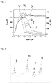
- Figure 7 schematically shows turn off waveforms measured at reverse-bias safe operating area (RBSOA) conditions, which are applying a maximum voltage of 1300 V and 300 A at 175 °C for three different 1700 V semiconductor devices, each provided with a structure 1 according to an embodiment.
- RSOA reverse-bias safe operating area
- the device depicted by "S” and “V” are produced with one injection step and one incomplete annealing step.
- the defect layer 5 of the device depicted by "T” and “W” as well as “U” and “X” are produced with two injection steps and two annealing steps.
- the further first dopants are introduced in the semiconductor film with a dose of 1 ⁇ 10 13 cm -2 .
- the further first dopants are introduced in the semiconductor film with a dose of 5 ⁇ 10 13 cm -2 .
- the further first dopants are formed of, e.g., Boron.
- the measuring point cluster depicted by "a” corresponds to structures 1 of four semiconductor devices, which are produced with one injection step and one incomplete annealing step.
- the first dopants are incorporated with a dose from at least 10 13 cm -2 and at most 5 10 16 cm -2 .
- the structures 1 are annealed with an incomplete laser process having energies of 1.5 J for the device on the first position from the left, 2.0 J for the device on the second position from the left, 2.5 J for the device on the third position from the left and 3.0 J for the device on the fourth position from the left.
- the measuring point cluster depicted by "b” corresponds to structures 1 of four semiconductor devices, which are produced with two injection steps and two annealing steps. Further first dopants are incorporated, e.g., Boron, in the semiconductor film in order to produce the defect layer 5, in comparison to the devices depicted by "a".
- first dopants e.g., Boron
- the measuring point cluster depicted by "c” corresponds to structures 1 of four semiconductor devices, which are produced similarly to the devices depicted by "a".
- first dopants are incorporated in the semiconductor film in order to produce the defect layer 5 having a dose being higher than a dose of the first dopants in connection with the devices depicted by "a".
- the measuring point cluster depicted by “d” corresponds to structures 1 of four semiconductor devices, which are produced similarly to the devices depicted by “b".
- first dopants are incorporated with a first incorporation step in the semiconductor film in order to produce the defect layer 5 having a dose being higher than a dose of the first dopants in connection with the devices depicted by "b".
- Figure 9 shows the SRPs of seven structures 1 of different semiconductor devices.
- the contact layers 4 and the defect layers 5 of the devices are produced with different annealing energies of the laser process.
- the doses for incorporating the first dopants and the further first are higher.
- the region indicated by "Y" corresponds to a SRP of a device, which is produced having a higher dose of further first dopants than the device depicted by "N" in Figure 5 .
- Figure 10 shows the SRPs of four structures 1 of different semiconductor devices, wherein the dose of the first dopants is greater than 10 15 cm -2 and the dose of the further first dopants is greater than 10 15 cm -2 .
- a base layer 2 and a semiconductor film being arranged on the base layer 2 are provided 100.
- first dopants are introduced 200 to the semiconductor film.
- the semiconductor film is heated 300 at least in regions such that a contact layer 4 and a defect layer 5 is generated 400 at least in regions.
- the contact layer 4 and the defect layer 5 are of a first conductivity type and the base layer 2 is of a second conductivity type.
- a concentration of the first dopants of the contact layer 4 being activated is higher than a concentration of the first dopants of the defect layer 5 being activated.
Landscapes
- Recrystallisation Techniques (AREA)
- Electrodes Of Semiconductors (AREA)
Abstract
- a contact layer (4) comprising first dopants of a first conductivity type,
- a base layer (2) of a second conductivity type, and
- a defect layer (5) comprising first dopants of the first conductivity type, wherein
- a concentration of the first dopants being activated in the contact layer (4) is higher than a concentration of the first dopants being activated in the defect layer (5).
Description
- The disclosure relates to a structure for a semiconductor device and a method for producing a structure for a semiconductor device.
- Semiconductor devices are used in many technical areas. Design optimization of such power semiconductor devices is often coupled with an optimization of an injection efficiency of at least one of an anode layer and a cathode layer. Control of the injection efficiency is generally achieved by varying dopant doses.
- Embodiments of the disclosure address in whole or in part the above shortcomings by a structure for a semiconductor device, which has an improved injection efficiency and by a method for producing such a structure.
- The exemplary embodiment of the disclosure addresses the above shortcomings by the subject-matter of the independent claims. Further embodiments are evident from the dependent claims and the following description.
- The first aspect of the disclosure relates to a structure for a semiconductor device. The semiconductor device is, for example, a diode, an insulated gate bipolar transistor, abbreviated as IGBT or a metal-oxide-semiconductor field-effect transistor, abbreviated as MOSFET. Exemplarily, the semiconductor device is, for example, a Non-Punch-Through (NPT) device or a Soft-Punch-Through (SPT) device.
- The semiconductor device is, for example, a power semiconductor device. The term "power" here and in the following, for example, refers to power semiconductor devices adapted for processing voltages and currents of more than 100 V and/or more than 10 A, exemplary voltages up to 1200 V and currents of several hundred amperes.
- According to the embodiment of the first aspect, the structure comprises a contact layer comprising first dopants of a first conductivity type. The contact layer comprises or consists, for example, of a semiconductor material. For example, the contact layer comprises first dopants, such as p-type dopants. In this case the first conductivity type is a p-type conductivity. Alternatively, the contact layer comprises first dopants being n-type dopants such that the first conductivity type is an n-type conductivity. Exemplarily, the contact layer is externally contactable in an electrical conductive manner.
- The contact layer has, for example, a main extension plane. For example, lateral directions are aligned parallel to the main extension plane and a vertical direction is aligned perpendicular to the main extension plane.
- According to the embodiment, the structure comprises a base layer of a second conductivity type different than the first conductivity type. The base layer comprises or consists of a semiconductor material, which is, for example, the same material than the semiconductor material of the contact layer. The second conductivity type is, for example, an n-type conductivity. Alternatively, the second conductivity type is a p-type conductivity. Exemplarily the second conductivity type is different from the first conductivity type. This is to say that if the contact layer is of a p-conductivity type, the base layer is of an n-conductivity type and vice versa.
- For example, the base layer does not comprise the first dopants. Exemplarily, the base layer is completely free of the first dopants.
- According to the embodiment, the structure comprises a defect layer comprising first dopants of the first conductivity type, wherein a concentration of the first dopants being activated in the contact layer is higher than a concentration of the first dopants being activated in the defect layer.
- The defect layer comprises or consists of a semiconductor material exemplarily being the same semiconductor material than the semiconductor material of the contact layer. For example, the concentration of the first dopants being activated decreases from the contact layer to the defect layer continuously.
- The first dopants exemplarily contribute to electronic properties of the contact layer and the defect layer, such as the conductivity. Further, due to the contribution of the first dopants to the electronic properties, for example, also an injection efficiency is dependent on the first dopants. Thus, the injection efficiency can be pre-set depending on the first dopants.
- At least some of the first dopants can be located exemplarily at interstitial lattice sites of at least one of the contact layer and the defect layer. Further, at least some of the first dopants can be located exemplarily at substitutional lattice sites of at least one of the contact layer and the defect layer.
- The first dopants are introduced exemplarily by an implantation process. The implantation process destroys, for example, a long range order of a crystal lattice of at least one of the contact layer and the defect layer. Thus, the injection increases an amorphousness of the crystal lattice of at least one of the contact layer and the defect layer.
- If at least some of the first dopants are located at interstitial lattice sites, sites in the crystal lattice of at least one of the contact layer and the defect layer are occupied by the first dopants, at which there is usually not an atom. The amorphousness of at least one of the contact layer and the defect layer increases, for example, if the number of first dopants located at interstitial lattice sites increases and vice versa.
- If at least some of the first dopants are located at substitutional lattice sides, sites in the crystal lattice of at least one of the contact layer and the defect layer are occupied by the first dopants, at which there is usually an atom. Thus, the first dopants are incorporated at a regular site in the crystal structure. For example, the amorphousness of at least one of the contact layer and the defect layer decreases, for example, if the number of first dopants located at substitutional lattice sites increases and vice versa.
- For example, if the amorphousness of at least one of the contact layer and the defect layer increases, the injection efficiency of at least one of the contact layer and the defect layer decreases and vice versa.
- For example, the first dopants being activated are located exemplarily at substitutional lattice sites. Furthermore, the first dopants being not activated are located exemplarily at interstitial lattice sites, for example.
- The concentration of the first dopants being activated in the contact layer is, for example, at least 10%, exemplarily 50%, higher than the concentration of the first dopants being activated in the defect layer.
- Exemplarily, the concentration of the first dopants being activated in the contact layer is at least 1·1018 cm-3. The concentration of the first dopants being activated within the defect layer is, for example, at most 1·1017 cm-3.
- In summary, such a structure for a semiconductor device can provide, inter alia, the following advantage. Exemplarily, the injection efficiency of the structure can be preset by the concentration of the first dopants being activated in the contact layer and the defect layer. With such a combination of the contact layer and the defect layer, the injection efficiency can be pre-set according to the needs of the semiconductor device.
- According to at least one embodiment of the structure, the defect layer is provided between the contact layer and the base layer at least in regions. For example, the base layer, the defect layer and the contact layer are stacked above one another in vertical direction in the order indicated. For example, the defect layer is in direct contact to the base layer.
- Exemplarily, the defect layer is provided completely between the contact layer and the base layer. In this case, the defect layer covers a main surface of the contact layer facing the defect layer completely.
- Alternatively, the defect layer does not cover the main surface of the contact layer completely. In this case, the defect layer has a cross sectional shape in lateral directions being circular, elliptical or polygonal. Furthermore, the defect layer can be located solely in regions of grid points of a grid, for example. The defect layer has at the grid points the cross sectional shape in lateral directions being circular, elliptical or polygonal.
- For example, the contact layer and the defect layer have a difference of the concentrations of the first dopants being activated. Exemplarily, the defect layer extends up to a boundary, wherein the boundary extends in lateral directions and is located between the contact layer and the defect layer in vertical direction. For example, the concentration of the first dopants being activated in the defect layer rises up to 50% of the difference at the boundary. Analogously, the concentration of the first dopants being activated in the contact layer drops down to 50% of the difference at the boundary.
- According to at least one embodiment of the structure, the defect layer is provided between the contact layer and the base layer, at least in regions. For example, the base layer, the contact layer and the defect layer are stacked above one another in vertical direction in the order indicated. In this embodiment, the contact layer is, for example, in direct contact to the base layer. In this case, the defect layer is configured for external contacting. Thus, the defect layer is, in this embodiment, configured to be externally contactable in an electrical conductive manner.
- According to at least one embodiment of the structure, a defect concentration in the contact layer is less than a defect concentration in the defect layer. For example, at least some of the first dopants form crystallographic defects in at least one of the contact layer and the defect layer. Crystallographic defects are exemplarily interruptions of the crystal lattice of at least one of the contact layer and the defect layer such as atoms located at interstitial sites of the crystal lattice. Furthermore, crystallographic defects can be formed from vacancy defects. A vacancy defect is exemplarily a vacant lattice site in the crystal lattice of at least one of the contact layer and the defect layer. For example, the defect concentration accounts all the crystallographic defects.
- Furthermore, the injection efficiency of at least one of the contact layer and the defect layer is dependent to the defect concentration. If the defect concentration is increased, for example, the injection efficiency decreases and vice versa.
- The defect concentration in the defect layer is, for example, at least 10%, exemplarily 50%, higher than the defect concentration of the first dopants being activated in the defect layer.
- According to at least one embodiment of the structure, a buffer layer of the second conductivity type is provided between the contact layer and the defect layer and the base layer. The buffer layer comprises or consists of a semiconductor material. In this embodiment, the base layer is in direct contact to the buffer layer.
- For example, the buffer layer is higher doped. Exemplary, the base layer has a homogeneous doping concentration and the buffer layer has a higher doping concentration than the homogeneous doping concentration of the base layer.
- For example, the base layer, the buffer layer, the defect layer and the contact layer are stacked above one another in vertical direction in the order indicated. In this case, the buffer layer is in direct contact to the defect layer.
- Alternatively, the base layer, the buffer layer, the contact layer and the defect layer are stacked above one another in vertical direction in the order indicated. In this case, the buffer layer is in direct contact to the contact layer.
- According to at least one embodiment of the structure, the contact layer and the defect layer are at least one of an anode layer and a cathode layer for a semiconductor device. For example, the at least one of an anode layer and a cathode layer is configured to be contacted with a metallization. Exemplarily, at least one of an anode layer and a cathode layer is freely accessible from an outside.
- A second aspect of the disclosure relates to a semiconductor device. The semiconductor device comprises a structure disclosed herein before. Thus, all features disclosed in connection with the structure are also disclosed in connection with the semiconductor device and vice versa.
- A third aspect of the disclosure relates to a method for producing a structure for a semiconductor device. For example, the method produces a structure for a semiconductor device described herein above. All features disclosed in connection with the structure are therefore also disclosed in connection with the method and vice versa.
- According to the embodiment of the second aspect of the method, a base layer and a semiconductor film being arranged on the base layer are provided. Exemplarily, the semiconductor film is grown epitaxially on the base layer.
- According to the embodiment of the method, first dopants are introduced to the semiconductor film. For example, the first dopants are injected in the semiconductor film. Exemplarily, first dopants are introduced to the semiconductor film up to a certain depth. For example, the depth is smaller than a thickness of the semiconductor film in vertical direction. Alternatively, the depth equals the thickness of the semiconductor film in vertical direction.
- According to the embodiment of the method, the semiconductor film is heated at least in regions such that a contact layer and a defect layer are generated at least in regions. Exemplarily, due to the heating, at least some of the first dopants can move from interstitial lattice sites to substitutional lattice sites.
- For example, the method steps are carried out in the following order: providing a base layer and a semiconductor film being arranged on the base layer, introducing first dopants to the semiconductor film, heating the semiconductor film at least in regions.
- According to the embodiment of the method, the contact layer and the defect layer are of a first conductivity type and the base layer is of a second conductivity type.
- According to the embodiment of the method, a concentration of the first dopants of the first contact layer being activated is higher than a concentration of the first dopants of the defect layer being activated.
- According to at least one embodiment of the method, the heating is carried out by a laser process. For example, during the laser process, laser light is applied to the semiconductor film.
- Exemplarily the laser light has an energy from at least 0.5 joules to at most 8 J. The laser light comprises, for example, a peak wavelength of at least 490 nm and at most 575 nm. A penetration depth of the laser light into the semiconductor film is dependent to the peak wavelength. The penetration depth of the laser light into the semiconductor film is, for example, at least 0.01 µm and at most 10 µm.
- According to at least one embodiment of the method, the laser process is applied at least in regions to an outer surface of the semiconductor film. For example, the outer surface faces away from the base layer. Exemplarily, the cross sectional shape in lateral directions of the defect layer is dependent to the cross sectional shape in lateral directions of the beam of the laser light.
- Exemplarily, the laser light can be applied to the outer surface of the semiconductor film completely such that the outer surface covered by the laser light completely.
- Alternatively, the laser light can be applied to the outer surface of the semiconductor film at grid points of a grid. In this case, the generated defect layer has at the grid points the cross sectional shape in lateral directions of a cross sectional shape in lateral directions of a beam of the laser light.
- According to at least one embodiment of the method, the laser process is an incomplete annealing process such that the defect layer is generated between the base layer and the contact layer. For example, the laser light of the laser process has the penetration depth in vertical direction into the semiconductor film being proportional to the peak wavelength of the laser light. Exemplarily at least some of the first dopants introduced in the semiconductor film are moved from interstitial lattice sides to substitutional lattice sides in a region in vertical direction from the outer surface of the semiconductor film up to the penetration depth. The semiconductor film is annealed properly within this region.
- In this embodiment, a region of the semiconductor film closer to the outer surface being annealed properly forms the connection layer and a region of the semiconductor film closer to the base layer being not annealed forms the defect layer.
- According to at least one embodiment of the method, the first dopants are introduced to the semiconductor film with a dose of at least 1·1014cm-2. Exemplarily, the first dopants are introduced to the semiconductor film with a dose of at least 1·1015cm-2. For example, first dopants comprise or consists of at least one of Boron and Phosphorous.
- According to at least one embodiment of the method, a first heating step is applied to the semiconductor film after the introduction of the first dopants. For example, the semiconductor film is heated to at least 900 °C in the first heating step. Exemplarily, within this step the whole semiconductor film with the first dopants is annealed such that at least some of the first dopants move from interstitial to substitutional lattice sides in the semiconductor film.
- Within this step, an amorphousness of the semiconductor film is exemplarily decreased as a whole, for example.
- According to at least one embodiment of the method, further first dopants are introduced to the semiconductor film after the first heating step. Exemplary, the further first dopants are the same dopants than the first dopants. Alternatively, the further first dopants comprise a different material than the first dopants.
- The further first dopants are introduced to the semiconductor film, e.g., up to a depth being less than the thickness of the semiconductor film in vertical direction. Alternatively, the further first dopants are introduced to the semiconductor film, e.g., up to a depth being equal to the thickness of the semiconductor film in vertical direction.
- If the first dopants are introduced in the semiconductor film up to the depth being smaller than the thickness of the semiconductor film in vertical direction, the further first dopants are introduced to the semiconductor film up to a depth being larger than the depth of the first dopants in vertical direction.
- In the case the further first dopants are introduced in the semiconductor film up to the depth being smaller than depth of the first dopants, a region of the semiconductor film closer to the outer surface comprises the further first dopants and a region of the semiconductor film closer to the base layer is free of the further first dopants. Exemplarily, an amorphousness of the semiconductor film is increased in the region closer to the outer surface.
- In the case the further first dopants are introduced in the semiconductor film up to the depth being larger than the depth of the first dopants, a region of the semiconductor film closer to the outer surface comprises the further first dopants and the first dopants being activated and a region of the semiconductor film closer to the base layer comprises the further first dopants. Exemplarily, an amorphousness of the semiconductor film is increased in the region closer to the base layer.
- According to at least one embodiment of the method, the further first dopants are introduced to the semiconductor film with a dose of at most 1·1014cm-2. The further first dopants are introduced to the semiconductor film with an applied energy of at most 100 keV. For example, the further first dopants comprise or consists of at least one of Boron and Phosphorous.
- According to at least one embodiment of the method, a second heating step is applied to the semiconductor film such that the defect layer is generated. For example, the semiconductor film is heated in the second heating step to at most 500 °C. Exemplarily, at least some of the further first dopants move from interstitial to substitutional lattice sides in the semiconductor film due to the second heating step. In this case, the moving is not as efficient as compared to the first heating step. Thus, comparatively less further first dopants move from interstitial to substitutional lattice sides.
- Exemplarily, the region of the semiconductor film closer to the outer surface comprising the further first dopants forms the defect region and the region of the semiconductor film closer to the base layer being free of the further first dopants forms the contact layer.
- Alternatively, the region of the semiconductor film closer to the base layer comprising the further first dopants forms the defect region and the region of the semiconductor film closer to the base layer comprising the first dopants and the further first dopants forms the contact layer.
- According to at least one embodiment of the method, the first heating step is a laser process or a furnace process.
- According to at least one embodiment of the method, the second heating step is a sintering process.
- For example, a metallization is provided on the outer surface of the semiconductor film. Exemplarily, the metallization comprises or consists of a metal. For example this metallization can be provided on the outer surface of the semiconductor film by the sintering process.
- According to at least one embodiment of the method, a temperature of the first heating step is higher than a temperature of the second heating step.
- According to at least one embodiment of the method, a buffer layer is provided on the base layer. This is to say that a buffer layer is provided between the base layer and the contact layer.
- The subject-matter of the disclosure will be explained in more detail in the following with reference to exemplary embodiments which are illustrated in the attached drawings.
-
Figure 1 schematically shows a cross-sectional view of a structure according to prior art and an embodiment; -
Figures 2 and3 each exemplarily shows spreading resistance profiles of different structures according to different embodiments; -
Figure 4 exemplarily shows a technology curve of different structures according to different embodiments; -
Figure 5 exemplarily shows spreading resistance profiles of different structures according to different embodiments; -
Figure 6 exemplarily shows a technology curve of different structures according to different embodiments; -
Figure 7 exemplarily shows turn off wave forms of structures of a semiconductor device; -
Figure 8 exemplarily shows nominal on-state measurements of structures of a semiconductor device -
Figures 9 and 10 each exemplarily shows spreading resistance profiles of different structures according to different embodiments; -
Figure 10 schematically shows a flow diagram of a method for producing a structure for a semiconductor device according to an embodiment. - The reference symbols used in the drawings and their meanings are listed in summary form in the list of reference symbols. In principle, identical parts are provided with the same reference symbols in the figures.
- The structure shown on the top of
Figure 1 schematically shows astructure 1A of a semiconductor device according to the prior art. - The structure shown on the bottom of
Figure 1 shows astructure 1 of a semiconductor device according to an embodiment. - The
structure 1 ofFigure 1 comprises acontact layer 4 comprising first dopants of a first conductivity type and adefect layer 5 comprising first dopants of the first conductivity type. Thecontact layer 4 and thedefect layer 5 are arranged on abuffer layer 3 and abase layer 2. - The
contact layer 4, thedefect layer 5, thebuffer layer 3 and abase layer 2 are stacked above one another and are in direct contact to one another. Furthermore, a concentration of the first dopants being activated in thecontact layer 4 is higher than a concentration of the first dopants being activated in thedefect layer 5. - For example, a width of the
contact layer 4 is at most 5 µm. In this embodiment, a width of thedefect layer 5 is smaller than the width of thecontact layer 4. - In
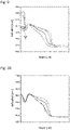
Figure 2 , spreading resistance profiles (SRPs) of fourdifferent structures 1 are shown. A SRP represents a measurement of a resistivity of a semiconducting device with astructure 1, as a function of a position. The measured resistivity is proportional to a carrier density being activated, i.e. the number of electrically active electrons or holes in a given volume. Thus, the SRP is proportional to a concentration of the first dopants being activated depicted by "ActiveNet" in cm-3. The range of the x-Axis forFigures 2 ,3 and5 is from 0 µm to 3 µm and forFigures 9 and 10 from 0 µm to 2.5 µm. - A
contact layer 4 and adefect layer 5 of thestructures 1 are used as an anode layer in a semiconductor device. The first dopants are in this case Boron and Phosphorous. Furthermore, the fourdifferent structures 1 have all the same buffer layers 3. - The buffer layers 3 are of a second conductivity type and, for example, are generated by ion implantation of second dopants. The second dopants of the buffer layers 3 are activated, for example, by laser process.
- The
contact layer 4 and thedefect layer 5 are generated by initially incorporating first dopants to a semiconductor film. The dose of the first dopants is the same for the fourstructures 1. - The first dopants in the
contact layer 4 and thedefect layer 5 of thestructures 1 are activated by a laser process, being an incomplete laser annealing process, using four different laser energies from 1.1 Joules to 1.4 Joules - and thereby generating thecontact layer 4 and thedefect layer 5 having a combined injection efficiency being different for all the fourstructures 1. - The SRP having the lowest concentration at 1 µm corresponds to a laser energy of 1.1 J. The SRP having the second lowest concentration at 1 µm, i.e. at the fourth tick of the x-axis - corresponds to a laser energy of 1.4 J, the SRP having the third lowest concentration at 1 µm corresponds to a laser energy of 1.2 J and the SRP having the highest concentration at 1 µm corresponds to a laser energy of 1.3 J.
-
Figure 3 shows the SRPs of twostructures 1. Thestructure 1 in connection with the SRP "E" is produced by only one heating step. However, thecontact layer 4 and thedefect layer 5 of thestructure 1 in connection with the SRP "F" are generated by incorporating first dopants to a semiconductor film followed by a first heating step and an incorporation of further first dopants to the semiconductor film followed by a second heating step. -
Figure 4 shows a turn-off loss Eoff in mJ depending to a collector-emitter voltage Vce in V fordifferent structures 1. Such a representation is also called "technology curve". - First dopants are incorporated in the semiconductor film of the
structures 1 of semiconductor devices corresponding to "G" and "I" with a dose of 1·1015 cm-2. Further, first dopants are incorporated in the semiconductor film of thestructures 1 of devices corresponding to "H" and "J" with a dose of 5·1015 cm-2. Subsequently, the semiconductor film of thestructures 1 corresponding to "G" and "H" are heated by an incomplete annealing process with an energy of 1.3 J - thereby generating thecontact layer 4 and thedefect layer 5. In addition, the semiconductor film of thestructures 1 corresponding to "I" and "J" are heated subsequently by an incomplete annealing process with an energy of 1.1 J - thereby generating thecontact layer 4 and thedefect layer 5. - By having the same laser process energies, a
structure 1 of a semiconductor device treated with a higher dose has a higher on-state due to the incomplete annealing of defects during the laser annealing process. Thus, the injection efficiency decreases, that means the on-state increases, with an increase in the dose. -
Figure 5 shows the SRPs of sixstructures 1. The twostructures 1 corresponding to "L" are not provided with a further incorporation of further first dopants. The twostructures 1 corresponding to "M" are provided with a further incorporation of further first dopants with a dose of 1·1013 cm-2 using an energy of 25 keV. The twostructures 1 corresponding to "N" are provided with a further incorporation of further first dopants with a dose of 1·1014 cm-2 using an energy of 25 keV. - Furthermore, the three SRPs having the three concentrations at 1 µm each correspond to a laser energy of 1.6 J. The three SRPs having the three highest concentrations at 1 µm each correspond to a laser energy of 1.4 J.
-
Figure 6 shows the turn-off loss Eoff in mJ depending to the collector-emitter voltage Vce in V fordifferent structures 1. - The
structures 1 of different semiconductor devices depicted with a symbol being not filled, i.e. the device marked with "R", are annealed with a laser process having an energy of 1.6 J. Thestructures 1 of different devices depicted with a symbol being filled, i.e. the device marked with "Q", are annealed with a laser process having an energy of 1.4 J. The devices depicted by circles are produced with one injection step and one incomplete annealing step. The devices depicted by squares and triangles are produced with two injection steps and two annealing steps. The defect layers 5 of the devices depicted by squares are produced with a lower dose of further first dopants than the defect layers 5 of the devices depicted by triangles. -
Figure 7 schematically shows turn off waveforms measured at reverse-bias safe operating area (RBSOA) conditions, which are applying a maximum voltage of 1300 V and 300 A at 175 °C for three different 1700 V semiconductor devices, each provided with astructure 1 according to an embodiment. - The device depicted by "S" and "V" are produced with one injection step and one incomplete annealing step. The
defect layer 5 of the device depicted by "T" and "W" as well as "U" and "X" are produced with two injection steps and two annealing steps. For the device depicted by "T" and "W", the further first dopants are introduced in the semiconductor film with a dose of 1·1013cm-2. For the device depicted by "U" and "X", the further first dopants are introduced in the semiconductor film with a dose of 5·1013cm-2. The further first dopants are formed of, e.g., Boron. - The nominal on-state measurements of
structures 1 of different semiconductor devices are shown inFigure 8 . - The measuring point cluster depicted by "a" corresponds to
structures 1 of four semiconductor devices, which are produced with one injection step and one incomplete annealing step. The first dopants are incorporated with a dose from at least 1013 cm-2 and at most 5 1016 cm-2. Thestructures 1 are annealed with an incomplete laser process having energies of 1.5 J for the device on the first position from the left, 2.0 J for the device on the second position from the left, 2.5 J for the device on the third position from the left and 3.0 J for the device on the fourth position from the left. - The measuring point cluster depicted by "b" corresponds to
structures 1 of four semiconductor devices, which are produced with two injection steps and two annealing steps. Further first dopants are incorporated, e.g., Boron, in the semiconductor film in order to produce thedefect layer 5, in comparison to the devices depicted by "a". - The measuring point cluster depicted by "c" corresponds to
structures 1 of four semiconductor devices, which are produced similarly to the devices depicted by "a". In comparison, first dopants are incorporated in the semiconductor film in order to produce thedefect layer 5 having a dose being higher than a dose of the first dopants in connection with the devices depicted by "a". - The measuring point cluster depicted by "d" corresponds to
structures 1 of four semiconductor devices, which are produced similarly to the devices depicted by "b". In comparison, first dopants are incorporated with a first incorporation step in the semiconductor film in order to produce thedefect layer 5 having a dose being higher than a dose of the first dopants in connection with the devices depicted by "b". -
Figure 9 shows the SRPs of sevenstructures 1 of different semiconductor devices. The contact layers 4 and the defect layers 5 of the devices are produced with different annealing energies of the laser process. In comparison toFigure 5 , the doses for incorporating the first dopants and the further first are higher. In a depth range from 0.0 µm to 0.5 µm, the region indicated by "Y" corresponds to a SRP of a device, which is produced having a higher dose of further first dopants than the device depicted by "N" inFigure 5 . -
Figure 10 shows the SRPs of fourstructures 1 of different semiconductor devices, wherein the dose of the first dopants is greater than 1015 cm-2 and the dose of the further first dopants is greater than 1015 cm-2. - According to
Figure 11 , initially abase layer 2 and a semiconductor film being arranged on thebase layer 2 are provided 100. Subsequently first dopants are introduced 200 to the semiconductor film. In a next step, the semiconductor film is heated 300 at least in regions such that acontact layer 4 and adefect layer 5 is generated 400 at least in regions. Here, thecontact layer 4 and thedefect layer 5 are of a first conductivity type and thebase layer 2 is of a second conductivity type. Further, a concentration of the first dopants of thecontact layer 4 being activated is higher than a concentration of the first dopants of thedefect layer 5 being activated. -
- 1
- structure
- 1A
- structure according to prior art
- 2
- base layer
- 3
- buffer layer
- 4
- contact layer
- 5
- defect layer
- a-d
- measuring point cluster
- E-F
- SRP
- G-J
- structures corresponding to measurement point
- L-P
- SRPs
- Q, R
- structures corresponding to measurement point
- S-X
- structures corresponding to measurement point
- Y
- region of SRP
Claims (15)
- A structure (1) for a semiconductor device, with- a contact layer (4) comprising first dopants of a first conductivity type,- a base layer (2) of a second conductivity type different than the first conductivity type, and- a defect layer (5) comprising first dopants of the first conductivity type, wherein- a concentration of the first dopants being activated in the contact layer (4) is higher than a concentration of the first dopants being activated in the defect layer (5).
- The structure (1) according to the preceding claim, wherein
the defect layer (5) is provided between the contact layer (4) and the base layer (2) at least in regions. - The structure (1) according to claim 1, wherein
the contact layer (4) is provided between the defect layer (5) and the base layer (2). - The structure (1) according to one of the preceding claims, wherein a defect concentration in the contact layer (4) is less than a defect concentration in the defect layer (5) .
- The structure (1) according to one of the preceding claims, wherein a buffer layer (3) of the second conductivity type is provided between the contact layer (4) as well as the defect layer (5) and the base layer (2).
- The structure (1) according to one of the preceding claims, wherein the contact layer (4) and the defect layer (5) are at least one of an anode layer and a cathode layer for a semiconductor device.
- A semiconductor device comprising a structure (1) according to one of the preceding claims.
- A method for producing a structure (1) for a semiconductor device comprising:- providing a base layer (2) and a semiconductor film being arranged on the base layer (2),- introducing first dopants to the semiconductor film,- heating the semiconductor film at least in regions such that a contact layer (4) and a defect layer (5) are generated at least in regions, wherein- the contact layer (4) and the defect layer (5) are of a first conductivity type and the base layer (2) is of a second conductivity type, and- a concentration of the first dopants of the contact layer (4) being activated is higher than a concentration of the first dopants of the defect layer (5) being activated.
- The method according to claim 8, wherein- the heating is carried out by a laser process,- the laser process is applied at least in regions to an outer surface of the semiconductor film, and- the laser process is an incomplete annealing process such that the defect layer (5) is generated between the base layer (2) and the contact layer (4).
- The method according to claim 9, wherein the first dopants are introduced to the semiconductor film with a dose of at least 1·1014 cm-2.
- The method according to claim 8, wherein the heating comprises at least two heating steps, wherein- after the introduction of the first dopants, a first heating step is applied to the semiconductor film,- after the first heating step, further first dopants are introduced to the semiconductor film,- after the introduction of the further first dopants, a second heating step is applied to the semiconductor film such that the defect layer (5) is generated.
- The method according to claim 11, the further first dopants are introduced to the semiconductor film with a dose of at most 1·1014cm-2.
- The method according to claim 11 or 12, wherein- the first heating step is a laser process or a furnace process, and- the second heating step is a sintering process.
- The method according to one of claims 11 to 13, wherein a temperature of the first heating step is higher than a temperature of the second heating step.
- The method according to one of claims 8 to 14, wherein a buffer layer (3) is provided on the base layer (2).
Priority Applications (5)
| Application Number | Priority Date | Filing Date | Title |
|---|---|---|---|
| EP20214245.1A EP4016647B1 (en) | 2020-12-15 | 2020-12-15 | Structure for a semiconductor device and method for producing a structure for a semiconductor device |
| JP2023536135A JP2023554043A (en) | 2020-12-15 | 2021-12-13 | Structure for a semiconductor device and method for manufacturing a structure for a semiconductor device |
| DE212021000522.5U DE212021000522U1 (en) | 2020-12-15 | 2021-12-13 | Structure for a semiconductor device |
| PCT/EP2021/085481 WO2022128913A1 (en) | 2020-12-15 | 2021-12-13 | Structure for a semiconductor device and method for producing a structure for a semiconductor device |
| CN202180084410.7A CN116615797A (en) | 2020-12-15 | 2021-12-13 | Structure for semiconductor device and method of manufacturing structure for semiconductor device |
Applications Claiming Priority (1)
| Application Number | Priority Date | Filing Date | Title |
|---|---|---|---|
| EP20214245.1A EP4016647B1 (en) | 2020-12-15 | 2020-12-15 | Structure for a semiconductor device and method for producing a structure for a semiconductor device |
Publications (2)
| Publication Number | Publication Date |
|---|---|
| EP4016647A1 true EP4016647A1 (en) | 2022-06-22 |
| EP4016647B1 EP4016647B1 (en) | 2024-02-07 |
Family
ID=73854612
Family Applications (1)
| Application Number | Title | Priority Date | Filing Date |
|---|---|---|---|
| EP20214245.1A Active EP4016647B1 (en) | 2020-12-15 | 2020-12-15 | Structure for a semiconductor device and method for producing a structure for a semiconductor device |
Country Status (5)
| Country | Link |
|---|---|
| EP (1) | EP4016647B1 (en) |
| JP (1) | JP2023554043A (en) |
| CN (1) | CN116615797A (en) |
| DE (1) | DE212021000522U1 (en) |
| WO (1) | WO2022128913A1 (en) |
Citations (2)
| Publication number | Priority date | Publication date | Assignee | Title |
|---|---|---|---|---|
| US20150303268A1 (en) * | 2013-01-18 | 2015-10-22 | Hitachi Power Semiconductor Device, Ltd. | Diode and power conversion device |
| US20190058065A1 (en) * | 2017-08-18 | 2019-02-21 | Infineon Technologies Austria Ag | Power Diode and Method of Manufacturing a Power Diode |
Family Cites Families (3)
| Publication number | Priority date | Publication date | Assignee | Title |
|---|---|---|---|---|
| JPS58216473A (en) * | 1982-06-11 | 1983-12-16 | Hitachi Ltd | Diode |
| JP4123913B2 (en) * | 2001-11-26 | 2008-07-23 | 富士電機デバイステクノロジー株式会社 | Manufacturing method of semiconductor device |
| JP2012256628A (en) * | 2011-06-07 | 2012-12-27 | Renesas Electronics Corp | Igbt and diode |
-
2020
- 2020-12-15 EP EP20214245.1A patent/EP4016647B1/en active Active
-
2021
- 2021-12-13 WO PCT/EP2021/085481 patent/WO2022128913A1/en not_active Ceased
- 2021-12-13 JP JP2023536135A patent/JP2023554043A/en active Pending
- 2021-12-13 DE DE212021000522.5U patent/DE212021000522U1/en active Active
- 2021-12-13 CN CN202180084410.7A patent/CN116615797A/en active Pending
Patent Citations (2)
| Publication number | Priority date | Publication date | Assignee | Title |
|---|---|---|---|---|
| US20150303268A1 (en) * | 2013-01-18 | 2015-10-22 | Hitachi Power Semiconductor Device, Ltd. | Diode and power conversion device |
| US20190058065A1 (en) * | 2017-08-18 | 2019-02-21 | Infineon Technologies Austria Ag | Power Diode and Method of Manufacturing a Power Diode |
Also Published As
| Publication number | Publication date |
|---|---|
| CN116615797A (en) | 2023-08-18 |
| WO2022128913A1 (en) | 2022-06-23 |
| JP2023554043A (en) | 2023-12-26 |
| DE212021000522U1 (en) | 2023-08-30 |
| EP4016647B1 (en) | 2024-02-07 |
Similar Documents
| Publication | Publication Date | Title |
|---|---|---|
| US12317560B2 (en) | Semiconductor device | |
| US10950717B2 (en) | Semiconductor device having semiconductor regions with an impurity concentration distribution which decreases from a respective peak toward different semiconductor layers | |
| JP7271659B2 (en) | Insulated gate power semiconductor device and method for manufacturing such device | |
| KR20120104537A (en) | Semiconductor device and method for manufacturing semiconductor device | |
| JP2002305304A (en) | Power semiconductor device | |
| CN108074810B (en) | Method for manufacturing semiconductor device | |
| JPWO2020149354A1 (en) | Semiconductor devices and manufacturing methods for semiconductor devices | |
| US10074715B2 (en) | Semiconductor wafer, implantation apparatus for implanting protons and method for forming a semiconductor device | |
| JP5326217B2 (en) | Semiconductor device and manufacturing method thereof | |
| US6781156B2 (en) | Recombination center diffusion controlled by carbon concentration | |
| WO2020054446A1 (en) | Semiconductor device | |
| CA1144285A (en) | Ion implanted reverse-conducting thyristor | |
| JP2004247593A (en) | Semiconductor device and manufacturing method thereof | |
| EP4016647B1 (en) | Structure for a semiconductor device and method for producing a structure for a semiconductor device | |
| EP3240040A1 (en) | Insulated gate bipolar transistor and method for manufacturing such an insulated gate bipolar transistor | |
| US20220344467A1 (en) | 4h-sic mosfet device and manufacturing method thereof | |
| US11522047B2 (en) | Non-punch-through reverse-conducting power semiconductor device and method for producing same | |
| CN108321191B (en) | Power semiconductor device and method for manufacturing the same | |
| KR20120091197A (en) | Punch-through semiconductor device and method for producing same | |
| US20190115423A1 (en) | Insulated gate power devices with reduced carrier injection in termination area | |
| KR101928395B1 (en) | Power semiconductor device and manufacturing method thereof | |
| CN119631593A (en) | Semiconductor devices | |
| WO2024067998A1 (en) | Semiconductor device and manufacturing method | |
| CN121286119A (en) | MOSFET with injected charge compensation region | |
| CN119631592A (en) | Semiconductor devices |
Legal Events
| Date | Code | Title | Description |
|---|---|---|---|
| PUAI | Public reference made under article 153(3) epc to a published international application that has entered the european phase |
Free format text: ORIGINAL CODE: 0009012 |
|
| STAA | Information on the status of an ep patent application or granted ep patent |
Free format text: STATUS: THE APPLICATION HAS BEEN PUBLISHED |
|
| AK | Designated contracting states |
Kind code of ref document: A1 Designated state(s): AL AT BE BG CH CY CZ DE DK EE ES FI FR GB GR HR HU IE IS IT LI LT LU LV MC MK MT NL NO PL PT RO RS SE SI SK SM TR |
|
| STAA | Information on the status of an ep patent application or granted ep patent |
Free format text: STATUS: REQUEST FOR EXAMINATION WAS MADE |
|
| 17P | Request for examination filed |
Effective date: 20220810 |
|
| RBV | Designated contracting states (corrected) |
Designated state(s): AL AT BE BG CH CY CZ DE DK EE ES FI FR GB GR HR HU IE IS IT LI LT LU LV MC MK MT NL NO PL PT RO RS SE SI SK SM TR |
|
| STAA | Information on the status of an ep patent application or granted ep patent |
Free format text: STATUS: EXAMINATION IS IN PROGRESS |
|
| 17Q | First examination report despatched |
Effective date: 20221102 |
|
| P01 | Opt-out of the competence of the unified patent court (upc) registered |
Effective date: 20230527 |
|
| GRAP | Despatch of communication of intention to grant a patent |
Free format text: ORIGINAL CODE: EPIDOSNIGR1 |
|
| STAA | Information on the status of an ep patent application or granted ep patent |
Free format text: STATUS: GRANT OF PATENT IS INTENDED |
|
| RIC1 | Information provided on ipc code assigned before grant |
Ipc: H01L 21/268 20060101ALN20230705BHEP Ipc: H01L 29/32 20060101ALI20230705BHEP Ipc: H01L 21/329 20060101ALI20230705BHEP Ipc: H01L 29/861 20060101AFI20230705BHEP |
|
| INTG | Intention to grant announced |
Effective date: 20230809 |
|
| GRAS | Grant fee paid |
Free format text: ORIGINAL CODE: EPIDOSNIGR3 |
|
| RAP1 | Party data changed (applicant data changed or rights of an application transferred) |
Owner name: HITACHI ENERGY LTD |
|
| GRAA | (expected) grant |
Free format text: ORIGINAL CODE: 0009210 |
|
| STAA | Information on the status of an ep patent application or granted ep patent |
Free format text: STATUS: THE PATENT HAS BEEN GRANTED |
|
| AK | Designated contracting states |
Kind code of ref document: B1 Designated state(s): AL AT BE BG CH CY CZ DE DK EE ES FI FR GB GR HR HU IE IS IT LI LT LU LV MC MK MT NL NO PL PT RO RS SE SI SK SM TR |
|
| REG | Reference to a national code |
Ref country code: GB Ref legal event code: FG4D |
|
| REG | Reference to a national code |
Ref country code: CH Ref legal event code: EP |
|
| REG | Reference to a national code |
Ref country code: IE Ref legal event code: FG4D |
|
| REG | Reference to a national code |
Ref country code: DE Ref legal event code: R096 Ref document number: 602020025294 Country of ref document: DE |
|
| REG | Reference to a national code |
Ref country code: LT Ref legal event code: MG9D |
|
| REG | Reference to a national code |
Ref country code: NL Ref legal event code: MP Effective date: 20240207 |
|
| PG25 | Lapsed in a contracting state [announced via postgrant information from national office to epo] |
Ref country code: IS Free format text: LAPSE BECAUSE OF FAILURE TO SUBMIT A TRANSLATION OF THE DESCRIPTION OR TO PAY THE FEE WITHIN THE PRESCRIBED TIME-LIMIT Effective date: 20240607 |
|
| PG25 | Lapsed in a contracting state [announced via postgrant information from national office to epo] |
Ref country code: LT Free format text: LAPSE BECAUSE OF FAILURE TO SUBMIT A TRANSLATION OF THE DESCRIPTION OR TO PAY THE FEE WITHIN THE PRESCRIBED TIME-LIMIT Effective date: 20240207 |
|
| PG25 | Lapsed in a contracting state [announced via postgrant information from national office to epo] |
Ref country code: GR Free format text: LAPSE BECAUSE OF FAILURE TO SUBMIT A TRANSLATION OF THE DESCRIPTION OR TO PAY THE FEE WITHIN THE PRESCRIBED TIME-LIMIT Effective date: 20240508 |
|
| REG | Reference to a national code |
Ref country code: AT Ref legal event code: MK05 Ref document number: 1655928 Country of ref document: AT Kind code of ref document: T Effective date: 20240207 |
|
| PG25 | Lapsed in a contracting state [announced via postgrant information from national office to epo] |
Ref country code: HR Free format text: LAPSE BECAUSE OF FAILURE TO SUBMIT A TRANSLATION OF THE DESCRIPTION OR TO PAY THE FEE WITHIN THE PRESCRIBED TIME-LIMIT Effective date: 20240207 Ref country code: NL Free format text: LAPSE BECAUSE OF FAILURE TO SUBMIT A TRANSLATION OF THE DESCRIPTION OR TO PAY THE FEE WITHIN THE PRESCRIBED TIME-LIMIT Effective date: 20240207 Ref country code: RS Free format text: LAPSE BECAUSE OF FAILURE TO SUBMIT A TRANSLATION OF THE DESCRIPTION OR TO PAY THE FEE WITHIN THE PRESCRIBED TIME-LIMIT Effective date: 20240507 |
|
| PG25 | Lapsed in a contracting state [announced via postgrant information from national office to epo] |
Ref country code: ES Free format text: LAPSE BECAUSE OF FAILURE TO SUBMIT A TRANSLATION OF THE DESCRIPTION OR TO PAY THE FEE WITHIN THE PRESCRIBED TIME-LIMIT Effective date: 20240207 |
|
| PG25 | Lapsed in a contracting state [announced via postgrant information from national office to epo] |
Ref country code: AT Free format text: LAPSE BECAUSE OF FAILURE TO SUBMIT A TRANSLATION OF THE DESCRIPTION OR TO PAY THE FEE WITHIN THE PRESCRIBED TIME-LIMIT Effective date: 20240207 |
|
| PG25 | Lapsed in a contracting state [announced via postgrant information from national office to epo] |
Ref country code: RS Free format text: LAPSE BECAUSE OF FAILURE TO SUBMIT A TRANSLATION OF THE DESCRIPTION OR TO PAY THE FEE WITHIN THE PRESCRIBED TIME-LIMIT Effective date: 20240507 Ref country code: NO Free format text: LAPSE BECAUSE OF FAILURE TO SUBMIT A TRANSLATION OF THE DESCRIPTION OR TO PAY THE FEE WITHIN THE PRESCRIBED TIME-LIMIT Effective date: 20240507 Ref country code: NL Free format text: LAPSE BECAUSE OF FAILURE TO SUBMIT A TRANSLATION OF THE DESCRIPTION OR TO PAY THE FEE WITHIN THE PRESCRIBED TIME-LIMIT Effective date: 20240207 Ref country code: LT Free format text: LAPSE BECAUSE OF FAILURE TO SUBMIT A TRANSLATION OF THE DESCRIPTION OR TO PAY THE FEE WITHIN THE PRESCRIBED TIME-LIMIT Effective date: 20240207 Ref country code: IS Free format text: LAPSE BECAUSE OF FAILURE TO SUBMIT A TRANSLATION OF THE DESCRIPTION OR TO PAY THE FEE WITHIN THE PRESCRIBED TIME-LIMIT Effective date: 20240607 Ref country code: HR Free format text: LAPSE BECAUSE OF FAILURE TO SUBMIT A TRANSLATION OF THE DESCRIPTION OR TO PAY THE FEE WITHIN THE PRESCRIBED TIME-LIMIT Effective date: 20240207 Ref country code: GR Free format text: LAPSE BECAUSE OF FAILURE TO SUBMIT A TRANSLATION OF THE DESCRIPTION OR TO PAY THE FEE WITHIN THE PRESCRIBED TIME-LIMIT Effective date: 20240508 Ref country code: FI Free format text: LAPSE BECAUSE OF FAILURE TO SUBMIT A TRANSLATION OF THE DESCRIPTION OR TO PAY THE FEE WITHIN THE PRESCRIBED TIME-LIMIT Effective date: 20240207 Ref country code: ES Free format text: LAPSE BECAUSE OF FAILURE TO SUBMIT A TRANSLATION OF THE DESCRIPTION OR TO PAY THE FEE WITHIN THE PRESCRIBED TIME-LIMIT Effective date: 20240207 Ref country code: BG Free format text: LAPSE BECAUSE OF FAILURE TO SUBMIT A TRANSLATION OF THE DESCRIPTION OR TO PAY THE FEE WITHIN THE PRESCRIBED TIME-LIMIT Effective date: 20240207 Ref country code: AT Free format text: LAPSE BECAUSE OF FAILURE TO SUBMIT A TRANSLATION OF THE DESCRIPTION OR TO PAY THE FEE WITHIN THE PRESCRIBED TIME-LIMIT Effective date: 20240207 |
|
| PG25 | Lapsed in a contracting state [announced via postgrant information from national office to epo] |
Ref country code: PL Free format text: LAPSE BECAUSE OF FAILURE TO SUBMIT A TRANSLATION OF THE DESCRIPTION OR TO PAY THE FEE WITHIN THE PRESCRIBED TIME-LIMIT Effective date: 20240207 Ref country code: PT Free format text: LAPSE BECAUSE OF FAILURE TO SUBMIT A TRANSLATION OF THE DESCRIPTION OR TO PAY THE FEE WITHIN THE PRESCRIBED TIME-LIMIT Effective date: 20240607 |
|
| PG25 | Lapsed in a contracting state [announced via postgrant information from national office to epo] |
Ref country code: SE Free format text: LAPSE BECAUSE OF FAILURE TO SUBMIT A TRANSLATION OF THE DESCRIPTION OR TO PAY THE FEE WITHIN THE PRESCRIBED TIME-LIMIT Effective date: 20240207 Ref country code: PT Free format text: LAPSE BECAUSE OF FAILURE TO SUBMIT A TRANSLATION OF THE DESCRIPTION OR TO PAY THE FEE WITHIN THE PRESCRIBED TIME-LIMIT Effective date: 20240607 Ref country code: PL Free format text: LAPSE BECAUSE OF FAILURE TO SUBMIT A TRANSLATION OF THE DESCRIPTION OR TO PAY THE FEE WITHIN THE PRESCRIBED TIME-LIMIT Effective date: 20240207 Ref country code: LV Free format text: LAPSE BECAUSE OF FAILURE TO SUBMIT A TRANSLATION OF THE DESCRIPTION OR TO PAY THE FEE WITHIN THE PRESCRIBED TIME-LIMIT Effective date: 20240207 |
|
| PG25 | Lapsed in a contracting state [announced via postgrant information from national office to epo] |
Ref country code: DK Free format text: LAPSE BECAUSE OF FAILURE TO SUBMIT A TRANSLATION OF THE DESCRIPTION OR TO PAY THE FEE WITHIN THE PRESCRIBED TIME-LIMIT Effective date: 20240207 |
|
| PG25 | Lapsed in a contracting state [announced via postgrant information from national office to epo] |
Ref country code: SM Free format text: LAPSE BECAUSE OF FAILURE TO SUBMIT A TRANSLATION OF THE DESCRIPTION OR TO PAY THE FEE WITHIN THE PRESCRIBED TIME-LIMIT Effective date: 20240207 |
|
| PG25 | Lapsed in a contracting state [announced via postgrant information from national office to epo] |
Ref country code: EE Free format text: LAPSE BECAUSE OF FAILURE TO SUBMIT A TRANSLATION OF THE DESCRIPTION OR TO PAY THE FEE WITHIN THE PRESCRIBED TIME-LIMIT Effective date: 20240207 Ref country code: CZ Free format text: LAPSE BECAUSE OF FAILURE TO SUBMIT A TRANSLATION OF THE DESCRIPTION OR TO PAY THE FEE WITHIN THE PRESCRIBED TIME-LIMIT Effective date: 20240207 |
|
| PG25 | Lapsed in a contracting state [announced via postgrant information from national office to epo] |
Ref country code: SK Free format text: LAPSE BECAUSE OF FAILURE TO SUBMIT A TRANSLATION OF THE DESCRIPTION OR TO PAY THE FEE WITHIN THE PRESCRIBED TIME-LIMIT Effective date: 20240207 |
|
| PG25 | Lapsed in a contracting state [announced via postgrant information from national office to epo] |
Ref country code: SM Free format text: LAPSE BECAUSE OF FAILURE TO SUBMIT A TRANSLATION OF THE DESCRIPTION OR TO PAY THE FEE WITHIN THE PRESCRIBED TIME-LIMIT Effective date: 20240207 Ref country code: SK Free format text: LAPSE BECAUSE OF FAILURE TO SUBMIT A TRANSLATION OF THE DESCRIPTION OR TO PAY THE FEE WITHIN THE PRESCRIBED TIME-LIMIT Effective date: 20240207 Ref country code: RO Free format text: LAPSE BECAUSE OF FAILURE TO SUBMIT A TRANSLATION OF THE DESCRIPTION OR TO PAY THE FEE WITHIN THE PRESCRIBED TIME-LIMIT Effective date: 20240207 Ref country code: EE Free format text: LAPSE BECAUSE OF FAILURE TO SUBMIT A TRANSLATION OF THE DESCRIPTION OR TO PAY THE FEE WITHIN THE PRESCRIBED TIME-LIMIT Effective date: 20240207 Ref country code: DK Free format text: LAPSE BECAUSE OF FAILURE TO SUBMIT A TRANSLATION OF THE DESCRIPTION OR TO PAY THE FEE WITHIN THE PRESCRIBED TIME-LIMIT Effective date: 20240207 Ref country code: CZ Free format text: LAPSE BECAUSE OF FAILURE TO SUBMIT A TRANSLATION OF THE DESCRIPTION OR TO PAY THE FEE WITHIN THE PRESCRIBED TIME-LIMIT Effective date: 20240207 |
|
| REG | Reference to a national code |
Ref country code: DE Ref legal event code: R097 Ref document number: 602020025294 Country of ref document: DE |
|
| REG | Reference to a national code |
Ref country code: DE Ref legal event code: R079 Ref document number: 602020025294 Country of ref document: DE Free format text: PREVIOUS MAIN CLASS: H01L0029861000 Ipc: H10D0008000000 |
|
| PG25 | Lapsed in a contracting state [announced via postgrant information from national office to epo] |
Ref country code: IT Free format text: LAPSE BECAUSE OF FAILURE TO SUBMIT A TRANSLATION OF THE DESCRIPTION OR TO PAY THE FEE WITHIN THE PRESCRIBED TIME-LIMIT Effective date: 20240207 |
|
| PLBE | No opposition filed within time limit |
Free format text: ORIGINAL CODE: 0009261 |
|
| STAA | Information on the status of an ep patent application or granted ep patent |
Free format text: STATUS: NO OPPOSITION FILED WITHIN TIME LIMIT |
|
| PG25 | Lapsed in a contracting state [announced via postgrant information from national office to epo] |
Ref country code: IT Free format text: LAPSE BECAUSE OF FAILURE TO SUBMIT A TRANSLATION OF THE DESCRIPTION OR TO PAY THE FEE WITHIN THE PRESCRIBED TIME-LIMIT Effective date: 20240207 |
|
| 26N | No opposition filed |
Effective date: 20241108 |
|
| PG25 | Lapsed in a contracting state [announced via postgrant information from national office to epo] |
Ref country code: SI Free format text: LAPSE BECAUSE OF FAILURE TO SUBMIT A TRANSLATION OF THE DESCRIPTION OR TO PAY THE FEE WITHIN THE PRESCRIBED TIME-LIMIT Effective date: 20240207 |
|
| PG25 | Lapsed in a contracting state [announced via postgrant information from national office to epo] |
Ref country code: MC Free format text: LAPSE BECAUSE OF FAILURE TO SUBMIT A TRANSLATION OF THE DESCRIPTION OR TO PAY THE FEE WITHIN THE PRESCRIBED TIME-LIMIT Effective date: 20240207 |
|
| REG | Reference to a national code |
Ref country code: CH Ref legal event code: PL |
|
| PG25 | Lapsed in a contracting state [announced via postgrant information from national office to epo] |
Ref country code: LU Free format text: LAPSE BECAUSE OF NON-PAYMENT OF DUE FEES Effective date: 20241215 |
|
| GBPC | Gb: european patent ceased through non-payment of renewal fee |
Effective date: 20241215 |
|
| REG | Reference to a national code |
Ref country code: BE Ref legal event code: MM Effective date: 20241231 |
|
| PG25 | Lapsed in a contracting state [announced via postgrant information from national office to epo] |
Ref country code: BE Free format text: LAPSE BECAUSE OF NON-PAYMENT OF DUE FEES Effective date: 20241231 Ref country code: GB Free format text: LAPSE BECAUSE OF NON-PAYMENT OF DUE FEES Effective date: 20241215 |
|
| PG25 | Lapsed in a contracting state [announced via postgrant information from national office to epo] |
Ref country code: FR Free format text: LAPSE BECAUSE OF NON-PAYMENT OF DUE FEES Effective date: 20241231 |
|
| PG25 | Lapsed in a contracting state [announced via postgrant information from national office to epo] |
Ref country code: CH Free format text: LAPSE BECAUSE OF NON-PAYMENT OF DUE FEES Effective date: 20241231 |
|
| PG25 | Lapsed in a contracting state [announced via postgrant information from national office to epo] |
Ref country code: IE Free format text: LAPSE BECAUSE OF NON-PAYMENT OF DUE FEES Effective date: 20241215 |
|
| PGFP | Annual fee paid to national office [announced via postgrant information from national office to epo] |
Ref country code: DE Payment date: 20251211 Year of fee payment: 6 |
|
| PG25 | Lapsed in a contracting state [announced via postgrant information from national office to epo] |
Ref country code: CY Free format text: LAPSE BECAUSE OF FAILURE TO SUBMIT A TRANSLATION OF THE DESCRIPTION OR TO PAY THE FEE WITHIN THE PRESCRIBED TIME-LIMIT Effective date: 20240207 |