EP4016586A1 - Semiconductor device and production method for semiconductor device - Google Patents
Semiconductor device and production method for semiconductor device Download PDFInfo
- Publication number
- EP4016586A1 EP4016586A1 EP21818171.7A EP21818171A EP4016586A1 EP 4016586 A1 EP4016586 A1 EP 4016586A1 EP 21818171 A EP21818171 A EP 21818171A EP 4016586 A1 EP4016586 A1 EP 4016586A1
- Authority
- EP
- European Patent Office
- Prior art keywords
- inclined surface
- layer
- barrier layer
- semiconductor device
- substrate
- Prior art date
- Legal status (The legal status is an assumption and is not a legal conclusion. Google has not performed a legal analysis and makes no representation as to the accuracy of the status listed.)
- Pending
Links
- 239000004065 semiconductor Substances 0.000 title claims abstract description 127
- 238000004519 manufacturing process Methods 0.000 title claims description 22
- 230000004888 barrier function Effects 0.000 claims abstract description 135
- 239000000758 substrate Substances 0.000 claims abstract description 98
- 150000004767 nitrides Chemical class 0.000 claims abstract description 41
- 230000005533 two-dimensional electron gas Effects 0.000 claims abstract description 36
- 239000000203 mixture Substances 0.000 claims abstract description 18
- 238000009826 distribution Methods 0.000 claims abstract description 13
- 238000001312 dry etching Methods 0.000 claims description 25
- 239000000126 substance Substances 0.000 claims description 18
- 238000001039 wet etching Methods 0.000 claims description 17
- 239000013078 crystal Substances 0.000 claims description 16
- 238000010438 heat treatment Methods 0.000 claims description 12
- 239000010410 layer Substances 0.000 description 307
- 229910002601 GaN Inorganic materials 0.000 description 24
- JMASRVWKEDWRBT-UHFFFAOYSA-N Gallium nitride Chemical compound [Ga]#N JMASRVWKEDWRBT-UHFFFAOYSA-N 0.000 description 22
- 238000012545 processing Methods 0.000 description 20
- 238000000034 method Methods 0.000 description 18
- 238000005530 etching Methods 0.000 description 13
- 230000001965 increasing effect Effects 0.000 description 13
- 238000009792 diffusion process Methods 0.000 description 10
- IJGRMHOSHXDMSA-UHFFFAOYSA-N Atomic nitrogen Chemical compound N#N IJGRMHOSHXDMSA-UHFFFAOYSA-N 0.000 description 8
- 239000007789 gas Substances 0.000 description 7
- 238000004544 sputter deposition Methods 0.000 description 7
- 125000005842 heteroatom Chemical group 0.000 description 6
- 229910052751 metal Inorganic materials 0.000 description 6
- 239000002184 metal Substances 0.000 description 6
- KZBUYRJDOAKODT-UHFFFAOYSA-N Chlorine Chemical compound ClCl KZBUYRJDOAKODT-UHFFFAOYSA-N 0.000 description 5
- 229910052782 aluminium Inorganic materials 0.000 description 5
- 230000015572 biosynthetic process Effects 0.000 description 5
- 238000010586 diagram Methods 0.000 description 5
- 229910052737 gold Inorganic materials 0.000 description 4
- 239000000463 material Substances 0.000 description 4
- 229910052757 nitrogen Inorganic materials 0.000 description 4
- 239000002356 single layer Substances 0.000 description 4
- WGTYBPLFGIVFAS-UHFFFAOYSA-M tetramethylammonium hydroxide Chemical compound [OH-].C[N+](C)(C)C WGTYBPLFGIVFAS-UHFFFAOYSA-M 0.000 description 4
- 229910052719 titanium Inorganic materials 0.000 description 4
- 229910002704 AlGaN Inorganic materials 0.000 description 3
- 125000004429 atom Chemical group 0.000 description 3
- 238000005229 chemical vapour deposition Methods 0.000 description 3
- 230000007547 defect Effects 0.000 description 3
- 238000009616 inductively coupled plasma Methods 0.000 description 3
- 238000001459 lithography Methods 0.000 description 3
- 238000000059 patterning Methods 0.000 description 3
- 230000008569 process Effects 0.000 description 3
- XKRFYHLGVUSROY-UHFFFAOYSA-N Argon Chemical compound [Ar] XKRFYHLGVUSROY-UHFFFAOYSA-N 0.000 description 2
- VEXZGXHMUGYJMC-UHFFFAOYSA-N Hydrochloric acid Chemical compound Cl VEXZGXHMUGYJMC-UHFFFAOYSA-N 0.000 description 2
- 229910003910 SiCl4 Inorganic materials 0.000 description 2
- VYPSYNLAJGMNEJ-UHFFFAOYSA-N Silicium dioxide Chemical compound O=[Si]=O VYPSYNLAJGMNEJ-UHFFFAOYSA-N 0.000 description 2
- 230000001154 acute effect Effects 0.000 description 2
- 230000005540 biological transmission Effects 0.000 description 2
- 238000004140 cleaning Methods 0.000 description 2
- 238000004891 communication Methods 0.000 description 2
- 238000007796 conventional method Methods 0.000 description 2
- 230000005684 electric field Effects 0.000 description 2
- 238000005516 engineering process Methods 0.000 description 2
- 229910052735 hafnium Inorganic materials 0.000 description 2
- 239000007943 implant Substances 0.000 description 2
- 239000012535 impurity Substances 0.000 description 2
- 150000002739 metals Chemical class 0.000 description 2
- 229910052750 molybdenum Inorganic materials 0.000 description 2
- 230000010287 polarization Effects 0.000 description 2
- 229920000642 polymer Polymers 0.000 description 2
- FDNAPBUWERUEDA-UHFFFAOYSA-N silicon tetrachloride Chemical compound Cl[Si](Cl)(Cl)Cl FDNAPBUWERUEDA-UHFFFAOYSA-N 0.000 description 2
- 229910052715 tantalum Inorganic materials 0.000 description 2
- 238000007740 vapor deposition Methods 0.000 description 2
- 229910052726 zirconium Inorganic materials 0.000 description 2
- -1 AIGaN Chemical compound 0.000 description 1
- 229910015844 BCl3 Inorganic materials 0.000 description 1
- ZAMOUSCENKQFHK-UHFFFAOYSA-N Chlorine atom Chemical compound [Cl] ZAMOUSCENKQFHK-UHFFFAOYSA-N 0.000 description 1
- ZLMJMSJWJFRBEC-UHFFFAOYSA-N Potassium Chemical compound [K] ZLMJMSJWJFRBEC-UHFFFAOYSA-N 0.000 description 1
- BLRPTPMANUNPDV-UHFFFAOYSA-N Silane Chemical compound [SiH4] BLRPTPMANUNPDV-UHFFFAOYSA-N 0.000 description 1
- XUIMIQQOPSSXEZ-UHFFFAOYSA-N Silicon Chemical compound [Si] XUIMIQQOPSSXEZ-UHFFFAOYSA-N 0.000 description 1
- 229910004166 TaN Inorganic materials 0.000 description 1
- ATJFFYVFTNAWJD-UHFFFAOYSA-N Tin Chemical compound [Sn] ATJFFYVFTNAWJD-UHFFFAOYSA-N 0.000 description 1
- RNQKDQAVIXDKAG-UHFFFAOYSA-N aluminum gallium Chemical compound [Al].[Ga] RNQKDQAVIXDKAG-UHFFFAOYSA-N 0.000 description 1
- 229910052786 argon Inorganic materials 0.000 description 1
- 239000012298 atmosphere Substances 0.000 description 1
- SWXQKHHHCFXQJF-UHFFFAOYSA-N azane;hydrogen peroxide Chemical compound [NH4+].[O-]O SWXQKHHHCFXQJF-UHFFFAOYSA-N 0.000 description 1
- 230000015556 catabolic process Effects 0.000 description 1
- 239000000460 chlorine Substances 0.000 description 1
- 229910052801 chlorine Inorganic materials 0.000 description 1
- 229910052681 coesite Inorganic materials 0.000 description 1
- 239000012141 concentrate Substances 0.000 description 1
- 229910052802 copper Inorganic materials 0.000 description 1
- 229910052906 cristobalite Inorganic materials 0.000 description 1
- 230000006378 damage Effects 0.000 description 1
- 238000000151 deposition Methods 0.000 description 1
- 230000000694 effects Effects 0.000 description 1
- 230000002708 enhancing effect Effects 0.000 description 1
- 238000002474 experimental method Methods 0.000 description 1
- 230000005669 field effect Effects 0.000 description 1
- 229910052733 gallium Inorganic materials 0.000 description 1
- 239000001307 helium Substances 0.000 description 1
- 229910052734 helium Inorganic materials 0.000 description 1
- SWQJXJOGLNCZEY-UHFFFAOYSA-N helium atom Chemical compound [He] SWQJXJOGLNCZEY-UHFFFAOYSA-N 0.000 description 1
- XLYOFNOQVPJJNP-UHFFFAOYSA-M hydroxide Chemical compound [OH-] XLYOFNOQVPJJNP-UHFFFAOYSA-M 0.000 description 1
- 239000011261 inert gas Substances 0.000 description 1
- 238000009413 insulation Methods 0.000 description 1
- 238000011835 investigation Methods 0.000 description 1
- 238000005468 ion implantation Methods 0.000 description 1
- 238000012986 modification Methods 0.000 description 1
- 230000004048 modification Effects 0.000 description 1
- 229910003465 moissanite Inorganic materials 0.000 description 1
- 239000012299 nitrogen atmosphere Substances 0.000 description 1
- 229910052763 palladium Inorganic materials 0.000 description 1
- 230000003071 parasitic effect Effects 0.000 description 1
- 229910052697 platinum Inorganic materials 0.000 description 1
- 230000009467 reduction Effects 0.000 description 1
- 238000011160 research Methods 0.000 description 1
- 238000012827 research and development Methods 0.000 description 1
- 229910052594 sapphire Inorganic materials 0.000 description 1
- 239000010980 sapphire Substances 0.000 description 1
- 229910052710 silicon Inorganic materials 0.000 description 1
- 239000010703 silicon Substances 0.000 description 1
- 229910010271 silicon carbide Inorganic materials 0.000 description 1
- 239000000377 silicon dioxide Substances 0.000 description 1
- 229910052814 silicon oxide Inorganic materials 0.000 description 1
- 125000006850 spacer group Chemical group 0.000 description 1
- 230000002269 spontaneous effect Effects 0.000 description 1
- 229910052682 stishovite Inorganic materials 0.000 description 1
- FAQYAMRNWDIXMY-UHFFFAOYSA-N trichloroborane Chemical compound ClB(Cl)Cl FAQYAMRNWDIXMY-UHFFFAOYSA-N 0.000 description 1
- 229910052905 tridymite Inorganic materials 0.000 description 1
- 229910052721 tungsten Inorganic materials 0.000 description 1
- XLYOFNOQVPJJNP-UHFFFAOYSA-N water Chemical compound O XLYOFNOQVPJJNP-UHFFFAOYSA-N 0.000 description 1
Images


Classifications
-
- H—ELECTRICITY
- H01—ELECTRIC ELEMENTS
- H01L—SEMICONDUCTOR DEVICES NOT COVERED BY CLASS H10
- H01L29/00—Semiconductor devices specially adapted for rectifying, amplifying, oscillating or switching and having potential barriers; Capacitors or resistors having potential barriers, e.g. a PN-junction depletion layer or carrier concentration layer; Details of semiconductor bodies or of electrodes thereof ; Multistep manufacturing processes therefor
- H01L29/66—Types of semiconductor device ; Multistep manufacturing processes therefor
- H01L29/68—Types of semiconductor device ; Multistep manufacturing processes therefor controllable by only the electric current supplied, or only the electric potential applied, to an electrode which does not carry the current to be rectified, amplified or switched
- H01L29/76—Unipolar devices, e.g. field effect transistors
- H01L29/772—Field effect transistors
- H01L29/778—Field effect transistors with two-dimensional charge carrier gas channel, e.g. HEMT ; with two-dimensional charge-carrier layer formed at a heterojunction interface
- H01L29/7786—Field effect transistors with two-dimensional charge carrier gas channel, e.g. HEMT ; with two-dimensional charge-carrier layer formed at a heterojunction interface with direct single heterostructure, i.e. with wide bandgap layer formed on top of active layer, e.g. direct single heterostructure MIS-like HEMT
- H01L29/7787—Field effect transistors with two-dimensional charge carrier gas channel, e.g. HEMT ; with two-dimensional charge-carrier layer formed at a heterojunction interface with direct single heterostructure, i.e. with wide bandgap layer formed on top of active layer, e.g. direct single heterostructure MIS-like HEMT with wide bandgap charge-carrier supplying layer, e.g. direct single heterostructure MODFET
-
- H—ELECTRICITY
- H01—ELECTRIC ELEMENTS
- H01L—SEMICONDUCTOR DEVICES NOT COVERED BY CLASS H10
- H01L29/00—Semiconductor devices specially adapted for rectifying, amplifying, oscillating or switching and having potential barriers; Capacitors or resistors having potential barriers, e.g. a PN-junction depletion layer or carrier concentration layer; Details of semiconductor bodies or of electrodes thereof ; Multistep manufacturing processes therefor
- H01L29/66—Types of semiconductor device ; Multistep manufacturing processes therefor
- H01L29/68—Types of semiconductor device ; Multistep manufacturing processes therefor controllable by only the electric current supplied, or only the electric potential applied, to an electrode which does not carry the current to be rectified, amplified or switched
- H01L29/76—Unipolar devices, e.g. field effect transistors
- H01L29/772—Field effect transistors
- H01L29/778—Field effect transistors with two-dimensional charge carrier gas channel, e.g. HEMT ; with two-dimensional charge-carrier layer formed at a heterojunction interface
- H01L29/7786—Field effect transistors with two-dimensional charge carrier gas channel, e.g. HEMT ; with two-dimensional charge-carrier layer formed at a heterojunction interface with direct single heterostructure, i.e. with wide bandgap layer formed on top of active layer, e.g. direct single heterostructure MIS-like HEMT
-
- H—ELECTRICITY
- H01—ELECTRIC ELEMENTS
- H01L—SEMICONDUCTOR DEVICES NOT COVERED BY CLASS H10
- H01L29/00—Semiconductor devices specially adapted for rectifying, amplifying, oscillating or switching and having potential barriers; Capacitors or resistors having potential barriers, e.g. a PN-junction depletion layer or carrier concentration layer; Details of semiconductor bodies or of electrodes thereof ; Multistep manufacturing processes therefor
- H01L29/40—Electrodes ; Multistep manufacturing processes therefor
- H01L29/43—Electrodes ; Multistep manufacturing processes therefor characterised by the materials of which they are formed
- H01L29/45—Ohmic electrodes
- H01L29/452—Ohmic electrodes on AIII-BV compounds
-
- H—ELECTRICITY
- H01—ELECTRIC ELEMENTS
- H01L—SEMICONDUCTOR DEVICES NOT COVERED BY CLASS H10
- H01L21/00—Processes or apparatus adapted for the manufacture or treatment of semiconductor or solid state devices or of parts thereof
- H01L21/02—Manufacture or treatment of semiconductor devices or of parts thereof
- H01L21/04—Manufacture or treatment of semiconductor devices or of parts thereof the devices having potential barriers, e.g. a PN junction, depletion layer or carrier concentration layer
- H01L21/18—Manufacture or treatment of semiconductor devices or of parts thereof the devices having potential barriers, e.g. a PN junction, depletion layer or carrier concentration layer the devices having semiconductor bodies comprising elements of Group IV of the Periodic Table or AIIIBV compounds with or without impurities, e.g. doping materials
- H01L21/28—Manufacture of electrodes on semiconductor bodies using processes or apparatus not provided for in groups H01L21/20 - H01L21/268
- H01L21/283—Deposition of conductive or insulating materials for electrodes conducting electric current
- H01L21/285—Deposition of conductive or insulating materials for electrodes conducting electric current from a gas or vapour, e.g. condensation
- H01L21/28506—Deposition of conductive or insulating materials for electrodes conducting electric current from a gas or vapour, e.g. condensation of conductive layers
- H01L21/28575—Deposition of conductive or insulating materials for electrodes conducting electric current from a gas or vapour, e.g. condensation of conductive layers on semiconductor bodies comprising AIIIBV compounds
-
- H—ELECTRICITY
- H01—ELECTRIC ELEMENTS
- H01L—SEMICONDUCTOR DEVICES NOT COVERED BY CLASS H10
- H01L29/00—Semiconductor devices specially adapted for rectifying, amplifying, oscillating or switching and having potential barriers; Capacitors or resistors having potential barriers, e.g. a PN-junction depletion layer or carrier concentration layer; Details of semiconductor bodies or of electrodes thereof ; Multistep manufacturing processes therefor
- H01L29/02—Semiconductor bodies ; Multistep manufacturing processes therefor
- H01L29/04—Semiconductor bodies ; Multistep manufacturing processes therefor characterised by their crystalline structure, e.g. polycrystalline, cubic or particular orientation of crystalline planes
- H01L29/045—Semiconductor bodies ; Multistep manufacturing processes therefor characterised by their crystalline structure, e.g. polycrystalline, cubic or particular orientation of crystalline planes by their particular orientation of crystalline planes
-
- H—ELECTRICITY
- H01—ELECTRIC ELEMENTS
- H01L—SEMICONDUCTOR DEVICES NOT COVERED BY CLASS H10
- H01L29/00—Semiconductor devices specially adapted for rectifying, amplifying, oscillating or switching and having potential barriers; Capacitors or resistors having potential barriers, e.g. a PN-junction depletion layer or carrier concentration layer; Details of semiconductor bodies or of electrodes thereof ; Multistep manufacturing processes therefor
- H01L29/02—Semiconductor bodies ; Multistep manufacturing processes therefor
- H01L29/12—Semiconductor bodies ; Multistep manufacturing processes therefor characterised by the materials of which they are formed
- H01L29/20—Semiconductor bodies ; Multistep manufacturing processes therefor characterised by the materials of which they are formed including, apart from doping materials or other impurities, only AIIIBV compounds
- H01L29/2003—Nitride compounds
-
- H—ELECTRICITY
- H01—ELECTRIC ELEMENTS
- H01L—SEMICONDUCTOR DEVICES NOT COVERED BY CLASS H10
- H01L29/00—Semiconductor devices specially adapted for rectifying, amplifying, oscillating or switching and having potential barriers; Capacitors or resistors having potential barriers, e.g. a PN-junction depletion layer or carrier concentration layer; Details of semiconductor bodies or of electrodes thereof ; Multistep manufacturing processes therefor
- H01L29/02—Semiconductor bodies ; Multistep manufacturing processes therefor
- H01L29/12—Semiconductor bodies ; Multistep manufacturing processes therefor characterised by the materials of which they are formed
- H01L29/20—Semiconductor bodies ; Multistep manufacturing processes therefor characterised by the materials of which they are formed including, apart from doping materials or other impurities, only AIIIBV compounds
- H01L29/201—Semiconductor bodies ; Multistep manufacturing processes therefor characterised by the materials of which they are formed including, apart from doping materials or other impurities, only AIIIBV compounds including two or more compounds, e.g. alloys
- H01L29/205—Semiconductor bodies ; Multistep manufacturing processes therefor characterised by the materials of which they are formed including, apart from doping materials or other impurities, only AIIIBV compounds including two or more compounds, e.g. alloys in different semiconductor regions, e.g. heterojunctions
-
- H—ELECTRICITY
- H01—ELECTRIC ELEMENTS
- H01L—SEMICONDUCTOR DEVICES NOT COVERED BY CLASS H10
- H01L29/00—Semiconductor devices specially adapted for rectifying, amplifying, oscillating or switching and having potential barriers; Capacitors or resistors having potential barriers, e.g. a PN-junction depletion layer or carrier concentration layer; Details of semiconductor bodies or of electrodes thereof ; Multistep manufacturing processes therefor
- H01L29/40—Electrodes ; Multistep manufacturing processes therefor
- H01L29/401—Multistep manufacturing processes
-
- H—ELECTRICITY
- H01—ELECTRIC ELEMENTS
- H01L—SEMICONDUCTOR DEVICES NOT COVERED BY CLASS H10
- H01L29/00—Semiconductor devices specially adapted for rectifying, amplifying, oscillating or switching and having potential barriers; Capacitors or resistors having potential barriers, e.g. a PN-junction depletion layer or carrier concentration layer; Details of semiconductor bodies or of electrodes thereof ; Multistep manufacturing processes therefor
- H01L29/40—Electrodes ; Multistep manufacturing processes therefor
- H01L29/41—Electrodes ; Multistep manufacturing processes therefor characterised by their shape, relative sizes or dispositions
- H01L29/417—Electrodes ; Multistep manufacturing processes therefor characterised by their shape, relative sizes or dispositions carrying the current to be rectified, amplified or switched
- H01L29/41725—Source or drain electrodes for field effect devices
- H01L29/41766—Source or drain electrodes for field effect devices with at least part of the source or drain electrode having contact below the semiconductor surface, e.g. the source or drain electrode formed at least partially in a groove or with inclusions of conductor inside the semiconductor
-
- H—ELECTRICITY
- H01—ELECTRIC ELEMENTS
- H01L—SEMICONDUCTOR DEVICES NOT COVERED BY CLASS H10
- H01L29/00—Semiconductor devices specially adapted for rectifying, amplifying, oscillating or switching and having potential barriers; Capacitors or resistors having potential barriers, e.g. a PN-junction depletion layer or carrier concentration layer; Details of semiconductor bodies or of electrodes thereof ; Multistep manufacturing processes therefor
- H01L29/40—Electrodes ; Multistep manufacturing processes therefor
- H01L29/43—Electrodes ; Multistep manufacturing processes therefor characterised by the materials of which they are formed
- H01L29/45—Ohmic electrodes
- H01L29/452—Ohmic electrodes on AIII-BV compounds
- H01L29/454—Ohmic electrodes on AIII-BV compounds on thin film AIII-BV compounds
-
- H—ELECTRICITY
- H01—ELECTRIC ELEMENTS
- H01L—SEMICONDUCTOR DEVICES NOT COVERED BY CLASS H10
- H01L29/00—Semiconductor devices specially adapted for rectifying, amplifying, oscillating or switching and having potential barriers; Capacitors or resistors having potential barriers, e.g. a PN-junction depletion layer or carrier concentration layer; Details of semiconductor bodies or of electrodes thereof ; Multistep manufacturing processes therefor
- H01L29/66—Types of semiconductor device ; Multistep manufacturing processes therefor
- H01L29/66007—Multistep manufacturing processes
- H01L29/66075—Multistep manufacturing processes of devices having semiconductor bodies comprising group 14 or group 13/15 materials
- H01L29/66227—Multistep manufacturing processes of devices having semiconductor bodies comprising group 14 or group 13/15 materials the devices being controllable only by the electric current supplied or the electric potential applied, to an electrode which does not carry the current to be rectified, amplified or switched, e.g. three-terminal devices
- H01L29/66409—Unipolar field-effect transistors
- H01L29/66446—Unipolar field-effect transistors with an active layer made of a group 13/15 material, e.g. group 13/15 velocity modulation transistor [VMT], group 13/15 negative resistance FET [NERFET]
- H01L29/66462—Unipolar field-effect transistors with an active layer made of a group 13/15 material, e.g. group 13/15 velocity modulation transistor [VMT], group 13/15 negative resistance FET [NERFET] with a heterojunction interface channel or gate, e.g. HFET, HIGFET, SISFET, HJFET, HEMT
-
- H—ELECTRICITY
- H01—ELECTRIC ELEMENTS
- H01L—SEMICONDUCTOR DEVICES NOT COVERED BY CLASS H10
- H01L29/00—Semiconductor devices specially adapted for rectifying, amplifying, oscillating or switching and having potential barriers; Capacitors or resistors having potential barriers, e.g. a PN-junction depletion layer or carrier concentration layer; Details of semiconductor bodies or of electrodes thereof ; Multistep manufacturing processes therefor
- H01L29/66—Types of semiconductor device ; Multistep manufacturing processes therefor
- H01L29/68—Types of semiconductor device ; Multistep manufacturing processes therefor controllable by only the electric current supplied, or only the electric potential applied, to an electrode which does not carry the current to be rectified, amplified or switched
- H01L29/76—Unipolar devices, e.g. field effect transistors
- H01L29/772—Field effect transistors
- H01L29/778—Field effect transistors with two-dimensional charge carrier gas channel, e.g. HEMT ; with two-dimensional charge-carrier layer formed at a heterojunction interface
-
- H—ELECTRICITY
- H01—ELECTRIC ELEMENTS
- H01L—SEMICONDUCTOR DEVICES NOT COVERED BY CLASS H10
- H01L29/00—Semiconductor devices specially adapted for rectifying, amplifying, oscillating or switching and having potential barriers; Capacitors or resistors having potential barriers, e.g. a PN-junction depletion layer or carrier concentration layer; Details of semiconductor bodies or of electrodes thereof ; Multistep manufacturing processes therefor
- H01L29/66—Types of semiconductor device ; Multistep manufacturing processes therefor
- H01L29/68—Types of semiconductor device ; Multistep manufacturing processes therefor controllable by only the electric current supplied, or only the electric potential applied, to an electrode which does not carry the current to be rectified, amplified or switched
- H01L29/76—Unipolar devices, e.g. field effect transistors
- H01L29/772—Field effect transistors
- H01L29/78—Field effect transistors with field effect produced by an insulated gate
-
- H—ELECTRICITY
- H01—ELECTRIC ELEMENTS
- H01L—SEMICONDUCTOR DEVICES NOT COVERED BY CLASS H10
- H01L29/00—Semiconductor devices specially adapted for rectifying, amplifying, oscillating or switching and having potential barriers; Capacitors or resistors having potential barriers, e.g. a PN-junction depletion layer or carrier concentration layer; Details of semiconductor bodies or of electrodes thereof ; Multistep manufacturing processes therefor
- H01L29/66—Types of semiconductor device ; Multistep manufacturing processes therefor
- H01L29/68—Types of semiconductor device ; Multistep manufacturing processes therefor controllable by only the electric current supplied, or only the electric potential applied, to an electrode which does not carry the current to be rectified, amplified or switched
- H01L29/76—Unipolar devices, e.g. field effect transistors
- H01L29/772—Field effect transistors
- H01L29/80—Field effect transistors with field effect produced by a PN or other rectifying junction gate, i.e. potential-jump barrier
- H01L29/808—Field effect transistors with field effect produced by a PN or other rectifying junction gate, i.e. potential-jump barrier with a PN junction gate, e.g. PN homojunction gate
-
- H—ELECTRICITY
- H01—ELECTRIC ELEMENTS
- H01L—SEMICONDUCTOR DEVICES NOT COVERED BY CLASS H10
- H01L29/00—Semiconductor devices specially adapted for rectifying, amplifying, oscillating or switching and having potential barriers; Capacitors or resistors having potential barriers, e.g. a PN-junction depletion layer or carrier concentration layer; Details of semiconductor bodies or of electrodes thereof ; Multistep manufacturing processes therefor
- H01L29/66—Types of semiconductor device ; Multistep manufacturing processes therefor
- H01L29/68—Types of semiconductor device ; Multistep manufacturing processes therefor controllable by only the electric current supplied, or only the electric potential applied, to an electrode which does not carry the current to be rectified, amplified or switched
- H01L29/76—Unipolar devices, e.g. field effect transistors
- H01L29/772—Field effect transistors
- H01L29/80—Field effect transistors with field effect produced by a PN or other rectifying junction gate, i.e. potential-jump barrier
- H01L29/812—Field effect transistors with field effect produced by a PN or other rectifying junction gate, i.e. potential-jump barrier with a Schottky gate
Definitions
- the present disclosure relates to semiconductor devices, and particularly relates to a group III nitride semiconductor device using a group III nitride semiconductor.
- This is a patent application concerning the results of research commissioned by the Japanese government, etc. (a patent application subject to Article 17 of the Industrial Technology Enhancement Act in connection with a project for research and development related to basic technologies for the prevalence and deployment of 5G commissioned by the Ministry of Internal Affairs and Communications in the second year of Reiwa (2020)).
- the group III nitride semiconductor devices using the group III nitride semiconductors especially GaN (gallium nitride) or AIGaN (aluminum gallium nitride), have high dielectric breakdown voltages due to the wide bandgap of the materials.
- a hetero structure such as AlGaN/GaN can be easily formed.
- a channel consisting of high-concentration electrons (hereinafter referred to as a "two-dimensional electron gas layer") on the GaN layer side of the AlGaN/GaN interface.
- the group III nitride semiconductor devices using the channels of the above-described two-dimensional electron gas layer have a relatively high electron saturation velocity, relatively high insulation resistance, and relatively high thermal conductivity, and thus are applied to high-frequency power devices.
- the parasitic resistance components such as the contact (hereinafter referred to as an ohmic contact) between the ohmic electrode and the two-dimensional electron gas layer in the group III nitride semiconductor device and the resistance of the channel may be reduced as much as possible.
- FIG. 8 is a cross-sectional view illustrating a configuration in proximity to an ohmic electrode in a group III nitride semiconductor device described in Patent Literature (PTL) 1.
- buffer layer 1102, GaN layer 1103A, AIN layer 1119, and AIGaN layer 1104A are formed in order above substrate 1101, and two-dimensional electron gas layer 1105 resulting from the hetero structure of AIN layer 1119 and GaN layer 1103A is provided on a GaN layer 1103A side.
- Ohmic electrode 1108 is formed on recess 1106 where portions of AIGaN layer 1104A, AIN layer 1119, and GaN layer 1103A have been removed.
- the angle of recess 1106 intersecting the hetero interface between AIN layer 1119 and GaN layer 1103A to the surface of substrate 1101 on the acute angle side is greater than 0 degrees and less than or equal to 56 degrees.
- two-dimensional electron gas layer 1105 and ohmic electrode 1108 can be in contact with each other and the contact area can be increased, and thus it is possible to reduce the resistance of the ohmic contact.
- the contact area between two-dimensional electron gas layer 1105 and ohmic electrode 1108 is increased by reducing the angle of recess 1106 intersecting the hetero interface between AIN layer 1119 and GaN layer 1103A to the surface of the substrate 1101 on the acute angle side.
- the contact area is still insufficient.
- AIN layer 1119 is capable of improving the electron mobility and sheet carrier concentration of two-dimensional electron gas layer 1105, and thus is indispensable for enhancing the performance of the group III nitride semiconductor device.
- due to the large bandgap there is a problem that contact from AIGaN layer 1104A that is an upper layer becomes significantly high resistance resulting from AIN layer 1119 being a barrier.
- high resistance layer 1122 including a crystal defect is formed on the surface of AIGaN layer 1104A, AIN layer 1119, and GaN layer 1103A exposed by recess 1106. For that reason, two-dimensional electron gas layer 1105 and ohmic electrode 1108 are not in direct contact with each other, and are distant from each other by the width of high resistance layer 1122. As a result, the resistance of the ohmic contact is increased.
- the present disclosure has been conceived in view of the above-described problems, and has an object to provide a semiconductor device capable of reducing the resistance of the ohmic contact.
- a semiconductor device includes: a substrate; a channel layer disposed above the substrate, the channel layer being a group III nitride not containing Al; a barrier layer disposed above the channel layer, the barrier layer being a group III nitride containing Al; a gate electrode joined to the barrier layer; a recess defined by removing at least a portion of the barrier layer from a surface of a laminated semiconductor including the channel layer and the barrier layer; and an ohmic electrode disposed in the recess, the ohmic electrode being in ohmic contact with a two-dimensional electron gas layer generated in the channel layer.
- an Al composition ratio distribution of the barrier layer in a first direction perpendicular to a surface of the substrate has a maximum point at a first position
- the semiconductor device includes, in the first direction: a first inclined surface of the barrier layer, the first inclined surface including the first position and being in contact with the ohmic electrode; and a second inclined surface of the barrier layer, the second inclined surface intersecting the first inclined surface at a first intersection line on a lower side of the first inclined surface and being in contact with the ohmic electrode, an angle of the second inclined surface to the surface of the substrate is smaller than an angle of the first inclined surface to the surface of the substrate, and a second position that is a position of the first intersection line in the first direction is lower than the first position.
- a manufacturing method of a semiconductor device includes: forming a channel layer above a substrate, the channel layer being a group III nitride not containing Al; forming a barrier layer above the channel layer, the barrier layer being a group III nitride containing Al; performing dry etching to define a recess by removing at least a portion of the barrier layer from a surface of a laminated semiconductor including the channel layer and the barrier layer; performing wet etching using an alkaline chemical solution after the performing of the dry etching, the alkaline chemical solution having a pH value of 10 to 14 and a temperature of greater than or equal to 65 degrees Celsius; forming an ohmic electrode to fill the recess after the performing of the wet etching; and performing a heat treatment on the ohmic electrode.
- a manufacturing method of a semiconductor device includes: forming a channel layer above a substrate, the channel layer being a group III nitride; forming a barrier layer above the channel layer, the barrier layer being the group III nitride and having a band gap larger than a band gap of the channel layer; forming an insulating layer above the barrier layer; forming a mask above the insulating layer, the mask being provided with an opening; forming a side etch by removing, using the mask, (i) an entirety of the insulating layer in a region exposed by the opening and (ii) a portion of the insulating layer to cause a side surface of the insulating layer to be recessed inwardly relative to a side surface of the mask; removing at least a portion of the barrier layer and the channel layer to define a recess, by dry etching using the mask; removing the mask; forming an ohmic electrode to cover the recess and a portion of the insulating layer; and
- a semiconductor device capable of reducing ohmic resistance is provided.
- the inventors have conducted a series of diligent investigation and experiments in order to provide a semiconductor device capable of reducing the resistance of an ohmic contact. As a result, the inventors have arrived at the following semiconductor device, etc.
- a semiconductor device includes: a substrate; a channel layer disposed above the substrate, the channel layer being a group III nitride not containing Al; a barrier layer disposed above the channel layer, the barrier layer being a group III nitride containing Al; a gate electrode joined to the barrier layer; a recess defined by removing at least a portion of the barrier layer from a surface of a laminated semiconductor including the channel layer and the barrier layer; and an ohmic electrode disposed in the recess, the ohmic electrode being in ohmic contact with a two-dimensional electron gas layer generated in the channel layer.
- an Al composition ratio distribution of the barrier layer in a first direction perpendicular to a surface of the substrate has a maximum point at a first position
- the semiconductor device includes, in the first direction: a first inclined surface of the barrier layer, the first inclined surface including the first position and being in contact with the ohmic electrode; and a second inclined surface of the barrier layer, the second inclined surface intersecting the first inclined surface at a first intersection line on a lower side of the first inclined surface and being in contact with the ohmic electrode, an angle of the second inclined surface to the surface of the substrate is smaller than an angle of the first inclined surface to the surface of the substrate, and a second position that is a position of the first intersection line in the first direction is lower than the first position.
- the barrier layer on the second inclined surface significantly thin. Therefore, the ohmic electrode and the two-dimensional electron gas layer can be in ohmic contact with each other via the second inclined surface, and thus it is possible to increase the contact area. In addition, it is possible to increase the contact area by reducing the angle of the second inclined surface to the surface of the substrate. In addition, since the second inclined surface is formed by wet etching, the high resistance layer formed by dry etching is at least partially removed. As a result, at the second inclined surface where the contacting area is increased, the distance between the two-dimensional electron gas layer and the ohmic electrode is short and there is no resistance component, and thus it is possible to reduce the resistance of an ohmic contact.
- a distance between the first position and the second position may be greater than 0.5 nm and less than or equal to 4 nm.
- the distance between the first position and the second position is made small, and thus the angle of the second inclined surface to the surface of the substrate is made small.
- the area of the second inclined surface can further be increased, and thus it is possible to further reduce the resistance of the ohmic contact.
- the first intersection line may include three or more recess portions each being recessed toward a first inclined surface side in a second direction in which the first inclined surface and the second inclined surface are arranged; and the three or more recess portions may be irregularly arranged in a third direction that is an extending direction of the first intersection line.
- the area of the second inclined surface can further be increased, and thus it is possible to further reduce the resistance of the ohmic contact.
- a semiconductor device includes: a substrate; a channel layer disposed above the substrate, the channel layer being a group III nitride not containing Al; a barrier layer disposed above the channel layer, the barrier layer being a group III nitride containing Al; a gate electrode joined to the barrier layer; a recess defined by removing at least a portion of the barrier layer from a surface of a laminated semiconductor including the channel layer and the barrier layer; and an ohmic electrode disposed in the recess, the ohmic electrode being in ohmic contact with a two-dimensional electron gas layer generated in the channel layer.
- an Al composition ratio distribution of the barrier layer in a first direction perpendicular to a surface of the substrate has a maximum point at a first position
- the semiconductor device includes, in the first direction: a first inclined surface of the barrier layer, the first inclined surface including the first position and being in contact with the ohmic electrode; and a second inclined surface of the barrier layer, the second inclined surface intersecting the first inclined surface at a first intersection line on a lower side of the first inclined surface and being in contact with the ohmic electrode, and in a plan view of the substrate: the first intersection line includes three or more recess portions each being recessed toward a first inclined surface side in a second direction in which the first inclined surface and the second inclined surface are arranged; and the three or more recess portions are irregularly arranged in a third direction that is an extending direction of the first intersection line.
- the semiconductor device it is possible to increase the area of the second inclined surface, by forming the recess portion. As a result, it is possible to reduce the resistance of the ohmic contact.
- the second inclined surface is formed by wet etching, the high resistance layer formed by dry etching is at least partially removed. As a result, it is possible to reduce the resistance of the ohmic contact, as well as reducing the distance between the two-dimensional electron gas layer and the ohmic electrode.
- an angle of the second inclined surface to the surface of the substrate may be less than 90 degrees.
- the area of the second inclined surface in the recess portion can further be increased, and thus it is possible to further reduce the resistance of the ohmic contact.
- the first intersection line may include a curve.
- the first intersection line includes a curve in the recess portion, it is possible to alleviate electric field concentration in the end portion of the ohmic electrode in the recess portion.
- each of the three or more recess portions may have a depth greater than or equal to 10 nm and less than or equal to 40 nm in the second direction.
- the barrier layer may include an AIN layer, and the first position may be located within a range defined by a thickness of the AIN layer in the first direction.
- an Al composition ratio of the barrier layer at the first position may be greater than or equal to 90%.
- a distance between the first position and a bottom position of the barrier layer may be less than or equal to 10% of a thickness of the barrier layer.
- a third inclined surface of the channel layer the third inclined surface intersecting the second inclined surface at a second intersection line on a lower side of the second inclined surface, and being in contact with the ohmic electrode may be included.
- the angle of the second inclined surface to the surface of the substrate may be smaller than an angle of the third inclined surface to the surface of the substrate.
- a third inclined surface of the channel layer the third inclined surface intersecting the second inclined surface at a second intersection line on a lower side of the second inclined surface, and being in contact with the ohmic electrode may be included.
- an angle of the third inclined surface to the surface of the substrate may be smaller than the angle of the first inclined surface to the surface of the substrate.
- the second inclined surface is formed by wet etching, the angle of the second inclined surface to the surface of the substrate is made small. As a result, the area of the second inclined surface can further be increased, and thus it is possible to further reduce the resistance of the ohmic contact.
- the angle of the first inclined surface to the surface of the substrate may be less than 90 degrees.
- the second inclined surface may be a semi-polar plane of a semiconductor crystal configuring the barrier layer.
- the second inclined surface is a semi-polar plane of the semiconductor crystal configuring the barrier layer, which facilitates formation of nitrogen holes by heat treatment when forming the ohmic electrode, and making it n-type. As a result, it is possible to further reduce the resistance of the ohmic contact.
- the angle of the second inclined surface to the surface of the substrate may be less than or equal to 5 degrees.
- the area of the second inclined surface can further be increased, and thus it is possible to further reduce the resistance of the ohmic contact.
- a distance between the first position and a bottom position of the recess may be greater than or equal to 1 nm and less than or equal to 10 nm.
- the distance between the first position and the bottom surface of the recess is made relatively small, and thus it is possible to reduce the time period of dry etching when forming the recess. It is thus possible to reduce the amount of formation of the high resistance layer that is formed on the side surface of the recess, thereby enabling an increase in the resistance value to be inhibited. As a result, it is possible to further reduce the resistance of the ohmic contact.
- a ⁇ 0001> direction of a semiconductor crystal configuring the channel layer may be the first direction.
- the sheet carrier concentration of the two-dimensional electron gas layer can be increased, and thus it is possible to further reduce the resistance of the ohmic contact.
- an extending direction of the gate electrode in a plan view of the substrate may be a ⁇ 11-20> direction of a semiconductor crystal configuring the channel layer.
- a manufacturing method of a semiconductor device includes: forming a channel layer above a substrate, the channel layer being a group III nitride not containing Al; forming a barrier layer above the channel layer, the barrier layer being a group III nitride containing Al; performing dry etching to define a recess by removing at least a portion of the barrier layer from a surface of a laminated semiconductor including the channel layer and the barrier layer; performing wet etching using an alkaline chemical solution after the performing of the dry etching, the alkaline chemical solution having a pH value of 10 to 14 and a temperature of greater than or equal to 65 degrees Celsius; forming an ohmic electrode to fill the recess after the performing of the wet etching; and performing a heat treatment on the ohmic electrode.
- the second position that is the position of the first intersection line is lower than the first position that is the maximum point of the Al composition ratio distribution in the first direction, and thus it is possible to make the barrier layer on the second inclined surface significantly thin. Therefore, the ohmic electrode and the two-dimensional electron gas layer can be in ohmic contact with each other via the second inclined surface, and thus it is possible to increase the contact area.
- the second inclined surface is formed by wet etching, the high resistance layer formed by dry etching is at least partially removed. As a result, at the second inclined surface where the contacting area is increased, the distance between the two-dimensional electron gas layer and the ohmic electrode is short and there is no resistance component, and thus it is possible to reduce the resistance of the ohmic contact.
- the first intersection line is capable of including a recess portion on the first inclined surface side in the second direction in which the first inclined surface and the second inclined surface are arranged.
- the three or more recess portions are irregularly arranged in the third direction that is an extending direction of the first intersection line.
- a manufacturing method of a semiconductor device includes: forming a channel layer above a substrate, the channel layer being a group III nitride; forming a barrier layer above the channel layer, the barrier layer being the group III nitride and having a band gap larger than a band gap of the channel layer; forming an insulating layer above the barrier layer; forming a mask above the insulating layer, the mask being provided with an opening; forming a side etch by removing, using the mask, (i) an entirety of the insulating layer in a region exposed by the opening and (ii) a portion of the insulating layer to cause a side surface of the insulating layer to be recessed inwardly relative to a side surface of the mask; removing at least a portion of the barrier layer and the channel layer to define a recess, by dry etching using the mask; removing the mask; forming an ohmic electrode to cover the recess and a portion of the insulating layer; and
- FIG. 1 a semiconductor device according to an embodiment will be described with reference to FIG. 1 , FIG. 2 , and FIG. 3 .
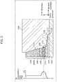
- FIG. 1 is a cross-sectional view illustrating a configuration of semiconductor device 100 according to the embodiment.
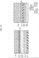
- FIG. 2 is an enlarged cross-sectional view illustrating a configuration of semiconductor device 100 in proximity to an ohmic electrode.
- FIG. 3 illustrates plan views and cross-sectional views of semiconductor device 100 after dry etch processing, after wet etch processing, and after formation of the ohmic electrode.
- semiconductor device 100 is a heterojunction field effect transistor (HFET)
- HFET heterojunction field effect transistor
- semiconductor device 100 includes substrate 101, buffer layer 102, channel layer 103, barrier layer 104, two-dimensional electron gas layer 105, recess 106, gate electrode 107, source electrode 108S, and drain electrode 108D.
- source electrode 108S and drain electrode 108D are also referred to as ohmic electrode 108.
- Substrate 101 is, for example, a substrate including Si.
- Substrate 101 is not limited to a substrate including Si, but may also be a substrate including sapphire, SiC, GaN, AIN, or the like.
- Buffer layer 102 is formed above substrate 101.
- Buffer layer 102 is, for example, a group III nitride semiconductor layer having a thickness of 2 ⁇ m and including a plurality of laminated structures each including AIN and AIGaN.
- Buffer layer 102 may alternatively include a single layer or multiple layers of group III nitride semiconductors such as GaN, AIGaN, AIN, InGaN, AlInGaN, etc.
- Channel layer 103 is formed above substrate 101.
- channel layer 103 is formed above buffer layer 102 in the +c-plane direction ( ⁇ 0001> direction), for example.
- Channel layer 103 is a group III nitride semiconductor layer in which Al is not included, and includes GaN having a thickness of 200 nm, for example.
- channel layer 103 may include a group III nitride semiconductor of not only GaN but also InGaN or the like, as long as channel layer 103 is a group III nitride semiconductor layer in which Al is not included.
- channel layer 103 may contain an n-type impurity.
- Barrier layer 104 is formed above channel layer 103.
- barrier layer 104 is formed above channel layer 103 in the +c-plane direction ( ⁇ 0001> direction), for example.
- Barrier layer 104 is a group III nitride semiconductor layer in which Al is included.
- the Al composition ratio distribution of barrier layer 104 in the first direction perpendicular to substrate 101 has a maximum point at first position 109.
- two-dimensional electron gas that is highly concentrated is generated on the channel layer 103 side of the hetero interface between barrier layer 104 and channel layer 103 laminated in the +c-plane direction ( ⁇ 0001> direction), and a channel of two-dimensional electron gas layer 105 is formed.
- Recess 106 is formed so as to remove the entirety of barrier layer 104 and a portion of channel layer 103 from the surface of the laminated semiconductor including channel layer 103 and barrier layer 104. In addition, recess 106 is formed such that the distance between first position 109 and the bottom position of recess 106 is 6 nm.
- recess 106 need only be formed so as to remove at least a portion of barrier layer 104 from the surface of the laminated semiconductor including channel layer 103 and barrier layer 104, and do not necessarily need to be limited to the example in which recess 106 is formed so as to remove the entirety of barrier layer 104 and a portion of channel layer 103.
- Gate electrode 107 is formed above barrier layer 104. Gate electrode 107 is in contact with barrier layer 104. More specifically, gate electrode 107 is Schottky bonded to barrier layer 104. Gate electrode 107 has, for example, a multilayer film structure including a Ni film and an Au film laminated in sequence.
- gate electrode 107 may be a single layer structure, or a multilayer film structure including Ti, TiN, Ta, TaN, Pt, Pd, Al, W, WN, WSi, Cu, etc. which are laminated in order.
- gate electrode 107 and barrier layer 104 need not necessarily be limited to the example in which gate electrode 107 is Schottky bonded to barrier layer 104, and may be in contact with each other by a PN junction, or gate electrode 107 and barrier layer 104 may form a metal-insulator-semiconductor (MIS) structure, a metal-oxide-semiconductor (MOS) structure, etc., for example.
- MIS metal-insulator-semiconductor
- MOS metal-oxide-semiconductor
- Ohmic electrode 108 is formed above substrate 101.
- Ohmic electrode 108 is, for example, a multilayer electrode film that has a laminated structure including a Ti film and an Al film laminated in order.
- ohmic electrode 108 is not limited to the combination of Ti and Al, but may be a single layer electrode film including a single metal such as Ti, Au, Ta, Al, Mo, Hf, Zr, Au, Cu, etc., or a multilayer electrode film including a combination of two or more of these metals.
- Ohmic electrode 108 is disposed in recess 106 and electrically connected to two-dimensional electron gas layer 105. More specifically, barrier layer 104 and channel layer 103 of a side surface of recess 106 react with ohmic electrode 108 as a result of heat treatment to form nitrogen holes and become n-type. In addition, the face of recess 106 at which barrier layer 104 and channel layer 103 are exposed is a semi-polar plane, which makes it easier to form nitrogen holes and to become n-type. In this manner, ohmic electrode 108 is in ohmic contact with two-dimensional electron gas layer 105.
- the semi-polar plane refers to a plane other than a plane in which atoms are regularly arranged in a GaN crystal.
- barrier layer 104 is a group III nitride semiconductor layer that includes, for example, Al diffusion layer 120 having a thickness of 1 nm, AIN layer 119 having a thickness of 1 nm, Al diffusion layer 120 having a thickness of 1 nm, and AIGaN layer 104A having a thickness of 20 nm and an Al composition ratio of 25%, which are laminated in stated order.
- Al diffusion layer 120 is formed on the channel layer 103 side and the AIGaN layer 104A side as a result of diffusion of Al from AIN layer 119 due to the heat generated when AIN layer 119 and barrier layer 104 are deposited.
- AIN layer 119 which is a spacer layer in barrier layer 104
- AIGaN layer 104A may contain In, and barrier layer 104 may contain an n-type impurity.
- recess 106 includes first inclined surface 110 having a maximum point of the Al composition ratio distribution at first position 109 in contact with ohmic electrode 108, second inclined surface 111 below first inclined surface 110, and third inclined surface 112. More specifically, as illustrated in column (b) of FIG. 3 , in the first direction, recess 106 includes: first inclined surface 110; second inclined surface 111 intersecting first inclined surface 110 at second position 115 in a cross-sectional view and first intersection line 114 in a plan view; and third inclined surface 112 intersecting second inclined surface 111 at third position 124 in the cross-sectional view and second intersection line 116 in the plan view.
- Third inclined surface 112 intersects the bottom surface of recess 106 at fourth position 126 which is an edge portion of the bottom surface of recess 106 in the cross-sectional view, and at third intersection line 125 in the plan view.
- the angle of second inclined surface 111 to the surface of substrate 101 is smaller than the angle of first inclined surface 110 to the surface of substrate 101, and second position 115 is lower than first position 109.
- the distance from first position 109 to second position 115 is, for example, 1 nm.
- first position 109 to second position 115 may be greater than 0.5 nm and less than or equal to 4 nm. As described above, it is possible to increase a contact area between ohmic electrode 108 and two-dimensional electron gas layer 105, by reducing the distance from first position 109 to second position 115.
- the angle of second inclined surface 111 to the surface of substrate 101 is smaller than the angle of third inclined surface 112 to the surface of substrate 101.
- the angle of third inclined surface 112 to the surface of substrate 101 is smaller than the angle of first inclined surface 110 to the surface of substrate 101.
- the angles of first inclined surface 110, second inclined surface 111, and third inclined surface 112 to the surface of substrate 101 are arranged such that, for example, the angle of first inclined surface 110 is 70 degrees, the angle of second inclined surface 111 is 2 degrees, and the angle of third inclined surface 112 is 45 degrees.
- the angle of second inclined surface 111 to the surface of substrate 101 may be less than or equal to 5 degrees. As described above, it is possible to increase the contact area between ohmic electrode 108 and two-dimensional electron gas layer 105, by reducing the angle of second inclined surface 111 to the surface of substrate 101.
- first intersection line 114 includes recess portions 117 on the first inclined surface 110 side in the second direction in which first inclined surface 110 and second inclined surface 111 are arranged.
- Recess portions 117 are irregularly arranged in the third direction that is an extending direction of first intersection line 114.
- Second position 115A in recess portions 117 is recessed toward the first inclined surface 110 side compared to second position 115 in other than recess portions 117, thereby increasing the area of second inclined surface 111. As a result, it is possible to further reduce the resistance of the ohmic contact.
- the angle of second inclined surface 111 to the surface of substrate 101 may be less than 90 degrees. As described above, it is possible to increase the contact area between ohmic electrode 108 and two-dimensional electron gas layer 105, by setting the angle of second inclined surface 111 to the surface of substrate 101 to less than 90 degrees.
- recess portions 117 may each include a curved portion in a plan view. In this case, it is possible to alleviate the electric field that concentrates at an edge of the ohmic electrode, by including a curved portion in each of recess portions 117. As a result, it is possible to inhibit destruction of the device.
- the depth of recess portions 117 in the second direction may be 10 nm to 40 nm.
- the width of each of recess portions 117 may be 100 nm to 500 nm in the third direction.
- recess portions 117 that are arranged may be spaced apart from each other with an interval of 100 nm to 600 nm in the third direction, with a pitch of 200 nm to 1100 nm.
- second position 115 is lower than first position 109, and thus it is possible to make barrier layer 104 on second inclined surface 111 significantly thin, compared to the conventional technique of PTL 1. Therefore, ohmic electrode 108 and two-dimensional electron gas layer 105 can be in ohmic contact with each other via second inclined surface 111, and thus it is possible to increase the contact area.
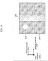
- FIG. 4 is an enlarged plan view illustrating a configuration of semiconductor device 100 in proximity to a gate electrode.
- the extending direction of gate electrode 107 in a plan view of substrate 101 may be in a ⁇ 11-20> direction of orientation 118 of a semiconductor crystal configuring channel layer 103. Since semiconductor device 100 has such a configuration as described above, it is possible to improve the temperature characteristics of Vth.
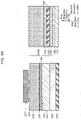
- the following describes a manufacturing method of semiconductor device 100 according to the present embodiment with reference to FIG. 5A through FIG. 5F , and FIG. 3 .
- FIG. 5A through FIG. 5F each illustrate a cross-sectional view and an enlarged cross-sectional view indicating a configuration of semiconductor device 100 during a manufacturing process.
- the diagram on the left side is a cross-sectional view illustrating the overall configuration of semiconductor device 100
- the diagram on the right side is an enlarged cross-sectional view illustrating the configuration in proximity to ohmic electrode 108.
- buffer layer 102 having a thickness of 2 ⁇ m and including a laminated structure of AIN and AIGaN, channel layer 103 having a thickness of 200 nm and including i-type GaN, AIN layer 119 having a thickness of 1 nm, and i-type AIGaN layer 104A having a thickness of 20 nm and an Al composition ratio of 25% are epitaxially grown in the +c-plane direction ( ⁇ 0001> direction) sequentially above substrate 101 including Si, using a metalorganic chemical vapor deposition (MOCVD).
- MOCVD metalorganic chemical vapor deposition
- Al diffusion layer 120 is formed on the channel layer 103 side and the AIGaN layer 104A side as a result of diffusion of Al from AIN layer 119 due to the heat generated when AIN layer 119 and AIGaN layer 104A are deposited.
- barrier layer 104 which includes Al diffusion layer 120, AIN layer 119, and AIGaN layer 104A, and has a maximum point of the Al composition ratio distribution at first position 109.
- the lower surface of Al diffusion layer 120 on the substrate 101 side becomes the hetero-interface.
- Two-dimensional electron gas that is highly concentrated is generated on the channel layer 103 side of the hetero interface between barrier layer 104 and channel layer 103, and a channel of two-dimensional electron gas layer 105 is formed.
- insulating layer 121 including SiN and having a thickness of 50 nm is deposited on barrier layer 104 using a plasma chemical vapor deposition (CVD) method, and then resist 127 is applied to the region where recess 106 is to be formed, followed by patterning of resist 127 using a lithography method.
- an opening is formed in insulating layer 121, using a wet etching method, such that barrier layer 104 is exposed.
- a side etch is provided in insulating layer 121 to form an opening, by causing the side surface of insulating layer 121 to be recessed inwardly relative to the side surface of resist 127 and positioned under resist 127.
- insulating layer 121 may be SiO 2 , SiON, or SiCN.
- barrier layer 104 and channel layer 103 are partially removed by performing etching processing with Cl 2 gas, using an inductively coupled plasma (ICP) dry etching device with resist 127 as a mask.
- ICP inductively coupled plasma
- fourth position 126 is formed at the edge portion of the bottom surface of the recess.
- fourth position 126 corresponds to third intersection line 125 as illustrated in column (a) of FIG. 3 .
- crystal defects are generated on the surface of barrier layer 104 and channel layer 103 exposed by the dry etch processing, and high resistance layer 122 is formed.
- the distance between first position 109 and the bottom position of recess 106 is 6 nm according to the present embodiment.
- the distance between first position 109 and the bottom position of recess 106 may be greater than or equal to 1 nm and less than or equal to 10 nm.
- the side surface of insulating layer 121 is caused to be recessed inwardly relative to the side surface of resist 127 during the wet etching, and thus is positioned under resist 127. As a result, the side surface of insulating layer 121 is protected by resist 127. For that reason, the top and side surfaces of insulating layer 121 are not subject to loss due to dry etching. Therefore, during the heat treatment to form an ohmic contact, it is possible to reduce the interdiffusion between ohmic electrode 108 and insulating layer 121.
- recess 106 was formed using resist 127 as a mask in the present embodiment, recess 106 may be formed using insulating layer 121 as a mask after removing resist 127.
- plasma processing by the ICP dry etching device is described according to the present embodiment.
- plasma processing by a capacitively coupled plasma (CCP) or an electron cyclotron resonance (ECR) dry etching device may be used.
- the etching processing using the ICP dry etching device is performed, for example, by introducing CL 2 gas at a gas flow rate of 10 sccm to 30 sccm, using Cl 2 as a gas feedstock.
- Cl 2 gas in addition to Cl 2 gas, SiH 4 as a material containing silicon (Si) and/or SiCl 4 , BCl 3 , or CCI as a material containing chlorine may be added.
- Ar (Argon) or He (Helium) that are inert gas may be introduced to dilute Cl 2 gas.
- the setting conditions for the etching processing are, for example, 0.5 Pa to 3 Pa for the pressure of an etching process atmosphere, 50 W to 200 W for the power applied to an upper electrode by the 13.56 MHz power supply, 5 W to 20 W for the power applied to a lower electrode by the 13.56 MHz power supply, and 0 degrees Celsius to 20 degrees Celsius for the temperature of the substrate.
- resist 127 is removed using a resist removal solution
- the polymer is removed using a polymer cleaning solution
- channel layer 103 and barrier layer 104 exposed to the side surface of recess 106 are subjected to wet etching using an alkaline chemical solution with a pH value of 10 to 14 and a temperature of greater than or equal to 65 degrees Celsius, only in a side-surface direction with barrier layer 104 being in high selectivity relative to channel layer 103.
- first inclined surface 110 including first position 109 and second inclined surface 111 are formed in barrier layer 104
- third inclined surface 112 is formed in channel layer 103.
- second position 115 at which first inclined surface 110 formed intersects second inclined surface 111 formed and third position 124 at which second inclined surface 111 formed intersects third inclined surface 112 formed are formed.
- Second position 115 and third position 124 in the cross-sectional view correspond to first intersection line 114 and second intersection line 116, respectively, in the plan view.
- second position 115 is located below first position 109.
- the angles of first inclined surface 110, second inclined surface 111, and third inclined surface 112 with respect to the surface of substrate 101 are formed such that the angle of first inclined surface 110 is 70 degrees, the angle of second inclined surface 111 is 2 degrees, and the angle of third inclined surface 112 is 45 degrees, for example.
- first inclined surface 110 and second inclined surface 111 since the wet etch processing removes at least a portion of barrier layer 104 to form first inclined surface 110 and second inclined surface 111, high resistance layer 122 on first inclined surface 110 and second inclined surface 111 is at least partially removed. Since at least a portion of the surface of barrier layer 104 where gate electrode 107 is formed is covered by insulating layer 121, it is possible to inhibit an increase of crystal defects caused by an alkaline chemical solution in barrier layer 104 under gate electrode 107.
- dislocations 123 are present in barrier layer 104.
- barrier layer 104 is etched with dislocations 123 as starting points, and a plurality of recess portions 117 each including a curve are irregularly formed in barrier layer 104.
- the angle of first inclined surface 110 to the surface of substrate 101 in recess portions 117 is less than 90 degrees, and the depth of recess portions 117 in the second direction is 10 nm to 40 nm.
- the width of recess portions 117 may be 100 nm to 500 nm in the third direction.
- first inclined surface 110, second inclined surface 111, and third inclined surface 112 are formed by etching barrier layer 104 only in the side-surface direction with barrier layer 104 being in high selectivity relative to channel layer 103, using an alkaline chemical solution will be described.
- the etching of AIGaN using an alkaline chemical solution involves crystal orientation dependency and is difficult to etch from the top surface, but can be done from the side surface.
- the polar plane includes Group III Al or Ga, and thus the etching rate significantly slows down.
- the side surface is a semi-polar plane, and thus can be etched at a certain rate.
- the alkaline chemical solution has a pH value of 10 to 14 and a temperature of greater than or equal to 65 degrees Celsius, GaN that contains no Al is not etched, and thus the etching rate gradually increases as the Al content of AIGaN increases.
- barrier layer 104 that contains Al without etching channel layer 103 that contains no Al, and AIN layer 119 that includes first position 109 that is a maximum point in the Al composition ratio distribution in barrier layer 104 is etched the most.
- first inclined surface 110, second inclined surface 111, and third inclined surface 112 are formed with high precision.
- second position 115 is located below first position 109.
- the angle of second inclined surface 111 to the surface of substrate 101 is smaller than the angle of first inclined surface 110 to the surface of substrate 101.
- the angle of second inclined surface 111 to the surface of the substrate is smaller than the angle of third inclined surface 112 to the surface of substrate 101.
- the angle of third inclined surface 112 to the surface of substrate 101 is smaller than the angle of first inclined surface 110 to the surface of substrate 101.
- the angle of first inclined surface 110 to the surface of substrate 101 is less than 90 degrees.
- it is better that the angle of second inclined surface 111 to the surface of the substrate is smaller than or equal to 5 degrees.
- barrier layer 104 and channel layer 103 on the surface of recess 106 may be made n-type by plasma processing including SiCl 4 gas.
- a portion of barrier layer 104 and a portion of channel layer 103 may be made n-type by ion implantation device in a predetermined region.
- etching processing using ammonium-hydrogen peroxide mixture is explained according to the present embodiment.
- etching processing using tetramethyl ammonium hydroxide (TMAH), kalium hydroxide (KOH), etc. may be performed.
- the pH value of the alkaline chemical solution may be 10 to 14, and the temperature of the chemical solution may be greater than or equal to 65 degrees Celsius. According to the above-described configuration, it is possible to etch barrier layer 104 only on the side surface with barrier layer 104 being in high selectivity relative to channel layer 103.
- a Ti film and an Al film are sequentially deposited by the sputtering method, and then the lithography method and the dry etching method are applied in sequence for patterning the laminated film of the Ti film and the Al film, thereby forming ohmic electrode 108 that has a predetermined shape on recess 106.
- ohmic electrode 108 that has a predetermined shape may be formed by using a lift-off method to sequentially deposit the Ti film and the Al film with a vapor-deposition technique instead of the sputtering method.
- ohmic electrode 108 is not limited to a combination of Ti and Al, but may be a single layer electrode film including a single metal such as Ti, Au, Ta, Al, Mo, Hf, Zr, Au, or Cu, or a multilayer electrode film including a combination of two or more of these metals.
- first inclined surface 110 to the surface of substrate 101 is less than 90 degrees, it is possible to implant metal atoms to second inclined surface 111 when ohmic electrode 108 is deposited by sputtering. As a result, it is possible to further reduce the resistance of the ohmic contact. In addition, when ohmic electrode 108 is deposited by sputtering, it is possible to deposit it with good coverage. As a result, it is possible to stably reduce the resistance of the ohmic contact.
- second inclined surface 111 is a semi-polar plane of the semiconductor crystal that constitutes barrier layer 104, which makes it easier to form nitrogen holes and to make it n-type.
- the temperature of the heat treatment is 500 degrees Celsius according to the present embodiment, the temperature of the heat treatment may be less than or equal to 500 degrees Celsius, or greater than or equal to 500 degrees Celsius and less than 1000 degrees Celsius.
- gate electrode 107 is formed above barrier layer 104 by patterning the laminated films of the Ni film and the Au film by applying the lithography method and the dry etching method in sequence after sequentially depositing the Ni film and the Au film by the sputtering method.
- gate electrode 107 that has a predetermined shape may be formed by using the lift-off method to sequentially deposit the Ni film and the Au film with a vapor-deposition technique instead of the sputtering method.
- the extending direction of gate electrode 107 in a plan view of substrate 101 may be in a ⁇ 11-20> direction of a semiconductor crystal configuring channel layer 103.
- second position 115 is lower than first position 109 at which the Al composition ratio distribution has a maximum point, and thus it is possible to make barrier layer 104 on second inclined surface 111 quite thin. Therefore, ohmic electrode 108 and two-dimensional electron gas layer 105 can be in ohmic contact with each other via second inclined surface 111, and thus it is possible to increase the contact area.
- second inclined surface 111 is formed by wet etching, high resistance layer 122 formed by dry etching is at least partially removed.
- the distance between two-dimensional electron gas layer 105 and ohmic electrode 108 is short and there is no resistance component, and thus it is possible to further reduce the resistance of the ohmic contact.
- FIG. 6 illustrates a cross-sectional transmission electron microscope (TEM) photograph showing the cross-section in proximity to the ohmic electrode in the configuration example illustrated in FIG. 2 .
- second position 115 is lower than first position 109 at which the Al composition ratio distribution has a maximum point, and the angles of first inclined surface 110, second inclined surface 111, and third inclined surface 112 to the surface of substrate 101 are 70 degrees, 2 degrees, and 45 degrees, respectively.
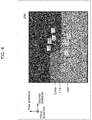
- FIG. 7 illustrates a scanning Electron microscope (SEM) photograph showing the plane of the recess portion after the wet etch processing in the configuration example illustrated in column (b) of FIG. 3 .
- SEM scanning Electron microscope
- the semiconductor device according to the present disclosure is useful for power switching devices, etc. for use in communication devices, inverters, and power supply circuits that require high-speed operation.
Landscapes
- Engineering & Computer Science (AREA)
- Microelectronics & Electronic Packaging (AREA)
- Power Engineering (AREA)
- Condensed Matter Physics & Semiconductors (AREA)
- General Physics & Mathematics (AREA)
- Physics & Mathematics (AREA)
- Computer Hardware Design (AREA)
- Ceramic Engineering (AREA)
- Manufacturing & Machinery (AREA)
- Chemical & Material Sciences (AREA)
- Crystallography & Structural Chemistry (AREA)
- Junction Field-Effect Transistors (AREA)
- Electrodes Of Semiconductors (AREA)
Abstract
Description
- The present disclosure relates to semiconductor devices, and particularly relates to a group III nitride semiconductor device using a group III nitride semiconductor. This is a patent application concerning the results of research commissioned by the Japanese government, etc. (a patent application subject to Article 17 of the Industrial Technology Enhancement Act in connection with a project for research and development related to basic technologies for the prevalence and deployment of 5G commissioned by the Ministry of Internal Affairs and Communications in the second year of Reiwa (2020)).
- The group III nitride semiconductor devices using the group III nitride semiconductors, especially GaN (gallium nitride) or AIGaN (aluminum gallium nitride), have high dielectric breakdown voltages due to the wide bandgap of the materials. In addition, with the group III nitride semiconductor devices, a hetero structure such as AlGaN/GaN can be easily formed.
- With the AlGaN/GaN hetero structure, due to the difference between piezoelectric polarization generated by the difference in lattice constants between the materials and the spontaneous polarization of AIGaN and GaN, a channel consisting of high-concentration electrons (hereinafter referred to as a "two-dimensional electron gas layer") on the GaN layer side of the AlGaN/GaN interface. The group III nitride semiconductor devices using the channels of the above-described two-dimensional electron gas layer have a relatively high electron saturation velocity, relatively high insulation resistance, and relatively high thermal conductivity, and thus are applied to high-frequency power devices.
- In order to enhance the characteristics of the above-described group III nitride semiconductor devices, the parasitic resistance components such as the contact (hereinafter referred to as an ohmic contact) between the ohmic electrode and the two-dimensional electron gas layer in the group III nitride semiconductor device and the resistance of the channel may be reduced as much as possible.
-
FIG. 8 is a cross-sectional view illustrating a configuration in proximity to an ohmic electrode in a group III nitride semiconductor device described in Patent Literature (PTL) 1. As illustrated inFIG. 8 , according toPTL 1,buffer layer 1102, GaN layer 1103A,AIN layer 1119, and AIGaN layer 1104A are formed in order abovesubstrate 1101, and two-dimensional electron gas layer 1105 resulting from the hetero structure ofAIN layer 1119 and GaN layer 1103A is provided on a GaN layer 1103A side.Ohmic electrode 1108 is formed onrecess 1106 where portions of AIGaN layer 1104A,AIN layer 1119, and GaN layer 1103A have been removed. It is described that the angle ofrecess 1106 intersecting the hetero interface betweenAIN layer 1119 and GaN layer 1103A to the surface ofsubstrate 1101 on the acute angle side is greater than 0 degrees and less than or equal to 56 degrees. According to the above-described configuration, with the semiconductor device described inPTL 1, two-dimensional electron gas layer 1105 andohmic electrode 1108 can be in contact with each other and the contact area can be increased, and thus it is possible to reduce the resistance of the ohmic contact. - [PTL 1]
Japanese Unexamined Patent Application Publication No. 2007-053185 - According to the method described in
PTL 1 above, the contact area between two-dimensional electron gas layer 1105 andohmic electrode 1108 is increased by reducing the angle ofrecess 1106 intersecting the hetero interface betweenAIN layer 1119 and GaN layer 1103A to the surface of thesubstrate 1101 on the acute angle side. However, the contact area is still insufficient. In addition,AIN layer 1119 is capable of improving the electron mobility and sheet carrier concentration of two-dimensional electron gas layer 1105, and thus is indispensable for enhancing the performance of the group III nitride semiconductor device. However, due to the large bandgap, there is a problem that contact from AIGaN layer 1104A that is an upper layer becomes significantly high resistance resulting fromAIN layer 1119 being a barrier. - Furthermore, since
recess 1106 is formed by dry etching,high resistance layer 1122 including a crystal defect is formed on the surface of AIGaN layer 1104A,AIN layer 1119, and GaN layer 1103A exposed byrecess 1106. For that reason, two-dimensional electron gas layer 1105 andohmic electrode 1108 are not in direct contact with each other, and are distant from each other by the width ofhigh resistance layer 1122. As a result, the resistance of the ohmic contact is increased. - As described above, with the conventional techniques, there is a problem that it is not possible to sufficiently reduce the resistance of the ohmic contact.
- The present disclosure has been conceived in view of the above-described problems, and has an object to provide a semiconductor device capable of reducing the resistance of the ohmic contact.
- A semiconductor device according to one aspect of the present disclosure includes: a substrate; a channel layer disposed above the substrate, the channel layer being a group III nitride not containing Al; a barrier layer disposed above the channel layer, the barrier layer being a group III nitride containing Al; a gate electrode joined to the barrier layer; a recess defined by removing at least a portion of the barrier layer from a surface of a laminated semiconductor including the channel layer and the barrier layer; and an ohmic electrode disposed in the recess, the ohmic electrode being in ohmic contact with a two-dimensional electron gas layer generated in the channel layer. In the semiconductor device, an Al composition ratio distribution of the barrier layer in a first direction perpendicular to a surface of the substrate has a maximum point at a first position, the semiconductor device includes, in the first direction: a first inclined surface of the barrier layer, the first inclined surface including the first position and being in contact with the ohmic electrode; and a second inclined surface of the barrier layer, the second inclined surface intersecting the first inclined surface at a first intersection line on a lower side of the first inclined surface and being in contact with the ohmic electrode, an angle of the second inclined surface to the surface of the substrate is smaller than an angle of the first inclined surface to the surface of the substrate, and a second position that is a position of the first intersection line in the first direction is lower than the first position.
- A manufacturing method of a semiconductor device according to one aspect of the present disclosure includes: forming a channel layer above a substrate, the channel layer being a group III nitride not containing Al; forming a barrier layer above the channel layer, the barrier layer being a group III nitride containing Al; performing dry etching to define a recess by removing at least a portion of the barrier layer from a surface of a laminated semiconductor including the channel layer and the barrier layer; performing wet etching using an alkaline chemical solution after the performing of the dry etching, the alkaline chemical solution having a pH value of 10 to 14 and a temperature of greater than or equal to 65 degrees Celsius; forming an ohmic electrode to fill the recess after the performing of the wet etching; and performing a heat treatment on the ohmic electrode.
- A manufacturing method of a semiconductor device according to one aspect of the present disclosure includes: forming a channel layer above a substrate, the channel layer being a group III nitride; forming a barrier layer above the channel layer, the barrier layer being the group III nitride and having a band gap larger than a band gap of the channel layer; forming an insulating layer above the barrier layer; forming a mask above the insulating layer, the mask being provided with an opening; forming a side etch by removing, using the mask, (i) an entirety of the insulating layer in a region exposed by the opening and (ii) a portion of the insulating layer to cause a side surface of the insulating layer to be recessed inwardly relative to a side surface of the mask; removing at least a portion of the barrier layer and the channel layer to define a recess, by dry etching using the mask; removing the mask; forming an ohmic electrode to cover the recess and a portion of the insulating layer; and performing a heat treatment on the ohmic electrode.
- A semiconductor device capable of reducing ohmic resistance is provided.
-
- [
FIG. 1 ]
FIG. 1 is a cross-sectional view illustrating a configuration of a semiconductor device according to an embodiment. - [
FIG. 2 ]
FIG. 2 is an enlarged cross-sectional view illustrating a configuration of the semiconductor device in proximity to an ohmic electrode according to the embodiment. - [
FIG. 3 ]
FIG. 3 illustrates plan views and cross-sectional views of the semiconductor device after dry etch processing, after wet etch processing, and after formation of the ohmic electrode, according to the embodiment. - [
FIG. 4 ]
FIG. 4 is an enlarged plan view illustrating a configuration of the semiconductor device in proximity to a gate electrode according to the embodiment. - [
FIG. 5A ]
FIG. 5A is a cross-sectional view and an enlarged cross-sectional view illustrating a configuration of the semiconductor device during a manufacturing process according to the embodiment. - [
FIG. 5B ]
FIG. 5B is a cross-sectional view and an enlarged cross-sectional view illustrating a configuration of the semiconductor device during the manufacturing process according to the embodiment. - [
FIG. 5C ]
FIG. 5C is a cross-sectional view and an enlarged cross-sectional view illustrating a configuration of the semiconductor device during the manufacturing process according to the embodiment. - [
FIG. 5D ]
FIG. 5D is a cross-sectional view and an enlarged cross-sectional view illustrating a configuration of the semiconductor device during the manufacturing process according to the embodiment. - [
FIG. 5E ]
FIG. 5E is a cross-sectional view and an enlarged cross-sectional view illustrating a configuration of the semiconductor device during the manufacturing process according to the embodiment. - [
FIG. 5F ]
FIG. 5F is a cross-sectional view and an enlarged cross-sectional view illustrating a configuration of the semiconductor device during the manufacturing process according to the embodiment. - [
FIG. 6 ]
FIG. 6 is a transmission electron microscope (TEM) diagram illustrating a cross-section of the ohmic electrode in the semiconductor device according to the embodiment. - [
FIG. 7 ]
FIG. 7 is a scanning Electron microscope (SEM) diagram illustrating a planar surface of a recess after the wet etch processing in the semiconductor device according to the embodiment - [
FIG. 8 ]
FIG. 8 is an enlarged cross-sectional view illustrating a configuration of a conventional semiconductor device in proximity to an ohmic electrode. - The inventors have conducted a series of diligent investigation and experiments in order to provide a semiconductor device capable of reducing the resistance of an ohmic contact. As a result, the inventors have arrived at the following semiconductor device, etc.
- A semiconductor device according to one aspect of the present disclosure includes: a substrate; a channel layer disposed above the substrate, the channel layer being a group III nitride not containing Al; a barrier layer disposed above the channel layer, the barrier layer being a group III nitride containing Al; a gate electrode joined to the barrier layer; a recess defined by removing at least a portion of the barrier layer from a surface of a laminated semiconductor including the channel layer and the barrier layer; and an ohmic electrode disposed in the recess, the ohmic electrode being in ohmic contact with a two-dimensional electron gas layer generated in the channel layer. In the semiconductor device, an Al composition ratio distribution of the barrier layer in a first direction perpendicular to a surface of the substrate has a maximum point at a first position, the semiconductor device includes, in the first direction: a first inclined surface of the barrier layer, the first inclined surface including the first position and being in contact with the ohmic electrode; and a second inclined surface of the barrier layer, the second inclined surface intersecting the first inclined surface at a first intersection line on a lower side of the first inclined surface and being in contact with the ohmic electrode, an angle of the second inclined surface to the surface of the substrate is smaller than an angle of the first inclined surface to the surface of the substrate, and a second position that is a position of the first intersection line in the first direction is lower than the first position.
- According to the above-described semiconductor device, it is possible to make the barrier layer on the second inclined surface significantly thin. Therefore, the ohmic electrode and the two-dimensional electron gas layer can be in ohmic contact with each other via the second inclined surface, and thus it is possible to increase the contact area. In addition, it is possible to increase the contact area by reducing the angle of the second inclined surface to the surface of the substrate. In addition, since the second inclined surface is formed by wet etching, the high resistance layer formed by dry etching is at least partially removed. As a result, at the second inclined surface where the contacting area is increased, the distance between the two-dimensional electron gas layer and the ohmic electrode is short and there is no resistance component, and thus it is possible to reduce the resistance of an ohmic contact.
- In addition, a distance between the first position and the second position may be greater than 0.5 nm and less than or equal to 4 nm.
- According to the above-described configuration, the distance between the first position and the second position is made small, and thus the angle of the second inclined surface to the surface of the substrate is made small. As a result, the area of the second inclined surface can further be increased, and thus it is possible to further reduce the resistance of the ohmic contact.
- In addition, in a plan view of the substrate, in a plan view of the substrate: the first intersection line may include three or more recess portions each being recessed toward a first inclined surface side in a second direction in which the first inclined surface and the second inclined surface are arranged; and the three or more recess portions may be irregularly arranged in a third direction that is an extending direction of the first intersection line.
- According to the above-described configuration, the area of the second inclined surface can further be increased, and thus it is possible to further reduce the resistance of the ohmic contact.
- A semiconductor device according to one aspect of the present disclosure includes: a substrate; a channel layer disposed above the substrate, the channel layer being a group III nitride not containing Al; a barrier layer disposed above the channel layer, the barrier layer being a group III nitride containing Al; a gate electrode joined to the barrier layer; a recess defined by removing at least a portion of the barrier layer from a surface of a laminated semiconductor including the channel layer and the barrier layer; and an ohmic electrode disposed in the recess, the ohmic electrode being in ohmic contact with a two-dimensional electron gas layer generated in the channel layer. In the semiconductor device, an Al composition ratio distribution of the barrier layer in a first direction perpendicular to a surface of the substrate has a maximum point at a first position, the semiconductor device includes, in the first direction: a first inclined surface of the barrier layer, the first inclined surface including the first position and being in contact with the ohmic electrode; and a second inclined surface of the barrier layer, the second inclined surface intersecting the first inclined surface at a first intersection line on a lower side of the first inclined surface and being in contact with the ohmic electrode, and in a plan view of the substrate: the first intersection line includes three or more recess portions each being recessed toward a first inclined surface side in a second direction in which the first inclined surface and the second inclined surface are arranged; and the three or more recess portions are irregularly arranged in a third direction that is an extending direction of the first intersection line.
- With the above-described semiconductor device, it is possible to increase the area of the second inclined surface, by forming the recess portion. As a result, it is possible to reduce the resistance of the ohmic contact. In addition, since the second inclined surface is formed by wet etching, the high resistance layer formed by dry etching is at least partially removed. As a result, it is possible to reduce the resistance of the ohmic contact, as well as reducing the distance between the two-dimensional electron gas layer and the ohmic electrode.
- In addition, in each of the three or more recess portions, an angle of the second inclined surface to the surface of the substrate may be less than 90 degrees.
- According to the above-described configuration, the area of the second inclined surface in the recess portion can further be increased, and thus it is possible to further reduce the resistance of the ohmic contact.
- In addition, in each of the three or more recess portions, the first intersection line may include a curve.
- According to the above-described configuration, since the first intersection line includes a curve in the recess portion, it is possible to alleviate electric field concentration in the end portion of the ohmic electrode in the recess portion.
- In addition, each of the three or more recess portions may have a depth greater than or equal to 10 nm and less than or equal to 40 nm in the second direction.
- In addition, the barrier layer may include an AIN layer, and the first position may be located within a range defined by a thickness of the AIN layer in the first direction.
- In addition, an Al composition ratio of the barrier layer at the first position may be greater than or equal to 90%.
- In addition, in the first direction, a distance between the first position and a bottom position of the barrier layer may be less than or equal to 10% of a thickness of the barrier layer.
- In addition, a third inclined surface of the channel layer, the third inclined surface intersecting the second inclined surface at a second intersection line on a lower side of the second inclined surface, and being in contact with the ohmic electrode may be included. In the semiconductor device, the angle of the second inclined surface to the surface of the substrate may be smaller than an angle of the third inclined surface to the surface of the substrate.
- In addition, a third inclined surface of the channel layer, the third inclined surface intersecting the second inclined surface at a second intersection line on a lower side of the second inclined surface, and being in contact with the ohmic electrode may be included. In the semiconductor device, an angle of the third inclined surface to the surface of the substrate may be smaller than the angle of the first inclined surface to the surface of the substrate.
- According to the above-described configuration, since the second inclined surface is formed by wet etching, the angle of the second inclined surface to the surface of the substrate is made small. As a result, the area of the second inclined surface can further be increased, and thus it is possible to further reduce the resistance of the ohmic contact.
- In addition, the angle of the first inclined surface to the surface of the substrate may be less than 90 degrees.
- According to the above-described configuration, it is possible to implant metal atoms to the second inclined surface when an ohmic electrode is deposited by sputtering. As a result, it is possible to further reduce the resistance of the ohmic contact.
- In addition, the second inclined surface may be a semi-polar plane of a semiconductor crystal configuring the barrier layer.
- According to the above-described configuration, the second inclined surface is a semi-polar plane of the semiconductor crystal configuring the barrier layer, which facilitates formation of nitrogen holes by heat treatment when forming the ohmic electrode, and making it n-type. As a result, it is possible to further reduce the resistance of the ohmic contact.
- In addition, the angle of the second inclined surface to the surface of the substrate may be less than or equal to 5 degrees.
- According to the above-described configuration, the area of the second inclined surface can further be increased, and thus it is possible to further reduce the resistance of the ohmic contact.
- In addition, in the first direction, a distance between the first position and a bottom position of the recess may be greater than or equal to 1 nm and less than or equal to 10 nm.
- According to the above-described configuration, the distance between the first position and the bottom surface of the recess is made relatively small, and thus it is possible to reduce the time period of dry etching when forming the recess. It is thus possible to reduce the amount of formation of the high resistance layer that is formed on the side surface of the recess, thereby enabling an increase in the resistance value to be inhibited. As a result, it is possible to further reduce the resistance of the ohmic contact.
- In addition, a <0001> direction of a semiconductor crystal configuring the channel layer may be the first direction.
- According to the above-described configuration, the sheet carrier concentration of the two-dimensional electron gas layer can be increased, and thus it is possible to further reduce the resistance of the ohmic contact.
- In addition, an extending direction of the gate electrode in a plan view of the substrate may be a <11-20> direction of a semiconductor crystal configuring the channel layer.
- According to the above-described configuration, it is possible to enhance the temperature characteristics of Vth.
- A manufacturing method of a semiconductor device according to one aspect of the present disclosure includes: forming a channel layer above a substrate, the channel layer being a group III nitride not containing Al; forming a barrier layer above the channel layer, the barrier layer being a group III nitride containing Al; performing dry etching to define a recess by removing at least a portion of the barrier layer from a surface of a laminated semiconductor including the channel layer and the barrier layer; performing wet etching using an alkaline chemical solution after the performing of the dry etching, the alkaline chemical solution having a pH value of 10 to 14 and a temperature of greater than or equal to 65 degrees Celsius; forming an ohmic electrode to fill the recess after the performing of the wet etching; and performing a heat treatment on the ohmic electrode.
- According to the above-described manufacturing method of the semiconductor device, the second position that is the position of the first intersection line is lower than the first position that is the maximum point of the Al composition ratio distribution in the first direction, and thus it is possible to make the barrier layer on the second inclined surface significantly thin. Therefore, the ohmic electrode and the two-dimensional electron gas layer can be in ohmic contact with each other via the second inclined surface, and thus it is possible to increase the contact area. In addition, since the second inclined surface is formed by wet etching, the high resistance layer formed by dry etching is at least partially removed. As a result, at the second inclined surface where the contacting area is increased, the distance between the two-dimensional electron gas layer and the ohmic electrode is short and there is no resistance component, and thus it is possible to reduce the resistance of the ohmic contact.
- In addition, in a plan view of the substrate, the first intersection line is capable of including a recess portion on the first inclined surface side in the second direction in which the first inclined surface and the second inclined surface are arranged. In the case where three or more recess portions are included, the three or more recess portions are irregularly arranged in the third direction that is an extending direction of the first intersection line. As a result, the area of the second inclined surface can further be increased, and thus it is possible to further reduce the resistance of the ohmic contact.
- A manufacturing method of a semiconductor device according to one aspect of the present disclosure includes: forming a channel layer above a substrate, the channel layer being a group III nitride; forming a barrier layer above the channel layer, the barrier layer being the group III nitride and having a band gap larger than a band gap of the channel layer; forming an insulating layer above the barrier layer; forming a mask above the insulating layer, the mask being provided with an opening; forming a side etch by removing, using the mask, (i) an entirety of the insulating layer in a region exposed by the opening and (ii) a portion of the insulating layer to cause a side surface of the insulating layer to be recessed inwardly relative to a side surface of the mask; removing at least a portion of the barrier layer and the channel layer to define a recess, by dry etching using the mask; removing the mask; forming an ohmic electrode to cover the recess and a portion of the insulating layer; and performing a heat treatment on the ohmic electrode.
- Hereinafter, a semiconductor device according to an aspect of the present disclosure will be described with reference to the drawings. It should be noted that each of the exemplary embodiments described below shows a specific example of the present disclosure. The numerical values, shapes, elements, the arrangement and connection of the elements, steps (processes), and the processing order of the steps, for instance, described in the following embodiment are mere examples, and thus are not intended to limit the scope of the present disclosure. The drawings are schematic diagrams and do not necessarily give strict illustration. Throughout the drawings, the same numeral is given to substantially the same element, and redundant description is omitted or simplified.
- First, a semiconductor device according to an embodiment will be described with reference to
FIG. 1 ,FIG. 2 , andFIG. 3 . -
FIG. 1 is a cross-sectional view illustrating a configuration ofsemiconductor device 100 according to the embodiment.FIG. 2 is an enlarged cross-sectional view illustrating a configuration ofsemiconductor device 100 in proximity to an ohmic electrode.FIG. 3 illustrates plan views and cross-sectional views ofsemiconductor device 100 after dry etch processing, after wet etch processing, and after formation of the ohmic electrode. - In the present embodiment, the case where
semiconductor device 100 is a heterojunction field effect transistor (HFET) will be described. - As illustrated in
FIG. 1 ,semiconductor device 100 includessubstrate 101,buffer layer 102,channel layer 103,barrier layer 104, two-dimensionalelectron gas layer 105,recess 106,gate electrode 107,source electrode 108S, anddrain electrode 108D. Here, when there is no need to distinguish betweensource electrode 108S anddrain electrode 108D in the description,source electrode 108S anddrain electrode 108D are also referred to asohmic electrode 108. -
Substrate 101 is, for example, a substrate including Si.Substrate 101 is not limited to a substrate including Si, but may also be a substrate including sapphire, SiC, GaN, AIN, or the like. -
Buffer layer 102 is formed abovesubstrate 101.Buffer layer 102 is, for example, a group III nitride semiconductor layer having a thickness of 2 µm and including a plurality of laminated structures each including AIN and AIGaN.Buffer layer 102 may alternatively include a single layer or multiple layers of group III nitride semiconductors such as GaN, AIGaN, AIN, InGaN, AlInGaN, etc. -
Channel layer 103 is formed abovesubstrate 101. According to the present embodiment,channel layer 103 is formed abovebuffer layer 102 in the +c-plane direction (<0001> direction), for example.Channel layer 103 is a group III nitride semiconductor layer in which Al is not included, and includes GaN having a thickness of 200 nm, for example. - It should be noted that
channel layer 103 may include a group III nitride semiconductor of not only GaN but also InGaN or the like, as long aschannel layer 103 is a group III nitride semiconductor layer in which Al is not included. In addition,channel layer 103 may contain an n-type impurity. -
Barrier layer 104 is formed abovechannel layer 103. According to the present embodiment,barrier layer 104 is formed abovechannel layer 103 in the +c-plane direction (<0001> direction), for example.Barrier layer 104 is a group III nitride semiconductor layer in which Al is included. The Al composition ratio distribution ofbarrier layer 104 in the first direction perpendicular tosubstrate 101 has a maximum point atfirst position 109. - According to the present embodiment, two-dimensional electron gas that is highly concentrated is generated on the
channel layer 103 side of the hetero interface betweenbarrier layer 104 andchannel layer 103 laminated in the +c-plane direction (<0001> direction), and a channel of two-dimensionalelectron gas layer 105 is formed. - It should be noted that a cap layer that includes GaN and has a thickness of approximately 1 nm to 2 nm, for example, may be provided above
barrier layer 104 as a cap layer. -
Recess 106 is formed so as to remove the entirety ofbarrier layer 104 and a portion ofchannel layer 103 from the surface of the laminated semiconductor includingchannel layer 103 andbarrier layer 104. In addition,recess 106 is formed such that the distance betweenfirst position 109 and the bottom position ofrecess 106 is 6 nm. - It should be noted that
recess 106 need only be formed so as to remove at least a portion ofbarrier layer 104 from the surface of the laminated semiconductor includingchannel layer 103 andbarrier layer 104, and do not necessarily need to be limited to the example in whichrecess 106 is formed so as to remove the entirety ofbarrier layer 104 and a portion ofchannel layer 103. -
Gate electrode 107 is formed abovebarrier layer 104.Gate electrode 107 is in contact withbarrier layer 104. More specifically,gate electrode 107 is Schottky bonded tobarrier layer 104.Gate electrode 107 has, for example, a multilayer film structure including a Ni film and an Au film laminated in sequence. - It should be noted that
gate electrode 107 may be a single layer structure, or a multilayer film structure including Ti, TiN, Ta, TaN, Pt, Pd, Al, W, WN, WSi, Cu, etc. which are laminated in order. In addition,gate electrode 107 andbarrier layer 104 need not necessarily be limited to the example in whichgate electrode 107 is Schottky bonded tobarrier layer 104, and may be in contact with each other by a PN junction, orgate electrode 107 andbarrier layer 104 may form a metal-insulator-semiconductor (MIS) structure, a metal-oxide-semiconductor (MOS) structure, etc., for example. -
Ohmic electrode 108 is formed abovesubstrate 101.Ohmic electrode 108 is, for example, a multilayer electrode film that has a laminated structure including a Ti film and an Al film laminated in order. - It should be noted that
ohmic electrode 108 is not limited to the combination of Ti and Al, but may be a single layer electrode film including a single metal such as Ti, Au, Ta, Al, Mo, Hf, Zr, Au, Cu, etc., or a multilayer electrode film including a combination of two or more of these metals. -
Ohmic electrode 108 is disposed inrecess 106 and electrically connected to two-dimensionalelectron gas layer 105. More specifically,barrier layer 104 andchannel layer 103 of a side surface ofrecess 106 react withohmic electrode 108 as a result of heat treatment to form nitrogen holes and become n-type. In addition, the face ofrecess 106 at whichbarrier layer 104 andchannel layer 103 are exposed is a semi-polar plane, which makes it easier to form nitrogen holes and to become n-type. In this manner,ohmic electrode 108 is in ohmic contact with two-dimensionalelectron gas layer 105. Here, the semi-polar plane refers to a plane other than a plane in which atoms are regularly arranged in a GaN crystal. - Next, with reference to
FIG. 2 , the configuration ofsemiconductor device 100 in proximity toohmic electrode 108 will be described in more detail. - As illustrated in
FIG. 2 ,barrier layer 104 is a group III nitride semiconductor layer that includes, for example,Al diffusion layer 120 having a thickness of 1 nm,AIN layer 119 having a thickness of 1 nm,Al diffusion layer 120 having a thickness of 1 nm, andAIGaN layer 104A having a thickness of 20 nm and an Al composition ratio of 25%, which are laminated in stated order.Al diffusion layer 120 is formed on thechannel layer 103 side and theAIGaN layer 104A side as a result of diffusion of Al fromAIN layer 119 due to the heat generated whenAIN layer 119 andbarrier layer 104 are deposited. - It should be noted that, although the case where there is
AIN layer 119 which is a spacer layer inbarrier layer 104 has been described in the present embodiment, there may be noAIN layer 119. It should be noted thatAIGaN layer 104A may contain In, andbarrier layer 104 may contain an n-type impurity. - In addition,
recess 106 includes firstinclined surface 110 having a maximum point of the Al composition ratio distribution atfirst position 109 in contact withohmic electrode 108, secondinclined surface 111 below firstinclined surface 110, and thirdinclined surface 112. More specifically, as illustrated in column (b) ofFIG. 3 , in the first direction,recess 106 includes: firstinclined surface 110; secondinclined surface 111 intersecting firstinclined surface 110 atsecond position 115 in a cross-sectional view andfirst intersection line 114 in a plan view; and thirdinclined surface 112 intersecting secondinclined surface 111 atthird position 124 in the cross-sectional view andsecond intersection line 116 in the plan view. Thirdinclined surface 112 intersects the bottom surface ofrecess 106 atfourth position 126 which is an edge portion of the bottom surface ofrecess 106 in the cross-sectional view, and atthird intersection line 125 in the plan view. In addition, the angle of secondinclined surface 111 to the surface ofsubstrate 101 is smaller than the angle of firstinclined surface 110 to the surface ofsubstrate 101, andsecond position 115 is lower thanfirst position 109. - In the present embodiment, the distance from
first position 109 tosecond position 115 is, for example, 1 nm. - It should be noted that the distance from
first position 109 tosecond position 115 may be greater than 0.5 nm and less than or equal to 4 nm. As described above, it is possible to increase a contact area betweenohmic electrode 108 and two-dimensionalelectron gas layer 105, by reducing the distance fromfirst position 109 tosecond position 115. - In addition, the angle of second
inclined surface 111 to the surface ofsubstrate 101 is smaller than the angle of thirdinclined surface 112 to the surface ofsubstrate 101. In addition, the angle of thirdinclined surface 112 to the surface ofsubstrate 101 is smaller than the angle of firstinclined surface 110 to the surface ofsubstrate 101. According to the present embodiment, the angles of firstinclined surface 110, secondinclined surface 111, and thirdinclined surface 112 to the surface ofsubstrate 101 are arranged such that, for example, the angle of firstinclined surface 110 is 70 degrees, the angle of secondinclined surface 111 is 2 degrees, and the angle of thirdinclined surface 112 is 45 degrees. - It should be noted that the angle of second
inclined surface 111 to the surface ofsubstrate 101 may be less than or equal to 5 degrees. As described above, it is possible to increase the contact area betweenohmic electrode 108 and two-dimensionalelectron gas layer 105, by reducing the angle of secondinclined surface 111 to the surface ofsubstrate 101. - As illustrated in column (b) of
FIG. 3 ,first intersection line 114 includesrecess portions 117 on the firstinclined surface 110 side in the second direction in which first inclinedsurface 110 and secondinclined surface 111 are arranged.Recess portions 117 are irregularly arranged in the third direction that is an extending direction offirst intersection line 114.Second position 115A inrecess portions 117 is recessed toward the firstinclined surface 110 side compared tosecond position 115 in other thanrecess portions 117, thereby increasing the area of secondinclined surface 111. As a result, it is possible to further reduce the resistance of the ohmic contact. - It should be noted that, in
recess portions 117, the angle of secondinclined surface 111 to the surface ofsubstrate 101 may be less than 90 degrees. As described above, it is possible to increase the contact area betweenohmic electrode 108 and two-dimensionalelectron gas layer 105, by setting the angle of secondinclined surface 111 to the surface ofsubstrate 101 to less than 90 degrees. - In addition,
recess portions 117 may each include a curved portion in a plan view. In this case, it is possible to alleviate the electric field that concentrates at an edge of the ohmic electrode, by including a curved portion in each ofrecess portions 117. As a result, it is possible to inhibit destruction of the device. - The depth of
recess portions 117 in the second direction may be 10 nm to 40 nm. The width of each ofrecess portions 117 may be 100 nm to 500 nm in the third direction. In addition,recess portions 117 that are arranged may be spaced apart from each other with an interval of 100 nm to 600 nm in the third direction, with a pitch of 200 nm to 1100 nm. - As a result of
semiconductor device 100 having the above-described configuration,second position 115 is lower thanfirst position 109, and thus it is possible to makebarrier layer 104 on secondinclined surface 111 significantly thin, compared to the conventional technique ofPTL 1. Therefore,ohmic electrode 108 and two-dimensionalelectron gas layer 105 can be in ohmic contact with each other via secondinclined surface 111, and thus it is possible to increase the contact area. -
FIG. 4 is an enlarged plan view illustrating a configuration ofsemiconductor device 100 in proximity to a gate electrode. - As illustrated in
FIG. 4 , the extending direction ofgate electrode 107 in a plan view ofsubstrate 101 may be in a <11-20> direction oforientation 118 of a semiconductor crystal configuringchannel layer 103. Sincesemiconductor device 100 has such a configuration as described above, it is possible to improve the temperature characteristics of Vth. - The following describes a manufacturing method of
semiconductor device 100 according to the present embodiment with reference toFIG. 5A through FIG. 5F , andFIG. 3 . -
FIG. 5A through FIG. 5F each illustrate a cross-sectional view and an enlarged cross-sectional view indicating a configuration ofsemiconductor device 100 during a manufacturing process. InFIG. 5A to FIG. 5F , the diagram on the left side is a cross-sectional view illustrating the overall configuration ofsemiconductor device 100, and the diagram on the right side is an enlarged cross-sectional view illustrating the configuration in proximity toohmic electrode 108. - First, as illustrated in
FIG. 5A ,buffer layer 102 having a thickness of 2 µm and including a laminated structure of AIN and AIGaN,channel layer 103 having a thickness of 200 nm and including i-type GaN,AIN layer 119 having a thickness of 1 nm, and i-type AIGaN layer 104A having a thickness of 20 nm and an Al composition ratio of 25% are epitaxially grown in the +c-plane direction (<0001> direction) sequentially abovesubstrate 101 including Si, using a metalorganic chemical vapor deposition (MOCVD). At this time,Al diffusion layer 120 is formed on thechannel layer 103 side and theAIGaN layer 104A side as a result of diffusion of Al fromAIN layer 119 due to the heat generated whenAIN layer 119 andAIGaN layer 104A are deposited. In this manner,barrier layer 104 which includesAl diffusion layer 120,AIN layer 119, andAIGaN layer 104A, and has a maximum point of the Al composition ratio distribution atfirst position 109. The lower surface ofAl diffusion layer 120 on thesubstrate 101 side becomes the hetero-interface. - Two-dimensional electron gas that is highly concentrated is generated on the
channel layer 103 side of the hetero interface betweenbarrier layer 104 andchannel layer 103, and a channel of two-dimensionalelectron gas layer 105 is formed. - Next, as illustrated in
FIG. 5B , insulatinglayer 121 including SiN and having a thickness of 50 nm is deposited onbarrier layer 104 using a plasma chemical vapor deposition (CVD) method, and then resist 127 is applied to the region whererecess 106 is to be formed, followed by patterning of resist 127 using a lithography method. Next, an opening is formed in insulatinglayer 121, using a wet etching method, such thatbarrier layer 104 is exposed. In addition, using the wet etching method, a side etch is provided in insulatinglayer 121 to form an opening, by causing the side surface of insulatinglayer 121 to be recessed inwardly relative to the side surface of resist 127 and positioned under resist 127. It should be noted that, although the wet etching method is used according to the present embodiment, a chemical dry etching method may be used to define an opening in insulatinglayer 121. In addition, insulatinglayer 121 may be SiO2, SiON, or SiCN. - Next, as illustrated in
FIG. 5C ,barrier layer 104 andchannel layer 103 are partially removed by performing etching processing with Cl2 gas, using an inductively coupled plasma (ICP) dry etching device with resist 127 as a mask. In this manner,fourth position 126 is formed at the edge portion of the bottom surface of the recess. In a plan view,fourth position 126 corresponds tothird intersection line 125 as illustrated in column (a) ofFIG. 3 . At this time, crystal defects are generated on the surface ofbarrier layer 104 andchannel layer 103 exposed by the dry etch processing, andhigh resistance layer 122 is formed. In the first direction, the distance betweenfirst position 109 and the bottom position ofrecess 106 is 6 nm according to the present embodiment. In this way, it is possible to inhibit an increase in resistance ofhigh resistance layer 122 by reducing the dry etching time during the formation ofrecess 106. In addition, in the first direction, the distance betweenfirst position 109 and the bottom position ofrecess 106 may be greater than or equal to 1 nm and less than or equal to 10 nm. The side surface of insulatinglayer 121 is caused to be recessed inwardly relative to the side surface of resist 127 during the wet etching, and thus is positioned under resist 127. As a result, the side surface of insulatinglayer 121 is protected by resist 127. For that reason, the top and side surfaces of insulatinglayer 121 are not subject to loss due to dry etching. Therefore, during the heat treatment to form an ohmic contact, it is possible to reduce the interdiffusion betweenohmic electrode 108 and insulatinglayer 121. - It should be noted that, although
recess 106 was formed using resist 127 as a mask in the present embodiment,recess 106 may be formed using insulatinglayer 121 as a mask after removing resist 127. - As a specific example of the dry etch processing, for example, plasma processing by the ICP dry etching device is described according to the present embodiment. However, plasma processing by a capacitively coupled plasma (CCP) or an electron cyclotron resonance (ECR) dry etching device may be used.
- The etching processing using the ICP dry etching device is performed, for example, by introducing CL2 gas at a gas flow rate of 10 sccm to 30 sccm, using Cl2 as a gas feedstock. At this time, in addition to Cl2 gas, SiH4 as a material containing silicon (Si) and/or SiCl4, BCl3, or CCI as a material containing chlorine may be added. In addition, Ar (Argon) or He (Helium) that are inert gas may be introduced to dilute Cl2 gas. The setting conditions for the etching processing are, for example, 0.5 Pa to 3 Pa for the pressure of an etching process atmosphere, 50 W to 200 W for the power applied to an upper electrode by the 13.56 MHz power supply, 5 W to 20 W for the power applied to a lower electrode by the 13.56 MHz power supply, and 0 degrees Celsius to 20 degrees Celsius for the temperature of the substrate.
- Next, as illustrated in
FIG. 5D , resist 127 is removed using a resist removal solution, the polymer is removed using a polymer cleaning solution, and thenchannel layer 103 andbarrier layer 104 exposed to the side surface ofrecess 106 are subjected to wet etching using an alkaline chemical solution with a pH value of 10 to 14 and a temperature of greater than or equal to 65 degrees Celsius, only in a side-surface direction withbarrier layer 104 being in high selectivity relative tochannel layer 103. In this manner, in cross-sectional view, firstinclined surface 110 includingfirst position 109 and secondinclined surface 111 are formed inbarrier layer 104, and thirdinclined surface 112 is formed inchannel layer 103. As a result, as illustrated in column (b) ofFIG. 3 , in cross-sectional view,second position 115 at which first inclinedsurface 110 formed intersects secondinclined surface 111 formed andthird position 124 at which second inclinedsurface 111 formed intersects thirdinclined surface 112 formed are formed.Second position 115 andthird position 124 in the cross-sectional view correspond tofirst intersection line 114 andsecond intersection line 116, respectively, in the plan view. At this time,second position 115 is located belowfirst position 109. The angles of firstinclined surface 110, secondinclined surface 111, and thirdinclined surface 112 with respect to the surface ofsubstrate 101 are formed such that the angle of firstinclined surface 110 is 70 degrees, the angle of secondinclined surface 111 is 2 degrees, and the angle of thirdinclined surface 112 is 45 degrees, for example. - In addition, since the wet etch processing removes at least a portion of
barrier layer 104 to form firstinclined surface 110 and secondinclined surface 111,high resistance layer 122 on firstinclined surface 110 and secondinclined surface 111 is at least partially removed. Since at least a portion of the surface ofbarrier layer 104 wheregate electrode 107 is formed is covered by insulatinglayer 121, it is possible to inhibit an increase of crystal defects caused by an alkaline chemical solution inbarrier layer 104 undergate electrode 107. - In addition, as illustrated in column (a) of
FIG. 3 ,dislocations 123 are present inbarrier layer 104. As illustrated in column (b) ofFIG. 3 , during the wet etch processing,barrier layer 104 is etched withdislocations 123 as starting points, and a plurality ofrecess portions 117 each including a curve are irregularly formed inbarrier layer 104. The angle of firstinclined surface 110 to the surface ofsubstrate 101 inrecess portions 117 is less than 90 degrees, and the depth ofrecess portions 117 in the second direction is 10 nm to 40 nm. It should be noted that the width ofrecess portions 117 may be 100 nm to 500 nm in the third direction. In addition, there may be three ormore recess portions 117 that are arranged so as to be spaced apart from each other with an interval of 100 nm to 600 nm in the third direction, with a pitch of 200 nm to 1100 nm. - Here, the reason why first inclined
surface 110, secondinclined surface 111, and thirdinclined surface 112 are formed byetching barrier layer 104 only in the side-surface direction withbarrier layer 104 being in high selectivity relative tochannel layer 103, using an alkaline chemical solution will be described. The etching of AIGaN using an alkaline chemical solution involves crystal orientation dependency and is difficult to etch from the top surface, but can be done from the side surface. - More specifically, in etching of AIGaN using an alkaline chemical solution, since AIGaN has a hexagonal dense structure, the polar plane includes Group III Al or Ga, and thus the etching rate significantly slows down. Meanwhile, the side surface is a semi-polar plane, and thus can be etched at a certain rate.
- Next, when the alkaline chemical solution has a pH value of 10 to 14 and a temperature of greater than or equal to 65 degrees Celsius, GaN that contains no Al is not etched, and thus the etching rate gradually increases as the Al content of AIGaN increases.
- Accordingly, it is possible to etch only the side surface of
barrier layer 104 that contains Al without etchingchannel layer 103 that contains no Al, andAIN layer 119 that includesfirst position 109 that is a maximum point in the Al composition ratio distribution inbarrier layer 104 is etched the most. - As a result, first
inclined surface 110, secondinclined surface 111, and thirdinclined surface 112 are formed with high precision. In addition, sinceAl diffusion layer 120 on the substrate side is at least partially etched,second position 115 is located belowfirst position 109. - The following describes the relationship between the angles of first
inclined surface 110, secondinclined surface 111, and thirdinclined surface 112 to the surface ofsubstrate 101. First, the angle of secondinclined surface 111 to the surface ofsubstrate 101 is smaller than the angle of firstinclined surface 110 to the surface ofsubstrate 101. The angle of secondinclined surface 111 to the surface of the substrate is smaller than the angle of thirdinclined surface 112 to the surface ofsubstrate 101. The angle of thirdinclined surface 112 to the surface ofsubstrate 101 is smaller than the angle of firstinclined surface 110 to the surface ofsubstrate 101. In addition, the angle of firstinclined surface 110 to the surface ofsubstrate 101 is less than 90 degrees. In addition, it is better that the angle of secondinclined surface 111 to the surface of the substrate is smaller than or equal to 5 degrees. According to the above-described configuration, it is possible to increase the contact area betweenohmic electrode 108 and two-dimensionalelectron gas layer 105, thereby enabling further reduction in the resistance of the ohmic contact. - It should be noted that, after forming
recess 106,barrier layer 104 andchannel layer 103 on the surface ofrecess 106 may be made n-type by plasma processing including SiCl4 gas. In addition, after formingrecess 106, a portion ofbarrier layer 104 and a portion ofchannel layer 103 may be made n-type by ion implantation device in a predetermined region. - As a specific example of an alkaline chemical solution, for example, etching processing using ammonium-hydrogen peroxide mixture (APM) is explained according to the present embodiment. However, etching processing using tetramethyl ammonium hydroxide (TMAH), kalium hydroxide (KOH), etc. may be performed. The setting of the etching processing using the APM includes, for example, the ratio of HN4OH:H2O2:H2O = 1:1:5, and the temperature of the chemical solution is 70 degrees Celsius. Here, the pH value of the alkaline chemical solution may be 10 to 14, and the temperature of the chemical solution may be greater than or equal to 65 degrees Celsius. According to the above-described configuration, it is possible to etch
barrier layer 104 only on the side surface withbarrier layer 104 being in high selectivity relative tochannel layer 103. - Next, as illustrated in
FIG. 5E , after pre-cleaning with hydrochloric acid, a Ti film and an Al film are sequentially deposited by the sputtering method, and then the lithography method and the dry etching method are applied in sequence for patterning the laminated film of the Ti film and the Al film, thereby formingohmic electrode 108 that has a predetermined shape onrecess 106. - It should be noted that
ohmic electrode 108 that has a predetermined shape may be formed by using a lift-off method to sequentially deposit the Ti film and the Al film with a vapor-deposition technique instead of the sputtering method. In addition,ohmic electrode 108 is not limited to a combination of Ti and Al, but may be a single layer electrode film including a single metal such as Ti, Au, Ta, Al, Mo, Hf, Zr, Au, or Cu, or a multilayer electrode film including a combination of two or more of these metals. - Here, since the angle of first
inclined surface 110 to the surface ofsubstrate 101 is less than 90 degrees, it is possible to implant metal atoms to secondinclined surface 111 whenohmic electrode 108 is deposited by sputtering. As a result, it is possible to further reduce the resistance of the ohmic contact. In addition, whenohmic electrode 108 is deposited by sputtering, it is possible to deposit it with good coverage. As a result, it is possible to stably reduce the resistance of the ohmic contact. - Next, an ohmic contact between
ohmic electrode 108 and two-dimensionalelectron gas layer 105 is formed by performing a heat treatment at 500 degrees Celsius for one minute under a nitrogen atmosphere. Here, secondinclined surface 111 is a semi-polar plane of the semiconductor crystal that constitutesbarrier layer 104, which makes it easier to form nitrogen holes and to make it n-type. - It should be noted that, although the temperature of the heat treatment is 500 degrees Celsius according to the present embodiment, the temperature of the heat treatment may be less than or equal to 500 degrees Celsius, or greater than or equal to 500 degrees Celsius and less than 1000 degrees Celsius.
- Next, as illustrated in
FIG. 5F ,gate electrode 107 is formed abovebarrier layer 104 by patterning the laminated films of the Ni film and the Au film by applying the lithography method and the dry etching method in sequence after sequentially depositing the Ni film and the Au film by the sputtering method. It should be noted thatgate electrode 107 that has a predetermined shape may be formed by using the lift-off method to sequentially deposit the Ni film and the Au film with a vapor-deposition technique instead of the sputtering method. In addition, the extending direction ofgate electrode 107 in a plan view ofsubstrate 101 may be in a <11-20> direction of a semiconductor crystal configuringchannel layer 103. - By going through the series of processes as described above, manufacturing of
semiconductor device 100 that has the configuration illustrated inFIG. 1 is completed. - In
semiconductor device 100 formed as described above,second position 115 is lower thanfirst position 109 at which the Al composition ratio distribution has a maximum point, and thus it is possible to makebarrier layer 104 on secondinclined surface 111 quite thin. Therefore,ohmic electrode 108 and two-dimensionalelectron gas layer 105 can be in ohmic contact with each other via secondinclined surface 111, and thus it is possible to increase the contact area. In addition, since secondinclined surface 111 is formed by wet etching,high resistance layer 122 formed by dry etching is at least partially removed. According to the above-described configuration, in secondinclined surface 111 with a large contact area, the distance between two-dimensionalelectron gas layer 105 andohmic electrode 108 is short and there is no resistance component, and thus it is possible to further reduce the resistance of the ohmic contact. - In regard to
semiconductor device 100 manufactured using the manufacturing method according to the present embodiment,FIG. 6 illustrates a cross-sectional transmission electron microscope (TEM) photograph showing the cross-section in proximity to the ohmic electrode in the configuration example illustrated inFIG. 2 . As illustrated inFIG. 6 ,second position 115 is lower thanfirst position 109 at which the Al composition ratio distribution has a maximum point, and the angles of firstinclined surface 110, secondinclined surface 111, and thirdinclined surface 112 to the surface ofsubstrate 101 are 70 degrees, 2 degrees, and 45 degrees, respectively. - Next, in regard to
semiconductor device 100 manufactured using the manufacturing method according to the present embodiment,FIG. 7 illustrates a scanning Electron microscope (SEM) photograph showing the plane of the recess portion after the wet etch processing in the configuration example illustrated in column (b) ofFIG. 3 . As illustrated inFIG. 7 , it can be seen that a plurality ofrecess portions 117 each including a curve are irregularly provided inbarrier layer 104. - Although the semiconductor device according to the present disclosure has been described based on the exemplary embodiment thus far, the present disclosure is not limited to the embodiment described above.
- For example, aside from the above, forms obtained by various modifications to the exemplary embodiment that can be conceived by a person of skill in the art as well as forms realized by arbitrarily combining structural components and functions in the exemplary embodiment which are within the scope of the essence of the present disclosure are included in the present disclosure.
- The semiconductor device according to the present disclosure is useful for power switching devices, etc. for use in communication devices, inverters, and power supply circuits that require high-speed operation.
-
- 100
- semiconductor device
- 101, 1101
- substrate
- 102, 1102
- buffer layer
- 103
- channel layer
- 1103A
- GaN layer
- 104
- barrier layer
- 104A, 1104A
- AIGaN layer
- 105, 1105
- two-dimensional electron gas layer
- 106, 1106
- recess
- 107
- gate electrode;
- 108, 1108
- ohmic electrode
- 108S
- source electrode
- 108D
- drain electrode
- 109
- first position
- 110
- first inclined surface
- 111
- second inclined surface
- 112
- third inclined surface
- 114
- first intersection line
- 115
- second position
- 115A
- second position in recess portion
- 116
- second intersection line
- 117
- recess portion
- 118
- orientation of semiconductor crystal
- 119, 1119
- AIN layer
- 120 Al
- diffusion layer
- 121
- insulating layer
- 122, 1122
- high resistance layer
- 123
- dislocation
- 124
- third position
- 125
- third intersection line
- 126
- fourth position
- 127
- resist
Claims (23)
- A semiconductor device comprising:a substrate;a channel layer disposed above the substrate, the channel layer being a group III nitride not containing Al;a barrier layer disposed above the channel layer, the barrier layer being a group III nitride containing Al;a gate electrode joined to the barrier layer;a recess defined by removing at least a portion of the barrier layer from a surface of a laminated semiconductor including the channel layer and the barrier layer; andan ohmic electrode disposed in the recess, the ohmic electrode being in ohmic contact with a two-dimensional electron gas layer generated in the channel layer, whereinan Al composition ratio distribution of the barrier layer in a first direction perpendicular to a surface of the substrate has a maximum point at a first position,the semiconductor device comprises, in the first direction:a first inclined surface of the barrier layer, the first inclined surface including the first position and being in contact with the ohmic electrode; anda second inclined surface of the barrier layer, the second inclined surface intersecting the first inclined surface at a first intersection line on a lower side of the first inclined surface and being in contact with the ohmic electrode,an angle of the second inclined surface to the surface of the substrate is smaller than an angle of the first inclined surface to the surface of the substrate, anda second position that is a position of the first intersection line in the first direction is lower than the first position.
- The semiconductor device according to claim 1, wherein
a distance between the first position and the second position is greater than 0.5 nm and less than or equal to 4 nm. - The semiconductor device according to claim 1, wherein
in a plan view of the substrate:the first intersection line includes three or more recess portions each being recessed toward a first inclined surface side in a second direction in which the first inclined surface and the second inclined surface are arranged; andthe three or more recess portions are irregularly arranged in a third direction that is an extending direction of the first intersection line. - A semiconductor device comprising:a substrate;a channel layer disposed above the substrate, the channel layer being a group III nitride not containing Al;a barrier layer disposed above the channel layer, the barrier layer being a group III nitride containing Al;a gate electrode joined to the barrier layer;a recess defined by removing at least a portion of the barrier layer from a surface of a laminated semiconductor including the channel layer and the barrier layer; andan ohmic electrode disposed in the recess, the ohmic electrode being in ohmic contact with a two-dimensional electron gas layer generated in the channel layer, whereinan Al composition ratio distribution of the barrier layer in a first direction perpendicular to a surface of the substrate has a maximum point at a first position,the semiconductor device comprises, in the first direction:a first inclined surface of the barrier layer, the first inclined surface including the first position and being in contact with the ohmic electrode; anda second inclined surface of the barrier layer, the second inclined surface intersecting the first inclined surface at a first intersection line on a lower side of the first inclined surface and being in contact with the ohmic electrode, andin a plan view of the substrate:the first intersection line includes three or more recess portions each being recessed toward a first inclined surface side in a second direction in which the first inclined surface and the second inclined surface are arranged; andthe three or more recess portions are irregularly arranged in a third direction that is an extending direction of the first intersection line.
- The semiconductor device according to claim 3 or 4, wherein
in each of the three or more recess portions, an angle of the second inclined surface to the surface of the substrate is less than 90 degrees. - The semiconductor device according to claim 3 or 4, wherein
in each of the three or more recess portions, the first intersection line includes a curve. - The semiconductor device according to claim 3 or 4, wherein
each of the three or more recess portions has a depth greater than or equal to 10 nm and less than or equal to 40 nm in the second direction. - The semiconductor device according to claim 1 or 4, whereinthe barrier layer includes an AIN layer, andthe first position is located within a range defined by a thickness of the AIN layer in the first direction.
- The semiconductor device according to claim 1 or 4, wherein
an Al composition ratio of the barrier layer at the first position is greater than or equal to 90%. - The semiconductor device according to claim 1 or 4, wherein
in the first direction, a distance between the first position and a bottom position of the barrier layer is less than or equal to 10% of a thickness of the barrier layer. - The semiconductor device according to claim 1 or 4, further comprising:a third inclined surface of the channel layer, the third inclined surface intersecting the second inclined surface at a second intersection line on a lower side of the second inclined surface, and being in contact with the ohmic electrode, whereinthe angle of the second inclined surface to the surface of the substrate is smaller than an angle of the third inclined surface to the surface of the substrate.
- The semiconductor device according to claim 1 or 4, further comprising:a third inclined surface of the channel layer, the third inclined surface intersecting the second inclined surface at a second intersection line on a lower side of the second inclined surface, and being in contact with the ohmic electrode, whereinan angle of the third inclined surface to the surface of the substrate is smaller than the angle of the first inclined surface to the surface of the substrate.
- The semiconductor device according to claim 1 or 4, wherein
the angle of the first inclined surface to the surface of the substrate is less than 90 degrees. - The semiconductor device according to claim 1 or 4, wherein
the second inclined surface is a semi-polar plane of a semiconductor crystal configuring the barrier layer. - The semiconductor device according to claim 1 or 4, wherein
the angle of the second inclined surface to the surface of the substrate is less than or equal to 5 degrees. - The semiconductor device according to claim 1 or 4, wherein
in the first direction, a distance between the first position and a bottom position of the recess is greater than or equal to 1 nm and less than or equal to 10 nm. - The semiconductor device according to claim 1 or 4, wherein
a <0001> direction of a semiconductor crystal configuring the channel layer is the first direction. - The semiconductor device according to claim 1 or 4, wherein
an extending direction of the gate electrode in a plan view of the substrate is a <11-20> direction of a semiconductor crystal configuring the channel layer. - A manufacturing method of a semiconductor device, comprising:forming a channel layer above a substrate, the channel layer being a group III nitride not containing Al;forming a barrier layer above the channel layer, the barrier layer being a group III nitride containing Al;performing dry etching to define a recess by removing at least a portion of the barrier layer from a surface of a laminated semiconductor including the channel layer and the barrier layer;performing wet etching using an alkaline chemical solution after the performing of the dry etching, the alkaline chemical solution having a pH value of 10 to 14 and a temperature of greater than or equal to 65 degrees Celsius;forming an ohmic electrode to fill the recess after the performing of the wet etching; andperforming a heat treatment on the ohmic electrode.
- A manufacturing method of a semiconductor device, comprising:forming a channel layer above a substrate, the channel layer being a group III nitride;forming a barrier layer above the channel layer, the barrier layer being the group III nitride and having a band gap larger than a band gap of the channel layer;forming an insulating layer above the barrier layer;forming a mask above the insulating layer, the mask being provided with an opening;forming a side etch by removing, using the mask, (i) an entirety of the insulating layer in a region exposed by the opening and (ii) a portion of the insulating layer to cause a side surface of the insulating layer to be recessed inwardly relative to a side surface of the mask;removing at least a portion of the barrier layer and the channel layer to define a recess, by dry etching using the mask;removing the mask;forming an ohmic electrode to cover the recess and a portion of the insulating layer; andperforming a heat treatment on the ohmic electrode.
- The manufacturing method of the semiconductor device according to claim 20, wherein
the insulating layer is SiN. - The manufacturing method of the semiconductor device according to claim 20, wherein
the side etch is formed by wet etching. - The manufacturing method of the semiconductor device according to claim 20, wherein
the side etch is formed by chemical dry etching.
Applications Claiming Priority (2)
| Application Number | Priority Date | Filing Date | Title |
|---|---|---|---|
| JP2020095432 | 2020-06-01 | ||
| PCT/JP2021/019635 WO2021246227A1 (en) | 2020-06-01 | 2021-05-24 | Semiconductor device and production method for semiconductor device |
Publications (2)
| Publication Number | Publication Date |
|---|---|
| EP4016586A1 true EP4016586A1 (en) | 2022-06-22 |
| EP4016586A4 EP4016586A4 (en) | 2022-10-12 |
Family
ID=78830977
Family Applications (1)
| Application Number | Title | Priority Date | Filing Date |
|---|---|---|---|
| EP21818171.7A Pending EP4016586A4 (en) | 2020-06-01 | 2021-05-24 | Semiconductor device and production method for semiconductor device |
Country Status (5)
| Country | Link |
|---|---|
| US (1) | US11876120B2 (en) |
| EP (1) | EP4016586A4 (en) |
| JP (1) | JP7057473B1 (en) |
| CN (1) | CN114521293B (en) |
| WO (1) | WO2021246227A1 (en) |
Families Citing this family (1)
| Publication number | Priority date | Publication date | Assignee | Title |
|---|---|---|---|---|
| WO2023013431A1 (en) * | 2021-08-03 | 2023-02-09 | ヌヴォトンテクノロジージャパン株式会社 | Variable capacitance element |
Family Cites Families (20)
| Publication number | Priority date | Publication date | Assignee | Title |
|---|---|---|---|---|
| JP2003045898A (en) * | 2001-08-01 | 2003-02-14 | Sony Corp | Semiconductor device and manufacturing method therefor |
| JP2006120694A (en) * | 2004-10-19 | 2006-05-11 | Oki Electric Ind Co Ltd | Semiconductor device and its manufacturing method |
| JP4333652B2 (en) | 2005-08-17 | 2009-09-16 | 沖電気工業株式会社 | Ohmic electrode, ohmic electrode manufacturing method, field effect transistor, field effect transistor manufacturing method, and semiconductor device |
| JP2007080855A (en) * | 2005-09-09 | 2007-03-29 | Matsushita Electric Ind Co Ltd | Field effect transistor |
| JP2007158149A (en) * | 2005-12-07 | 2007-06-21 | Sharp Corp | Semiconductor device |
| US20100207164A1 (en) * | 2008-08-22 | 2010-08-19 | Daisuke Shibata | Field effect transistor |
| JP5625314B2 (en) | 2009-10-22 | 2014-11-19 | サンケン電気株式会社 | Semiconductor device |
| JP5590874B2 (en) | 2009-12-18 | 2014-09-17 | パナソニック株式会社 | Nitride semiconductor device |
| JP2011171640A (en) * | 2010-02-22 | 2011-09-01 | Sanken Electric Co Ltd | Nitride semiconductor device and method of manufacturing the same |
| JP2011210751A (en) * | 2010-03-26 | 2011-10-20 | Nec Corp | Group iii nitride semiconductor element, method of manufacturing group iii nitride semiconductor element, and electronic device |
| JP2012054471A (en) * | 2010-09-02 | 2012-03-15 | Fujitsu Ltd | Semiconductor device, method of manufacturing the same, and power supply device |
| JP5596495B2 (en) | 2010-10-29 | 2014-09-24 | パナソニック株式会社 | Semiconductor device |
| CN103582938A (en) * | 2011-06-03 | 2014-02-12 | 住友电气工业株式会社 | Nitride electronic device and method for manufacturing nitride electronic device |
| WO2013005372A1 (en) * | 2011-07-01 | 2013-01-10 | パナソニック株式会社 | Semiconductor device |
| WO2013153927A1 (en) * | 2012-04-11 | 2013-10-17 | シャープ株式会社 | Nitride semiconductor device |
| JP2014029991A (en) * | 2012-06-29 | 2014-02-13 | Sharp Corp | Nitride semiconductor device electrode structure and nitride semiconductor field effect transistor |
| WO2014050054A1 (en) | 2012-09-28 | 2014-04-03 | パナソニック株式会社 | Semiconductor device |
| WO2014148255A1 (en) * | 2013-03-19 | 2014-09-25 | シャープ株式会社 | Nitride semiconductor device and method for manufacturing nitride semiconductor device |
| JP6575304B2 (en) * | 2015-10-30 | 2019-09-18 | 富士通株式会社 | Semiconductor device, power supply device, amplifier, and semiconductor device manufacturing method |
| JP2019192698A (en) * | 2018-04-19 | 2019-10-31 | 富士通株式会社 | Semiconductor device, method of manufacturing the same and amplifier |
-
2021
- 2021-05-24 EP EP21818171.7A patent/EP4016586A4/en active Pending
- 2021-05-24 WO PCT/JP2021/019635 patent/WO2021246227A1/en unknown
- 2021-05-24 US US17/765,765 patent/US11876120B2/en active Active
- 2021-05-24 CN CN202180005475.8A patent/CN114521293B/en active Active
- 2021-05-24 JP JP2021572061A patent/JP7057473B1/en active Active
Also Published As
| Publication number | Publication date |
|---|---|
| JP7057473B1 (en) | 2022-04-19 |
| JPWO2021246227A1 (en) | 2021-12-09 |
| US11876120B2 (en) | 2024-01-16 |
| WO2021246227A1 (en) | 2021-12-09 |
| EP4016586A4 (en) | 2022-10-12 |
| CN114521293A (en) | 2022-05-20 |
| CN114521293B (en) | 2023-04-28 |
| US20220262917A1 (en) | 2022-08-18 |
Similar Documents
| Publication | Publication Date | Title |
|---|---|---|
| US11699748B2 (en) | Normally-off HEMT transistor with selective generation of 2DEG channel, and manufacturing method thereof | |
| US8507920B2 (en) | Semiconductor structure and method of forming the same | |
| US8207574B2 (en) | Semiconductor device and method for manufacturing the same | |
| JP7065370B2 (en) | Semiconductor devices and their manufacturing methods | |
| US8803158B1 (en) | High electron mobility transistor and method of forming the same | |
| US10707322B2 (en) | Semiconductor devices and methods for fabricating the same | |
| US9263565B2 (en) | Method of forming a semiconductor structure | |
| US10720506B1 (en) | Method of manufacturing gate structure for gallium nitride high electron mobility transistor | |
| US9018677B2 (en) | Semiconductor structure and method of forming the same | |
| CN103296077A (en) | Semiconductor structure and forming method thereof | |
| WO2023019436A1 (en) | Semiconductor device and method for manufacturing the same | |
| US11437301B2 (en) | Device with an etch stop layer and method therefor | |
| EP4016586A1 (en) | Semiconductor device and production method for semiconductor device | |
| CN116490979A (en) | Semiconductor structure and manufacturing method thereof | |
| WO2019009111A1 (en) | Semiconductor device and method for producing same | |
| CN112837999A (en) | Method of manufacturing semiconductor device and semiconductor device | |
| WO2023181749A1 (en) | Semiconductor device | |
| KR102113253B1 (en) | Nitride based Semiconductor Device | |
| US20240006525A1 (en) | Method for manufacturing high electron mobility transistor device | |
| CN112133632A (en) | Method for reducing stress of HEMT (high electron mobility transistor) and HEMT | |
| JP2024057312A (en) | Semiconductor device and method for manufacturing semiconductor device | |
| CN116417512A (en) | Semiconductor structure and manufacturing method thereof | |
| CN118077054A (en) | Nitride-based semiconductor device and method of manufacturing the same |
Legal Events
| Date | Code | Title | Description |
|---|---|---|---|
| STAA | Information on the status of an ep patent application or granted ep patent |
Free format text: STATUS: THE INTERNATIONAL PUBLICATION HAS BEEN MADE |
|
| PUAI | Public reference made under article 153(3) epc to a published international application that has entered the european phase |
Free format text: ORIGINAL CODE: 0009012 |
|
| STAA | Information on the status of an ep patent application or granted ep patent |
Free format text: STATUS: REQUEST FOR EXAMINATION WAS MADE |
|
| 17P | Request for examination filed |
Effective date: 20220316 |
|
| AK | Designated contracting states |
Kind code of ref document: A1 Designated state(s): AL AT BE BG CH CY CZ DE DK EE ES FI FR GB GR HR HU IE IS IT LI LT LU LV MC MK MT NL NO PL PT RO RS SE SI SK SM TR |
|
| REG | Reference to a national code |
Ref country code: DE Ref legal event code: R079 Free format text: PREVIOUS MAIN CLASS: H01L0021280000 Ipc: H01L0029778000 |
|
| A4 | Supplementary search report drawn up and despatched |
Effective date: 20220912 |
|
| RIC1 | Information provided on ipc code assigned before grant |
Ipc: H01L 29/20 20060101ALN20220906BHEP Ipc: H01L 29/04 20060101ALI20220906BHEP Ipc: H01L 29/205 20060101ALI20220906BHEP Ipc: H01L 21/28 20060101ALI20220906BHEP Ipc: H01L 29/417 20060101ALI20220906BHEP Ipc: H01L 21/338 20060101ALI20220906BHEP Ipc: H01L 29/778 20060101AFI20220906BHEP |
|
| STAA | Information on the status of an ep patent application or granted ep patent |
Free format text: STATUS: EXAMINATION IS IN PROGRESS |
|
| 17Q | First examination report despatched |
Effective date: 20230724 |
|
| DAV | Request for validation of the european patent (deleted) | ||
| DAX | Request for extension of the european patent (deleted) |