EP4016401B1 - Steuerungs- und auslesetopologie für spin-qubits - Google Patents
Steuerungs- und auslesetopologie für spin-qubits Download PDFInfo
- Publication number
- EP4016401B1 EP4016401B1 EP20216162.6A EP20216162A EP4016401B1 EP 4016401 B1 EP4016401 B1 EP 4016401B1 EP 20216162 A EP20216162 A EP 20216162A EP 4016401 B1 EP4016401 B1 EP 4016401B1
- Authority
- EP
- European Patent Office
- Prior art keywords
- feedline
- resonator
- qubit
- qubits
- resonators
- Prior art date
- Legal status (The legal status is an assumption and is not a legal conclusion. Google has not performed a legal analysis and makes no representation as to the accuracy of the status listed.)
- Active
Links
Images


Classifications
-
- G—PHYSICS
- G06—COMPUTING OR CALCULATING; COUNTING
- G06N—COMPUTING ARRANGEMENTS BASED ON SPECIFIC COMPUTATIONAL MODELS
- G06N10/00—Quantum computing, i.e. information processing based on quantum-mechanical phenomena
- G06N10/40—Physical realisations or architectures of quantum processors or components for manipulating qubits, e.g. qubit coupling or qubit control
-
- G—PHYSICS
- G06—COMPUTING OR CALCULATING; COUNTING
- G06N—COMPUTING ARRANGEMENTS BASED ON SPECIFIC COMPUTATIONAL MODELS
- G06N10/00—Quantum computing, i.e. information processing based on quantum-mechanical phenomena
-
- H—ELECTRICITY
- H10—SEMICONDUCTOR DEVICES; ELECTRIC SOLID-STATE DEVICES NOT OTHERWISE PROVIDED FOR
- H10D—INORGANIC ELECTRIC SEMICONDUCTOR DEVICES
- H10D48/00—Individual devices not covered by groups H10D1/00 - H10D44/00
- H10D48/383—Quantum effect devices, e.g. of devices using quantum reflection, diffraction or interference effects
- H10D48/3835—Semiconductor qubit devices comprising a plurality of quantum mechanically interacting semiconductor quantum dots, e.g. Loss-DiVincenzo spin qubits
-
- B—PERFORMING OPERATIONS; TRANSPORTING
- B82—NANOTECHNOLOGY
- B82Y—SPECIFIC USES OR APPLICATIONS OF NANOSTRUCTURES; MEASUREMENT OR ANALYSIS OF NANOSTRUCTURES; MANUFACTURE OR TREATMENT OF NANOSTRUCTURES
- B82Y10/00—Nanotechnology for information processing, storage or transmission, e.g. quantum computing or single electron logic
-
- H—ELECTRICITY
- H10—SEMICONDUCTOR DEVICES; ELECTRIC SOLID-STATE DEVICES NOT OTHERWISE PROVIDED FOR
- H10D—INORGANIC ELECTRIC SEMICONDUCTOR DEVICES
- H10D64/00—Electrodes of devices having potential barriers
- H10D64/20—Electrodes characterised by their shapes, relative sizes or dispositions
- H10D64/27—Electrodes not carrying the current to be rectified, amplified, oscillated or switched, e.g. gates
Definitions
- the present disclosure generally relates to the field of quantum computing.
- the present disclosure relates to control and readout of a system using one or more semiconductor spin quantum bits (qubits).
- EP 3 082 073 A1 discloses a quantum information processing apparatus comprising a device for defining a qubit and a reflectometry circuit for reading out a state of the qubit.
- the present disclosure provides an integrated system for quantum computation as defined by independent claim 1 as well as a method of performing quantum computation using such an integrated system as defined by independent claim 10. Further embodiments of the system and method are defined in the dependent claims.
- an integrated system for quantum computation includes at least one semiconductor spin quantum bit (a "qubit").
- the system includes a feedline which is configured to act as an electron spin resonance (ESR) antenna for control of the at least one qubit.
- the system further includes at least one resonator, and a ground plane which is common to both the feedline and the at least one resonator.
- the at least one resonator is capacitively coupled to the feedline, and configured for readout of the at least one qubit via the feedline.
- the feedline and the at least one resonator are arranged in adjacent layers separated by at least a dielectric.
- the system as described above provides at least three advantages compared to conventional systems.
- a first advantage is obtained by providing the feedline for qubit control and the at least one resonator in different layers separated by the dielectric.
- a feedline and resonator are placed in a same plane, and a capacitive coupling therebetween is obtained by, at least in some section of the plane, running the feedline and the resonator in parallel (along an "overlap length") and separated by a finite distance.
- the capacitive coupling may be increased by decreasing the finite separation between the feedline and the resonator, and/or by increasing the "overlap length" along which the feedline and the resonator runs parallel to each other in the section of the plane.
- the feedline and the at least one resonator instead overlap with an area.
- the "overlap length" may thereby be reduced while still obtaining a similar capacitive coupling, and the total area (i.e. the footprint) of the system may therefore be reduced.
- a sufficient "overlap length" in the system according to the first aspect may be on the order of tens of micrometers ( ⁇ m), compared to several hundreds of micrometers in conventional systems.
- a second advantage is also obtained by providing the feedline and the at least one resonator in different planes, separated by at least a dielectric. This allows to place the feedline and the at least one resonator closer to each other (i.e. at a distance corresponding to e.g. a thickness of the dielectric, e.g. a few tens of nanometers).
- the separation distance between the feedline and resonator is rather on the order of several micrometers. Reducing the distance between the feedline and resonator(s) may thereby provide a stronger capacitive coupling and an increased sensitivity to the quantum spin state of the at least one qubit.
- a third advantage is obtained by having a shared ground plane between the feedline and the at least one resonator, and the at least one resonator being configured to readout the at least one qubit via the feedline (using e.g. a reflectometry technique).
- the feedline may be shared both for control and readout, and having a single (RF) feedline for both qubit control and readout may reduce the number of required RF lines on a chip with e.g. a factor of two.
- sharing a ground plane between both the feedline and the resonator(s) may also reduce the overall size of the system, as separate ground planes for each resonator are no longer needed.
- the ground plane may for example "belong to" (i.e.
- a thickness of the dielectric may be between 20 nm and 40 nm. This thickness may correspond to the distance between the feedline and the at least one resonator (in a direction perpendicular to the planes).
- the system may further include radio frequency (RF) input/output means connected to the feedline.
- RF radio frequency
- the RF input/output means may include a combined RF input/output port connected to a same end of the feedline. Having only a single RF input/output port may further reduce complexity and footprint of the system. Also, if having only a single RF input/output port at one end of the feedline, it may be envisaged to position the one or more qubits at the other end of the feedline. By so doing, the position of the one or more qubits may coincide with a node of the RF electric field, such that the one or more qubits may only experience an RF magnetic field while the RF electric field is zero or at least minimal. This absence of RF electric field at the one or more qubits may for example help to prevent degradation of stability.
- the RF input/output means may include an RF input port connected to one end of the feedline, and an RF output port connected to a different end of the feedline. If positioning the one or more qubits at for example the middle of the resonator, both reflection (e.g. S 11 ) and transmission (e.g. S 12 ) coefficients may be used to measure the one or more resonators, which may for example offer more measurement flexibility and calibration.
- an impedance of the at least one resonator may be at least 1 kOhm (k ⁇ ). More in general, it is envisaged that having high impedance resonators may help improving the readout signal.
- a "high impedance" may for example correspond to an impedance much larger than 50 Ohm.
- a Q-factor of the at least one resonator may be within a range of 1000 to 10000.
- the at least one qubit may include a plurality of semiconductor spin qubits.
- the at least one resonator may include a plurality of resonators, and each resonator may have a different resonant frequency for readout of the plurality of qubits using frequency division multiplexing. Having the feedline and the resonators in separate planes may, as described earlier herein, allow to reduce the footprint of the system, and allow to couple more resonators within a same footprint.
- the length of the resonators may be reduced as the required "overlap length" is less than in a conventional system (as described above), and cross-talk between the resonators may therefore also be reduced which may also help to allow for an increased number of coupled resonators and qubits.
- the at least one qubit may be implemented using at least one quantum dot.
- a “qubit” includes e.g. at least an electron and its spin state, and a quantum dot may provide a suitable container for such an electron.
- Other such “containers”, such as e.g. based on donor qubits where a donor atom is implanted in e.g. silicon, and wherein the spin of the extra electron in the donor acts as a qubit, are also envisaged.
- a “qubit” may refer only to the spin state of the electron itself, or to the spin state plus structure used to confine the electron carrying the spin (e.g. a quantum dot). If not stated explicitly to the contrary, the term “qubit” will be used herein to refer both to the spin state itself and to the container (e.g. quantum dot) for an electron carrying the spin state.
- a method of performing quantum computation (using e.g. an integrated system according to any embodiment of the first aspect) is also provided.
- the method includes both controlling and reading out the state of the at least one semiconductor spin quantum bit using the (same, single) feedline.
- the system has a plurality of qubits and resonators (as described above), and the method may then include both controlling and reading out the states of plurality of semiconductor spin qubits using the feedline and frequency division multiplexing.
- Spin qubits based on e.g. quantum dots in silicon may be used to perform quantum computational operations.
- the state of the quantum bit (the "qubit") may be encoded in the spin state (i.e. "up” or “down") of an electron in the quantum dot e.g. with respect to an externally applied static magnetic field, and by being able to both detect and manipulate such a spin state, the qubit may be both read out and controlled as required by various quantum computational algorithms. Further details about the example prevalent methods for control and readout of such qubits will be given below, with reference to Figure 1 .
- Silicon-based spin qubits have the advantage that they may be manufactured using a technology already present for manufacturing of e.g. conventional transistors.
- the qubits may be compact in size and span e.g. few tens of nanometers.
- the qubits may be tunable by the use of one or more gate electrodes, and have descent stability both in terms of relaxation and coherence times.
- Silicon-based spin qubits may potentially also operate at higher temperature (e.g. at single Kelvins, K) in contrast to other qubits which often require at most a few milli-Kelvins (mK) to function properly.
- FIG. 1 schematically illustrates a conventional system 100, including a qubit 110 (or an arrangement of multiple qubits).
- the system 100 includes a resonator 120 to/from which various RF input/output signals 130 may be provided.
- the qubit 110 is also provided with various DC and low-frequency (e.g. sub-GHz) signals 132 for defining e.g. one or more quantum dots within the qubit used to confine an electron carrying the quantum spin state.
- the qubit 110 may for example include barrier gates used to define the quantum dot(s), and particular dot gates with which the energy levels within a dot may be shifted up and down. Readout of the qubit 110 may be performed e.g.
- the chance of the second electron tunneling from the second dot to the first dot will depend on the spin state of the second electron. For example, if the first electron on the first quantum dot has spin down, the chance of the second electron tunneling from the second to the first quantum dot is higher if the second electron has an opposite spin state (i.e. spin up), and lower or zero if the spin state of the second electron is the same as that of the first electron (i.e.
- resonant frequency of the resonator 120 will be changed, and this may be detected via the input/output signals 130.
- This technique referred to as "reflectometry” may thus be used to determine the spin state of an electron (and thereby the state of the qubit) in the system 100. This may for example be achieved by measuring the amplitude and phase of a signal reflected at the qubit 110.
- the system 100 may for example be a single port system, wherein input and output signals 130 are provided to/from the resonator at a same interface, and wherein the qubit 110 is arranged at an end of the resonator 130.
- the system 100 may also, instead, be a two-port system, wherein there are separate input and output ports for the respective signals 130, wherein the resonator 120 is connected between the two ports, and wherein the qubit 110 is arranged in a side-branching manner to the resonator 120.
- the dimensions of the resonator 120 are normally such that its width is a few tens of nanometers (e.g. approximately 50-100 nm), its length on the order of millimeters (e.g. approximately 1 mm), and its separation to one or more ground planes on the order of micrometers (e.g. approximately 1 ⁇ m).
- the system 100 includes more than one qubit, multiple resonators may be provided, each having slightly different lengths, and each connected to one qubit.
- the resonant frequency of each resonator will depend on its length, the states of the different qubits can be determined separately, by adjusting the frequency of the input signals accordingly such that various resonators are excited individually.
- the difference in length between subsequent resonators may be on the order of e.g. 10 %.
- a resonator is usually arranged without having any physical connection to external circuitry. Instead, one or more feedlines are coupled capacitively to the resonator(s), wherein the feedline(s) is/are located in a same plane as the resonator(s).
- the strength of the capacitive coupling between co-planar feedlines and resonators is determined by the "overlap length" between the resonator and the feedline, i.e. the distance along which the resonator runs parallel to the feedline (at a finite separation distance).
- a required overlap length may normally be on the order of hundreds of micrometers (e.g. approximately 500 ⁇ m).
- a resonator is often created by removing part of a ground plane associated with the feedline, and a separation between the feedline and the ground plane, and thereby also the finite distance between the feedline and the resonator, is normally on the order of at least a few micrometers.
- the system 100 also includes a control feedline 140.
- the feedline 140 may for example be an electron spin resonance (ESR) antenna provided with various RF input/output signals 134, and the feedline 140 may pass sufficiently close to the qubit 110 such that the signals 134 may be used to control the state of the qubit 110.
- ESR electron spin resonance
- spin resonance may be used wherein first a static magnetic field is applied perpendicular to an interface of the qubit at which a quantum dot containing an electron with the qubit spin state is formed, thereby creating a Zeeman split in energy between electrons having spin up or spin down, where this split in energy is proportional to the strength of the applied static magnetic field.
- the spin of the electron will precess around the applied static magnetic field with a Larmor frequency also proportional to the strength of the applied static magnetic field. In a reference frame rotating with such a frequency, the spin of the electron will however remain still.
- an AC magnetic field may be generated in a direction perpendicular to that of the applied static magnetic field.
- the AC magnetic field has a field frequency matching the Zeeman energy splitting
- the electron spin may be forced to rotate in the rotating reference frame in a controlled way, where e.g. the combination of length in time and size in amplitude of an applied AC magnetic field pulse (i.e. the area defined by a pulse plotted as amplitude versus time) will determine how far the spin has rotated in the rotating reference frame.
- This technique known as (pulsed) "electron spin resonance” (ESR) may thus be used to control the spin state and the qubit as desired.
- the feedline 140 is also provided with its own ground planes (not shown). Further, if using more than one resonator and more than one qubit, separate feedlines may be provided to each resonator for readout of the qubits. Or, in other conventional alternatives, a single feedline may be capacitively coupled to multiple resonators, allowing the use of a single feedline for readout of the qubits. In any conventional situation, the dimension requirements for the resonators listed above still apply also for such a conventional system, as the feedline and resonators are provided in a same plane.
- the present disclosure improves on the conventional system(s) by providing an integrated system design having a reduced footprint and in which a reduced number of external RF interfaces to the chip allows to simplify the design of the external periphery, in addition to facilitating the use of more silicon-based qubits.
- FIG. 2a schematically illustrates an example embodiment of a system 200 including a qubit arrangement 210 which includes several qubits (a total number of N qubits is assumed here).
- the qubits may for example be defined by several quantum dots formed within the qubit arrangement 210, and the qubit arrangement 210 receives several DC and low-frequency (e.g. sub-GHz) signals 232 for defining and controlling the various qubits within the arrangement 210 via for example a plurality of gates.
- DC and low-frequency signals 232 for defining and controlling the various qubits within the arrangement 210 via for example a plurality of gates.
- the system 200 includes a plurality of resonators 220_1-N which are used to read out the qubits in the qubit arrangement 210 using reflectometry.
- the resonators 220_1-N may have different lengths, such that they each have different resonant frequencies and such that the qubits may be read out individually.
- Each resonator 220_1-N is coupled to a respective qubit within the qubit arrangement, for example coupled to a gate above the quantum dot used to confine the electron having the qubit spin state.
- the system 200 further includes a single feedline 240 which acts as an ESR line/antenna in order to control the various qubits using ESR.
- the feedline 240 is also capacitively coupled to each resonator 220_1-N, and the feedline 240 can thus also be used to measure the resonators 220_1-N and hence for the individual readout of several qubits.
- frequency (division) multiplexing may be used to both control and read out multiple qubits using only the single feedline 240.
- the resonators 220_1-N and the feedline 240 are arranged in different, adjacent planes separated by at least a dielectric, and parts 221 of the resonators 220_1-N extend under the box illustrating the feedline 240. As described earlier, this may allow the feedline 240 and the resonators 220_1-N to be arranged closer to each other (with a finite separation distance corresponding to e.g. a size of the dielectric), leading to an improved capacitive coupling without an increase in footprint. From another perspective, a necessary capacitive coupling between the feedline 240 and the resonators 220_1-N may be upheld while the footprint of the system 200 is reduced.
- a system e.g. 200 as envisaged herein uses a single feedline capacitively coupled to one or more resonators, for both readout and control of the one or more qubits.
- the feedline 240 and the resonators 220_1-N also share a common ground plane (not shown in Figure 2a ), and a set of signals 236 for both readout and control of the qubits in the qubit arrangement 210 are all provided at a combined RF input/output of the feedline 240 (e.g. at an end of the feedline 240 opposite the end where the qubit arrangement 210 is positioned).
- the readout and control of the qubits may therefore be achieved using a reduced number of RF ports.
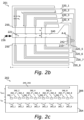
- Figure 2b describes in more detail a geometric layout of an example embodiment of a system 201 based on the system 200 described with reference to Figure 2a .
- the same principles discussed for the system 200 apply also to the system 200, and mostly particular details not already discussed for the system 200 will be described below.
- the system 201 includes a feedline having a one-port geometry, wherein RF signals 236 including both input and output signals (for both readout and control of the qubits) are provided at a single RF input/output port at an end of the feedline 240.
- the feedline 240 is also associated with a ground plane 250 which is provided in a same layer as the feedline 240.
- the ground plane 250 is structured such that it may be shared also with a plurality of resonators 220_1-N which are provided in a layer below that of the feedline 240 and the ground plane 250.
- the qubit arrangement 210 is arranged below a part 242 of the feedline, and each resonator 220_j is connected, in an end thereof not used for coupling to the feedline, to a respective qubit in the qubit arrangement 210.
- the feedline 240 and resonators 220_1-N are defined as having certain dimension.
- the feedline has a width w F .
- a separation distance between the ground plane 250 and the feedline 250 is s F .
- An overlap length between each resonator 220_1-N and the feedline 240 is l O .
- Each resonator 220_j (where j is an integer between 1 and N, and where N is the total number of resonators, and qubits) has a length l Rj along which the resonator in question runs along part of the ground plane.
- the remaining lengths of each resonator e.g.
- w Rj for resonator 220_j) of a resonator is much smaller than a separation s R (i.e. s Rj for resonator 220_j) between a resonator and the ground plane 250.
- s R separation i.e. s Rj for resonator 220_j
- the total lengths of resonators 220_j may thus be adapted such that enough discrimination between signals originating from different qubits is obtained. It is envisaged also that the cutouts in the ground plane 250 (wherein the corresponding feedline runs along the ground plane 250) may be tuned in order to achieve a desired resonant frequency.
- Figure 2c illustrates a cross section 202 of the system 201, including a cross-section of at least parts of the qubit arrangement 210, along the dashed line A-A in Figure 2b .
- the feedline 240 (or at least the part 242 thereof) is provided in a separate plane adjacent to that of the various resonators 220_1-N.
- the various resonators 220_1-N are used as (or at least connects to) gates 260_1-N arranged in another layer, separated from the layer of the feedline 240 by a dielectric 266 (of for example SiO 2 ).
- the qubit arrangement also includes various barrier gates 262_1-N, which together with the gates 260_1-N defined by (or at least connected to) the resonators 220_1-N define a plurality of quantum dots 263_1-N at the interface between the dielectric 266 and a (e.g. silicon) substrate 264. Additional gates and reservoirs (such as various confinement gates for confining electrons in dimensions extending perpendicular to the cross-section plane shown in Figure 2c to fully define the quantum dots, reservoir gates for controlled provision of electrons into/out of the various quantum dots, corresponding reservoirs, additional 2DEGs, etc.) and similar may also be included in the qubit arrangement, but are not shown in Figure 2c .
- the gates not formed by, or connected to, the resonators 220_1-N may be connected to various DC or low-frequency voltages, as provided e.g. by the DC and low-frequency signals 232 illustrated in Figure 2a .
- a separation distance between the layer of the feedline 250 and the layer of the resonators 220_1-N is t OX-R .
- a separation between the gates and the interface where the quantum dots 263_1-N are formed is tox.
- a width of a quantum dot 263_j is w D .
- a length of a quantum dot 263_j (e.g. in a cross-sectional plane perpendicular to that shown in Figure 2c ) is l D .
- a spacing between two nearby quantum dots 263_j is b D .
- Figure 2d schematically illustrates yet another example embodiment of a system 203 including six resonators 220_1-6 coupled to a qubit arrangement 210 which may for example also include six qubits. It is of course envisaged that also other number of resonators and/or qubits may be used, and the system 203 is only one possible envisaged example. This applies to any system disclosed herein, such as for example also the system 201 described with reference to Figure 2b , wherein the total number of qubits and/or resonators are not necessarily eight.
- the system 203 has a two-port geometry wherein an input port is arranged at one end of the feedline 240 (for receiving an RF input signal 237), and an output port is arranged at another end of the feedline 240 (for receiving an RF output signal 238).
- the qubit arrangement 210 is positioned at approximately the middle of (and below) the feedline 240.
- the full lengths l Rj of the various resonators are taken into account when determining the resonant frequency for each resonator.
- the width of the cutouts in the ground plane 250 for each resonator may be different, and/or that the lengths of the resonators outside of the ground plane 250 may be adapted accordingly, even though these lengths are envisaged as being small compared with the lengths l Rj of the sections of the resonators 220_j running along the ground plane 250 within their dedicated cutouts in the ground plane 250, as described earlier herein.
- a total length of e.g. resonator 220_1 does not need to exactly match that of the resonator 220_6; a total length of e.g. resonator 220_2 does not need to exactly match that of resonator 220_5, and similarly for resonators 220_3 and 220_4.
- the various dimensions given in e.g. Figures 2b, 2c and 2d may for example be the following: w F may be on the order of few micrometers (e.g. approximately 4.2 ⁇ m); s F may be on the order of few micrometers (e.g. approximately 3 ⁇ m) ; l F may be on the order of few millimeters (e.g. approximately 1 mm); l O may be on the order of few tens of micrometers (e.g. 40 ⁇ m) ; w Rj may be on the order of few tens of nanometers (e.g.
- s Rj may be on the order of a few micrometers (e.g. approximately 1 ⁇ m) ; l Rj may be on the order of fractions of millimeters to a few millimeters (e.g. approximately 0.5-1.1 mm); each l Rj may differ by e.g. approximately 10 %; t OX-R may be on the order of few tens of nanometers (e.g. approximately 20-40 nm, such as e.g. 30 nm); tox may be on the order of few nanometers (e.g. approximately 8 nm); w D may be on the order of few tens of nanometers (e.g.
- l D may be on the order of few tens of nanometers (e.g. approximately 50 nm), and bo may be on the order of few tens of nanometers (e.g. approximately 30 nm).
- the overlap distance l O between a resonator and the feedline is here on the order of few tens of micrometers
- a conventional system not according to the present disclosure requires overlap distances normally on the order of few hundreds of micrometers.
- the separation t OX-R between a resonator and a feedline is here on the order of few tens of nanometers
- the separation between a feedline and a resonator is at least some multiple of the separation distance between the feedline and its ground plane, i.e. at least few or even tens of micrometers.
- the dimensions of a system according to the present disclosure may thereby provide both an increased coupling strength and/or a reduced footprint of the system, as e.g. the overlap distances may be reduced while still obtaining a sufficient coupling strength, and vice versa.
- a same ground plane may be used for return current paths for both the feedline and resonator(s).
- the return current is an AC current
- capacitive coupling is envisaged as being distributed along e.g. the section of the resonator which runs along a cutout in the ground plane.
- a similar capacitive coupling also occurs between the feedline and the ground plane.
- Figures 2a to 2d illustrate various embodiments wherein the system includes multiple qubits
- the system may contain only a single qubit. Even with a single qubit, the benefit of the feedline and resonator in separate layers are present, as well as the benefit originating from having a reduced number of required input/output ports (as a result of using a same, single feedline for both readout and control of the qubit/qubits).
- the need for frequency multiplexing may of course be avoided at least in the sense of qubit readout. Pulses for readout and control may still have different frequencies.
- the present disclosure provides a system in which the use of a single, shared feedline is used for both readout and control of one or more qubits, where a ground plane is shared between the feedline and the one or more resonators, and where the feedline and resonator(s) are located in different planes separated by a dielectric.
- This allows to create a less complex structure, wherein the footprint may be reduced while still achieving sufficient capacitive coupling between e.g. the feedline and resonators in order to readout and control the qubit, and where the number of needed input/output ports may be reduced leading to even further reduction of complexity and footprint.
Landscapes
- Engineering & Computer Science (AREA)
- General Physics & Mathematics (AREA)
- Theoretical Computer Science (AREA)
- Physics & Mathematics (AREA)
- Mathematical Analysis (AREA)
- Computing Systems (AREA)
- Evolutionary Computation (AREA)
- Condensed Matter Physics & Semiconductors (AREA)
- Computational Mathematics (AREA)
- Mathematical Optimization (AREA)
- Pure & Applied Mathematics (AREA)
- Data Mining & Analysis (AREA)
- General Engineering & Computer Science (AREA)
- Mathematical Physics (AREA)
- Software Systems (AREA)
- Artificial Intelligence (AREA)
- Superconductor Devices And Manufacturing Methods Thereof (AREA)
- Control Of Motors That Do Not Use Commutators (AREA)
Claims (11)
- Integriertes System (201) für Quantenrechnung, umfassend:mindestens ein Halbleiter-Spin-Qubit (210);eine Zuleitung (240), die dazu konfiguriert ist, als Elektronen-Spin-Resonanz-, ESR, Antenne zur Steuerung des mindestens einen Halbleiter-Spin-Qubits zu dienen,mindestens einen Resonator (220_j), undeine Grundplatte (250), die sowohl der Zuleitung als auch dem mindestens einen Resonator gemeinsam ist,wobei der mindestens eine Resonator mit der Zuleitung kapazitiv gekoppelt ist, und zum Auslesen des mindestens einen Halbleiter-Spin-Qubits über die Zuleitung konfiguriert ist, undwobei die Zuleitung und der mindestens eine Resonator in angrenzenden Schichten angeordnet sind, die durch mindestens ein Dielektrikum getrennt sind.
- System nach Anspruch 1, wobei eine Dicke des Dielektrikums zwischen 20 nm und 40 nm liegt.
- System nach Anspruch 1 oder 2, ferner umfassend Funkfrequenz-, RF, Ein-/Ausgangsmittel, die an die Zuleitung angeschlossen sind.
- System nach Anspruch 3, wobei die RF-Ein-/Ausgangsmittel einen kombinierten RF-Ein-/Ausgangs-Port umfassen, der an das gleiche Ende der Zuleitung angeschlossen ist.
- System nach Anspruch 3, wobei die RF-Ein-/Ausgangsmittel einen RF-Eingangs-Port, der an ein Ende der Zuleitung angeschlossen ist, und einen RF-Ausgangs-Port, der an ein anderes Ende der Zuleitung angeschlossen ist, umfassen.
- System nach einem der vorhergehenden Ansprüche, wobei eine Impedanz des mindestens einen Resonators mindestens 1 kOhm beträgt.
- System nach einem der vorhergehenden Ansprüche, wobei ein Q-Faktor des mindestens einen Resonators in einem Bereich von 1000 bis 10000 liegt.
- System nach einem der vorhergehenden Ansprüche, wobei das System eine Vielzahl von Halbleiter-Spin-Qubits und eine Vielzahl von Resonatoren umfasst, und wobei jeder Resonator eine andere Resonanzfrequenz zum Auslesen der Vielzahl von Halbleiter-Spin-Qubits unter Verwendung von Frequenzmultiplex aufweist.
- System nach einem der vorhergehenden Ansprüche, wobei das mindestens eine Halbleiter-Spin-Qubit unter Verwendung mindestens eines Quantenpunktes umgesetzt ist.
- Verfahren zum Ausführen von Quantenrechnung unter Verwendung eines integrierten Systems nach einem der vorhergehenden Ansprüche, umfassend sowohl das Steuern als auch das Auslesen des Zustands des mindestens einen Halbleiter-Spin-Qubits unter Verwendung der Zuleitung.
- Verfahren nach Anspruch 10, umfassend sowohl das Steuern als auch das Auslesen der Zustände der Vielzahl von Halbleiter-Spin-Qubits unter Verwendung der Zuleitung und von Frequenzmultiplex.
Priority Applications (3)
| Application Number | Priority Date | Filing Date | Title |
|---|---|---|---|
| EP20216162.6A EP4016401B1 (de) | 2020-12-21 | 2020-12-21 | Steuerungs- und auslesetopologie für spin-qubits |
| US17/645,209 US12204996B2 (en) | 2020-12-21 | 2021-12-20 | Control and readout topology for spin qubits |
| CN202111564405.4A CN114648126B (zh) | 2020-12-21 | 2021-12-20 | 用于自旋量子比特的控制和读出拓扑结构 |
Applications Claiming Priority (1)
| Application Number | Priority Date | Filing Date | Title |
|---|---|---|---|
| EP20216162.6A EP4016401B1 (de) | 2020-12-21 | 2020-12-21 | Steuerungs- und auslesetopologie für spin-qubits |
Publications (2)
| Publication Number | Publication Date |
|---|---|
| EP4016401A1 EP4016401A1 (de) | 2022-06-22 |
| EP4016401B1 true EP4016401B1 (de) | 2023-07-05 |
Family
ID=73856457
Family Applications (1)
| Application Number | Title | Priority Date | Filing Date |
|---|---|---|---|
| EP20216162.6A Active EP4016401B1 (de) | 2020-12-21 | 2020-12-21 | Steuerungs- und auslesetopologie für spin-qubits |
Country Status (3)
| Country | Link |
|---|---|
| US (1) | US12204996B2 (de) |
| EP (1) | EP4016401B1 (de) |
| CN (1) | CN114648126B (de) |
Families Citing this family (3)
| Publication number | Priority date | Publication date | Assignee | Title |
|---|---|---|---|---|
| KR20230006328A (ko) * | 2021-07-02 | 2023-01-10 | 삼성전자주식회사 | 능동 서큘레이터 및 능동 서큘레이터를 포함하는 양자컴퓨터시스템 |
| CN117094403A (zh) * | 2023-06-25 | 2023-11-21 | 合肥国家实验室 | 用于量子计算的集成型调控设备 |
| WO2025231531A1 (en) * | 2024-05-10 | 2025-11-13 | Silicon Quantum Computing Pty Limited | Control systems for quantum processing devices |
Family Cites Families (8)
| Publication number | Priority date | Publication date | Assignee | Title |
|---|---|---|---|---|
| JP5679046B2 (ja) * | 2011-03-29 | 2015-03-04 | 日本電気株式会社 | デカップリング方法と給電線路設計装置並びに回路基板 |
| WO2015144388A1 (en) * | 2014-03-24 | 2015-10-01 | Koninklijke Philips N.V. | Magnetic resonance imaging rf antenna |
| EP3082073B1 (de) * | 2015-04-12 | 2019-01-16 | Hitachi Ltd. | Quanteninformationsverarbeitung |
| US11341426B2 (en) * | 2015-11-27 | 2022-05-24 | Photonic Inc. | Systems, devices, and methods to interact with quantum information stored in spins |
| US9680452B1 (en) * | 2016-10-17 | 2017-06-13 | International Business Machines Corporation | Sum frequency generator in the microwave domain for quantum communication and computation applications |
| US11171400B2 (en) * | 2017-09-07 | 2021-11-09 | Amherst College | Loop gap resonators for spin resonance spectroscopy |
| CN111465948B (zh) * | 2017-12-15 | 2024-04-02 | 谷歌有限责任公司 | 紧凑型多极量子比特测量滤波器 |
| US20230229952A1 (en) * | 2020-06-04 | 2023-07-20 | Silicon Quantum Computing Pty Limited | An advanced quantum processor architecture |
-
2020
- 2020-12-21 EP EP20216162.6A patent/EP4016401B1/de active Active
-
2021
- 2021-12-20 CN CN202111564405.4A patent/CN114648126B/zh active Active
- 2021-12-20 US US17/645,209 patent/US12204996B2/en active Active
Also Published As
| Publication number | Publication date |
|---|---|
| US20220198313A1 (en) | 2022-06-23 |
| US12204996B2 (en) | 2025-01-21 |
| CN114648126A (zh) | 2022-06-21 |
| CN114648126B (zh) | 2025-10-28 |
| EP4016401A1 (de) | 2022-06-22 |
Similar Documents
| Publication | Publication Date | Title |
|---|---|---|
| US12204996B2 (en) | Control and readout topology for spin qubits | |
| US11824248B2 (en) | Shielded bridges for quantum circuits | |
| US7932514B2 (en) | Microwave readout for flux-biased qubits | |
| US11537929B2 (en) | Superconducting interposer for the transmission of quantum information for quantum error correction | |
| JP6802266B2 (ja) | 超電導回路に埋め込まれたジョセフソン接合部の交差カー非線形性に基づく量子非破壊マイクロ波光子計数器、計数方法、および動作方法 | |
| US10546994B1 (en) | Architecture for coupling quantum bits using localized resonators | |
| CN107924490B (zh) | 量子信息处理系统 | |
| EP3516596B1 (de) | Hybride kinetische induktionsgeräte zum supraleitenden quantenrechnen | |
| US9985193B2 (en) | Architecture for coupling quantum bits using localized resonators | |
| CN114200282B (zh) | 测试器件以及采用测试器件进行测试的测试方法 | |
| US20200127187A1 (en) | Reducing surface loss and stray coupling in quantum devices using dielectric thinning | |
| KR20230005354A (ko) | 양자 컴퓨팅 애플리케이션을 위한 계층화된 하이브리드 양자 아키텍처 | |
| US20200403289A1 (en) | Transmission line resonator coupling | |
| US11777478B2 (en) | DC conversion of half- to quarter-wave resonators for crosstalk suppression in superconducting qubits | |
| Fallik et al. | CryoCMOS RF multiplexer for superconducting qubit control, readout and flux biasing at millikelvin temperatures with picowatt power consumption | |
| US20230153666A1 (en) | Semi-lossy purcell filter | |
| TW202534580A (zh) | 高頻串級讀出 |
Legal Events
| Date | Code | Title | Description |
|---|---|---|---|
| PUAI | Public reference made under article 153(3) epc to a published international application that has entered the european phase |
Free format text: ORIGINAL CODE: 0009012 |
|
| STAA | Information on the status of an ep patent application or granted ep patent |
Free format text: STATUS: THE APPLICATION HAS BEEN PUBLISHED |
|
| AK | Designated contracting states |
Kind code of ref document: A1 Designated state(s): AL AT BE BG CH CY CZ DE DK EE ES FI FR GB GR HR HU IE IS IT LI LT LU LV MC MK MT NL NO PL PT RO RS SE SI SK SM TR |
|
| STAA | Information on the status of an ep patent application or granted ep patent |
Free format text: STATUS: REQUEST FOR EXAMINATION WAS MADE |
|
| RBV | Designated contracting states (corrected) |
Designated state(s): AL AT BE BG CH CY CZ DE DK EE ES FI FR GB GR HR HU IE IS IT LI LT LU LV MC MK MT NL NO PL PT RO RS SE SI SK SM TR |
|
| REG | Reference to a national code |
Ref legal event code: R079 Ipc: G06N0010400000 Ref country code: DE Ref document number: 602020013274 Country of ref document: DE Free format text: PREVIOUS MAIN CLASS: G06N0010000000 |
|
| 17P | Request for examination filed |
Effective date: 20221208 |
|
| GRAP | Despatch of communication of intention to grant a patent |
Free format text: ORIGINAL CODE: EPIDOSNIGR1 |
|
| STAA | Information on the status of an ep patent application or granted ep patent |
Free format text: STATUS: GRANT OF PATENT IS INTENDED |
|
| RIC1 | Information provided on ipc code assigned before grant |
Ipc: H01L 29/423 20060101ALN20230113BHEP Ipc: H01L 29/66 20060101ALN20230113BHEP Ipc: B82Y 10/00 20110101ALN20230113BHEP Ipc: G06N 10/40 20220101AFI20230113BHEP |
|
| INTG | Intention to grant announced |
Effective date: 20230203 |
|
| GRAS | Grant fee paid |
Free format text: ORIGINAL CODE: EPIDOSNIGR3 |
|
| GRAA | (expected) grant |
Free format text: ORIGINAL CODE: 0009210 |
|
| STAA | Information on the status of an ep patent application or granted ep patent |
Free format text: STATUS: THE PATENT HAS BEEN GRANTED |
|
| P01 | Opt-out of the competence of the unified patent court (upc) registered |
Effective date: 20230513 |
|
| AK | Designated contracting states |
Kind code of ref document: B1 Designated state(s): AL AT BE BG CH CY CZ DE DK EE ES FI FR GB GR HR HU IE IS IT LI LT LU LV MC MK MT NL NO PL PT RO RS SE SI SK SM TR |
|
| REG | Reference to a national code |
Ref country code: CH Ref legal event code: EP |
|
| REG | Reference to a national code |
Ref country code: AT Ref legal event code: REF Ref document number: 1585522 Country of ref document: AT Kind code of ref document: T Effective date: 20230715 |
|
| REG | Reference to a national code |
Ref country code: DE Ref legal event code: R096 Ref document number: 602020013274 Country of ref document: DE |
|
| REG | Reference to a national code |
Ref country code: IE Ref legal event code: FG4D |
|
| REG | Reference to a national code |
Ref country code: LT Ref legal event code: MG9D |
|
| REG | Reference to a national code |
Ref country code: NL Ref legal event code: MP Effective date: 20230705 |
|
| REG | Reference to a national code |
Ref country code: AT Ref legal event code: MK05 Ref document number: 1585522 Country of ref document: AT Kind code of ref document: T Effective date: 20230705 |
|
| PG25 | Lapsed in a contracting state [announced via postgrant information from national office to epo] |
Ref country code: NL Free format text: LAPSE BECAUSE OF FAILURE TO SUBMIT A TRANSLATION OF THE DESCRIPTION OR TO PAY THE FEE WITHIN THE PRESCRIBED TIME-LIMIT Effective date: 20230705 |
|
| PG25 | Lapsed in a contracting state [announced via postgrant information from national office to epo] |
Ref country code: GR Free format text: LAPSE BECAUSE OF FAILURE TO SUBMIT A TRANSLATION OF THE DESCRIPTION OR TO PAY THE FEE WITHIN THE PRESCRIBED TIME-LIMIT Effective date: 20231006 |
|
| PG25 | Lapsed in a contracting state [announced via postgrant information from national office to epo] |
Ref country code: ES Free format text: LAPSE BECAUSE OF FAILURE TO SUBMIT A TRANSLATION OF THE DESCRIPTION OR TO PAY THE FEE WITHIN THE PRESCRIBED TIME-LIMIT Effective date: 20230705 |
|
| PG25 | Lapsed in a contracting state [announced via postgrant information from national office to epo] |
Ref country code: IS Free format text: LAPSE BECAUSE OF FAILURE TO SUBMIT A TRANSLATION OF THE DESCRIPTION OR TO PAY THE FEE WITHIN THE PRESCRIBED TIME-LIMIT Effective date: 20231105 |
|
| PG25 | Lapsed in a contracting state [announced via postgrant information from national office to epo] |
Ref country code: SE Free format text: LAPSE BECAUSE OF FAILURE TO SUBMIT A TRANSLATION OF THE DESCRIPTION OR TO PAY THE FEE WITHIN THE PRESCRIBED TIME-LIMIT Effective date: 20230705 Ref country code: RS Free format text: LAPSE BECAUSE OF FAILURE TO SUBMIT A TRANSLATION OF THE DESCRIPTION OR TO PAY THE FEE WITHIN THE PRESCRIBED TIME-LIMIT Effective date: 20230705 Ref country code: PT Free format text: LAPSE BECAUSE OF FAILURE TO SUBMIT A TRANSLATION OF THE DESCRIPTION OR TO PAY THE FEE WITHIN THE PRESCRIBED TIME-LIMIT Effective date: 20231106 Ref country code: NO Free format text: LAPSE BECAUSE OF FAILURE TO SUBMIT A TRANSLATION OF THE DESCRIPTION OR TO PAY THE FEE WITHIN THE PRESCRIBED TIME-LIMIT Effective date: 20231005 Ref country code: LV Free format text: LAPSE BECAUSE OF FAILURE TO SUBMIT A TRANSLATION OF THE DESCRIPTION OR TO PAY THE FEE WITHIN THE PRESCRIBED TIME-LIMIT Effective date: 20230705 Ref country code: LT Free format text: LAPSE BECAUSE OF FAILURE TO SUBMIT A TRANSLATION OF THE DESCRIPTION OR TO PAY THE FEE WITHIN THE PRESCRIBED TIME-LIMIT Effective date: 20230705 Ref country code: IS Free format text: LAPSE BECAUSE OF FAILURE TO SUBMIT A TRANSLATION OF THE DESCRIPTION OR TO PAY THE FEE WITHIN THE PRESCRIBED TIME-LIMIT Effective date: 20231105 Ref country code: HR Free format text: LAPSE BECAUSE OF FAILURE TO SUBMIT A TRANSLATION OF THE DESCRIPTION OR TO PAY THE FEE WITHIN THE PRESCRIBED TIME-LIMIT Effective date: 20230705 Ref country code: GR Free format text: LAPSE BECAUSE OF FAILURE TO SUBMIT A TRANSLATION OF THE DESCRIPTION OR TO PAY THE FEE WITHIN THE PRESCRIBED TIME-LIMIT Effective date: 20231006 Ref country code: FI Free format text: LAPSE BECAUSE OF FAILURE TO SUBMIT A TRANSLATION OF THE DESCRIPTION OR TO PAY THE FEE WITHIN THE PRESCRIBED TIME-LIMIT Effective date: 20230705 Ref country code: ES Free format text: LAPSE BECAUSE OF FAILURE TO SUBMIT A TRANSLATION OF THE DESCRIPTION OR TO PAY THE FEE WITHIN THE PRESCRIBED TIME-LIMIT Effective date: 20230705 Ref country code: AT Free format text: LAPSE BECAUSE OF FAILURE TO SUBMIT A TRANSLATION OF THE DESCRIPTION OR TO PAY THE FEE WITHIN THE PRESCRIBED TIME-LIMIT Effective date: 20230705 |
|
| PG25 | Lapsed in a contracting state [announced via postgrant information from national office to epo] |
Ref country code: PL Free format text: LAPSE BECAUSE OF FAILURE TO SUBMIT A TRANSLATION OF THE DESCRIPTION OR TO PAY THE FEE WITHIN THE PRESCRIBED TIME-LIMIT Effective date: 20230705 |
|
| REG | Reference to a national code |
Ref country code: DE Ref legal event code: R097 Ref document number: 602020013274 Country of ref document: DE |
|
| PG25 | Lapsed in a contracting state [announced via postgrant information from national office to epo] |
Ref country code: SM Free format text: LAPSE BECAUSE OF FAILURE TO SUBMIT A TRANSLATION OF THE DESCRIPTION OR TO PAY THE FEE WITHIN THE PRESCRIBED TIME-LIMIT Effective date: 20230705 Ref country code: RO Free format text: LAPSE BECAUSE OF FAILURE TO SUBMIT A TRANSLATION OF THE DESCRIPTION OR TO PAY THE FEE WITHIN THE PRESCRIBED TIME-LIMIT Effective date: 20230705 Ref country code: EE Free format text: LAPSE BECAUSE OF FAILURE TO SUBMIT A TRANSLATION OF THE DESCRIPTION OR TO PAY THE FEE WITHIN THE PRESCRIBED TIME-LIMIT Effective date: 20230705 Ref country code: DK Free format text: LAPSE BECAUSE OF FAILURE TO SUBMIT A TRANSLATION OF THE DESCRIPTION OR TO PAY THE FEE WITHIN THE PRESCRIBED TIME-LIMIT Effective date: 20230705 Ref country code: CZ Free format text: LAPSE BECAUSE OF FAILURE TO SUBMIT A TRANSLATION OF THE DESCRIPTION OR TO PAY THE FEE WITHIN THE PRESCRIBED TIME-LIMIT Effective date: 20230705 Ref country code: SK Free format text: LAPSE BECAUSE OF FAILURE TO SUBMIT A TRANSLATION OF THE DESCRIPTION OR TO PAY THE FEE WITHIN THE PRESCRIBED TIME-LIMIT Effective date: 20230705 |
|
| PLBE | No opposition filed within time limit |
Free format text: ORIGINAL CODE: 0009261 |
|
| STAA | Information on the status of an ep patent application or granted ep patent |
Free format text: STATUS: NO OPPOSITION FILED WITHIN TIME LIMIT |
|
| PG25 | Lapsed in a contracting state [announced via postgrant information from national office to epo] |
Ref country code: IT Free format text: LAPSE BECAUSE OF FAILURE TO SUBMIT A TRANSLATION OF THE DESCRIPTION OR TO PAY THE FEE WITHIN THE PRESCRIBED TIME-LIMIT Effective date: 20230705 |
|
| 26N | No opposition filed |
Effective date: 20240408 |
|
| PG25 | Lapsed in a contracting state [announced via postgrant information from national office to epo] |
Ref country code: SI Free format text: LAPSE BECAUSE OF FAILURE TO SUBMIT A TRANSLATION OF THE DESCRIPTION OR TO PAY THE FEE WITHIN THE PRESCRIBED TIME-LIMIT Effective date: 20230705 |
|
| REG | Reference to a national code |
Ref country code: CH Ref legal event code: PL |
|
| PG25 | Lapsed in a contracting state [announced via postgrant information from national office to epo] |
Ref country code: LU Free format text: LAPSE BECAUSE OF NON-PAYMENT OF DUE FEES Effective date: 20231221 |
|
| PG25 | Lapsed in a contracting state [announced via postgrant information from national office to epo] |
Ref country code: MC Free format text: LAPSE BECAUSE OF FAILURE TO SUBMIT A TRANSLATION OF THE DESCRIPTION OR TO PAY THE FEE WITHIN THE PRESCRIBED TIME-LIMIT Effective date: 20230705 |
|
| REG | Reference to a national code |
Ref country code: BE Ref legal event code: MM Effective date: 20231231 |
|
| PG25 | Lapsed in a contracting state [announced via postgrant information from national office to epo] |
Ref country code: MC Free format text: LAPSE BECAUSE OF FAILURE TO SUBMIT A TRANSLATION OF THE DESCRIPTION OR TO PAY THE FEE WITHIN THE PRESCRIBED TIME-LIMIT Effective date: 20230705 Ref country code: LU Free format text: LAPSE BECAUSE OF NON-PAYMENT OF DUE FEES Effective date: 20231221 |
|
| REG | Reference to a national code |
Ref country code: IE Ref legal event code: MM4A |
|
| PG25 | Lapsed in a contracting state [announced via postgrant information from national office to epo] |
Ref country code: IE Free format text: LAPSE BECAUSE OF NON-PAYMENT OF DUE FEES Effective date: 20231221 |
|
| PG25 | Lapsed in a contracting state [announced via postgrant information from national office to epo] |
Ref country code: BE Free format text: LAPSE BECAUSE OF NON-PAYMENT OF DUE FEES Effective date: 20231231 |
|
| PG25 | Lapsed in a contracting state [announced via postgrant information from national office to epo] |
Ref country code: FR Free format text: LAPSE BECAUSE OF NON-PAYMENT OF DUE FEES Effective date: 20231231 |
|
| PG25 | Lapsed in a contracting state [announced via postgrant information from national office to epo] |
Ref country code: CH Free format text: LAPSE BECAUSE OF NON-PAYMENT OF DUE FEES Effective date: 20231231 |
|
| PG25 | Lapsed in a contracting state [announced via postgrant information from national office to epo] |
Ref country code: IE Free format text: LAPSE BECAUSE OF NON-PAYMENT OF DUE FEES Effective date: 20231221 Ref country code: FR Free format text: LAPSE BECAUSE OF NON-PAYMENT OF DUE FEES Effective date: 20231231 Ref country code: CH Free format text: LAPSE BECAUSE OF NON-PAYMENT OF DUE FEES Effective date: 20231231 Ref country code: BE Free format text: LAPSE BECAUSE OF NON-PAYMENT OF DUE FEES Effective date: 20231231 |
|
| PG25 | Lapsed in a contracting state [announced via postgrant information from national office to epo] |
Ref country code: BG Free format text: LAPSE BECAUSE OF FAILURE TO SUBMIT A TRANSLATION OF THE DESCRIPTION OR TO PAY THE FEE WITHIN THE PRESCRIBED TIME-LIMIT Effective date: 20230705 |
|
| PG25 | Lapsed in a contracting state [announced via postgrant information from national office to epo] |
Ref country code: BG Free format text: LAPSE BECAUSE OF FAILURE TO SUBMIT A TRANSLATION OF THE DESCRIPTION OR TO PAY THE FEE WITHIN THE PRESCRIBED TIME-LIMIT Effective date: 20230705 |
|
| PG25 | Lapsed in a contracting state [announced via postgrant information from national office to epo] |
Ref country code: CY Free format text: LAPSE BECAUSE OF FAILURE TO SUBMIT A TRANSLATION OF THE DESCRIPTION OR TO PAY THE FEE WITHIN THE PRESCRIBED TIME-LIMIT; INVALID AB INITIO Effective date: 20201221 |
|
| PG25 | Lapsed in a contracting state [announced via postgrant information from national office to epo] |
Ref country code: HU Free format text: LAPSE BECAUSE OF FAILURE TO SUBMIT A TRANSLATION OF THE DESCRIPTION OR TO PAY THE FEE WITHIN THE PRESCRIBED TIME-LIMIT; INVALID AB INITIO Effective date: 20201221 |
|
| GBPC | Gb: european patent ceased through non-payment of renewal fee |
Effective date: 20241221 |
|
| PG25 | Lapsed in a contracting state [announced via postgrant information from national office to epo] |
Ref country code: GB Free format text: LAPSE BECAUSE OF NON-PAYMENT OF DUE FEES Effective date: 20241221 |
|
| PG25 | Lapsed in a contracting state [announced via postgrant information from national office to epo] |
Ref country code: TR Free format text: LAPSE BECAUSE OF FAILURE TO SUBMIT A TRANSLATION OF THE DESCRIPTION OR TO PAY THE FEE WITHIN THE PRESCRIBED TIME-LIMIT Effective date: 20230705 |
|
| PGFP | Annual fee paid to national office [announced via postgrant information from national office to epo] |
Ref country code: DE Payment date: 20251126 Year of fee payment: 6 |