EP4016278A1 - Infinitely expandable display device - Google Patents
Infinitely expandable display device Download PDFInfo
- Publication number
- EP4016278A1 EP4016278A1 EP21207866.1A EP21207866A EP4016278A1 EP 4016278 A1 EP4016278 A1 EP 4016278A1 EP 21207866 A EP21207866 A EP 21207866A EP 4016278 A1 EP4016278 A1 EP 4016278A1
- Authority
- EP
- European Patent Office
- Prior art keywords
- switch
- signal
- circuit
- display device
- data
- Prior art date
- Legal status (The legal status is an assumption and is not a legal conclusion. Google has not performed a legal analysis and makes no representation as to the accuracy of the status listed.)
- Pending
Links
Images





Classifications
-
- G—PHYSICS
- G09—EDUCATION; CRYPTOGRAPHY; DISPLAY; ADVERTISING; SEALS
- G09G—ARRANGEMENTS OR CIRCUITS FOR CONTROL OF INDICATING DEVICES USING STATIC MEANS TO PRESENT VARIABLE INFORMATION
- G09G3/00—Control arrangements or circuits, of interest only in connection with visual indicators other than cathode-ray tubes
- G09G3/20—Control arrangements or circuits, of interest only in connection with visual indicators other than cathode-ray tubes for presentation of an assembly of a number of characters, e.g. a page, by composing the assembly by combination of individual elements arranged in a matrix no fixed position being assigned to or needed to be assigned to the individual characters or partial characters
- G09G3/22—Control arrangements or circuits, of interest only in connection with visual indicators other than cathode-ray tubes for presentation of an assembly of a number of characters, e.g. a page, by composing the assembly by combination of individual elements arranged in a matrix no fixed position being assigned to or needed to be assigned to the individual characters or partial characters using controlled light sources
- G09G3/30—Control arrangements or circuits, of interest only in connection with visual indicators other than cathode-ray tubes for presentation of an assembly of a number of characters, e.g. a page, by composing the assembly by combination of individual elements arranged in a matrix no fixed position being assigned to or needed to be assigned to the individual characters or partial characters using controlled light sources using electroluminescent panels
- G09G3/32—Control arrangements or circuits, of interest only in connection with visual indicators other than cathode-ray tubes for presentation of an assembly of a number of characters, e.g. a page, by composing the assembly by combination of individual elements arranged in a matrix no fixed position being assigned to or needed to be assigned to the individual characters or partial characters using controlled light sources using electroluminescent panels semiconductive, e.g. using light-emitting diodes [LED]
- G09G3/3208—Control arrangements or circuits, of interest only in connection with visual indicators other than cathode-ray tubes for presentation of an assembly of a number of characters, e.g. a page, by composing the assembly by combination of individual elements arranged in a matrix no fixed position being assigned to or needed to be assigned to the individual characters or partial characters using controlled light sources using electroluminescent panels semiconductive, e.g. using light-emitting diodes [LED] organic, e.g. using organic light-emitting diodes [OLED]
- G09G3/3275—Details of drivers for data electrodes
-
- G—PHYSICS
- G09—EDUCATION; CRYPTOGRAPHY; DISPLAY; ADVERTISING; SEALS
- G09G—ARRANGEMENTS OR CIRCUITS FOR CONTROL OF INDICATING DEVICES USING STATIC MEANS TO PRESENT VARIABLE INFORMATION
- G09G3/00—Control arrangements or circuits, of interest only in connection with visual indicators other than cathode-ray tubes
- G09G3/20—Control arrangements or circuits, of interest only in connection with visual indicators other than cathode-ray tubes for presentation of an assembly of a number of characters, e.g. a page, by composing the assembly by combination of individual elements arranged in a matrix no fixed position being assigned to or needed to be assigned to the individual characters or partial characters
- G09G3/2092—Details of a display terminals using a flat panel, the details relating to the control arrangement of the display terminal and to the interfaces thereto
- G09G3/2096—Details of the interface to the display terminal specific for a flat panel
-
- G—PHYSICS
- G09—EDUCATION; CRYPTOGRAPHY; DISPLAY; ADVERTISING; SEALS
- G09F—DISPLAYING; ADVERTISING; SIGNS; LABELS OR NAME-PLATES; SEALS
- G09F9/00—Indicating arrangements for variable information in which the information is built-up on a support by selection or combination of individual elements
- G09F9/30—Indicating arrangements for variable information in which the information is built-up on a support by selection or combination of individual elements in which the desired character or characters are formed by combining individual elements
- G09F9/302—Indicating arrangements for variable information in which the information is built-up on a support by selection or combination of individual elements in which the desired character or characters are formed by combining individual elements characterised by the form or geometrical disposition of the individual elements
- G09F9/3026—Video wall, i.e. stackable semiconductor matrix display modules
-
- G—PHYSICS
- G09—EDUCATION; CRYPTOGRAPHY; DISPLAY; ADVERTISING; SEALS
- G09G—ARRANGEMENTS OR CIRCUITS FOR CONTROL OF INDICATING DEVICES USING STATIC MEANS TO PRESENT VARIABLE INFORMATION
- G09G3/00—Control arrangements or circuits, of interest only in connection with visual indicators other than cathode-ray tubes
- G09G3/20—Control arrangements or circuits, of interest only in connection with visual indicators other than cathode-ray tubes for presentation of an assembly of a number of characters, e.g. a page, by composing the assembly by combination of individual elements arranged in a matrix no fixed position being assigned to or needed to be assigned to the individual characters or partial characters
- G09G3/22—Control arrangements or circuits, of interest only in connection with visual indicators other than cathode-ray tubes for presentation of an assembly of a number of characters, e.g. a page, by composing the assembly by combination of individual elements arranged in a matrix no fixed position being assigned to or needed to be assigned to the individual characters or partial characters using controlled light sources
- G09G3/30—Control arrangements or circuits, of interest only in connection with visual indicators other than cathode-ray tubes for presentation of an assembly of a number of characters, e.g. a page, by composing the assembly by combination of individual elements arranged in a matrix no fixed position being assigned to or needed to be assigned to the individual characters or partial characters using controlled light sources using electroluminescent panels
- G09G3/32—Control arrangements or circuits, of interest only in connection with visual indicators other than cathode-ray tubes for presentation of an assembly of a number of characters, e.g. a page, by composing the assembly by combination of individual elements arranged in a matrix no fixed position being assigned to or needed to be assigned to the individual characters or partial characters using controlled light sources using electroluminescent panels semiconductive, e.g. using light-emitting diodes [LED]
- G09G3/3208—Control arrangements or circuits, of interest only in connection with visual indicators other than cathode-ray tubes for presentation of an assembly of a number of characters, e.g. a page, by composing the assembly by combination of individual elements arranged in a matrix no fixed position being assigned to or needed to be assigned to the individual characters or partial characters using controlled light sources using electroluminescent panels semiconductive, e.g. using light-emitting diodes [LED] organic, e.g. using organic light-emitting diodes [OLED]
-
- G—PHYSICS
- G09—EDUCATION; CRYPTOGRAPHY; DISPLAY; ADVERTISING; SEALS
- G09G—ARRANGEMENTS OR CIRCUITS FOR CONTROL OF INDICATING DEVICES USING STATIC MEANS TO PRESENT VARIABLE INFORMATION
- G09G3/00—Control arrangements or circuits, of interest only in connection with visual indicators other than cathode-ray tubes
- G09G3/20—Control arrangements or circuits, of interest only in connection with visual indicators other than cathode-ray tubes for presentation of an assembly of a number of characters, e.g. a page, by composing the assembly by combination of individual elements arranged in a matrix no fixed position being assigned to or needed to be assigned to the individual characters or partial characters
- G09G3/22—Control arrangements or circuits, of interest only in connection with visual indicators other than cathode-ray tubes for presentation of an assembly of a number of characters, e.g. a page, by composing the assembly by combination of individual elements arranged in a matrix no fixed position being assigned to or needed to be assigned to the individual characters or partial characters using controlled light sources
- G09G3/30—Control arrangements or circuits, of interest only in connection with visual indicators other than cathode-ray tubes for presentation of an assembly of a number of characters, e.g. a page, by composing the assembly by combination of individual elements arranged in a matrix no fixed position being assigned to or needed to be assigned to the individual characters or partial characters using controlled light sources using electroluminescent panels
- G09G3/32—Control arrangements or circuits, of interest only in connection with visual indicators other than cathode-ray tubes for presentation of an assembly of a number of characters, e.g. a page, by composing the assembly by combination of individual elements arranged in a matrix no fixed position being assigned to or needed to be assigned to the individual characters or partial characters using controlled light sources using electroluminescent panels semiconductive, e.g. using light-emitting diodes [LED]
- G09G3/3208—Control arrangements or circuits, of interest only in connection with visual indicators other than cathode-ray tubes for presentation of an assembly of a number of characters, e.g. a page, by composing the assembly by combination of individual elements arranged in a matrix no fixed position being assigned to or needed to be assigned to the individual characters or partial characters using controlled light sources using electroluminescent panels semiconductive, e.g. using light-emitting diodes [LED] organic, e.g. using organic light-emitting diodes [OLED]
- G09G3/3225—Control arrangements or circuits, of interest only in connection with visual indicators other than cathode-ray tubes for presentation of an assembly of a number of characters, e.g. a page, by composing the assembly by combination of individual elements arranged in a matrix no fixed position being assigned to or needed to be assigned to the individual characters or partial characters using controlled light sources using electroluminescent panels semiconductive, e.g. using light-emitting diodes [LED] organic, e.g. using organic light-emitting diodes [OLED] using an active matrix
- G09G3/3233—Control arrangements or circuits, of interest only in connection with visual indicators other than cathode-ray tubes for presentation of an assembly of a number of characters, e.g. a page, by composing the assembly by combination of individual elements arranged in a matrix no fixed position being assigned to or needed to be assigned to the individual characters or partial characters using controlled light sources using electroluminescent panels semiconductive, e.g. using light-emitting diodes [LED] organic, e.g. using organic light-emitting diodes [OLED] using an active matrix with pixel circuitry controlling the current through the light-emitting element
-
- H—ELECTRICITY
- H10—SEMICONDUCTOR DEVICES; ELECTRIC SOLID-STATE DEVICES NOT OTHERWISE PROVIDED FOR
- H10K—ORGANIC ELECTRIC SOLID-STATE DEVICES
- H10K59/00—Integrated devices, or assemblies of multiple devices, comprising at least one organic light-emitting element covered by group H10K50/00
- H10K59/10—OLED displays
- H10K59/18—Tiled displays
-
- G—PHYSICS
- G06—COMPUTING OR CALCULATING; COUNTING
- G06F—ELECTRIC DIGITAL DATA PROCESSING
- G06F3/00—Input arrangements for transferring data to be processed into a form capable of being handled by the computer; Output arrangements for transferring data from processing unit to output unit, e.g. interface arrangements
- G06F3/14—Digital output to display device ; Cooperation and interconnection of the display device with other functional units
- G06F3/1423—Digital output to display device ; Cooperation and interconnection of the display device with other functional units controlling a plurality of local displays, e.g. CRT and flat panel display
- G06F3/1446—Digital output to display device ; Cooperation and interconnection of the display device with other functional units controlling a plurality of local displays, e.g. CRT and flat panel display display composed of modules, e.g. video walls
-
- G—PHYSICS
- G09—EDUCATION; CRYPTOGRAPHY; DISPLAY; ADVERTISING; SEALS
- G09G—ARRANGEMENTS OR CIRCUITS FOR CONTROL OF INDICATING DEVICES USING STATIC MEANS TO PRESENT VARIABLE INFORMATION
- G09G2300/00—Aspects of the constitution of display devices
- G09G2300/02—Composition of display devices
- G09G2300/026—Video wall, i.e. juxtaposition of a plurality of screens to create a display screen of bigger dimensions
-
- G—PHYSICS
- G09—EDUCATION; CRYPTOGRAPHY; DISPLAY; ADVERTISING; SEALS
- G09G—ARRANGEMENTS OR CIRCUITS FOR CONTROL OF INDICATING DEVICES USING STATIC MEANS TO PRESENT VARIABLE INFORMATION
- G09G2300/00—Aspects of the constitution of display devices
- G09G2300/04—Structural and physical details of display devices
- G09G2300/0421—Structural details of the set of electrodes
- G09G2300/0426—Layout of electrodes and connections
-
- G—PHYSICS
- G09—EDUCATION; CRYPTOGRAPHY; DISPLAY; ADVERTISING; SEALS
- G09G—ARRANGEMENTS OR CIRCUITS FOR CONTROL OF INDICATING DEVICES USING STATIC MEANS TO PRESENT VARIABLE INFORMATION
- G09G2300/00—Aspects of the constitution of display devices
- G09G2300/08—Active matrix structure, i.e. with use of active elements, inclusive of non-linear two terminal elements, in the pixels together with light emitting or modulating elements
- G09G2300/0809—Several active elements per pixel in active matrix panels
- G09G2300/0842—Several active elements per pixel in active matrix panels forming a memory circuit, e.g. a dynamic memory with one capacitor
-
- G—PHYSICS
- G09—EDUCATION; CRYPTOGRAPHY; DISPLAY; ADVERTISING; SEALS
- G09G—ARRANGEMENTS OR CIRCUITS FOR CONTROL OF INDICATING DEVICES USING STATIC MEANS TO PRESENT VARIABLE INFORMATION
- G09G2310/00—Command of the display device
- G09G2310/08—Details of timing specific for flat panels, other than clock recovery
-
- G—PHYSICS
- G09—EDUCATION; CRYPTOGRAPHY; DISPLAY; ADVERTISING; SEALS
- G09G—ARRANGEMENTS OR CIRCUITS FOR CONTROL OF INDICATING DEVICES USING STATIC MEANS TO PRESENT VARIABLE INFORMATION
- G09G2320/00—Control of display operating conditions
- G09G2320/02—Improving the quality of display appearance
- G09G2320/029—Improving the quality of display appearance by monitoring one or more pixels in the display panel, e.g. by monitoring a fixed reference pixel
- G09G2320/0295—Improving the quality of display appearance by monitoring one or more pixels in the display panel, e.g. by monitoring a fixed reference pixel by monitoring each display pixel
-
- G—PHYSICS
- G09—EDUCATION; CRYPTOGRAPHY; DISPLAY; ADVERTISING; SEALS
- G09G—ARRANGEMENTS OR CIRCUITS FOR CONTROL OF INDICATING DEVICES USING STATIC MEANS TO PRESENT VARIABLE INFORMATION
- G09G2360/00—Aspects of the architecture of display systems
- G09G2360/04—Display device controller operating with a plurality of display units
-
- G—PHYSICS
- G09—EDUCATION; CRYPTOGRAPHY; DISPLAY; ADVERTISING; SEALS
- G09G—ARRANGEMENTS OR CIRCUITS FOR CONTROL OF INDICATING DEVICES USING STATIC MEANS TO PRESENT VARIABLE INFORMATION
- G09G2370/00—Aspects of data communication
- G09G2370/08—Details of image data interface between the display device controller and the data line driver circuit
-
- G—PHYSICS
- G09—EDUCATION; CRYPTOGRAPHY; DISPLAY; ADVERTISING; SEALS
- G09G—ARRANGEMENTS OR CIRCUITS FOR CONTROL OF INDICATING DEVICES USING STATIC MEANS TO PRESENT VARIABLE INFORMATION
- G09G2370/00—Aspects of data communication
- G09G2370/10—Use of a protocol of communication by packets in interfaces along the display data pipeline
Definitions
- the present disclosure relates to an infinitely expandable display device having expandability.
- An infinitely expandable display device forms a screen by connecting a plurality of display units and has the advantage that the screen size can be increased as necessary.
- each display unit of an infinitely expandable display device includes a control printed circuit board and an application-specific integrated circuit mounted thereon, and thus a connection structure of display units is complicated and an additional data processing operation for image synchronization is required.
- the present disclosure provides an infinitely expandable display device capable of simplifying a connection structure of display units and a data processing operation.
- An invention is set out in the independent claims.
- An infinitely expandable display device includes a plurality of display units including a plurality of data drivers connected through a bidirectional interface circuit, and a timing controller commonly connected to the display units through the bidirectional interface circuit.
- Each of the data drivers includes a first reception circuit EPI RX configured to receive a first interface signal in a first direction, a first transmission circuit EPI TX configured to transmit the first interface signal in the first direction, a second reception circuit RBUF configured to receive a second interface signal in a second direction opposite the first direction, a second transmission circuit TBUF configured to transmit the second interface signal in the second direction, and a switch circuit SWP connected to the first transmission circuit EPI TX, the second transmission circuit TBUF, and the second reception circuit RBUF.
- constituent elements included in the various embodiments of the present disclosure, the constituent elements are interpreted as including an error range even if there is no explicit description thereof.
- FIG. 1 is a diagram schematically showing an infinitely expandable display device according to an embodiment of the present disclosure.
- FIG. 2 is a diagram showing an exemplary resolution according to a driving unit of the infinitely expandable display device shown in FIG. 1 .
- FIG. 3 is a diagram showing a configuration of a display unit in the infinitely expandable display device.
- FIG. 4 is a diagram showing that data drivers of display units are commonly connected to a single control printed circuit board.
- FIG. 5 is a diagram showing a configuration of connection between a data driver and peripheral circuits in a display unit.
- FIG. 6 is a diagram showing a configuration of connection between a timing controller and display units through connection cables.
- references to an infinitely expandable display device may be used to indicate that it is possible to connect further display units to an existing plurality of display units of the display device, for example in a modular manner, in order to expand the display area of the display device.
- references to a timing controller being commonly connected to the display units through a bidirectional interface circuit may refer to the timing controller being connected to all of, or at least to a plurality of, the display units, or to the data drivers thereof, through the bidirectional interface circuit.
- the infinitely expandable display device includes a set board and a cabinet.
- the cabinet includes a plurality of display units connected through a bidirectional interface circuit to construct a screen.
- the full resolution of the large screen is determined by the sum of unit resolutions of the display units. For example, if the cabinet is composed of 16 display units having a unit resolution of 480*270, as shown in FIG. 2 , the full resolution of the cabinet is 1920*1080.
- the display units may be implemented as an electroluminescent display type capable of sensing driving characteristics of pixels.
- the technical spirit of the present disclosure is not limited to the method of implementing the display units.
- a gap (i.e., seam size) between the display units is designed to be less than a gap between pixels (i.e., pixel pitch) in order to achieve zero bezel.
- the zero bezel improves visibility and readability of the screen.
- the display units are connected through a cascading internal interface circuit to sequentially transfer image data generated in the set board.
- Each display unit corresponds to an electroluminescent display device including a display panel in which pixels are formed and a panel driving circuit for driving the display panel.
- the panel driving circuit includes a data driver and a gate driver.
- a pixel array as shown in FIG. 3 is formed on the front side of the display panel.
- the pixel array may include a plurality of sub-pixels and signal lines for supplying a driving voltage to the plurality of sub-pixels.
- These signal lines may include data lines DL for transmitting data voltages Vdata, gate lines GL1 and GL2 for transmitting gate signals SCAN and SEN, and readout lines RL for supplying a reference voltage VREF and sensing pixel driving characteristics Vsen.
- the signal lines disposed in the pixel array may further include a driving voltage line for transmitting a high-level pixel voltage EVDD.
- the data lines DL and the readout lines RL may extend in a first direction on the pixel array and the gate lines GL1 and GL2 may extend in a second direction perpendicular to the first direction. These signal lines may be connected to a pixel circuit of each sub-pixel and connected to the panel driving circuit.
- a low-level pixel voltage EVSS may be supplied to the pixel array.
- the low-level pixel voltage EVSS may be a common voltage applied to all sub-pixels.
- the low-level pixel voltage EVSS may be applied as a higher voltage in a sensing mode for driving characteristic detection than in a display mode for image writing, but the present disclosure is not limited thereto.
- a plurality of sub-pixels may constitute a single pixel.
- R (red), W (white), G (green), and B (blue) sub-pixels neighboring in the first direction may constitute a single pixel.
- R, G, and B sub-pixels may constitute a single pixel.
- W sub-pixels may be omitted from the pixel array.
- R, W, G, and B sub-pixels have the same pixel circuit configuration although they have different luminescent materials forming light-emitting elements.
- a sub-pixel may include a light-emitting element OLED, a driving TFT DT, switching TFTs ST1 and ST2, and a storage capacitor Cst, as shown in FIG. 3 .
- the driving TFT DT and the switching TFTs ST1 and ST2 may be implemented as NMOSs, but the present disclosure is not limited thereto.
- the light-emitting element OLED emits light with intensity corresponding to pixel current input from the driving TFT DT.
- the light-emitting element OLED may be implemented as an organic light-emitting diode including an organic emission layer or an inorganic light-emitting diode including an inorganic emission layer.
- An anode of the light-emitting element OLED is connected to a second node N2 and a cathode thereof is connected to an input terminal to which the low-level pixel voltage EVSS is applied.
- the driving TFT DT is a driving element that generates pixel current corresponding to a gate-source voltage.
- a gate electrode of the driving TFT DT is connected to a first node N1, a first electrode (drain electrode) thereof is connected to an input terminal to which the high-level pixel voltage EVDD is applied, and a second electrode (source electrode) thereof is connected to the second node N2.
- the switching TFTs ST1 and ST2 are switching elements that set the gate-source voltage of the driving TFT DT and connect the second electrode of the driving TFT DT to the readout lines RL.
- the first switching TFT ST1 is connected between a data line DL and the first node N1 and is turned on according to the first gate signal SCAN from the first gate line GL1.
- the first switching TFT ST1 is turned on during programming in the display mode and the sensing mode.
- a data voltage Vdata for display or sensing is applied to the first node N1.
- the gate electrode of the first switching TFT ST1 is connected to the first gate line GL1, the first electrode thereof is connected to the data line DL, and the second electrode thereof is connected to the first node N1.
- the second switching TFT ST2 is connected between a readout line RL and the second node N2 and is turned on according to the second gate signal SEN from the second gate line GL2.
- the second switching TFT ST2 is turned on during programming in the display mode and the sensing mode to apply the reference voltage VREF to the second node N2.
- the second switching TFT ST2 is also turned on during a sensing operation after set-up in the sensing mode to transfer a source node voltage (or a source voltage) of the driving TFT DT to the readout line RL. Then, a sensing voltage Vsen corresponding to the source voltage is stored in a parasitic capacitor Cp of the readout line RL.
- the gate electrode of the second switching TFT ST2 is connected to the second gate line GL2, the first electrode thereof is connected to the readout line RL, and the second electrode thereof is connected to the second node N2.
- the storage capacitor Cst is connected between the first node N1 and the second node N2 and maintains the gate-source voltage of the driving TFT DT for a predetermined time.
- the gate-source voltage of the driving TFT DT is programmed to a difference voltage between the data voltage Vdata for display and the reference voltage VREF in the display mode and is programmed to a difference voltage between the data voltage Vdata for sensing and the reference voltage VREF in the sensing mode.
- pixel current corresponding to the gate-source voltage of the driving TFT DT flows through the driving TFT DT and thus the light-emitting element OLED emits light according to the pixel current.
- pixel current corresponding to the gate-source voltage of the driving TFT DT flows through the driving TFT DT and thus a source node voltage of the driving TFT DT changes according to the pixel current. Since the source node voltage changes according to driving characteristics of the driving TFT DT, change in the driving characteristics of the driving TFT DT may be detected through a sensing voltage Vsen corresponding to the source node voltage.
- the low-level pixel voltage EVSS is applied as a voltage higher than the operating point voltage of the light-emitting element OLED in the sensing mode, and thus the pixel current of the driving TFT DT does not flow to the light-emitting element OLED and flows only through the readout line RL. Accordingly, sensing reliability can be improved because the source node voltage is reflected in the sensing voltage Vsen within a short time.
- first and second gate signals SCAN and SEN may be unified and the first and second gate lines GL1 and GL2 may be unified.
- the sub-pixel configuration may be modified to be suitable for double rate driving.
- each display unit does not individually include an application specific integrated circuit (ASIC).
- ASIC application specific integrated circuit
- operations of the display units are controlled by a single timing controller TCON through bidirectional communication. Accordingly, a connection structure of the display units is simplified and an additional data processing operation for image synchronization is not required.
- the display units include a plurality of data drivers DIC connected through a bidirectional interface circuit.
- the timing controller TCON is mounted on a control printed circuit board C-PCB and is connected to the data drivers DIC through a bidirectional interface circuit.
- the bidirectional interface circuits may be connected through a bidirectional communication cable.
- the bidirectional interface circuits may be implemented as an embedded panel interface (EPI).
- the data drivers DIC may be positioned on the backside of a display panel, as shown in FIG. 5 .
- a source printed circuit board S-PCB is additionally positioned on the backside of the display unit.
- a conductive film COF in which the data driver DIC is mounted is bonded to the source printed circuit board S-PCB.
- the source printed circuit board S-PCB includes a first connection terminal CTX and a second connection terminal CRX to be connected to a bidirectional communication cable CBL, as shown in FIG. 6 .
- the control printed circuit board C-PCB also includes the first connection terminal CTX and the second connection terminal CRX to be connected to the bidirectional communication cable CBL.
- the timing controller TCON is electrically connected to the data drivers DIC, and a first interface signal (hereinafter, an EPI signal) in a first direction and a second interface signal (hereinafter, an EPI feedback signal) in a second direction that is the opposite direction to the first direction are transmitted and received between the data drivers DIC and the timing controller TCON electrically connected to it.
- a first interface signal hereinafter, an EPI signal
- a second interface signal hereinafter, an EPI feedback signal
- the first/second directions may point along a column of the display units (e.g. in the 'up-down' direction as shown in FIG. 1 ).
- the first direction may point upwards towards the top of the display and the second direction may point downwards towards the bottom of the display.
- the first direction may point downwards towards the bottom of the display and the second direction may point upwards towards the top of the display.
- the first/second directions may point along a row of the display units (e.g. in the left-right' direction as shown in FIG. 1 ).
- the first direction may point rightwards towards the right edge of the display and the second direction may point leftwards towards the left edge of the display.
- first direction may point leftwards towards the left of the display and the second direction may point rightwards towards the right of the display.
- Other orientations, directions, and arrangements of display units are possible and considered within the present disclosure.
- references to a second direction being opposite a first direction may be used to indicate that, whereas transmitting a signal in a first direction may comprise transmitting a signal from a first display unit to a second display unit, receiving a signal in the second direction may comprise receiving a signal from the second display unit at the first display unit.
- the data driver DIC includes a digital-to-analog converter DAC that generates a data voltage Vdata, a sensing circuit SENU, and an analog-to-digital converter ADC.
- the digital-to-analog converter DAC converts image data supplied from the timing controller TCON into the data voltage Vdata for display according to a timing control signal and then provides the data voltage Vdata to the data lines DL in the display mode.
- the digital-to-analog converter DAC generates the data voltage Vdata for sensing and then provides the data voltage Vdata for sensing to the data lines DL in the sensing mode.
- the sensing circuit SENU provides the reference voltage VREF to the readout lines RL in the display mode.
- the sensing circuit SENU provides the reference voltage VREF to the readout lines RL and then samples a sensing voltage Vsen charged in the readout lines RL in the sensing mode.
- the sensing circuit SENU includes a reference voltage switch SPRE connected between the readout line RL and a reference voltage VREF input terminal, and a sampling switch SAM connected between the readout line RL and the analog-to-digital converter ADC.
- the reference voltage switch SPRE is turned on only in a programming period of the display mode and the sensing mode and the sampling switch SAM is turned on only in a sampling period of the sensing mode.
- the analog-to-digital converter ADC performs digital processing on a sampling voltage generated when the sampling switch SAM is turned on to output sensing result data SDATA in the sensing mode.
- the sensing result data SDATA may be a signal representing a result of execution according to a driving command signal.
- the gate driver may receive an operation voltage and a timing control signal through the data driver DIC.
- the gate driver may be embedded in a non-display area around the pixel array of the display panel.
- the gate driver generates the first and second gate signals SCAN and SEN according to the timing control signal and provides the first and second gate signals SCAN and SEN to the first and second gate lines GL1 and GL2.
- the first and second gate signals SCAN and SEN are used to select a pixel line in which the data voltage Vdata for display will be written in the display mode and used to select a sensing target pixel line in the sensing mode.
- a pixel line refers to a set of pixels and signal lines neighboring in the second direction.
- FIG. 7 is a diagram showing an internal configuration of the data driver for bidirectional communication
- FIG. 8 is a diagram showing a configuration of connection between the data driver and the source printed circuit board for bidirectional communication.
- each data driver DIC receives an EPI signal from the timing controller TCON or a preceding data driver DIC adjacent thereto and transfers the EPI signal to a following data driver DIC adjacent thereto.
- the EPI signal is transferred to the data drivers DIC connected through the bidirectional interface circuit.
- the EPI signal may include unit image data to be written in each display unit, a sensing command signal, an ID command signal, and the like.
- Each data driver DIC receives an EPI feedback signal from the following data driver DIC adjacent thereto and transfers the EPI feedback signal to the preceding data driver DIC adjacent thereto.
- the EPI feedback signal is fed back from at least one data driver DIC to the timing controller TCON through the bidirectional interface circuit.
- the EPI feedback signal may include sensing result data SDATA corresponding to the sensing command signal, an ID allocation completion signal corresponding to the ID command signal, and the like.
- Each data driver DIC may include a first reception circuit EPI RX, a first transmission circuit EPI TX, a second reception circuit RBUF, a second transmission circuit TBUF, and a switch circuit SWP.
- the first reception circuit EPI RX receives an EPI signal from the timing controller TCON or a preceding data driver DIC adjacent thereto.
- the first transmission circuit EPI TX transmits the EPI signal to a following data driver DIC adjacent thereto.
- the second reception circuit RBUF receives an EPI feedback signal from the following driver DIC adjacent thereto.
- the second transmission circuit EPI TBUF transmits the EPI feedback signal to the preceding data driver DIC adjacent thereto.
- the switch circuit SWP is connected to the first transmission circuit EPI TX, the second transmission circuit TBUF, and the second reception circuit RBUF and switches to a bypass switching state or a feedback switching state according to switch set information included in the EPI signal. The bypass switching state and the feedback switching state differ from each other.
- the second reception circuit RBUF and the second transmission circuit TBUF also serve to store the EPI feedback signal for a predetermined time and to remove noise to stabilize the signal.
- the data driver DIC may further include a first signal terminal Ta connected to the first reception circuit EPI RX, a second signal terminal Tb connected to the first transmission circuit EPI TX, a third signal terminal Tc connected to the second reception circuit RBUF, and a fourth signal terminal Td connected to the second transmission circuit TBUF.
- the first signal terminal Ta and the fourth signal terminal Td are connected to a first bidirectional communication cable CBL through a second connection terminal CRX of a source printed circuit board S-PCB.
- the first bidirectional communication cable CBL is connected to a first connection terminal CTX of a preceding source printed circuit board S-PCB.
- the second signal terminal Tb and the third signal terminal Tc are connected to a second bidirectional communication cable CBL through the first connection terminal CTX of the source printed circuit board S-PCB.
- the second bidirectional communication cable CBL is connected to the second connection terminal CRX of a following source printed circuit board S-PCB.
- the advantage of simplifying the internal configuration of the data driver can be obtained because the EPI signal and the EPI feedback signal can be bidirectionally transmitted through the bidirectional communication cable CBL.
- Cin and Cout represent connection checking terminals for checking connection between data drivers in a set mode for assigning identification numbers ID to display units. This will be described later in description of FIG. 10 to FIG. 12 .
- FIG. 9 is a diagram showing operation modes of the data driver.
- the data driver may operate in any one of an idle mode, the set mode, a bypass mode, the display mode, and the sensing mode.
- the idle mode is a driving mode corresponding to an initial state immediately after application of system power (or main driving power).
- the set mode is a driving mode for ID allocation (i.e., assignment identification numbers).
- the bypass mode is a driving mode for bypassing a received EPI signal or EPI feedback signal to the following data driver when the EPI signal or the EPI feedback signal does not match an allocated ID.
- the display mode is a driving mode for converting unit image data into a data voltage and applying the data voltage to the display panel when a received EPI signal matches the allocated ID.
- the sensing mode is a driving mode for sensing driving characteristics of pixels corresponding to a sensing command signal and generating sensing result data SDATA when a received EPI signal matches the allocated ID.
- FIG. 10 to FIG. 12 are diagrams for describing a control procedure of the timing controller in the set mode of FIG. 9 .
- the timing controller TCON monitors the connection checking terminals Cin and Cout of the data driver DIC to check connection between data drivers to which IDs need to be allocated (S11 and S12).
- ID set enable signal i.e., ID command signal
- the timing controller TCON checks the feedback signal, includes a bypass mode enable signal in the EPI signal and transmits the EPI signal to the first data driver DIC1 (S18).
- the timing controller TCON checks the feedback signal, includes the bypass mode enable signal in the EPI signal and transmits the EPI signal to the second data driver DIC2.
- the switch circuit SWP may include a first switch SW1 connected between the first transmission circuit EPI TX and the second signal terminal Tb, a second switch SW2 connected between the first transmission circuit EPI TX and the second transmission circuit TBUF, and a third switch SW3 connected between the second transmission circuit TBUF and the second reception circuit RBUF.
- the switch set information may be included in control data in a data transmission packet constituting an EPI signal. Such switch set information may be independently set for each data driver.
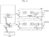
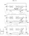
- FIG. 13 and FIG. 14 are diagrams showing change in set states of switches included in data drivers according to operation modes of the data driver.
- the first data driver DIC1 may operate in the display mode or the bypass mode according to an EPI signal.
- the first and second data drivers DIC1 and DIC2 may operate in the display mode or the bypass mode according to an EPI signal.
- a high-level checking voltage HV is applied to the connection checking terminal Cin of the third data driver DIC3.
- the high-level checking voltage HV is transferred to the timing controller TCON through the connection checking terminals Cin and Cout of the data drivers DIC1 and DIC2.
- the timing controller TCON may determine whether the data drivers DIC1, DIC2, and DIC3 are normally connected by checking the high-level checking voltage HV.
- FIG. 15 is a diagram showing an example of realizing the bypass mode and the display mode according to control data of a data transmission packet.
- a data transmission packet transmitted from the timing controller TCON to the data driver DIC of each display unit includes control data CTR along with unit image data.
- the control data CTR includes ID information, gate timing information GIP, and the like.
- the data driver DIC of each display unit determines if the ID information included in the control data CTR corresponds thereto by analyzing the ID information.
- the data driver DIC of each display unit operates in the display mode only when the ID information corresponds thereto and operates in the bypass mode if not. For example, when the ID information indicates the third data driver DIC3, the first and second data drivers DIC1 and DIC2 bypass the EPI signal (i.e., the data transmission packet) from the timing controller TCON such that the EPI signal is transferred to the third data driver DIC3.
- the third data driver DIC3 converts the unit image data into a data voltage Vdata and writes the data voltage Vdata into the corresponding display panel in association with the gate timing information GIP.
- FIG. 16 and FIG. 17 are diagrams showing an example of realizing the bypass mode and the sensing mode according to control data of a data transmission packet.
- a data transmission packet transmitted from timing controller TCON to the data driver DIC of each display unit includes control data CTR along with unit image data.
- the control data CTR further includes a sensing enable signal and a target sensing line signal in addition to ID information and gate timing information GIP.
- the data driver DIC of each display unit determines if the ID information included in the control data CTR corresponds thereto by analyzing the ID information.
- the data driver DIC of each display unit operates in the display mode or the sensing mode only when the ID information corresponds thereto and operates in the bypass mode if not. For example, when the ID information indicates the third data driver DIC3, the first and second data drivers DIC1 and DIC2 bypass the EPI signal (i.e., the data transmission packet) from the timing controller TCON such that the EPI signal is transferred to the third data driver DIC3.
- the third data driver DIC3 converts the unit image data into a data voltage Vdata and applies the data voltage Vdata to the corresponding display panel in association with the gate timing information GIP.
- the third data driver DIC3 senses driving characteristics of pixels corresponding to a target sensing line to obtain sensing result data and then feeds back a data transmission packet including this sensing result data to the timing controller TCON.
- the data transmission packet including the sensing result data becomes an EPI feedback signal.
- the EPI feedback signal is fed back to the timing controller TCON via the first and second data drivers DIC1 and DIC2.
- the present embodiment has the following advantages.
- operations of display units are controlled by the timing controller through bidirectional communication.
- the timing controller can control the data driver of each display unit to switch to the feedback switching state or the bypass switching state using set information included in an EPI signal. Since each data driver can bidirectionally transmit an EPI signal and an EPI feedback signal through a bidirectional communication cable, a connection structure of display units is simplified and an additional data processing operation for image synchronization is not required.
Landscapes
- Engineering & Computer Science (AREA)
- Physics & Mathematics (AREA)
- General Physics & Mathematics (AREA)
- Theoretical Computer Science (AREA)
- Computer Hardware Design (AREA)
- Multimedia (AREA)
- Control Of Indicators Other Than Cathode Ray Tubes (AREA)
- Devices For Indicating Variable Information By Combining Individual Elements (AREA)
Abstract
Description
- This application claims the benefit of
Korean Patent Application No. 10-2020-0179610, filed on December 21, 2020 - The present disclosure relates to an infinitely expandable display device having expandability.
- Recently, large displays have been used in various fields such as indoor and outdoor digital advertisements. To meet the demand for large displays, a display device having expandability is proposed. An infinitely expandable display device forms a screen by connecting a plurality of display units and has the advantage that the screen size can be increased as necessary.
- However, each display unit of an infinitely expandable display device includes a control printed circuit board and an application-specific integrated circuit mounted thereon, and thus a connection structure of display units is complicated and an additional data processing operation for image synchronization is required.
- Accordingly, the present disclosure provides an infinitely expandable display device capable of simplifying a connection structure of display units and a data processing operation. An invention is set out in the independent claims.
- An infinitely expandable display device according to the present disclosure includes a plurality of display units including a plurality of data drivers connected through a bidirectional interface circuit, and a timing controller commonly connected to the display units through the bidirectional interface circuit. Each of the data drivers includes a first reception circuit EPI RX configured to receive a first interface signal in a first direction, a first transmission circuit EPI TX configured to transmit the first interface signal in the first direction, a second reception circuit RBUF configured to receive a second interface signal in a second direction opposite the first direction, a second transmission circuit TBUF configured to transmit the second interface signal in the second direction, and a switch circuit SWP connected to the first transmission circuit EPI TX, the second transmission circuit TBUF, and the second reception circuit RBUF.
-
-
FIG. 1 is a diagram schematically showing an infinitely expandable display device according to an embodiment of the present disclosure. -
FIG. 2 is a diagram showing exemplary resolution according to a driving unit of the infinitely expandable display device shown inFIG. 1 . -
FIG. 3 is a diagram showing a configuration of a display unit in the infinitely expandable display device. -
FIG. 4 is a diagram showing that data drivers of display units are commonly connected to a single control printed circuit board. -
FIG. 5 is a diagram showing a configuration of connection between data drivers and peripheral circuits in display units. -
FIG. 6 is a diagram showing a configuration of connection between a timing controller and display units through connection cables. -
FIG. 7 is a diagram showing an internal configuration of a data driver for bidirectional communication. -
FIG. 8 is a diagram showing a configuration of connection between the data driver and the source printed circuit board for bidirectional communication. -
FIG. 9 is a diagram showing operation modes of the data driver. -
FIG. 10 to FIG. 12 are diagrams for describing a control procedure of the timing controller in a set mode ofFIG. 9 . -
FIG. 13 andFIG. 14 are diagrams showing change in set states of switches included in data drivers according to operation modes of the data driver. -
FIG. 15 is a diagram showing an example of realizing a bypass mode and a display mode according to control data of a data transmission packet. -
FIG. 16 andFIG. 17 are diagrams showing an example of realizing the bypass mode and a sensing mode according to control data of a data transmission packet. - The advantages and features of the present disclosure and the way of attaining the same will become apparent with reference to embodiments described below in detail in conjunction with the accompanying drawings. The present disclosure, however, is not limited to the embodiments disclosed hereinafter and may be embodied in many different forms. Rather, these exemplary embodiments are provided so that this disclosure will be through and complete and will fully convey the scope to those skilled in the art. Thus, the scope of the present disclosure should be defined by the claims.
- The shapes, sizes, ratios, angles, numbers, and the like, which are illustrated in the drawings in order to describe embodiments of the present disclosure, are merely given by way of example, and therefore, the present disclosure is not limited to the illustrations in the drawings. The same elements are designated by the same reference numerals throughout the specification. In the present disclosure, when the terms "comprise", "include", and the like are used, other elements may be added unless the term "only" is used. An element described in the singular form is intended to include a plurality of elements unless the context clearly indicates otherwise.
- In the interpretation of constituent elements included in the various embodiments of the present disclosure, the constituent elements are interpreted as including an error range even if there is no explicit description thereof.
- When describing positional relationships, for example, when the positional relationship between two parts is described using "on", "above", "below", "beside", or the like, one or more other parts may be located between the two parts unless the term "directly" or "closely" is used.
- In the description of the various embodiments of the present disclosure, although terms such as "first" and "second" may be used to describe various elements, these terms are merely used to distinguish the same or similar elements from each other. Therefore, in the present disclosure, an element modified by "first" may be the same as an element modified by "second" within the technical scope of the present disclosure unless otherwise mentioned.
- Hereinafter, embodiments of the present disclosure will be described in detail with reference to the attached drawings. In the following description, if a detailed description of known techniques associated with the present disclosure would unnecessarily obscure the gist of the present disclosure, detailed description thereof will be omitted.
-
FIG. 1 is a diagram schematically showing an infinitely expandable display device according to an embodiment of the present disclosure.FIG. 2 is a diagram showing an exemplary resolution according to a driving unit of the infinitely expandable display device shown inFIG. 1 .FIG. 3 is a diagram showing a configuration of a display unit in the infinitely expandable display device.FIG. 4 is a diagram showing that data drivers of display units are commonly connected to a single control printed circuit board.FIG. 5 is a diagram showing a configuration of connection between a data driver and peripheral circuits in a display unit.FIG. 6 is a diagram showing a configuration of connection between a timing controller and display units through connection cables. As used herein, references to an infinitely expandable display device may be used to indicate that it is possible to connect further display units to an existing plurality of display units of the display device, for example in a modular manner, in order to expand the display area of the display device. As used herein, references to a timing controller being commonly connected to the display units through a bidirectional interface circuit may refer to the timing controller being connected to all of, or at least to a plurality of, the display units, or to the data drivers thereof, through the bidirectional interface circuit. - Referring to
FIG. 1 , the infinitely expandable display device according to an embodiment of the present disclosure includes a set board and a cabinet. - The cabinet includes a plurality of display units connected through a bidirectional interface circuit to construct a screen. The full resolution of the large screen is determined by the sum of unit resolutions of the display units. For example, if the cabinet is composed of 16 display units having a unit resolution of 480*270, as shown in
FIG. 2 , the full resolution of the cabinet is 1920*1080. - The display units may be implemented as an electroluminescent display type capable of sensing driving characteristics of pixels. However, the technical spirit of the present disclosure is not limited to the method of implementing the display units.
- A gap (i.e., seam size) between the display units is designed to be less than a gap between pixels (i.e., pixel pitch) in order to achieve zero bezel. The zero bezel improves visibility and readability of the screen.
- The display units are connected through a cascading internal interface circuit to sequentially transfer image data generated in the set board. Each display unit corresponds to an electroluminescent display device including a display panel in which pixels are formed and a panel driving circuit for driving the display panel. The panel driving circuit includes a data driver and a gate driver.
- A pixel array as shown in
FIG. 3 is formed on the front side of the display panel. The pixel array may include a plurality of sub-pixels and signal lines for supplying a driving voltage to the plurality of sub-pixels. These signal lines may include data lines DL for transmitting data voltages Vdata, gate lines GL1 and GL2 for transmitting gate signals SCAN and SEN, and readout lines RL for supplying a reference voltage VREF and sensing pixel driving characteristics Vsen. In addition, the signal lines disposed in the pixel array may further include a driving voltage line for transmitting a high-level pixel voltage EVDD. The data lines DL and the readout lines RL may extend in a first direction on the pixel array and the gate lines GL1 and GL2 may extend in a second direction perpendicular to the first direction. These signal lines may be connected to a pixel circuit of each sub-pixel and connected to the panel driving circuit. A low-level pixel voltage EVSS may be supplied to the pixel array. Here, the low-level pixel voltage EVSS may be a common voltage applied to all sub-pixels. The low-level pixel voltage EVSS may be applied as a higher voltage in a sensing mode for driving characteristic detection than in a display mode for image writing, but the present disclosure is not limited thereto. - A plurality of sub-pixels may constitute a single pixel. For example, R (red), W (white), G (green), and B (blue) sub-pixels neighboring in the first direction may constitute a single pixel. However, R, G, and B sub-pixels may constitute a single pixel. In this case, W sub-pixels may be omitted from the pixel array. R, W, G, and B sub-pixels have the same pixel circuit configuration although they have different luminescent materials forming light-emitting elements.
- A sub-pixel may include a light-emitting element OLED, a driving TFT DT, switching TFTs ST1 and ST2, and a storage capacitor Cst, as shown in
FIG. 3 . The driving TFT DT and the switching TFTs ST1 and ST2 may be implemented as NMOSs, but the present disclosure is not limited thereto. - The light-emitting element OLED emits light with intensity corresponding to pixel current input from the driving TFT DT. The light-emitting element OLED may be implemented as an organic light-emitting diode including an organic emission layer or an inorganic light-emitting diode including an inorganic emission layer. An anode of the light-emitting element OLED is connected to a second node N2 and a cathode thereof is connected to an input terminal to which the low-level pixel voltage EVSS is applied.
- The driving TFT DT is a driving element that generates pixel current corresponding to a gate-source voltage. A gate electrode of the driving TFT DT is connected to a first node N1, a first electrode (drain electrode) thereof is connected to an input terminal to which the high-level pixel voltage EVDD is applied, and a second electrode (source electrode) thereof is connected to the second node N2.
- The switching TFTs ST1 and ST2 are switching elements that set the gate-source voltage of the driving TFT DT and connect the second electrode of the driving TFT DT to the readout lines RL.
- The first switching TFT ST1 is connected between a data line DL and the first node N1 and is turned on according to the first gate signal SCAN from the first gate line GL1. The first switching TFT ST1 is turned on during programming in the display mode and the sensing mode. When the first switching TFT ST1 is turned on, a data voltage Vdata for display or sensing is applied to the first node N1. The gate electrode of the first switching TFT ST1 is connected to the first gate line GL1, the first electrode thereof is connected to the data line DL, and the second electrode thereof is connected to the first node N1.
- The second switching TFT ST2 is connected between a readout line RL and the second node N2 and is turned on according to the second gate signal SEN from the second gate line GL2. The second switching TFT ST2 is turned on during programming in the display mode and the sensing mode to apply the reference voltage VREF to the second node N2. In addition, the second switching TFT ST2 is also turned on during a sensing operation after set-up in the sensing mode to transfer a source node voltage (or a source voltage) of the driving TFT DT to the readout line RL. Then, a sensing voltage Vsen corresponding to the source voltage is stored in a parasitic capacitor Cp of the readout line RL. The gate electrode of the second switching TFT ST2 is connected to the second gate line GL2, the first electrode thereof is connected to the readout line RL, and the second electrode thereof is connected to the second node N2.
- The storage capacitor Cst is connected between the first node N1 and the second node N2 and maintains the gate-source voltage of the driving TFT DT for a predetermined time. The gate-source voltage of the driving TFT DT is programmed to a difference voltage between the data voltage Vdata for display and the reference voltage VREF in the display mode and is programmed to a difference voltage between the data voltage Vdata for sensing and the reference voltage VREF in the sensing mode.
- In the display mode, pixel current corresponding to the gate-source voltage of the driving TFT DT flows through the driving TFT DT and thus the light-emitting element OLED emits light according to the pixel current. In the sensing mode, pixel current corresponding to the gate-source voltage of the driving TFT DT flows through the driving TFT DT and thus a source node voltage of the driving TFT DT changes according to the pixel current. Since the source node voltage changes according to driving characteristics of the driving TFT DT, change in the driving characteristics of the driving TFT DT may be detected through a sensing voltage Vsen corresponding to the source node voltage. Meanwhile, the low-level pixel voltage EVSS is applied as a voltage higher than the operating point voltage of the light-emitting element OLED in the sensing mode, and thus the pixel current of the driving TFT DT does not flow to the light-emitting element OLED and flows only through the readout line RL. Accordingly, sensing reliability can be improved because the source node voltage is reflected in the sensing voltage Vsen within a short time.
- Such a sub-pixel configuration and operation are merely an example and thus the technical spirit of the present disclosure is not limited thereto. For example, the first and second gate signals SCAN and SEN may be unified and the first and second gate lines GL1 and GL2 may be unified. Further, the sub-pixel configuration may be modified to be suitable for double rate driving.
- As shown in
FIG. 4 , each display unit does not individually include an application specific integrated circuit (ASIC). In addition, operations of the display units are controlled by a single timing controller TCON through bidirectional communication. Accordingly, a connection structure of the display units is simplified and an additional data processing operation for image synchronization is not required. - Referring to
FIG. 4 , the display units include a plurality of data drivers DIC connected through a bidirectional interface circuit. The timing controller TCON is mounted on a control printed circuit board C-PCB and is connected to the data drivers DIC through a bidirectional interface circuit. The bidirectional interface circuits may be connected through a bidirectional communication cable. In addition, the bidirectional interface circuits may be implemented as an embedded panel interface (EPI). - The data drivers DIC may be positioned on the backside of a display panel, as shown in
FIG. 5 . A source printed circuit board S-PCB is additionally positioned on the backside of the display unit. A conductive film COF in which the data driver DIC is mounted is bonded to the source printed circuit board S-PCB. The source printed circuit board S-PCB includes a first connection terminal CTX and a second connection terminal CRX to be connected to a bidirectional communication cable CBL, as shown inFIG. 6 . Further, the control printed circuit board C-PCB also includes the first connection terminal CTX and the second connection terminal CRX to be connected to the bidirectional communication cable CBL. Accordingly, the timing controller TCON is electrically connected to the data drivers DIC, and a first interface signal (hereinafter, an EPI signal) in a first direction and a second interface signal (hereinafter, an EPI feedback signal) in a second direction that is the opposite direction to the first direction are transmitted and received between the data drivers DIC and the timing controller TCON electrically connected to it. As used herein, references to receiving/transmitting signals in a given direction (e.g. a first/second direction) may refer to directions in the plane of the surface of the expandable display device, i.e. in the plane of the display area. Therefore, references to receiving/transmitting signals in first/second directions may refer to receiving/transmitting signals from/to adjacent display units. For a grid of display units, the first/second directions may point along a column of the display units (e.g. in the 'up-down' direction as shown inFIG. 1 ). For example, the first direction may point upwards towards the top of the display and the second direction may point downwards towards the bottom of the display. Alternatively, the first direction may point downwards towards the bottom of the display and the second direction may point upwards towards the top of the display. For a grid of display units, the first/second directions may point along a row of the display units (e.g. in the left-right' direction as shown inFIG. 1 ). For example, the first direction may point rightwards towards the right edge of the display and the second direction may point leftwards towards the left edge of the display. Alternatively, the first direction may point leftwards towards the left of the display and the second direction may point rightwards towards the right of the display. Other orientations, directions, and arrangements of display units are possible and considered within the present disclosure. As used herein, references to a second direction being opposite a first direction may be used to indicate that, whereas transmitting a signal in a first direction may comprise transmitting a signal from a first display unit to a second display unit, receiving a signal in the second direction may comprise receiving a signal from the second display unit at the first display unit. - The data driver DIC includes a digital-to-analog converter DAC that generates a data voltage Vdata, a sensing circuit SENU, and an analog-to-digital converter ADC. The digital-to-analog converter DAC converts image data supplied from the timing controller TCON into the data voltage Vdata for display according to a timing control signal and then provides the data voltage Vdata to the data lines DL in the display mode. The digital-to-analog converter DAC generates the data voltage Vdata for sensing and then provides the data voltage Vdata for sensing to the data lines DL in the sensing mode.
- The sensing circuit SENU provides the reference voltage VREF to the readout lines RL in the display mode. The sensing circuit SENU provides the reference voltage VREF to the readout lines RL and then samples a sensing voltage Vsen charged in the readout lines RL in the sensing mode. The sensing circuit SENU includes a reference voltage switch SPRE connected between the readout line RL and a reference voltage VREF input terminal, and a sampling switch SAM connected between the readout line RL and the analog-to-digital converter ADC. The reference voltage switch SPRE is turned on only in a programming period of the display mode and the sensing mode and the sampling switch SAM is turned on only in a sampling period of the sensing mode.
- The analog-to-digital converter ADC performs digital processing on a sampling voltage generated when the sampling switch SAM is turned on to output sensing result data SDATA in the sensing mode. The sensing result data SDATA may be a signal representing a result of execution according to a driving command signal.
- The gate driver may receive an operation voltage and a timing control signal through the data driver DIC. The gate driver may be embedded in a non-display area around the pixel array of the display panel. The gate driver generates the first and second gate signals SCAN and SEN according to the timing control signal and provides the first and second gate signals SCAN and SEN to the first and second gate lines GL1 and GL2. The first and second gate signals SCAN and SEN are used to select a pixel line in which the data voltage Vdata for display will be written in the display mode and used to select a sensing target pixel line in the sensing mode. Here, a pixel line refers to a set of pixels and signal lines neighboring in the second direction.
-
FIG. 7 is a diagram showing an internal configuration of the data driver for bidirectional communication andFIG. 8 is a diagram showing a configuration of connection between the data driver and the source printed circuit board for bidirectional communication. - Referring to
FIG. 7 andFIG. 8 , each data driver DIC receives an EPI signal from the timing controller TCON or a preceding data driver DIC adjacent thereto and transfers the EPI signal to a following data driver DIC adjacent thereto. The EPI signal is transferred to the data drivers DIC connected through the bidirectional interface circuit. The EPI signal may include unit image data to be written in each display unit, a sensing command signal, an ID command signal, and the like. - Each data driver DIC receives an EPI feedback signal from the following data driver DIC adjacent thereto and transfers the EPI feedback signal to the preceding data driver DIC adjacent thereto. The EPI feedback signal is fed back from at least one data driver DIC to the timing controller TCON through the bidirectional interface circuit. The EPI feedback signal may include sensing result data SDATA corresponding to the sensing command signal, an ID allocation completion signal corresponding to the ID command signal, and the like.
- Each data driver DIC may include a first reception circuit EPI RX, a first transmission circuit EPI TX, a second reception circuit RBUF, a second transmission circuit TBUF, and a switch circuit SWP.
- The first reception circuit EPI RX receives an EPI signal from the timing controller TCON or a preceding data driver DIC adjacent thereto. The first transmission circuit EPI TX transmits the EPI signal to a following data driver DIC adjacent thereto. The second reception circuit RBUF receives an EPI feedback signal from the following driver DIC adjacent thereto. The second transmission circuit EPI TBUF transmits the EPI feedback signal to the preceding data driver DIC adjacent thereto. In addition, the switch circuit SWP is connected to the first transmission circuit EPI TX, the second transmission circuit TBUF, and the second reception circuit RBUF and switches to a bypass switching state or a feedback switching state according to switch set information included in the EPI signal. The bypass switching state and the feedback switching state differ from each other. Further, the second reception circuit RBUF and the second transmission circuit TBUF also serve to store the EPI feedback signal for a predetermined time and to remove noise to stabilize the signal.
- The data driver DIC may further include a first signal terminal Ta connected to the first reception circuit EPI RX, a second signal terminal Tb connected to the first transmission circuit EPI TX, a third signal terminal Tc connected to the second reception circuit RBUF, and a fourth signal terminal Td connected to the second transmission circuit TBUF.
- The first signal terminal Ta and the fourth signal terminal Td are connected to a first bidirectional communication cable CBL through a second connection terminal CRX of a source printed circuit board S-PCB. The first bidirectional communication cable CBL is connected to a first connection terminal CTX of a preceding source printed circuit board S-PCB.
- The second signal terminal Tb and the third signal terminal Tc are connected to a second bidirectional communication cable CBL through the first connection terminal CTX of the source printed circuit board S-PCB. The second bidirectional communication cable CBL is connected to the second connection terminal CRX of a following source printed circuit board S-PCB.
- According to the configuration of connection for bidirectional communication, as shown in
FIG. 7 andFIG. 8 , the advantage of simplifying the internal configuration of the data driver can be obtained because the EPI signal and the EPI feedback signal can be bidirectionally transmitted through the bidirectional communication cable CBL. - In
FIG. 8 , Cin and Cout represent connection checking terminals for checking connection between data drivers in a set mode for assigning identification numbers ID to display units. This will be described later in description ofFIG. 10 to FIG. 12 . -
FIG. 9 is a diagram showing operation modes of the data driver. - Referring to
FIG. 9 , the data driver may operate in any one of an idle mode, the set mode, a bypass mode, the display mode, and the sensing mode. - The idle mode is a driving mode corresponding to an initial state immediately after application of system power (or main driving power). The set mode is a driving mode for ID allocation (i.e., assignment identification numbers). The bypass mode is a driving mode for bypassing a received EPI signal or EPI feedback signal to the following data driver when the EPI signal or the EPI feedback signal does not match an allocated ID. The display mode is a driving mode for converting unit image data into a data voltage and applying the data voltage to the display panel when a received EPI signal matches the allocated ID. The sensing mode is a driving mode for sensing driving characteristics of pixels corresponding to a sensing command signal and generating sensing result data SDATA when a received EPI signal matches the allocated ID.
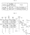
- The switch circuit SWP included in the data driver switches to the bypass switching state (refer to "SW_SET=101" in
FIG. 10 ) or switches to the feedback switching state (refer to "SW_SET=010" inFIG. 10 ) according to the set mode, the bypass mode, the display mode, or the sensing mode. In the idle mode, the switch circuit SWP switches to an initial switching state (for example, "SW_SET=000"). -
FIG. 10 to FIG. 12 are diagrams for describing a control procedure of the timing controller in the set mode ofFIG. 9 . - Referring to
FIG. 10 to FIG. 12 , when system power is applied, the timing controller TCON monitors the connection checking terminals Cin and Cout of the data driver DIC to check connection between data drivers to which IDs need to be allocated (S11 and S12). - Upon confirmation of connection between the data drivers, the timing controller TCON includes an ID set enable signal (i.e., ID command signal) in an EPI signal and transmits the EPI signal to a first data driver DIC1 to which ID=1 will be allocated (S13, S14, and S15).
- The first data driver DIC1 switches from the idle mode to the set mode according to the ID command signal and sets ID=1. Then, the first data driver DIC1 switches the switch circuit SWP to the feedback switching state ("SW_SET=010") and feeds back an ID allocation completion signal to the timing controller TCON (S16 and S17).
- The timing controller TCON checks the feedback signal, includes a bypass mode enable signal in the EPI signal and transmits the EPI signal to the first data driver DIC1 (S18).
- The first data driver DIC1 switches from the set mode to the bypass mode according to the bypass mode enable signal and switches the switch circuit SWP to the bypass switching state ("SW_SET=101") (S19).
- The timing controller TCON includes an ID command signal in an EPI signal and transmits the EPI signal to a second data driver DIC2 to which ID=2 will be allocated (S20). This ID command signal is transmitted to the second data driver DIC2 through the first data driver DIC1 in the bypass switching state ("SW_SET=101").
- The second data driver DIC2 switches from the idle mode to the set mode according to the ID command signal and sets ID=2. Then, the second data driver DIC2 switches the switch circuit SWP to the feedback switching state ("SW_SET=010") and feeds back an ID allocation completion signal to the timing controller TCON. The ID allocation completion signal is fed back to the timing controller TCON through the first data driver DIC1 in the bypass switching state ("SW_SET=101").
- The timing controller TCON checks the feedback signal, includes the bypass mode enable signal in the EPI signal and transmits the EPI signal to the second data driver DIC2. The bypass mode enable signal is transmitted to the second data driver DIC2 through the first data driver DIC1 in the bypass switching state ("SW_SET=101").
- The second data driver DIC2 switches from the set mode to the bypass mode according to the bypass mode enable signal and switches the switch circuit SWP to the bypass switching state ("SW_SET=101").
- In this manner, the timing controller TCON assigns IDs to data drivers DIC1 to DIC3 to which IDs need to be allocated, checks the ID allocation completion signal, and then switches the switch circuit SWP included in each of the data drivers DIC1 to DIC3 to the bypass switching state ("SW_SET=101") (S21 and S22).
- Here, when the switch circuit SWP in the feedback switching state ("SW_SET=010") or the bypass switching state ("SW_SET=101") is used, the advantage of considerably reducing the number of cables necessary to signal transmission/feedback is obtained.
- Referring to
FIG. 11 , the switch circuit SWP may include a first switch SW1 connected between the first transmission circuit EPI TX and the second signal terminal Tb, a second switch SW2 connected between the first transmission circuit EPI TX and the second transmission circuit TBUF, and a third switch SW3 connected between the second transmission circuit TBUF and the second reception circuit RBUF. - In this switch circuit SWP, the first switch SW1 and the third switch SW3 are turned on/off in the same manner and the second switch SW2 is turned on/off reversely to the first and third switches SW1 and SW3 to implement the feedback switching state ("SW_SET=010") and the bypass switching state ("SW_SET=101").
- The feedback switching state ("SW_SET=010") and the bypass switching state ("SW_SET=101") are results of combinations of on/off states of the switches SW1, SW2, and SW3 included in the switch circuit SWP. The first switch SW1 and the third switch SW3 are turned on and the second switch SW2 is turned off in the bypass switching state ("SW_SET=101"). The first switch SW1 and the third switch SW3 are turned off and the second switch SW2 is turned on in the feedback switching state ("SW_SET=010").
- The feedback switching state ("SW_SET=010") and the bypass switching state ("SW_SET=101") are determined according to switch set information. The switch set information may be included in control data in a data transmission packet constituting an EPI signal. Such switch set information may be independently set for each data driver.
- The timing controller TCON may sequentially drive the display units in the set mode based on switch set information to assign different identification numbers (nID = 1, 2, and 3) to the display units.
-
FIG. 13 andFIG. 14 are diagrams showing change in set states of switches included in data drivers according to operation modes of the data driver. - Referring to
FIG. 13 , when the second data driver DIC2 operates in the set mode or the sensing mode, the switch circuit SWP of the second data driver DIC2 switches to the feedback switching state ("SW_SET=010") and the switch circuit SWP of the first data driver DIC1 switches to the bypass switching state ("SW_SET=101"). In the feedback switching state, SW1=0 (off), SW2=1 (on), and SW3=0 (off). In the bypass switching state, SW1=0 (on), SW2=1 (off), and SW3=0 (on). Here, the first data driver DIC1 may operate in the display mode or the bypass mode according to an EPI signal. - Referring to
FIG. 14 , when the third data driver DIC3 operates in the set mode or the sensing mode, the switch circuit SWP of the third data driver DIC3 switches to the feedback switching state ("SW_SET=010") and the switch circuits SWP of the first and second data drivers DIC1 and DIC2 switch to the bypass switching state ("SW_SET=101"). In the feedback switching state, SW1=0 (off), SW2=1 (on), and SW3=0 (off). In the bypass switching state, SW1=0 (on), SW2=1 (off), and SW3=0 (on). Here, the first and second data drivers DIC1 and DIC2 may operate in the display mode or the bypass mode according to an EPI signal. - Meanwhile, a high-level checking voltage HV is applied to the connection checking terminal Cin of the third data driver DIC3. The high-level checking voltage HV is transferred to the timing controller TCON through the connection checking terminals Cin and Cout of the data drivers DIC1 and DIC2. The timing controller TCON may determine whether the data drivers DIC1, DIC2, and DIC3 are normally connected by checking the high-level checking voltage HV.
-
FIG. 15 is a diagram showing an example of realizing the bypass mode and the display mode according to control data of a data transmission packet. - Referring to
FIG. 15 , a data transmission packet transmitted from the timing controller TCON to the data driver DIC of each display unit includes control data CTR along with unit image data. The control data CTR includes ID information, gate timing information GIP, and the like. - The data driver DIC of each display unit determines if the ID information included in the control data CTR corresponds thereto by analyzing the ID information. The data driver DIC of each display unit operates in the display mode only when the ID information corresponds thereto and operates in the bypass mode if not. For example, when the ID information indicates the third data driver DIC3, the first and second data drivers DIC1 and DIC2 bypass the EPI signal (i.e., the data transmission packet) from the timing controller TCON such that the EPI signal is transferred to the third data driver DIC3. The third data driver DIC3 converts the unit image data into a data voltage Vdata and writes the data voltage Vdata into the corresponding display panel in association with the gate timing information GIP.
-
FIG. 16 andFIG. 17 are diagrams showing an example of realizing the bypass mode and the sensing mode according to control data of a data transmission packet. - Referring to
FIG. 16 andFIG. 17 , a data transmission packet transmitted from timing controller TCON to the data driver DIC of each display unit includes control data CTR along with unit image data. The control data CTR further includes a sensing enable signal and a target sensing line signal in addition to ID information and gate timing information GIP. - The data driver DIC of each display unit determines if the ID information included in the control data CTR corresponds thereto by analyzing the ID information. The data driver DIC of each display unit operates in the display mode or the sensing mode only when the ID information corresponds thereto and operates in the bypass mode if not. For example, when the ID information indicates the third data driver DIC3, the first and second data drivers DIC1 and DIC2 bypass the EPI signal (i.e., the data transmission packet) from the timing controller TCON such that the EPI signal is transferred to the third data driver DIC3. The third data driver DIC3 converts the unit image data into a data voltage Vdata and applies the data voltage Vdata to the corresponding display panel in association with the gate timing information GIP. In addition, the third data driver DIC3 senses driving characteristics of pixels corresponding to a target sensing line to obtain sensing result data and then feeds back a data transmission packet including this sensing result data to the timing controller TCON. The data transmission packet including the sensing result data becomes an EPI feedback signal. The EPI feedback signal is fed back to the timing controller TCON via the first and second data drivers DIC1 and DIC2.
- The present embodiment has the following advantages.
- According to the infinitely expandable display device according to embodiments of the present disclosure, operations of display units are controlled by the timing controller through bidirectional communication. The timing controller can control the data driver of each display unit to switch to the feedback switching state or the bypass switching state using set information included in an EPI signal. Since each data driver can bidirectionally transmit an EPI signal and an EPI feedback signal through a bidirectional communication cable, a connection structure of display units is simplified and an additional data processing operation for image synchronization is not required.
- It will be appreciated by persons skilled in the art that the effects that can be achieved with the present disclosure are not limited to what has been particularly described hereinabove and other advantages of the present disclosure will be more clearly understood from the following detailed description.
- Those skilled in the art will appreciate that various modifications and variations can be made in the present disclose without departing from the spirit or scope of the invention. Accordingly, the scope of the present disclosure should be determined by the appended claims and their legal equivalents, not by the above description. The disclosure comprises the following items:
- 1. An infinitely expandable display device, comprising:
- a plurality of display units including a plurality of data drivers connected through a bidirectional interface circuit; and
- a timing controller commonly connected to the display units through the bidirectional interface circuit,
- wherein each of the data drivers includes:
- a first reception circuit EPI RX configured to receive a first interface signal in a first direction;
- a first transmission circuit EPI TX configured to transmit the first interface signal in the first direction;
- a second reception circuit RBUF configured to receive a second interface signal in a second direction opposite the first direction;
- a second transmission circuit TBUF configured to transmit the second interface signal in the second direction; and
- a switch circuit SWP connected to the first transmission circuit EPI TX, the second transmission circuit TBUF, and the second reception circuit RBUF.
- 2. The infinitely expandable display device of
item 1, wherein each of the data drivers includes:- a first signal terminal Ta connected to the first reception circuit;
- a second signal terminal Tb connected to the first transmission circuit;
- a third signal terminal Tc connected to the second reception circuit; and
- a fourth signal terminal Td connected to the second transmission circuit.
- 3. The infinitely expandable display device of
item 2, wherein the switch circuit SWP includes:- a first switch SW1 connected between the first transmission circuit EPI TX and the second signal terminal Tb;
- a second switch SW2 connected between the first transmission circuit EPI TX and the second transmission circuit TBUF; and
- a third switch SW3 connected between the second transmission circuit TBUF and the second reception circuit RBUF.
- 4. The infinitely expandable display device of
item 3, wherein the first switch SW1 and the third switch SW3 are turned on/off in the same manner and the second switch SW2 and the second switch SW2 is turned on/off reversely to the first and third switches SW1 and SW3. - 5. The infinitely expandable display device of
item 3, wherein the first switch SW1 and the third switch SW3 are turned off and the second switch SW2 is turned on in a feedback switching state, and the first switch SW1 and the third switch SW3 are turned on and the second switch SW2 is turned off in a bypass switching state. - 6. The infinitely expandable display device of item 5, wherein the bypass switching state or the feedback switching state is determined according to switch set information, and the switch set information is included in control data in a data transmission packet constituting the first interface signal in the first direction.
- 7. The infinitely expandable display device of item 6, wherein the switch set information is independently set for each of the data drivers.
- 8. The infinitely expandable display device of item 6 or item 7, wherein the timing controller sequentially drives the display units in a set mode based on the switch set information to assign different identification numbers to the display units.
- 9. The infinitely expandable display device of any of items 6-8, wherein the timing controller drives at least any one of the display units in a sensing mode based on the switch set information to obtain sensing information of a corresponding pixel line.
- 10. The infinitely expandable display device of item 9, wherein the sensing information of the corresponding pixel line is included in a data transmission packet constituting the second interface signal in the second direction and fed back to the timing controller.
- 11. The infinitely expandable display device of any preceding item, wherein the bidirectional interface circuit is connected through a bidirectional communication cable.
- 12. The infinitely expandable display device of any preceding item, wherein the first interface signal in the first direction and the second interface signal in the second direction are implemented by an embedded panel interface (EPI).
- 13. The infinitely expandable display device of
item 12, wherein the first interface signal in the first direction is an EPI signal including unit image data to be written into each display unit, a sensing command signal, and an ID command signal, and the second interface signal in the second direction is an EPI feedback signal including sensing result data corresponding to the sensing command signal, and an ID setting completion signal corresponding to the ID command signal.
Claims (13)
- An expandable display device, comprising:a plurality of display units each including a respective data driver, the data drivers being connected through a bidirectional interface circuit; anda timing controller connected to the display units through the bidirectional interface circuit,wherein each of the data drivers includes:a first reception circuit EPI RX configured to receive a first interface signal in a first direction;a first transmission circuit EPI TX configured to transmit the first interface signal in the first direction;a second reception circuit RBUF configured to receive a second interface signal in a second direction opposite the first direction;a second transmission circuit TBUF configured to transmit the second interface signal in the second direction; anda switch circuit SWP connected to the first transmission circuit EPI TX, the second transmission circuit TBUF, and the second reception circuit RBUF.
- The expandable display device of claim 1, wherein each of the data drivers includes:a first signal terminal Ta connected to the first reception circuit;a second signal terminal Tb connected to the first transmission circuit;a third signal terminal Tc connected to the second reception circuit; anda fourth signal terminal Td connected to the second transmission circuit.
- The expandable display device of claim 2, wherein the switch circuit SWP includes:a first switch SW1 connected between the first transmission circuit EPI TX and the second signal terminal Tb;a second switch SW2 connected between the first transmission circuit EPI TX and the second transmission circuit TBUF; anda third switch SW3 connected between the second transmission circuit TBUF and the second reception circuit RBUF.
- The expandable display device of claim 3, wherein the first switch SW1 and the third switch SW3 are configured to be turned on/off in the same manner and the second switch SW2 and the second switch SW2 is configured to be turned on/off reversely to the first and third switches SW1 and SW3.
- The expandable display device of claim 3, wherein the first switch SW1 and the third switch SW3 are configured to be turned off and the second switch SW2 is configured to be turned on in a feedback switching state, and the first switch SW1 and the third switch SW3 are configured to be turned on and the second switch SW2 is configured to be turned off in a bypass switching state.
- The expandable display device of claim 5, configured to determine the bypass switching state or the feedback switching state according to switch set information, the switch set information being included in control data in a data transmission packet constituting the first interface signal in the first direction.
- The expandable display device of claim 6, wherein the switch set information is independently set for each of the data drivers.
- The expandable display device of claim 6 or claim 7, wherein the timing controller is configured to sequentially drive the display units in a set mode based on the switch set information to assign different identification numbers to the display units.
- The expandable display device of any of claims 6-8, wherein the timing controller is configured to drive at least any one of the display units in a sensing mode based on the switch set information to obtain sensing information of a corresponding pixel line.
- The expandable display device of claim 9, wherein the sensing information of the corresponding pixel line is included in a data transmission packet constituting the second interface signal in the second direction and fed back to the timing controller.
- The expandable display device of any preceding claim, wherein the bidirectional interface circuit is connected through a bidirectional communication cable.
- The expandable display device of any preceding claim, wherein the first interface signal in the first direction and the second interface signal in the second direction are implemented by an embedded panel interface (EPI).
- The expandable display device of claim 12, wherein the first interface signal in the first direction is an EPI signal including unit image data to be written into each display unit, a sensing command signal, and an ID command signal, and the second interface signal in the second direction is an EPI feedback signal including sensing result data corresponding to the sensing command signal, and an ID setting completion signal corresponding to the ID command signal.
Applications Claiming Priority (1)
| Application Number | Priority Date | Filing Date | Title |
|---|---|---|---|
| KR1020200179610A KR102857434B1 (en) | 2020-12-21 | 2020-12-21 | Infinitely Expandable Display Device |
Publications (1)
| Publication Number | Publication Date |
|---|---|
| EP4016278A1 true EP4016278A1 (en) | 2022-06-22 |
Family
ID=78617229
Family Applications (1)
| Application Number | Title | Priority Date | Filing Date |
|---|---|---|---|
| EP21207866.1A Pending EP4016278A1 (en) | 2020-12-21 | 2021-11-11 | Infinitely expandable display device |
Country Status (5)
| Country | Link |
|---|---|
| US (1) | US11495167B2 (en) |
| EP (1) | EP4016278A1 (en) |
| JP (1) | JP7304924B2 (en) |
| KR (1) | KR102857434B1 (en) |
| CN (1) | CN114648961B (en) |
Cited By (1)
| Publication number | Priority date | Publication date | Assignee | Title |
|---|---|---|---|---|
| GB2614369A (en) * | 2021-12-31 | 2023-07-05 | Lg Display Co Ltd | Tiling display apparatus |
Families Citing this family (2)
| Publication number | Priority date | Publication date | Assignee | Title |
|---|---|---|---|---|
| EP4414825A4 (en) * | 2022-04-29 | 2025-03-19 | Samsung Electronics Co., Ltd. | Electronic device for multi-display control |
| US12039917B2 (en) * | 2022-12-02 | 2024-07-16 | X Display Company Technology Limited | Displays with hybrid-control pixel clusters |
Citations (3)
| Publication number | Priority date | Publication date | Assignee | Title |
|---|---|---|---|---|
| US20160019831A1 (en) * | 2014-07-16 | 2016-01-21 | Ultravision Technologies, Llc | Display System having Module Display Panel with Circuitry for Bidirectional Communication |
| US20180006101A1 (en) * | 2016-06-30 | 2018-01-04 | Lg Display Co., Ltd. | Organic light emitting diode display device |
| EP3316241A1 (en) * | 2016-10-31 | 2018-05-02 | LG Display Co., Ltd. | Display device |
Family Cites Families (24)
| Publication number | Priority date | Publication date | Assignee | Title |
|---|---|---|---|---|
| JPS5350607A (en) * | 1976-10-20 | 1978-05-09 | Hitachi Ltd | Loop communication system |
| JP3594856B2 (en) * | 1999-11-12 | 2004-12-02 | パイオニア株式会社 | Active matrix display device |
| TW582015B (en) * | 2000-06-30 | 2004-04-01 | Nichia Corp | Display unit communication system, communication method, display unit, communication circuit and terminal adapter |
| JP4665375B2 (en) * | 2000-07-28 | 2011-04-06 | 日亜化学工業株式会社 | Display device |
| AU2002211116A1 (en) | 2000-10-06 | 2002-04-15 | Virtual Spectator International Limited | Interactive display system |
| JP2002229502A (en) | 2001-01-31 | 2002-08-16 | Nichia Chem Ind Ltd | Display unit communication system and communication method thereof |
| JP2006109258A (en) | 2004-10-07 | 2006-04-20 | Hitachi Ltd | Communication method and communication apparatus |
| JP4364849B2 (en) * | 2004-11-22 | 2009-11-18 | 三星モバイルディスプレイ株式會社 | Luminescent display device |
| KR100728007B1 (en) | 2005-10-26 | 2007-06-14 | 삼성전자주식회사 | Liquid Crystal Display and Driving Method of Liquid Crystal Display |
| US8074581B2 (en) * | 2007-10-12 | 2011-12-13 | Steelcase Inc. | Conference table assembly |
| TWI381715B (en) * | 2008-05-09 | 2013-01-01 | Nexcom Int Co Ltd | A video signal controlling system and method |
| WO2012036133A1 (en) | 2010-09-17 | 2012-03-22 | シャープ株式会社 | Display unit and display device |
| KR20120074517A (en) | 2010-12-28 | 2012-07-06 | 주식회사 오리온 | Apparatus for compensating video signal of multi screen display panel |
| WO2013038554A1 (en) | 2011-09-16 | 2013-03-21 | Necディスプレイソリューションズ株式会社 | Electronic device system |
| KR101845386B1 (en) | 2011-11-22 | 2018-04-05 | 엘지전자 주식회사 | Dispaly device and performaing multi screen |
| TWI460715B (en) * | 2012-02-24 | 2014-11-11 | Aopen Inc | Synchronous and asymmetrical display system and method of operating the same |
| JP2014183482A (en) * | 2013-03-19 | 2014-09-29 | Fujitsu Ltd | Transmission/reception system, transmission device, reception device, and control method for transmission/reception system |
| TWI539431B (en) * | 2014-05-06 | 2016-06-21 | 聯詠科技股份有限公司 | Method for source driving circuit and display device |
| KR102304365B1 (en) * | 2015-02-09 | 2021-09-23 | 엘지전자 주식회사 | Display apparatus and command transmission methods thereof |
| US10860273B2 (en) * | 2015-05-14 | 2020-12-08 | Lg Electronics Inc. | Display device and operation method therefor |
| US9857911B1 (en) * | 2016-07-29 | 2018-01-02 | Parade Technologies, Ltd. | Bi-directional scalable intra-panel interface |
| KR102627278B1 (en) | 2016-09-22 | 2024-01-23 | 엘지디스플레이 주식회사 | Multi-vision system |
| KR102609508B1 (en) * | 2016-11-11 | 2023-12-04 | 엘지디스플레이 주식회사 | Driver Integrated Circuit For External Compensation And Display Device Including The Same |
| WO2018116399A1 (en) * | 2016-12-21 | 2018-06-28 | Necディスプレイソリューションズ株式会社 | Image display device, connection method of image display device, and multi-display system |
-
2020
- 2020-12-21 KR KR1020200179610A patent/KR102857434B1/en active Active
-
2021
- 2021-11-04 CN CN202111299578.8A patent/CN114648961B/en active Active
- 2021-11-04 US US17/519,184 patent/US11495167B2/en active Active
- 2021-11-10 JP JP2021183477A patent/JP7304924B2/en active Active
- 2021-11-11 EP EP21207866.1A patent/EP4016278A1/en active Pending
Patent Citations (3)
| Publication number | Priority date | Publication date | Assignee | Title |
|---|---|---|---|---|
| US20160019831A1 (en) * | 2014-07-16 | 2016-01-21 | Ultravision Technologies, Llc | Display System having Module Display Panel with Circuitry for Bidirectional Communication |
| US20180006101A1 (en) * | 2016-06-30 | 2018-01-04 | Lg Display Co., Ltd. | Organic light emitting diode display device |
| EP3316241A1 (en) * | 2016-10-31 | 2018-05-02 | LG Display Co., Ltd. | Display device |
Cited By (3)
| Publication number | Priority date | Publication date | Assignee | Title |
|---|---|---|---|---|
| GB2614369A (en) * | 2021-12-31 | 2023-07-05 | Lg Display Co Ltd | Tiling display apparatus |
| US11935501B2 (en) | 2021-12-31 | 2024-03-19 | Lg Display Co., Ltd. | Tiling display apparatus |
| US12272333B2 (en) | 2021-12-31 | 2025-04-08 | Lg Display Co., Ltd. | Tiling display apparatus |
Also Published As
| Publication number | Publication date |
|---|---|
| JP7304924B2 (en) | 2023-07-07 |
| JP2022098439A (en) | 2022-07-01 |
| KR20220089197A (en) | 2022-06-28 |
| KR102857434B1 (en) | 2025-09-09 |
| CN114648961A (en) | 2022-06-21 |
| US11495167B2 (en) | 2022-11-08 |
| CN114648961B (en) | 2024-04-09 |
| US20220198993A1 (en) | 2022-06-23 |
Similar Documents
| Publication | Publication Date | Title |
|---|---|---|
| CN114694560B (en) | Light emitting display device and multi-screen light emitting display device including the same | |
| US20240212576A1 (en) | Display device | |
| US11495167B2 (en) | Infinitely expandable display device | |
| EP4116964A1 (en) | Gate driver and display device using the same | |
| KR102745478B1 (en) | Infinitely Expandable Display Device Based On Electroluminescent Display Type And Driving Method Of The Same | |
| CN109979379B (en) | Spliced display and optical compensation method thereof | |
| US10957231B2 (en) | Display apparatus | |
| US20150248855A1 (en) | Organic light emitting display device | |
| KR20200053969A (en) | Display panel and display panel | |
| CN114694620B (en) | Infinitely expandable display device and driving method thereof | |
| US12475852B2 (en) | Pixel circuit, display panel and display device including the same | |
| WO2022068651A1 (en) | Display apparatus, drive chip and electronic device | |
| KR102741512B1 (en) | Display device and mobile terminal device including the same | |
| EP4207169A1 (en) | Gate driver and display device using the same | |
| CN114627838B (en) | Expandable display device and driving method thereof | |
| CN120236515A (en) | Gate driver and display device including the same | |
| CN1933687B (en) | Light-emitting device and method of driving the same | |
| CN118571164A (en) | Display panel and display device | |
| KR102745480B1 (en) | Infinitely Expandable Display Device Based On Electroluminescent Display Type And Driving Method Of The Same | |
| CN100511365C (en) | Method and appts. of driving electroluminiescent display device | |
| KR102626514B1 (en) | Display apparatus | |
| KR20220096041A (en) | Light emitting display apparatus | |
| US20260100160A1 (en) | Display Panel and Display Device Including the Same | |
| US20260080837A1 (en) | Display Device | |
| US20240192801A1 (en) | Sensor device and method for controlling sensor nodes |
Legal Events
| Date | Code | Title | Description |
|---|---|---|---|
| PUAI | Public reference made under article 153(3) epc to a published international application that has entered the european phase |
Free format text: ORIGINAL CODE: 0009012 |
|
| STAA | Information on the status of an ep patent application or granted ep patent |
Free format text: STATUS: REQUEST FOR EXAMINATION WAS MADE |
|
| 17P | Request for examination filed |
Effective date: 20211111 |
|
| AK | Designated contracting states |
Kind code of ref document: A1 Designated state(s): AL AT BE BG CH CY CZ DE DK EE ES FI FR GB GR HR HU IE IS IT LI LT LU LV MC MK MT NL NO PL PT RO RS SE SI SK SM TR |
|
| RBV | Designated contracting states (corrected) |
Designated state(s): AL AT BE BG CH CY CZ DE DK EE ES FI FR GB GR HR HU IE IS IT LI LT LU LV MC MK MT NL NO PL PT RO RS SE SI SK SM TR |
|
| STAA | Information on the status of an ep patent application or granted ep patent |
Free format text: STATUS: EXAMINATION IS IN PROGRESS |
|
| 17Q | First examination report despatched |
Effective date: 20250515 |