EP4016091B1 - Wechselrichtervorrichtung mit einer spannungsmessvorrichtung - Google Patents
Wechselrichtervorrichtung mit einer spannungsmessvorrichtung Download PDFInfo
- Publication number
- EP4016091B1 EP4016091B1 EP21213098.3A EP21213098A EP4016091B1 EP 4016091 B1 EP4016091 B1 EP 4016091B1 EP 21213098 A EP21213098 A EP 21213098A EP 4016091 B1 EP4016091 B1 EP 4016091B1
- Authority
- EP
- European Patent Office
- Prior art keywords
- voltage
- capacitor
- inverter
- switches
- terminals
- Prior art date
- Legal status (The legal status is an assumption and is not a legal conclusion. Google has not performed a legal analysis and makes no representation as to the accuracy of the status listed.)
- Active
Links
Images

Classifications
-
- G—PHYSICS
- G01—MEASURING; TESTING
- G01R—MEASURING ELECTRIC VARIABLES; MEASURING MAGNETIC VARIABLES
- G01R19/00—Arrangements for measuring currents or voltages or for indicating presence or sign thereof
- G01R19/165—Indicating that current or voltage is either above or below a predetermined value or within or outside a predetermined range of values
- G01R19/16533—Indicating that current or voltage is either above or below a predetermined value or within or outside a predetermined range of values characterised by the application
- G01R19/16538—Indicating that current or voltage is either above or below a predetermined value or within or outside a predetermined range of values characterised by the application in AC or DC supplies
- G01R19/16547—Indicating that current or voltage is either above or below a predetermined value or within or outside a predetermined range of values characterised by the application in AC or DC supplies voltage or current in AC supplies
-
- H—ELECTRICITY
- H02—GENERATION; CONVERSION OR DISTRIBUTION OF ELECTRIC POWER
- H02M—APPARATUS FOR CONVERSION BETWEEN AC AND AC, BETWEEN AC AND DC, OR BETWEEN DC AND DC, AND FOR USE WITH MAINS OR SIMILAR POWER SUPPLY SYSTEMS; CONVERSION OF DC OR AC INPUT POWER INTO SURGE OUTPUT POWER; CONTROL OR REGULATION THEREOF
- H02M7/00—Conversion of AC power input into DC power output; Conversion of DC power input into AC power output
- H02M7/42—Conversion of DC power input into AC power output without possibility of reversal
- H02M7/44—Conversion of DC power input into AC power output without possibility of reversal by static converters
- H02M7/48—Conversion of DC power input into AC power output without possibility of reversal by static converters using discharge tubes with control electrode or semiconductor devices with control electrode
- H02M7/53—Conversion of DC power input into AC power output without possibility of reversal by static converters using discharge tubes with control electrode or semiconductor devices with control electrode using devices of a triode or transistor type requiring continuous application of a control signal
- H02M7/537—Conversion of DC power input into AC power output without possibility of reversal by static converters using discharge tubes with control electrode or semiconductor devices with control electrode using devices of a triode or transistor type requiring continuous application of a control signal using semiconductor devices only, e.g. single switched pulse inverters
- H02M7/5387—Conversion of DC power input into AC power output without possibility of reversal by static converters using discharge tubes with control electrode or semiconductor devices with control electrode using devices of a triode or transistor type requiring continuous application of a control signal using semiconductor devices only, e.g. single switched pulse inverters in a bridge configuration
-
- G—PHYSICS
- G01—MEASURING; TESTING
- G01R—MEASURING ELECTRIC VARIABLES; MEASURING MAGNETIC VARIABLES
- G01R19/00—Arrangements for measuring currents or voltages or for indicating presence or sign thereof
-
- G—PHYSICS
- G01—MEASURING; TESTING
- G01R—MEASURING ELECTRIC VARIABLES; MEASURING MAGNETIC VARIABLES
- G01R19/00—Arrangements for measuring currents or voltages or for indicating presence or sign thereof
- G01R19/0084—Measuring voltage only
-
- G—PHYSICS
- G01—MEASURING; TESTING
- G01R—MEASURING ELECTRIC VARIABLES; MEASURING MAGNETIC VARIABLES
- G01R19/00—Arrangements for measuring currents or voltages or for indicating presence or sign thereof
- G01R19/165—Indicating that current or voltage is either above or below a predetermined value or within or outside a predetermined range of values
- G01R19/16504—Indicating that current or voltage is either above or below a predetermined value or within or outside a predetermined range of values characterised by the components employed
- G01R19/16523—Indicating that current or voltage is either above or below a predetermined value or within or outside a predetermined range of values characterised by the components employed using diodes, e.g. Zener diodes
Definitions
- the invention is in the field of measuring currents and voltages.
- FIG. 1 An example of an OM inverter is shown in figure 1 .
- This OM inverter comprises four controllable power switches T1, T2, T3, T4 mounted in an H-bridge.
- the H-bridge comprises two branches B1 and B2 each comprising two switches connected in series.
- the first branch B1 comprises a first switch T1 and a second switch T2 connected in series via a first point P1 called the first midpoint.
- the second branch B2 comprises a third switch T3 and a fourth switch T4 connected in series via a second point P2 called the second midpoint.
- the OM inverter is equipped with an output low-pass filter connecting the midpoints P1 and P2 together.
- the output filter comprises an output inductance L mounted in series with a capacitor C.
- Other examples of bridge (or half-bridge) circuits are provided in the document US 2012/068548 A1 .
- the inverter When the inverter is controlled so that the supply voltage of a load Z connected in parallel with capacitor C is the reference sinusoidal voltage, the voltage across capacitor C is a low-frequency sinusoid and the current flowing in capacitor C is a triangular current whose frequency is the switching frequency of the switches which is high compared to that of the voltage.
- the output voltage delivered by the OM inverter is measured by voltage measuring means, for example, by means of resistors, and the current is measured by a current transformer consisting of a primary winding, a secondary winding, a magnetic circuit and a low impedance load in series with the secondary winding making it possible to measure the current flowing in the primary with a transformation ratio.
- the current and voltage measurements are then summed in a weighted manner through a summing amplifier.
- An aim of the present invention is to provide a simplified solution.
- the invention relates to an inverter device according to independent claim 1.
- Other embodiments are defined in the dependent claims.
- the invention relates to a measuring device for delivering a voltage corresponding to a superposition of a voltage applied to its terminals and a voltage representing a current supplying a first capacitor.
- This measuring device makes it possible, in particular, to deliver a voltage corresponding to a weighted sum of a sinusoidal voltage applied to its terminals and a voltage representing an alternating current, for example triangular, supplying the first capacitor and being of very high frequency compared to the frequency of the voltage applied to the terminals of the measuring device, i.e. greater than ten times the frequency of the voltage applied to its terminals.
- voltage image of a current we mean a voltage having the same shape, phase and frequency as the current.
- the DM measuring device according to the invention is shown in figure 2 .
- the measuring device DM is mounted in parallel with a user impedance Z of impedance value z which can, for example, be inductive, capacitive or resistive supplied by a voltage V z , for example an output voltage of an inverter.
- the measuring device is connected in parallel with the first capacitor C1 of first capacity c1.
- the current I DM is the alternating part of the current I LOAD flowing in the inductance.
- the first capacitance c1 is such that the product of the value of the inductance L and the first capacitance c1 is less than ten times a maximum period T AC of the alternating part of the current intended to flow in the first capacitor C1, that is to say the maximum period T AC of the current intended to flow in the first capacitor C1.
- the measuring device DM comprises a derivative filter FD mounted in parallel with the first capacitor C1 comprising a second capacitor C2 and a first resistor R1 mounted in series with the second capacitor C2.
- the FD derivative filter has a time constant less than ten times the maximum period T AC of the alternating part of the current intended to flow in the inductance L.
- the time constant of the derivative filter is less than ten times the maximum period T AC of the current intended to flow in the inductance L.
- r1 is the value of the first resistor R1 and c2 is the capacitance of the second capacitor C2.
- the measuring device DM further comprises a second resistor R2 of value r2 connected in parallel with the second capacitor C2 so that the first resistor R1 and the second resistor R2 form a voltage divider.
- the FD derivative filter makes it possible to obtain, at the output of the FD derivative filter, a voltage which is an image of a derivative of the voltage applied to the terminals of the FD derivative filter which is the voltage applied to the terminals of the first capacitor. This voltage is therefore the image of the current I DM flowing in the first capacitor C1.
- the voltage divider is used to divide the voltage applied to the input of the first capacitor C1 which is the input voltage of the measuring device DM.
- the voltage V mes delivered at the output of the measuring device DM is a weighted sum of a image voltage of the current I DM supplying the measuring device DM, i.e. of the current flowing in the first capacitor C1 (this image voltage is obtained by the differentiator filter) and of the voltage applied to the terminals of the measuring device V z , i.e. of the voltage applied to the terminals of the first capacitor C1 (obtained by the voltage divider).
- V my r 1 ⁇ c 2 c 1 ⁇ I DM + r 1 r 1 + r 2 ⁇ V z
- V z which is the voltage applied to the input terminals of the measuring device DM is also the voltage measured at the terminals of the user impedance Z which is, for example, the output voltage of a voltage inverter.
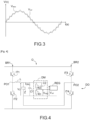
- V mes measured across the first resistor R1 is shown in figure 3 in solid lines, in the case where the measuring device is connected to the output of a voltage inverter.
- the desired reference voltage at the output of the capacitor V ref is a sinusoidal voltage shown in dotted lines.
- the voltage V mes is substantially the superposition of a sinusoidal voltage V ref and an alternating triangle voltage representing the supply current of the first capacitor.
- the measuring device has the advantage of comprising only passive components. It is simple, inexpensive and has a relatively low mass. This allows its easy integration into an inverter device, for example, to ensure the regulation of a low or high power voltage inverter.
- this DM measuring device has the advantage of being free of magnetic elements. This avoids problems related to saturation of the magnetic material, in particular the non-linearity of the measurement.
- the invention also relates to an inverter device comprising a single-phase inverter intended to transform a direct voltage into a single-phase voltage.
- FIG. 4 An example of such a DO inverter device according to the invention is shown in figure 4 .
- the inverter O comprises four controllable power switches IT1, IT2, IT3, IT4 mounted in an H-bridge.
- the H-bridge comprises two branches BR1 and BR2 each comprising two switches connected in series.
- the first branch BR1 comprises a first switch IT1 and a second switch IT2 connected in series via a first point PO1 called the first midpoint.
- the second branch BR2 comprises a third switch IT3 and a fourth switch IT4 connected in series via a second point PO2 called the second midpoint.
- the inverter O also includes an output low-pass filter formed by the first capacitor C1 and the inductor L. Voltage inverters usually include this type of low-pass filter.
- the first capacitor C1 eliminates the DC component of the voltage and the inductance L controls the level and variations of the current I LOAD flowing in the line including the inductance.
- the first midpoint PO1 is connected to a first terminal of the first capacitor C1 via the inductance L and the second midpoint PO2 is connected to a second terminal of the first capacitor C1.
- the period T AC mentioned above is the switching period of the switches.
- the period of the alternating part of the current flowing in the inductance L is equal to the switching period of the switches.
- the output voltage of inverter O is the voltage across the first capacitor C1.
- the user impedance Z is connected in parallel with the first capacitor C1.
- the inverter device DO also includes a measuring device DM as shown in figure 2 .
- the DM measuring device has the advantage of using the first capacitor C1 usually present in voltage inverters, to deliver the desired measurement.
- the measuring device DM comprises the first capacitor C1.
- the inverter device DO comprises a regulator REG configured to control the power switches IT1 to IT4 from the voltage V mes across the terminals of the first resistor R1 and a reference sinusoidal voltage V ref .
- the reference voltage V ref is, for example, the supply voltage of the desired user impedance.
- the regulator REG is advantageously configured to control the power switches IT1 to IT4 from the voltage across the terminals of the first resistor V mes and the reference sinusoidal voltage V ref so that the supply voltage of the measuring device DM or supply voltage of the user impedance Z is substantially equal to the reference voltage V ref .
- the REG regulator is advantageously configured to control switches controllable by pulse width modulation (MLI or PWM for "Pulse Width Modulation”), for example with hysteresis or any other type of PWM control.
- MMI pulse width modulation
- PWM Pulse Width Modulation
- the REG regulator is configured to deliver commands causing the switches to switch at a switching frequency Fd with a duty cycle Rc defined from the voltage V mes and the reference voltage V ref .
- the inverter device may comprise several single-phase inverters as shown in figure 4 , connected in parallel, each being associated with a measuring device according to the invention and with a control device.
- the different inverters are associated with separate measuring devices and separate control devices.
- control devices are advantageously configured to control the controllable electronic switches of the inverters so that each inverter delivers one of the phases of a three-phase alternating voltage of fixed frequency and the three inverters deliver the three phases of the three-phase voltage.
- This type of control is conventional for those skilled in the art.
- the control device is, for example, configured so that each inverter provides an alternating voltage at 400 Hz of effective voltage of 300 V, the three alternating voltages being phase-shifted so as to form the phases of a three-phase alternating voltage, from a direct voltage of 540 V.
- This configuration makes it possible to provide partial availability of the DO inverter device in the event of a failure of one of the inverters.
- the regulator may include one or more dedicated electronic circuits or a general purpose circuit.
- Each electronic circuit can comprise The REG regulator advantageously comprises analog means, such as for example at least one comparator and/or at least one amplifier and/or at least one logic gate.
- the regulator comprises a reprogrammable computing machine (e.g. a processor or microcontroller) and/or a calculator executing a program comprising a sequence of instructions and/or a dedicated computing machine (e.g. a set of logic gates such as an FPGA, a DSP or an ASIC, or any other hardware module) and/or analog components.
- a reprogrammable computing machine e.g. a processor or microcontroller
- a calculator executing a program comprising a sequence of instructions and/or a dedicated computing machine (e.g. a set of logic gates such as an FPGA, a DSP or an ASIC, or any other hardware module) and/or analog components.
- the REG regulator includes, for example, one or more attack devices (or “drivers”) to control the successive switching of each of the switches.
Landscapes
- Physics & Mathematics (AREA)
- General Physics & Mathematics (AREA)
- Engineering & Computer Science (AREA)
- Power Engineering (AREA)
- Computer Hardware Design (AREA)
- Microelectronics & Electronic Packaging (AREA)
- Inverter Devices (AREA)
- Measurement Of Current Or Voltage (AREA)
Claims (3)
- Wechselrichtervorrichtung (DO) zum Umwandeln einer Gleichspannung in eine einphasige Spannung, wobei die Wechselrichtervorrichtung (DO) einen Tiefpassfilter, eine Messvorrichtung (DM) und vier Leistungsschalter umfasst, die in einer H-Brückenschaltung angeordnet sind, wobei der Tiefpassfilter einen ersten Kondensator (C1) und eine Induktivität (L) umfasst, wobei die Messvorrichtung (DM) so konfiguriert ist, dass sie eine Spannung liefert, die einer Überlagerung einer an die Klemmen der Messvorrichtung (DM) angelegten Eingangsspannung und einer Spannung entspricht, die ein Abbild eines Stroms ist, der in dem ersten Kondensator (C1) fließt, an dessen Klemmen die Eingangsspannung angelegt ist, wobei die Messvorrichtung (DM) Folgendes umfasst:- einen parallel zum ersten Kondensator (C1) geschalteten Ableitungsfilter (FD), der einen zweiten Kondensator (C2) und einen ersten Widerstand (R1) umfasst, der in Reihe mit dem zweiten Kondensator (C2) geschaltet ist,- einen zweiten Widerstand (R2), der parallel zu dem zweiten Kondensator (C2) geschaltet ist;wobei die Brücke zwei Zweige umfasst, die jeweils zwei in Reihe geschaltete Schalter aufweisen, wobei ein erster Mittelpunkt (PO1) die beiden Schalter eines ersten der beiden Zweige verbindet und ein zweiter Mittelpunkt (PO2) die beiden Schalter eines zweiten der beiden Zweige verbindet, wobei der erste Mittelpunkt (PO1) über die Induktivität (L) mit einem ersten Anschluss des ersten Kondensators (C1) verbunden ist und der zweite Mittelpunkt (PO2) mit einem zweiten Anschluss des ersten Kondensators (C1) verbunden ist.
- Wechselrichtervorrichtung (DO) nach Anspruch 1, wobei der Ableitungsfilter (FD) eine Zeitkonstante aufweist, die kleiner als das Zehnfache einer vorbestimmten maximalen Periode des Eingangsstroms ist.
- Wechselrichtervorrichtung (DO) nach einem der Ansprüche 1 oder 2, umfassend einen Regler (REG), der so konfiguriert ist, dass er die Schalter in Abhängigkeit von der an die Anschlüsse des ersten Widerstands (R1) gelieferten Spannung steuert.
Applications Claiming Priority (1)
| Application Number | Priority Date | Filing Date | Title |
|---|---|---|---|
| FR2013299A FR3117601B1 (fr) | 2020-12-15 | 2020-12-15 | Dispositif de mesure |
Publications (2)
| Publication Number | Publication Date |
|---|---|
| EP4016091A1 EP4016091A1 (de) | 2022-06-22 |
| EP4016091B1 true EP4016091B1 (de) | 2024-08-28 |
Family
ID=74347424
Family Applications (1)
| Application Number | Title | Priority Date | Filing Date |
|---|---|---|---|
| EP21213098.3A Active EP4016091B1 (de) | 2020-12-15 | 2021-12-08 | Wechselrichtervorrichtung mit einer spannungsmessvorrichtung |
Country Status (3)
| Country | Link |
|---|---|
| US (1) | US11757372B2 (de) |
| EP (1) | EP4016091B1 (de) |
| FR (1) | FR3117601B1 (de) |
Family Cites Families (6)
| Publication number | Priority date | Publication date | Assignee | Title |
|---|---|---|---|---|
| US6341076B1 (en) * | 2000-05-23 | 2002-01-22 | Next Power Corporation | Loss reduction circuit for switching power converters |
| JP4631921B2 (ja) * | 2008-03-26 | 2011-02-16 | ソニー株式会社 | 圧電素子の駆動装置および圧電素子駆動周波数の制御方法 |
| US20120068548A1 (en) * | 2010-09-16 | 2012-03-22 | Advantest Corporation | Wireless power supply apparatus |
| US9733288B2 (en) * | 2015-10-02 | 2017-08-15 | Continental Automotive Systems, Inc. | Apparatus and method for determining a resonant frequency of an LC circuit in situ, by comparing voltage and current polarity changes |
| WO2017076366A1 (zh) * | 2015-11-06 | 2017-05-11 | 汪洪亮 | 五电平逆变器拓扑电路及三相五电平逆变器拓扑电路 |
| US10958167B2 (en) * | 2018-08-08 | 2021-03-23 | Qualcomm Incorporated | Current sensing in an on-die direct current-direct current (DC-DC) converter for measuring delivered power |
-
2020
- 2020-12-15 FR FR2013299A patent/FR3117601B1/fr active Active
-
2021
- 2021-12-08 EP EP21213098.3A patent/EP4016091B1/de active Active
- 2021-12-13 US US17/549,482 patent/US11757372B2/en active Active
Also Published As
| Publication number | Publication date |
|---|---|
| EP4016091A1 (de) | 2022-06-22 |
| FR3117601B1 (fr) | 2023-02-24 |
| FR3117601A1 (fr) | 2022-06-17 |
| US20220190740A1 (en) | 2022-06-16 |
| US11757372B2 (en) | 2023-09-12 |
Similar Documents
| Publication | Publication Date | Title |
|---|---|---|
| EP0654887B1 (de) | Unterbrechungsfreie Stromversorgung mit gemeinsamem Nullleiter und Doppelaufwärtskonverter | |
| FR2745446A1 (fr) | Circuit integre de correction de facteur de puissance | |
| EP0612982B2 (de) | Messschaltung für Widerstandssensor, insbesondere Krafstoffmesser | |
| FR2632130A1 (fr) | Systeme a fonctionnement parallele pour des convertisseurs delivrant un courant alternatif | |
| FR3040494B1 (fr) | Systeme electrique comportant un dispositif d'evaluation d'un defaut d'isolation, vehicule automobile comportant un tel systeme electrique et procede d'evaluation d'un defaut d'isolation | |
| EP0278193B1 (de) | Schaltung zum Messen des die Primärwicklung des Ausgangstransformators eines Wechselrichters durch fliessenden Gleichstromanteiles | |
| EP4016091B1 (de) | Wechselrichtervorrichtung mit einer spannungsmessvorrichtung | |
| US4591810A (en) | Pulse width modulator for electronic watthour metering | |
| EP0568471B1 (de) | Einrichtung zur Überwachung eines homopolaren Fehlers im Stromnetz | |
| FR2685474A1 (fr) | Circuit d'exploitation pour capteur inductif dont l'inductance depend de la grandeur a mesurer. | |
| FR2783370A1 (fr) | Dispositif d'alimentation a onduleur dont la puissance delivree est controlee | |
| EP0903829A1 (de) | Filteranordnung mit Steuerschaltung elektrische Vorrichtung damit | |
| FR2998736A1 (fr) | Procede de conversion de courant alternatif en courant continu et dispositif associe | |
| FR2501377A1 (fr) | Wattheuremetre electronique | |
| FR2665999A1 (fr) | Dispositif d'obtention d'une tension continue reglable. | |
| EP3840205B1 (de) | Wechselstrom-wechselstrom-wandler, der eine matrix aus bidirektionalen schaltern mit programmierbarer konfiguration umfasst | |
| WO1998025334A1 (fr) | Generateur d'arc electrique a onduleur et a alimentation triphasee | |
| US6597230B2 (en) | Electronic device | |
| EP1894289A2 (de) | Leistungswandler mit hohem wirkungsgrad und modulator und sender zu dessen anwendung | |
| JPH09508972A (ja) | 三相交流電圧検出用高速応答方法および装置 | |
| CA2869170A1 (fr) | Generateur de courant et procede de generation d'impulsions de courant | |
| EP0600809A1 (de) | Wechselstrom-dynamische Ausgleichvorrichtung | |
| EP1326327A1 (de) | Abtast-Phasendetektor | |
| EP2378651B1 (de) | Verfahren und Vorrichtung zur Steuerung der Spannung an den Klemmen einer Last, die über ein Einspeisungssystem mit Strom versorgt wird | |
| EP4572122A1 (de) | Statischer stromwandler, der konfiguriert ist, einen wert einer filterinduktivität zu messen |
Legal Events
| Date | Code | Title | Description |
|---|---|---|---|
| PUAI | Public reference made under article 153(3) epc to a published international application that has entered the european phase |
Free format text: ORIGINAL CODE: 0009012 |
|
| STAA | Information on the status of an ep patent application or granted ep patent |
Free format text: STATUS: THE APPLICATION HAS BEEN PUBLISHED |
|
| AK | Designated contracting states |
Kind code of ref document: A1 Designated state(s): AL AT BE BG CH CY CZ DE DK EE ES FI FR GB GR HR HU IE IS IT LI LT LU LV MC MK MT NL NO PL PT RO RS SE SI SK SM TR |
|
| STAA | Information on the status of an ep patent application or granted ep patent |
Free format text: STATUS: REQUEST FOR EXAMINATION WAS MADE |
|
| 17P | Request for examination filed |
Effective date: 20221020 |
|
| RBV | Designated contracting states (corrected) |
Designated state(s): AL AT BE BG CH CY CZ DE DK EE ES FI FR GB GR HR HU IE IS IT LI LT LU LV MC MK MT NL NO PL PT RO RS SE SI SK SM TR |
|
| GRAP | Despatch of communication of intention to grant a patent |
Free format text: ORIGINAL CODE: EPIDOSNIGR1 |
|
| STAA | Information on the status of an ep patent application or granted ep patent |
Free format text: STATUS: GRANT OF PATENT IS INTENDED |
|
| INTG | Intention to grant announced |
Effective date: 20240417 |
|
| GRAJ | Information related to disapproval of communication of intention to grant by the applicant or resumption of examination proceedings by the epo deleted |
Free format text: ORIGINAL CODE: EPIDOSDIGR1 |
|
| STAA | Information on the status of an ep patent application or granted ep patent |
Free format text: STATUS: REQUEST FOR EXAMINATION WAS MADE |
|
| GRAP | Despatch of communication of intention to grant a patent |
Free format text: ORIGINAL CODE: EPIDOSNIGR1 |
|
| STAA | Information on the status of an ep patent application or granted ep patent |
Free format text: STATUS: GRANT OF PATENT IS INTENDED |
|
| GRAS | Grant fee paid |
Free format text: ORIGINAL CODE: EPIDOSNIGR3 |
|
| GRAA | (expected) grant |
Free format text: ORIGINAL CODE: 0009210 |
|
| STAA | Information on the status of an ep patent application or granted ep patent |
Free format text: STATUS: THE PATENT HAS BEEN GRANTED |
|
| INTC | Intention to grant announced (deleted) | ||
| INTG | Intention to grant announced |
Effective date: 20240716 |
|
| RAP1 | Party data changed (applicant data changed or rights of an application transferred) |
Owner name: SAFRAN ELECTRICAL & POWER |
|
| AK | Designated contracting states |
Kind code of ref document: B1 Designated state(s): AL AT BE BG CH CY CZ DE DK EE ES FI FR GB GR HR HU IE IS IT LI LT LU LV MC MK MT NL NO PL PT RO RS SE SI SK SM TR |
|
| REG | Reference to a national code |
Ref country code: CH Ref legal event code: EP |
|
| REG | Reference to a national code |
Ref country code: DE Ref legal event code: R096 Ref document number: 602021017869 Country of ref document: DE |
|
| REG | Reference to a national code |
Ref country code: IE Ref legal event code: FG4D Free format text: LANGUAGE OF EP DOCUMENT: FRENCH |
|
| REG | Reference to a national code |
Ref country code: LT Ref legal event code: MG9D |
|
| PGFP | Annual fee paid to national office [announced via postgrant information from national office to epo] |
Ref country code: DE Payment date: 20241121 Year of fee payment: 4 |
|
| PG25 | Lapsed in a contracting state [announced via postgrant information from national office to epo] |
Ref country code: NO Free format text: LAPSE BECAUSE OF FAILURE TO SUBMIT A TRANSLATION OF THE DESCRIPTION OR TO PAY THE FEE WITHIN THE PRESCRIBED TIME-LIMIT Effective date: 20241128 |
|
| REG | Reference to a national code |
Ref country code: AT Ref legal event code: MK05 Ref document number: 1718513 Country of ref document: AT Kind code of ref document: T Effective date: 20240828 |
|
| PG25 | Lapsed in a contracting state [announced via postgrant information from national office to epo] |
Ref country code: NL Free format text: LAPSE BECAUSE OF FAILURE TO SUBMIT A TRANSLATION OF THE DESCRIPTION OR TO PAY THE FEE WITHIN THE PRESCRIBED TIME-LIMIT Effective date: 20240828 Ref country code: PT Free format text: LAPSE BECAUSE OF FAILURE TO SUBMIT A TRANSLATION OF THE DESCRIPTION OR TO PAY THE FEE WITHIN THE PRESCRIBED TIME-LIMIT Effective date: 20241230 Ref country code: GR Free format text: LAPSE BECAUSE OF FAILURE TO SUBMIT A TRANSLATION OF THE DESCRIPTION OR TO PAY THE FEE WITHIN THE PRESCRIBED TIME-LIMIT Effective date: 20241129 Ref country code: PL Free format text: LAPSE BECAUSE OF FAILURE TO SUBMIT A TRANSLATION OF THE DESCRIPTION OR TO PAY THE FEE WITHIN THE PRESCRIBED TIME-LIMIT Effective date: 20240828 Ref country code: FI Free format text: LAPSE BECAUSE OF FAILURE TO SUBMIT A TRANSLATION OF THE DESCRIPTION OR TO PAY THE FEE WITHIN THE PRESCRIBED TIME-LIMIT Effective date: 20240828 |
|
| PG25 | Lapsed in a contracting state [announced via postgrant information from national office to epo] |
Ref country code: BG Free format text: LAPSE BECAUSE OF FAILURE TO SUBMIT A TRANSLATION OF THE DESCRIPTION OR TO PAY THE FEE WITHIN THE PRESCRIBED TIME-LIMIT Effective date: 20240828 |
|
| PG25 | Lapsed in a contracting state [announced via postgrant information from national office to epo] |
Ref country code: LV Free format text: LAPSE BECAUSE OF FAILURE TO SUBMIT A TRANSLATION OF THE DESCRIPTION OR TO PAY THE FEE WITHIN THE PRESCRIBED TIME-LIMIT Effective date: 20240828 |
|
| REG | Reference to a national code |
Ref country code: NL Ref legal event code: MP Effective date: 20240828 |
|
| PG25 | Lapsed in a contracting state [announced via postgrant information from national office to epo] |
Ref country code: IS Free format text: LAPSE BECAUSE OF FAILURE TO SUBMIT A TRANSLATION OF THE DESCRIPTION OR TO PAY THE FEE WITHIN THE PRESCRIBED TIME-LIMIT Effective date: 20241228 Ref country code: AT Free format text: LAPSE BECAUSE OF FAILURE TO SUBMIT A TRANSLATION OF THE DESCRIPTION OR TO PAY THE FEE WITHIN THE PRESCRIBED TIME-LIMIT Effective date: 20240828 |
|
| PG25 | Lapsed in a contracting state [announced via postgrant information from national office to epo] |
Ref country code: HR Free format text: LAPSE BECAUSE OF FAILURE TO SUBMIT A TRANSLATION OF THE DESCRIPTION OR TO PAY THE FEE WITHIN THE PRESCRIBED TIME-LIMIT Effective date: 20240828 |
|
| PG25 | Lapsed in a contracting state [announced via postgrant information from national office to epo] |
Ref country code: ES Free format text: LAPSE BECAUSE OF FAILURE TO SUBMIT A TRANSLATION OF THE DESCRIPTION OR TO PAY THE FEE WITHIN THE PRESCRIBED TIME-LIMIT Effective date: 20240828 Ref country code: RS Free format text: LAPSE BECAUSE OF FAILURE TO SUBMIT A TRANSLATION OF THE DESCRIPTION OR TO PAY THE FEE WITHIN THE PRESCRIBED TIME-LIMIT Effective date: 20241128 |
|
| PG25 | Lapsed in a contracting state [announced via postgrant information from national office to epo] |
Ref country code: RS Free format text: LAPSE BECAUSE OF FAILURE TO SUBMIT A TRANSLATION OF THE DESCRIPTION OR TO PAY THE FEE WITHIN THE PRESCRIBED TIME-LIMIT Effective date: 20241128 Ref country code: PT Free format text: LAPSE BECAUSE OF FAILURE TO SUBMIT A TRANSLATION OF THE DESCRIPTION OR TO PAY THE FEE WITHIN THE PRESCRIBED TIME-LIMIT Effective date: 20241230 Ref country code: PL Free format text: LAPSE BECAUSE OF FAILURE TO SUBMIT A TRANSLATION OF THE DESCRIPTION OR TO PAY THE FEE WITHIN THE PRESCRIBED TIME-LIMIT Effective date: 20240828 Ref country code: NO Free format text: LAPSE BECAUSE OF FAILURE TO SUBMIT A TRANSLATION OF THE DESCRIPTION OR TO PAY THE FEE WITHIN THE PRESCRIBED TIME-LIMIT Effective date: 20241128 Ref country code: NL Free format text: LAPSE BECAUSE OF FAILURE TO SUBMIT A TRANSLATION OF THE DESCRIPTION OR TO PAY THE FEE WITHIN THE PRESCRIBED TIME-LIMIT Effective date: 20240828 Ref country code: LV Free format text: LAPSE BECAUSE OF FAILURE TO SUBMIT A TRANSLATION OF THE DESCRIPTION OR TO PAY THE FEE WITHIN THE PRESCRIBED TIME-LIMIT Effective date: 20240828 Ref country code: IS Free format text: LAPSE BECAUSE OF FAILURE TO SUBMIT A TRANSLATION OF THE DESCRIPTION OR TO PAY THE FEE WITHIN THE PRESCRIBED TIME-LIMIT Effective date: 20241228 Ref country code: HR Free format text: LAPSE BECAUSE OF FAILURE TO SUBMIT A TRANSLATION OF THE DESCRIPTION OR TO PAY THE FEE WITHIN THE PRESCRIBED TIME-LIMIT Effective date: 20240828 Ref country code: GR Free format text: LAPSE BECAUSE OF FAILURE TO SUBMIT A TRANSLATION OF THE DESCRIPTION OR TO PAY THE FEE WITHIN THE PRESCRIBED TIME-LIMIT Effective date: 20241129 Ref country code: FI Free format text: LAPSE BECAUSE OF FAILURE TO SUBMIT A TRANSLATION OF THE DESCRIPTION OR TO PAY THE FEE WITHIN THE PRESCRIBED TIME-LIMIT Effective date: 20240828 Ref country code: ES Free format text: LAPSE BECAUSE OF FAILURE TO SUBMIT A TRANSLATION OF THE DESCRIPTION OR TO PAY THE FEE WITHIN THE PRESCRIBED TIME-LIMIT Effective date: 20240828 Ref country code: BG Free format text: LAPSE BECAUSE OF FAILURE TO SUBMIT A TRANSLATION OF THE DESCRIPTION OR TO PAY THE FEE WITHIN THE PRESCRIBED TIME-LIMIT Effective date: 20240828 Ref country code: AT Free format text: LAPSE BECAUSE OF FAILURE TO SUBMIT A TRANSLATION OF THE DESCRIPTION OR TO PAY THE FEE WITHIN THE PRESCRIBED TIME-LIMIT Effective date: 20240828 |
|
| PG25 | Lapsed in a contracting state [announced via postgrant information from national office to epo] |
Ref country code: RO Free format text: LAPSE BECAUSE OF FAILURE TO SUBMIT A TRANSLATION OF THE DESCRIPTION OR TO PAY THE FEE WITHIN THE PRESCRIBED TIME-LIMIT Effective date: 20240828 Ref country code: SM Free format text: LAPSE BECAUSE OF FAILURE TO SUBMIT A TRANSLATION OF THE DESCRIPTION OR TO PAY THE FEE WITHIN THE PRESCRIBED TIME-LIMIT Effective date: 20240828 Ref country code: DK Free format text: LAPSE BECAUSE OF FAILURE TO SUBMIT A TRANSLATION OF THE DESCRIPTION OR TO PAY THE FEE WITHIN THE PRESCRIBED TIME-LIMIT Effective date: 20240828 |
|
| PG25 | Lapsed in a contracting state [announced via postgrant information from national office to epo] |
Ref country code: EE Free format text: LAPSE BECAUSE OF FAILURE TO SUBMIT A TRANSLATION OF THE DESCRIPTION OR TO PAY THE FEE WITHIN THE PRESCRIBED TIME-LIMIT Effective date: 20240828 |
|
| PG25 | Lapsed in a contracting state [announced via postgrant information from national office to epo] |
Ref country code: CZ Free format text: LAPSE BECAUSE OF FAILURE TO SUBMIT A TRANSLATION OF THE DESCRIPTION OR TO PAY THE FEE WITHIN THE PRESCRIBED TIME-LIMIT Effective date: 20240828 |
|
| PG25 | Lapsed in a contracting state [announced via postgrant information from national office to epo] |
Ref country code: SK Free format text: LAPSE BECAUSE OF FAILURE TO SUBMIT A TRANSLATION OF THE DESCRIPTION OR TO PAY THE FEE WITHIN THE PRESCRIBED TIME-LIMIT Effective date: 20240828 Ref country code: IT Free format text: LAPSE BECAUSE OF FAILURE TO SUBMIT A TRANSLATION OF THE DESCRIPTION OR TO PAY THE FEE WITHIN THE PRESCRIBED TIME-LIMIT Effective date: 20240828 |
|
| REG | Reference to a national code |
Ref country code: DE Ref legal event code: R097 Ref document number: 602021017869 Country of ref document: DE |
|
| PLBE | No opposition filed within time limit |
Free format text: ORIGINAL CODE: 0009261 |
|
| STAA | Information on the status of an ep patent application or granted ep patent |
Free format text: STATUS: NO OPPOSITION FILED WITHIN TIME LIMIT |
|
| PG25 | Lapsed in a contracting state [announced via postgrant information from national office to epo] |
Ref country code: MC Free format text: LAPSE BECAUSE OF FAILURE TO SUBMIT A TRANSLATION OF THE DESCRIPTION OR TO PAY THE FEE WITHIN THE PRESCRIBED TIME-LIMIT Effective date: 20240828 |
|
| REG | Reference to a national code |
Ref country code: CH Ref legal event code: PL |
|
| 26N | No opposition filed |
Effective date: 20250530 |
|
| PG25 | Lapsed in a contracting state [announced via postgrant information from national office to epo] |
Ref country code: LU Free format text: LAPSE BECAUSE OF NON-PAYMENT OF DUE FEES Effective date: 20241208 |
|
| PG25 | Lapsed in a contracting state [announced via postgrant information from national office to epo] |
Ref country code: SE Free format text: LAPSE BECAUSE OF FAILURE TO SUBMIT A TRANSLATION OF THE DESCRIPTION OR TO PAY THE FEE WITHIN THE PRESCRIBED TIME-LIMIT Effective date: 20240828 |
|
| REG | Reference to a national code |
Ref country code: BE Ref legal event code: MM Effective date: 20241231 |
|
| PG25 | Lapsed in a contracting state [announced via postgrant information from national office to epo] |
Ref country code: BE Free format text: LAPSE BECAUSE OF NON-PAYMENT OF DUE FEES Effective date: 20241231 |
|
| PG25 | Lapsed in a contracting state [announced via postgrant information from national office to epo] |
Ref country code: CH Free format text: LAPSE BECAUSE OF NON-PAYMENT OF DUE FEES Effective date: 20241231 |
|
| PG25 | Lapsed in a contracting state [announced via postgrant information from national office to epo] |
Ref country code: IE Free format text: LAPSE BECAUSE OF NON-PAYMENT OF DUE FEES Effective date: 20241208 |
|
| PGFP | Annual fee paid to national office [announced via postgrant information from national office to epo] |
Ref country code: GB Payment date: 20251229 Year of fee payment: 5 |
|
| PGFP | Annual fee paid to national office [announced via postgrant information from national office to epo] |
Ref country code: FR Payment date: 20251222 Year of fee payment: 5 |