EP4014290B1 - Abstimmbarer vcsel mit kombinierter verstärkung und dbr-spiegel - Google Patents
Abstimmbarer vcsel mit kombinierter verstärkung und dbr-spiegel Download PDFInfo
- Publication number
- EP4014290B1 EP4014290B1 EP20765122.5A EP20765122A EP4014290B1 EP 4014290 B1 EP4014290 B1 EP 4014290B1 EP 20765122 A EP20765122 A EP 20765122A EP 4014290 B1 EP4014290 B1 EP 4014290B1
- Authority
- EP
- European Patent Office
- Prior art keywords
- laser
- quantum wells
- mirror
- dbr
- vcsel
- Prior art date
- Legal status (The legal status is an assumption and is not a legal conclusion. Google has not performed a legal analysis and makes no representation as to the accuracy of the status listed.)
- Active
Links
Images





Classifications
-
- H—ELECTRICITY
- H01—ELECTRIC ELEMENTS
- H01S—DEVICES USING THE PROCESS OF LIGHT AMPLIFICATION BY STIMULATED EMISSION OF RADIATION [LASER] TO AMPLIFY OR GENERATE LIGHT; DEVICES USING STIMULATED EMISSION OF ELECTROMAGNETIC RADIATION IN WAVE RANGES OTHER THAN OPTICAL
- H01S5/00—Semiconductor lasers
- H01S5/10—Construction or shape of the optical resonator, e.g. extended or external cavity, coupled cavities, bent-guide, varying width, thickness or composition of the active region
- H01S5/18—Surface-emitting [SE] lasers, e.g. having both horizontal and vertical cavities
- H01S5/183—Surface-emitting [SE] lasers, e.g. having both horizontal and vertical cavities having only vertical cavities, e.g. vertical cavity surface-emitting lasers [VCSEL]
- H01S5/18361—Structure of the reflectors, e.g. hybrid mirrors
- H01S5/18363—Structure of the reflectors, e.g. hybrid mirrors comprising air layers
- H01S5/18366—Membrane DBR, i.e. a movable DBR on top of the VCSEL
-
- H—ELECTRICITY
- H01—ELECTRIC ELEMENTS
- H01S—DEVICES USING THE PROCESS OF LIGHT AMPLIFICATION BY STIMULATED EMISSION OF RADIATION [LASER] TO AMPLIFY OR GENERATE LIGHT; DEVICES USING STIMULATED EMISSION OF ELECTROMAGNETIC RADIATION IN WAVE RANGES OTHER THAN OPTICAL
- H01S5/00—Semiconductor lasers
- H01S5/04—Processes or apparatus for excitation, e.g. pumping, e.g. by electron beams
- H01S5/041—Optical pumping
-
- H—ELECTRICITY
- H01—ELECTRIC ELEMENTS
- H01S—DEVICES USING THE PROCESS OF LIGHT AMPLIFICATION BY STIMULATED EMISSION OF RADIATION [LASER] TO AMPLIFY OR GENERATE LIGHT; DEVICES USING STIMULATED EMISSION OF ELECTROMAGNETIC RADIATION IN WAVE RANGES OTHER THAN OPTICAL
- H01S5/00—Semiconductor lasers
- H01S5/10—Construction or shape of the optical resonator, e.g. extended or external cavity, coupled cavities, bent-guide, varying width, thickness or composition of the active region
- H01S5/18—Surface-emitting [SE] lasers, e.g. having both horizontal and vertical cavities
- H01S5/183—Surface-emitting [SE] lasers, e.g. having both horizontal and vertical cavities having only vertical cavities, e.g. vertical cavity surface-emitting lasers [VCSEL]
- H01S5/18361—Structure of the reflectors, e.g. hybrid mirrors
- H01S5/18369—Structure of the reflectors, e.g. hybrid mirrors based on dielectric materials
-
- H—ELECTRICITY
- H01—ELECTRIC ELEMENTS
- H01S—DEVICES USING THE PROCESS OF LIGHT AMPLIFICATION BY STIMULATED EMISSION OF RADIATION [LASER] TO AMPLIFY OR GENERATE LIGHT; DEVICES USING STIMULATED EMISSION OF ELECTROMAGNETIC RADIATION IN WAVE RANGES OTHER THAN OPTICAL
- H01S5/00—Semiconductor lasers
- H01S5/10—Construction or shape of the optical resonator, e.g. extended or external cavity, coupled cavities, bent-guide, varying width, thickness or composition of the active region
- H01S5/18—Surface-emitting [SE] lasers, e.g. having both horizontal and vertical cavities
- H01S5/183—Surface-emitting [SE] lasers, e.g. having both horizontal and vertical cavities having only vertical cavities, e.g. vertical cavity surface-emitting lasers [VCSEL]
- H01S5/18383—Surface-emitting [SE] lasers, e.g. having both horizontal and vertical cavities having only vertical cavities, e.g. vertical cavity surface-emitting lasers [VCSEL] with periodic active regions at nodes or maxima of light intensity
-
- H—ELECTRICITY
- H01—ELECTRIC ELEMENTS
- H01S—DEVICES USING THE PROCESS OF LIGHT AMPLIFICATION BY STIMULATED EMISSION OF RADIATION [LASER] TO AMPLIFY OR GENERATE LIGHT; DEVICES USING STIMULATED EMISSION OF ELECTROMAGNETIC RADIATION IN WAVE RANGES OTHER THAN OPTICAL
- H01S5/00—Semiconductor lasers
- H01S5/30—Structure or shape of the active region; Materials used for the active region
- H01S5/34—Structure or shape of the active region; Materials used for the active region comprising quantum well or superlattice structures, e.g. single quantum well [SQW] lasers, multiple quantum well [MQW] lasers or graded index separate confinement heterostructure [GRINSCH] lasers
- H01S5/343—Structure or shape of the active region; Materials used for the active region comprising quantum well or superlattice structures, e.g. single quantum well [SQW] lasers, multiple quantum well [MQW] lasers or graded index separate confinement heterostructure [GRINSCH] lasers in AIIIBV compounds, e.g. AlGaAs-laser, InP-based laser
- H01S5/34306—Structure or shape of the active region; Materials used for the active region comprising quantum well or superlattice structures, e.g. single quantum well [SQW] lasers, multiple quantum well [MQW] lasers or graded index separate confinement heterostructure [GRINSCH] lasers in AIIIBV compounds, e.g. AlGaAs-laser, InP-based laser emitting light at a wavelength longer than 1000nm, e.g. InP based 1300 and 1500nm lasers
Definitions
- OCT optical coherence tomography
- the GaAs/AlAs material system natively has fairly high index contrast allowing epitaxially-grown mirrors supporting tuning ranges on the order of 100 nm.
- the free-spectral range (FSR) of a VCSEL cavity in optical frequency is c/(2L), where c is the speed of light and L is the total length of the laser cavity including the group delay of the mirrors (see D. I. Babic and S. W. Corzine, "Analytic expressions for the reflection delay, penetration depth, and absorptance of quarter-wave dielectric mirrors," IEEE Journal of Quantum Electronics, 28, 514-524, (1992 )), the length of the air gap and the length of the gain section and other layers.
- the laser tuning range is limited by the FSR because another lasing mode can pop up one FSR away as the device is tuned.
- the spectral gain bandwidth of the active quantum wells also has to be wide enough to allow wide tuning.
- a MEMS tunable VCSEL has one mirror on a flexible membrane coupled to a 1 ⁇ 2-VCSEL structure that combines an optical gain medium with a second, stationary reflector. See Flanders, D. C., Kuznetsov, M. E., Atia, W. A., and Johnson, B. C., "OCT system with bonded MEMS tunable mirror VCSEL swept source.” US Patent application 2016/0329682 A1 (10 November 2016 ) and Jayaraman, V., Jiang, J., Potsaid, B., Robertson, M., Heim, P. J. S., Burgner, C., John, D., Cole, G. D.,Grulkowski, I., Fujimoto, J. G., Davis, A.
- Present invention concerns a way of shortening the overall cavity length by combining the gain section with a distributed Bragg reflector (DBR).
- DBR distributed Bragg reflector
- the overall cavity length can be contracted by placing gain structures inside the DBR. This generally applies to a number of semiconductor material systems and wavelength bands, but this scheme is very well suited to the AlGaAs/GaAs material system with strained InGaAs quantum wells as a gain medium, for example.
- the invention features a vertical surface emitting laser, comprising a distributed Bragg reflector and quantum wells located in the distributed Bragg reflector.
- the quantum wells are located in shallow layers of the distributed Bragg reflector.
- the laser can be fabricated in AlGaAs/GaAs, although other material systems can be used. Also, the quantum wells might be optically pumped or electrically pumped.
- the quantum wells are located between high index layers and low index layers of the distributed Bragg reflector.
- the quantum wells are located in high index layers of the distributed Bragg reflector.
- the quantum wells are placed at antinodes of standing wave patterns in the laser.
- the high index layers of the distributed Bragg reflector can be thinner than the low index layers.
- the invention features a vertical surface emitting laser system, comprising a vertical surface emitting laser, including a distributed Bragg reflector and quantum wells located in the distributed Bragg reflector and a pump laser for optically pumping the quantum wells.
- the term “and/or” includes any and all combinations of one or more of the associated listed items. Further, the singular forms and the articles “a”, “an” and “the” are intended to include the plural forms as well, unless expressly stated otherwise. It will be further understood that the terms: includes, comprises, including and/or comprising, when used in this specification, specify the presence of stated features, integers, steps, operations, elements, and/or components, but do not preclude the presence or addition of one or more other features, integers, steps, operations, elements, components, and/or groups thereof. Further, it will be understood that when an element, including component or subsystem, is referred to and/or shown as being connected or coupled to another element, it can be directly connected or coupled to the other element or intervening elements may be present.
- Fig. 1A shows a conventional arrangement for the DBR mirror and the quantum wells in a MEMS tunable VCSEL 10.
- the MEMS tunable VCSEL 10 includes a front MEMS membrane structure 214 that carries a membrane mirror 250.
- a 1 ⁇ 2 or half VCSEL chip or device 112 is separated from the front MEMS membrane structure 214 by an adjustable air optical gap 105, the length of which along the optical axis is tuned by deflecting the membrane structure.
- the gain medium GM is separate from the DBR mirror in the half VCSEL device 112.
- the overall cavity length is contracted in the direction of the optical axis by placing the gain medium GM inside the DBR stack mirror to create a combined gain medium and DBR mirror GM/DBR.
- the quantum well layers QW1-QW4. are preferably placed high in the stack of the DBR mirror where the electrical fields of the reflected light are strongest. This maximizes their respective contributions to the gain.
- This combined gain medium and DBR mirror, the GM/DBR is generally applicable to a number of semiconductor material systems and wavelength bands.
- Common material systems are based on III-V semiconductor materials, including binary materials, such as GaN, GaAs, InP, GaSb, InAs, as well as tertiary, quaternary, and pentenary alloys, such as InGaN, InAlGaN, InGaP, AlGaAs, InGaAs, GaInNAs, GaInNAsSb, AlInGaAs, InGaAsP, AlGaAsSb, AlGaInAsSb, AlAsSb, InGaSb, InAsSb, and InGaAsSb.
- binary materials such as GaN, GaAs, InP, GaSb, InAs, as well as tertiary, quaternary, and pentenary alloys, such as InGaN, InAlGaN, InGaP
- these material systems support operating wavelengths from about 400 nanometers (nm) to 2000 nm, including longer wavelength ranges extending into multiple micrometer wavelengths.
- Semiconductor quantum well and quantum dot gain regions are typically used to obtain especially wide gain and spectral emission bandwidths.
- Quantum well layers may be purposely strained or unstrained depending on the exact materials and the desired wavelength coverage.
- the combined gain medium and DBR mirror, the GM/DBR is very well suited to the AlGaAs/GaAs material system with strained InGaAs quantum wells as a gain medium.
- This system lases in a band around 1050 nm.
- the high index layers H are GaAs
- the low index layers L are AlAs or similar high A1 content AlGaAs alloys.
- the combined gain medium and DBR mirror, the GM/DBR, is optically pumped in a current embodiment.
- the laser emission light and pump light needs to come through the MEMS membrane structure if the substrate is absorptive at the pump wavelength, as it is for a GaAs substrate.
- the VCSEL emission may be configured to come out of the MEMS side, the substrate side, or both.
- the MEMS mirror 250 is often curved for spatial mode control; but, it does not necessarily have to be so, for example in cases where thermal lensing in the half VCSEL device 112 is strong.
- gain quantum wells For optically pumped lasers, gain quantum wells have to be placed inside the pump-absorbing low-bandgap Bragg reflector layers.
- the concept of placing gain section inside the Bragg reflector mirror can also be applied to the electrically pumped semiconductor lasers.
- Figs. 2A , 2B , and 2C are plots of energy of the GaAs valence and conduction bands in electron volts (eV), wavelength in nanometers (nm) as a function of optical gap in micrometers and gain per well as a function of optical gap in micrometers for a conventional tunable VCSEL.
- the graphs show about 90 nm of tuning range for the VCSEL by changing the optical gap by about 0.5 pm for a six well VCSEL of conventional design.
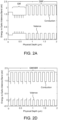
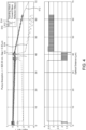
- Figs. 2D , 2E , and 2F are plots of energy of the GaAs valence and conduction bands in electron volts (eV), wavelength in nanometers (nm) as a function of optical gap in micrometers and gain per well as a function of optical gap 105 in micrometers for a tunable VCSEL employing the combined gain medium and DBR mirror GM/DBR.
- the graphs show about 110 nm of tuning range for the VCSEL by changing the optical gap 105 by less than 0.5 pm. This improved performance is due to the much shorter cavity length afforded by the combined gain medium and DBR mirror GM/DBR.
- Figs. 2C and 2F show the conduction and valence band edges for the example where the materials are GaAs/Al x Ga l-x As/In y Ga l-y As.
- Fig. 3 shows standing wave patterns (magnitude of the electric field plotted) inside the gain embedded DBR VCSEL 100 with six quantum wells QW1-QW6.
- the electric field is shown at the band center 1040 nm, short band edge 994 nm, and long band edge 1090 nm.
- the refractive index profile of the semiconductor and dielectric materials show the structure of the DBR and placement of the quantum wells.
- the wells QW1-QW6 are placed, and roughly aligned with the antinodes in the DBR of the standing wave patterns for all wavelengths.
- Another advantage of the combined gain medium and DBR mirror GM/DBR is that if more gain is required, more quantum wells can be added without appreciably changing the tuning range.
- pump absorption is weak enough that wells further away from the pump laser are still pumped appreciably.
- Fig. 4 shows standing wave patterns (magnitude of the electric field plotted) inside the gain embedded DBR VCSEL 100 for the pump light at 825 nm. As shown, there is enough pump light to power deeper wells.
- This gain embedded DBR structure is compatible with optical pumping. Absorption into the first few GaAs layers of the DBR channel electron-hole pairs into the co-located strained quantum well layers. The reflected waves are small, and the overall absorption constant is about half that of bulk GaAs since half of the material in the DBR is non-absorbing AlGaAs.
- the propagating optical power density is calculated from the Poynting vector, and is proportional to n
- the incident forward wave in air from the left is normalized to a value of n
- 2 1.
- the light absorbed in the gain region is about 12% in this example.
- the forward and backward waves are plotted, along with the standing wave.
- the power would be high enough to use the VCSEL light directly, without requiring a separate amplification stage, e.g., semiconductor optical amplifier (SOA).
- SOA semiconductor optical amplifier
- the quantum wells QW need to be placed in a region of high optical field, preferably at an antinode of the VCSEL's standing wave pattern.
- the strained InGaAs quantum well is placed near the junction of the GaAs and Al 0.97 Ga 0.03 As, which is where the antinode is, as shown in Fig. 3 .
- the GaAs also serves as an absorbing region where pump light is absorbed, and the excited electrons and holes are funneled into the potential well formed by the strained InGaAs quantum wells.
- the GaAs and Al 0.97 Ga 0.03 As regions have equal optical lengths to maximize the reflectivity of the DBR.
- thicker GaAs could be grown with thinner Al 0.97 Ga 0.03 As in order to keep the DBR period the same. This would have the effect of increasing optical absorption while decreasing the DBR reflectivity and bandwidth. This might be a favorable tradeoff in some cases.
- Hybrid structures can be employed that are intermediate between a separate gain region structure and a gain embedded DBR structure.
- One way this can be done is by increasing the GaAs thickness near the quantum wells and decreasing the AlGaAs thickness to keep the same DBR period.
- Fig. 5A shows a structure of this type, showing the energy in the valence and conduction bands in electron Voltage (eV) in the combined gain medium and DBR mirror GM/DBR
- eV electron Voltage
- the quantum wells QW1-QW6 are located within respective high refractive index layers H, and the low refractive index layers have a reduced thickness.
- the optical period corresponds to roughly half a wavelength.
- Figs. 5B and 5C are plots of wavelength nanometers and gain per well as a function of the optical air gap. Calculations for three of these structures are shown where the GaAs/AlGaAs DBR period optical thicknesses are 50/50, 63/37, and 75/25 in percent thickness. Adding GaAs is advantageous since it funnels more pump light into excitation of the quantum wells.
- a 100/0 thickness variant would be considered a well "outside" the DBR.
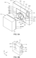
- FIGs. 6A and 6B A specific design for a MEMS tunable VCSEL 100 is presented in Figs. 6A and 6B that employs the combined gain medium and DBR mirror, the GM/DBR. While many designs are possible, this one is formed by bonding the half VCSEL chip or device 1 12 to a silicon MEMS optical membrane device 110, which has an electrostatically movable mirror for wavelength tuning.
- the optical membrane device 110 comprises handle wafer material 210 that functions as a support.
- the handle is made from doped silicon, with a resistivity ⁇ 0.1 ohm-cm, carrier concentration >1 ⁇ 10 17 cm -3 , to facilitate electrical contact.
- An optical membrane or device layer 212 is added to the handle wafer material 210.
- silicon on insulator (SOI) wafers are used.
- An optical membrane structure 214 is formed in this optical membrane layer 212.
- the membrane layer 212 is silicon that is low doped with resistivity >1 ohm-cm, carrier concentration ⁇ 5 ⁇ 10 15 cm -3 , to minimize free carrier absorption of the transmitted light.
- the membrane layer surface is usually additionally doped by ion implantation to create a highly doped surface layer (doped usually to > 1 ⁇ 10 18 cm -3 , but at least 1 ⁇ 10 17 cm -3 and at least 200 Angstroms (A) thick, usually 500-2000 A thick). This method minimizes optical absorption in the membrane layer itself that would occur if the entire layer were highly doped.
- An insulating (buried silicon dioxide) layer 216 separates the optical membrane layer 212 from the handle wafer material 210.
- the insulating layer 216 functions as a sacrificial/release layer, which is partially removed to release the membrane structure 214 from the handle wafer material 210. Then during operation, the remaining portions of the insulating layer 216 provide electrical isolation between the patterned device layer 212 and the handle material 210.
- the membrane structure 214 comprises a body portion 218.
- the optical axis of the device 100 passes concentrically through this body portion 218 and orthogonal to a plane defined by the membrane layer 212.
- a diameter of this body portion 218 is preferably 300 to 600 micrometers; currently it is about 500 micrometers.
- Tethers 220 (four tethers in the illustrated example) are defined and delineated by arcuate slots 225 fabricated into the device layer 212.
- the tethers 220 extend radially from the body portion 218 to an outer portion 222, which comprises the ring where the tethers 220 terminate.
- a spiral tether pattern is used.
- a membrane mirror dot 250 is disposed on body portion 218 of the membrane structure 214.
- the membrane mirror 250 is optically curved to form an optically concave optical element to thereby form a curved mirror laser cavity.
- the membrane mirror 250 is a flat mirror, or even possibly convex.
- this curvature can be created by forming a depression in the body portion 218 and then depositing the material layer or layers that form mirror 250 over that depression.
- the membrane mirror 250 can be deposited with a high amount of compressive material stress that will result in its curvature.
- the membrane mirror dot 250 is preferably a reflecting dielectric mirror stack. In some examples, it is a dichroic mirror-filter that provides a defined reflectivity, such as between 1 and 99.9%, to the wavelengths of laser light generated in the laser 100, whereas the optical dot 250 is transmissive to wavelengths of light that are used to optically pump the active region in the VCSEL device 112. In still other examples, the optical dot is a reflective metal layer such as aluminum or gold.
- Electrode wire bond pad 334A is used to provide an electrical connection to the membrane layer 212 and thus the membrane structure 214.
- the handle wire bond pad 334B is used to provide an electrical connection to the handle wafer material 210.
- the half VCSEL device 112 generally comprises an antireflective coating 114, which is optional, and the combined gain medium and DBR mirror GM/DBR.
- the cap layer can be used between the antireflective coating 114, if present, and the combined gain medium and DBR mirror GM/DBR.
- the cap layer protects the active region from the surface/interface effects at the interface to the AR coating and/or air.
- the combined gain medium and DBR mirror GM/DBR is a dichroic mirror-filter that provides a defined reflectivity, such as greater than 99% to the wavelengths of laser light generated in the laser 100, whereas the GM/DBR is transmissive to wavelengths of light that are used to optically pump the active region in the VCSEL device 112, thus allowing the half VCSEL device 112 to function as an input port of pump light.
- the mirror reflectivities tend toward higher numbers for light around 1050 nm in wavelength.
- the reflectivity of the GM/DBR is about 99.99%.
- the front mirror dot 250 is usually 99% or greater. In current embodiments, the mirror dot 250 has a reflectivity of about 99.4% or higher.
- the VCSEL device is electrically or optically pumped.
- the generated light resonates between the combined gain medium and DBR mirror GM/DBR and membrane mirror 250.
- the wavelength of the generated light is tuned within the scan band of the device by the out of plane electrostatic deflection of the body portion 218 and thus the membrane mirror 250 by controlling the electrostatic field between the body portion 218 and the handle wafer material 210 and/or the half VCSEL device 112.
- Fig. 6B is schematic view showing the hidden bond pads VP1-VP4 on the half VCSEL device 112.
- the thin gold pads VP1-VP4 on the 1 ⁇ 2 VCSEL device 112 are thermocompression bonded to corresponding membrane pads MP1, MP2, MP3, and MP4 of the MEMS membrane (mirror) device 110 by placing them in contact at high pressure and temperature to form the bond. Typically, this is done at 300 - 360°C and 1 - 10N force.
- elevated temperature bonding methods such as gold-tin and/or eutectic soldering, can be used to produce a similar effect, however.
- the bond pad arrangement is asymmetric in that the x-axis distance (X1) between the pads is greater than the z-axis distance (Z1) between the pads. Said another way, a distance between the bond pads is different between two axes of a plane of the membrane device and the half VCSEL device.
- the bond pad asymmetry is designed so that the added stress asymmetry to the 1 ⁇ 2 VCSEL from bonding to the membrane device 112 is between 20 and 100 MPa.
- the bench 740 is installed in a hermetic package 744 with optical fibers passing through fiber-feedthroughs 746, 748 of the package 744.
- the dichroic mirror 732 is reflective to longer wavelength of the VCSEL light 734, emitted by the VCSEL 100, but transmissive to the pump light 712, 724 in the illustrated example.
- the tunable signal from the VCSEL 100 is reflected by the dichroic mirror 732, which is affixed to the bench 740, and directed to a fold mirror 750 which is also affixed to the bench 740 and then to a third lens 752, which is affixed to the bench 740.
- the third lens 752 focuses light into an entrance aperture of an output optical fiber 754.
Landscapes
- Physics & Mathematics (AREA)
- Condensed Matter Physics & Semiconductors (AREA)
- General Physics & Mathematics (AREA)
- Electromagnetism (AREA)
- Optics & Photonics (AREA)
- Semiconductor Lasers (AREA)
Claims (15)
- Vertikaler oberflächenemittierender Laser, aufweisend:einen verteilten Bragg-Reflektor; undQuantentöpfe, die sich im verteilten Bragg-Reflektor befinden; undeinen elektrostatisch bewegbaren Spiegel, der mit dem verteilten Bragg-Reflektor verbunden ist, um einen optischen Hohlraum zu erzeugen, und dafür ausgelegt ist, die Wellenlänge des vertikalen oberflächenemittierenden Lasers abzustimmen.
- Laser nach Anspruch 1, wobei es sich bei dem elektrostatisch bewegbaren Spiegel um eine auslenkbare Membran handelt, die einen Spiegel trägt.
- Laser nach Anspruch 1 oder 2, wobei sich die Quantentöpfe in Schichten geringer Tiefe des verteilten Bragg-Reflektors befinden.
- Laser nach einem der Ansprüche 1 bis 3, wobei die im verteilten Bragg-Reflektor befindlichen Quantentöpfe aus AlGaAs/GaAs hergestellt sind.
- Laser nach einem der Ansprüche 1 bis 4, wobei sich die Quantentöpfe zwischen Schichten mit hohem Index und Schichten mit niedrigem Index des verteilten Bragg-Reflektors befinden.
- Laser nach einem der Ansprüche 1 bis 4, wobei sich die Quantentöpfe in Schichten mit hohem Index des verteilten Bragg-Reflektors befinden.
- Laser nach einem der Ansprüche 1 bis 6, wobei die Quantentöpfe an Schwingungsbäuchen von stehenden Wellenmustern im Laser platziert sind.
- Laser nach einem der Ansprüche 1 bis 7, darüber hinaus acht oder mehr Quantentöpfe aufweisend.
- Laser nach einem der Ansprüche 1 bis 8, wobei die Schichten mit hohem Index des verteilten Bragg-Reflektors dünner sind als die Schichten mit niedrigem Index.
- Laser nach einem der Ansprüche 1 bis 9, wobei die Quantentöpfe optisch gepumpt sind.
- Laser nach einem der Ansprüche 1 bis 9, wobei die Quantentöpfe elektrisch gepumpt sind.
- Vertikales oberflächenemittierendes Lasersystem, aufweisend:einen vertikalen oberflächenemittierenden Laser nach Anspruch 1; undeinen Pumplaser, der dafür ausgelegt ist, die Quantentöpfe optisch zu pumpen.
- System nach Anspruch 12, wobei es sich bei dem elektrostatisch bewegbaren Spiegel um eine auslenkbare Membran handelt, die einen Spiegel trägt, der einen optischen Hohlraum des Lasers definiert.
- System nach Anspruch 12 oder 13, wobei sich die Quantentöpfe in Schichten geringer Tiefe des verteilten Bragg-Reflektors befinden.
- System nach einem der Ansprüche 12 bis 14, wobei die im verteilten Bragg-Reflektor befindlichen Quantentöpfe aus AlGaAs/GaAs hergestellt sind.
Applications Claiming Priority (3)
| Application Number | Priority Date | Filing Date | Title |
|---|---|---|---|
| US201962887332P | 2019-08-15 | 2019-08-15 | |
| US202062962367P | 2020-01-17 | 2020-01-17 | |
| PCT/US2020/046413 WO2021030704A1 (en) | 2019-08-15 | 2020-08-14 | Tunable vcsel with combined gain and dbr mirror |
Publications (2)
| Publication Number | Publication Date |
|---|---|
| EP4014290A1 EP4014290A1 (de) | 2022-06-22 |
| EP4014290B1 true EP4014290B1 (de) | 2023-11-08 |
Family
ID=72322524
Family Applications (1)
| Application Number | Title | Priority Date | Filing Date |
|---|---|---|---|
| EP20765122.5A Active EP4014290B1 (de) | 2019-08-15 | 2020-08-14 | Abstimmbarer vcsel mit kombinierter verstärkung und dbr-spiegel |
Country Status (4)
| Country | Link |
|---|---|
| US (2) | US20210050712A1 (de) |
| EP (1) | EP4014290B1 (de) |
| DK (1) | DK4014290T3 (de) |
| WO (1) | WO2021030704A1 (de) |
Families Citing this family (4)
| Publication number | Priority date | Publication date | Assignee | Title |
|---|---|---|---|---|
| EP4014290B1 (de) | 2019-08-15 | 2023-11-08 | Excelitas Technologies Corp. | Abstimmbarer vcsel mit kombinierter verstärkung und dbr-spiegel |
| KR20230114743A (ko) | 2020-10-14 | 2023-08-01 | 엑셀리타스 테크놀로지스 코포레이션 | 스트레인 보상 반도체 dbr을 갖는 튜닝 가능 vcsel |
| US20220173317A1 (en) * | 2020-11-03 | 2022-06-02 | Srinivasan Krishnamurthy | Bright entangled photon sources |
| WO2022212303A1 (en) | 2021-03-29 | 2022-10-06 | Excelitas Technologies Corp. | Tunable vcsel polarization control with intracavity subwavelength grating |
Family Cites Families (9)
| Publication number | Priority date | Publication date | Assignee | Title |
|---|---|---|---|---|
| US4881236A (en) | 1988-04-22 | 1989-11-14 | University Of New Mexico | Wavelength-resonant surface-emitting semiconductor laser |
| US5052016A (en) * | 1990-05-18 | 1991-09-24 | University Of New Mexico | Resonant-periodic-gain distributed-feedback surface-emitting semiconductor laser |
| US6859481B2 (en) | 2002-07-16 | 2005-02-22 | Applied Optoelectronics, Inc. | Optically-pumped multiple-quantum well active region with improved distribution of optical pumping power |
| US6661830B1 (en) * | 2002-10-07 | 2003-12-09 | Coherent, Inc. | Tunable optically-pumped semiconductor laser including a polarizing resonator mirror |
| KR101168283B1 (ko) | 2005-08-09 | 2012-07-30 | 삼성전자주식회사 | 고출력 수직외부공진형 표면발광 레이저 |
| US9106053B2 (en) * | 2012-10-15 | 2015-08-11 | Palo Alto Research Center Incorporated | Distributed feedback surface emitting laser |
| US20140176958A1 (en) | 2012-12-21 | 2014-06-26 | Axsun Technologies, Inc. | OCT System with Bonded MEMS Tunable Mirror VCSEL Swept Source |
| JP7443248B2 (ja) | 2018-05-11 | 2024-03-05 | エクセリタス テクノロジーズ コーポレイション | 幾何学的分離を採用する光ポンピングチューナブルvcsel |
| EP4014290B1 (de) | 2019-08-15 | 2023-11-08 | Excelitas Technologies Corp. | Abstimmbarer vcsel mit kombinierter verstärkung und dbr-spiegel |
-
2020
- 2020-08-14 EP EP20765122.5A patent/EP4014290B1/de active Active
- 2020-08-14 WO PCT/US2020/046413 patent/WO2021030704A1/en not_active Ceased
- 2020-08-14 DK DK20765122.5T patent/DK4014290T3/da active
- 2020-08-14 US US16/993,953 patent/US20210050712A1/en not_active Abandoned
-
2022
- 2022-12-20 US US18/085,005 patent/US12040594B2/en active Active
Also Published As
| Publication number | Publication date |
|---|---|
| WO2021030704A1 (en) | 2021-02-18 |
| EP4014290A1 (de) | 2022-06-22 |
| US20210050712A1 (en) | 2021-02-18 |
| US20230208107A1 (en) | 2023-06-29 |
| US12040594B2 (en) | 2024-07-16 |
| DK4014290T3 (da) | 2024-02-05 |
Similar Documents
| Publication | Publication Date | Title |
|---|---|---|
| US12040594B2 (en) | Tunable VCSEL with combined gain and DBR mirror | |
| JP7632303B2 (ja) | 垂直共振器型面発光レーザ素子、垂直共振器型面発光レーザ素子アレイ、垂直共振器型面発光レーザモジュール及び垂直共振器型面発光レーザ素子アレイの製造方法 | |
| KR102754236B1 (ko) | 기하학적 분리를 이용하는 광학적으로 펌핑된 파장 가변형 수직 공진 표면광 레이저 | |
| US5754578A (en) | 1250-1650 nm vertical cavity surface emitting laser pumped by a 700-1050 nm vertical cavity surface emitting laser | |
| US6782027B2 (en) | Resonant reflector for use with optoelectronic devices | |
| CN114825040B (zh) | 垂直腔面发射激光器 | |
| AU2006285426A1 (en) | Optical phase conjugation laser diode | |
| EP3791451B1 (de) | Polarisationssteuerung eines abstimmbaren vcsel durch unterschiedliches chipbonden | |
| US12027821B2 (en) | Bonded tunable VCSEL with bi-directional actuation | |
| US12388235B2 (en) | Tunable VCSEL polarization control with intracavity subwavelength grating | |
| KR20210025002A (ko) | 파장 가변형 수직 공진 표면광 레이저 내의 양자 우물 배치 | |
| US6553051B1 (en) | System for optically pumping a long wavelength laser using a short wavelength laser | |
| EP4388626B1 (de) | Gebundener abstimmbarer vcsel mit bidirektionaler betätigung | |
| CN111900622A (zh) | 带有钝化的光学匹配垂直腔面发射激光器(vcsel) | |
| US11949211B2 (en) | Broadband active mirror architecture for high power optically pumped semiconductor disk lasers |
Legal Events
| Date | Code | Title | Description |
|---|---|---|---|
| STAA | Information on the status of an ep patent application or granted ep patent |
Free format text: STATUS: UNKNOWN |
|
| STAA | Information on the status of an ep patent application or granted ep patent |
Free format text: STATUS: THE INTERNATIONAL PUBLICATION HAS BEEN MADE |
|
| PUAI | Public reference made under article 153(3) epc to a published international application that has entered the european phase |
Free format text: ORIGINAL CODE: 0009012 |
|
| STAA | Information on the status of an ep patent application or granted ep patent |
Free format text: STATUS: REQUEST FOR EXAMINATION WAS MADE |
|
| 17P | Request for examination filed |
Effective date: 20220307 |
|
| AK | Designated contracting states |
Kind code of ref document: A1 Designated state(s): AL AT BE BG CH CY CZ DE DK EE ES FI FR GB GR HR HU IE IS IT LI LT LU LV MC MK MT NL NO PL PT RO RS SE SI SK SM TR |
|
| DAV | Request for validation of the european patent (deleted) | ||
| DAX | Request for extension of the european patent (deleted) | ||
| GRAP | Despatch of communication of intention to grant a patent |
Free format text: ORIGINAL CODE: EPIDOSNIGR1 |
|
| STAA | Information on the status of an ep patent application or granted ep patent |
Free format text: STATUS: GRANT OF PATENT IS INTENDED |
|
| INTG | Intention to grant announced |
Effective date: 20230613 |
|
| RIN1 | Information on inventor provided before grant (corrected) |
Inventor name: WHITNEY, PETER S. Inventor name: KUZNETSOV, MARK E. Inventor name: JOHNSON, BARTLEY C. |
|
| GRAS | Grant fee paid |
Free format text: ORIGINAL CODE: EPIDOSNIGR3 |
|
| GRAA | (expected) grant |
Free format text: ORIGINAL CODE: 0009210 |
|
| STAA | Information on the status of an ep patent application or granted ep patent |
Free format text: STATUS: THE PATENT HAS BEEN GRANTED |
|
| P01 | Opt-out of the competence of the unified patent court (upc) registered |
Effective date: 20230901 |
|
| AK | Designated contracting states |
Kind code of ref document: B1 Designated state(s): AL AT BE BG CH CY CZ DE DK EE ES FI FR GB GR HR HU IE IS IT LI LT LU LV MC MK MT NL NO PL PT RO RS SE SI SK SM TR |
|
| REG | Reference to a national code |
Ref country code: GB Ref legal event code: FG4D |
|
| REG | Reference to a national code |
Ref country code: CH Ref legal event code: EP |
|
| REG | Reference to a national code |
Ref country code: DE Ref legal event code: R096 Ref document number: 602020020758 Country of ref document: DE |
|
| REG | Reference to a national code |
Ref country code: IE Ref legal event code: FG4D |
|
| REG | Reference to a national code |
Ref country code: DK Ref legal event code: T3 Effective date: 20240202 |
|
| REG | Reference to a national code |
Ref country code: NL Ref legal event code: FP |
|
| REG | Reference to a national code |
Ref country code: LT Ref legal event code: MG9D |
|
| PG25 | Lapsed in a contracting state [announced via postgrant information from national office to epo] |
Ref country code: GR Free format text: LAPSE BECAUSE OF FAILURE TO SUBMIT A TRANSLATION OF THE DESCRIPTION OR TO PAY THE FEE WITHIN THE PRESCRIBED TIME-LIMIT Effective date: 20240209 |
|
| PG25 | Lapsed in a contracting state [announced via postgrant information from national office to epo] |
Ref country code: IS Free format text: LAPSE BECAUSE OF FAILURE TO SUBMIT A TRANSLATION OF THE DESCRIPTION OR TO PAY THE FEE WITHIN THE PRESCRIBED TIME-LIMIT Effective date: 20240308 |
|
| PG25 | Lapsed in a contracting state [announced via postgrant information from national office to epo] |
Ref country code: LT Free format text: LAPSE BECAUSE OF FAILURE TO SUBMIT A TRANSLATION OF THE DESCRIPTION OR TO PAY THE FEE WITHIN THE PRESCRIBED TIME-LIMIT Effective date: 20231108 |
|
| REG | Reference to a national code |
Ref country code: AT Ref legal event code: MK05 Ref document number: 1630505 Country of ref document: AT Kind code of ref document: T Effective date: 20231108 |
|
| PG25 | Lapsed in a contracting state [announced via postgrant information from national office to epo] |
Ref country code: AT Free format text: LAPSE BECAUSE OF FAILURE TO SUBMIT A TRANSLATION OF THE DESCRIPTION OR TO PAY THE FEE WITHIN THE PRESCRIBED TIME-LIMIT Effective date: 20231108 |
|
| PG25 | Lapsed in a contracting state [announced via postgrant information from national office to epo] |
Ref country code: ES Free format text: LAPSE BECAUSE OF FAILURE TO SUBMIT A TRANSLATION OF THE DESCRIPTION OR TO PAY THE FEE WITHIN THE PRESCRIBED TIME-LIMIT Effective date: 20231108 |
|
| PG25 | Lapsed in a contracting state [announced via postgrant information from national office to epo] |
Ref country code: LT Free format text: LAPSE BECAUSE OF FAILURE TO SUBMIT A TRANSLATION OF THE DESCRIPTION OR TO PAY THE FEE WITHIN THE PRESCRIBED TIME-LIMIT Effective date: 20231108 Ref country code: IS Free format text: LAPSE BECAUSE OF FAILURE TO SUBMIT A TRANSLATION OF THE DESCRIPTION OR TO PAY THE FEE WITHIN THE PRESCRIBED TIME-LIMIT Effective date: 20240308 Ref country code: GR Free format text: LAPSE BECAUSE OF FAILURE TO SUBMIT A TRANSLATION OF THE DESCRIPTION OR TO PAY THE FEE WITHIN THE PRESCRIBED TIME-LIMIT Effective date: 20240209 Ref country code: ES Free format text: LAPSE BECAUSE OF FAILURE TO SUBMIT A TRANSLATION OF THE DESCRIPTION OR TO PAY THE FEE WITHIN THE PRESCRIBED TIME-LIMIT Effective date: 20231108 Ref country code: BG Free format text: LAPSE BECAUSE OF FAILURE TO SUBMIT A TRANSLATION OF THE DESCRIPTION OR TO PAY THE FEE WITHIN THE PRESCRIBED TIME-LIMIT Effective date: 20240208 Ref country code: AT Free format text: LAPSE BECAUSE OF FAILURE TO SUBMIT A TRANSLATION OF THE DESCRIPTION OR TO PAY THE FEE WITHIN THE PRESCRIBED TIME-LIMIT Effective date: 20231108 Ref country code: PT Free format text: LAPSE BECAUSE OF FAILURE TO SUBMIT A TRANSLATION OF THE DESCRIPTION OR TO PAY THE FEE WITHIN THE PRESCRIBED TIME-LIMIT Effective date: 20240308 |
|
| PG25 | Lapsed in a contracting state [announced via postgrant information from national office to epo] |
Ref country code: SE Free format text: LAPSE BECAUSE OF FAILURE TO SUBMIT A TRANSLATION OF THE DESCRIPTION OR TO PAY THE FEE WITHIN THE PRESCRIBED TIME-LIMIT Effective date: 20231108 Ref country code: RS Free format text: LAPSE BECAUSE OF FAILURE TO SUBMIT A TRANSLATION OF THE DESCRIPTION OR TO PAY THE FEE WITHIN THE PRESCRIBED TIME-LIMIT Effective date: 20231108 Ref country code: PL Free format text: LAPSE BECAUSE OF FAILURE TO SUBMIT A TRANSLATION OF THE DESCRIPTION OR TO PAY THE FEE WITHIN THE PRESCRIBED TIME-LIMIT Effective date: 20231108 Ref country code: NO Free format text: LAPSE BECAUSE OF FAILURE TO SUBMIT A TRANSLATION OF THE DESCRIPTION OR TO PAY THE FEE WITHIN THE PRESCRIBED TIME-LIMIT Effective date: 20240208 Ref country code: LV Free format text: LAPSE BECAUSE OF FAILURE TO SUBMIT A TRANSLATION OF THE DESCRIPTION OR TO PAY THE FEE WITHIN THE PRESCRIBED TIME-LIMIT Effective date: 20231108 Ref country code: HR Free format text: LAPSE BECAUSE OF FAILURE TO SUBMIT A TRANSLATION OF THE DESCRIPTION OR TO PAY THE FEE WITHIN THE PRESCRIBED TIME-LIMIT Effective date: 20231108 |
|
| PG25 | Lapsed in a contracting state [announced via postgrant information from national office to epo] |
Ref country code: CZ Free format text: LAPSE BECAUSE OF FAILURE TO SUBMIT A TRANSLATION OF THE DESCRIPTION OR TO PAY THE FEE WITHIN THE PRESCRIBED TIME-LIMIT Effective date: 20231108 |
|
| PG25 | Lapsed in a contracting state [announced via postgrant information from national office to epo] |
Ref country code: SK Free format text: LAPSE BECAUSE OF FAILURE TO SUBMIT A TRANSLATION OF THE DESCRIPTION OR TO PAY THE FEE WITHIN THE PRESCRIBED TIME-LIMIT Effective date: 20231108 |
|
| PG25 | Lapsed in a contracting state [announced via postgrant information from national office to epo] |
Ref country code: SM Free format text: LAPSE BECAUSE OF FAILURE TO SUBMIT A TRANSLATION OF THE DESCRIPTION OR TO PAY THE FEE WITHIN THE PRESCRIBED TIME-LIMIT Effective date: 20231108 Ref country code: SK Free format text: LAPSE BECAUSE OF FAILURE TO SUBMIT A TRANSLATION OF THE DESCRIPTION OR TO PAY THE FEE WITHIN THE PRESCRIBED TIME-LIMIT Effective date: 20231108 Ref country code: RO Free format text: LAPSE BECAUSE OF FAILURE TO SUBMIT A TRANSLATION OF THE DESCRIPTION OR TO PAY THE FEE WITHIN THE PRESCRIBED TIME-LIMIT Effective date: 20231108 Ref country code: IT Free format text: LAPSE BECAUSE OF FAILURE TO SUBMIT A TRANSLATION OF THE DESCRIPTION OR TO PAY THE FEE WITHIN THE PRESCRIBED TIME-LIMIT Effective date: 20231108 Ref country code: EE Free format text: LAPSE BECAUSE OF FAILURE TO SUBMIT A TRANSLATION OF THE DESCRIPTION OR TO PAY THE FEE WITHIN THE PRESCRIBED TIME-LIMIT Effective date: 20231108 Ref country code: CZ Free format text: LAPSE BECAUSE OF FAILURE TO SUBMIT A TRANSLATION OF THE DESCRIPTION OR TO PAY THE FEE WITHIN THE PRESCRIBED TIME-LIMIT Effective date: 20231108 |
|
| REG | Reference to a national code |
Ref country code: DE Ref legal event code: R097 Ref document number: 602020020758 Country of ref document: DE |
|
| PLBE | No opposition filed within time limit |
Free format text: ORIGINAL CODE: 0009261 |
|
| STAA | Information on the status of an ep patent application or granted ep patent |
Free format text: STATUS: NO OPPOSITION FILED WITHIN TIME LIMIT |
|
| 26N | No opposition filed |
Effective date: 20240809 |
|
| PG25 | Lapsed in a contracting state [announced via postgrant information from national office to epo] |
Ref country code: SI Free format text: LAPSE BECAUSE OF FAILURE TO SUBMIT A TRANSLATION OF THE DESCRIPTION OR TO PAY THE FEE WITHIN THE PRESCRIBED TIME-LIMIT Effective date: 20231108 |
|
| PG25 | Lapsed in a contracting state [announced via postgrant information from national office to epo] |
Ref country code: SI Free format text: LAPSE BECAUSE OF FAILURE TO SUBMIT A TRANSLATION OF THE DESCRIPTION OR TO PAY THE FEE WITHIN THE PRESCRIBED TIME-LIMIT Effective date: 20231108 |
|
| REG | Reference to a national code |
Ref country code: CH Ref legal event code: PL |
|
| PG25 | Lapsed in a contracting state [announced via postgrant information from national office to epo] |
Ref country code: LU Free format text: LAPSE BECAUSE OF NON-PAYMENT OF DUE FEES Effective date: 20240814 |
|
| PG25 | Lapsed in a contracting state [announced via postgrant information from national office to epo] |
Ref country code: CH Free format text: LAPSE BECAUSE OF NON-PAYMENT OF DUE FEES Effective date: 20240831 Ref country code: MC Free format text: LAPSE BECAUSE OF FAILURE TO SUBMIT A TRANSLATION OF THE DESCRIPTION OR TO PAY THE FEE WITHIN THE PRESCRIBED TIME-LIMIT Effective date: 20231108 |
|
| REG | Reference to a national code |
Ref country code: BE Ref legal event code: MM Effective date: 20240831 |
|
| PG25 | Lapsed in a contracting state [announced via postgrant information from national office to epo] |
Ref country code: BE Free format text: LAPSE BECAUSE OF NON-PAYMENT OF DUE FEES Effective date: 20240831 |
|
| PG25 | Lapsed in a contracting state [announced via postgrant information from national office to epo] |
Ref country code: FR Free format text: LAPSE BECAUSE OF NON-PAYMENT OF DUE FEES Effective date: 20240831 |
|
| PG25 | Lapsed in a contracting state [announced via postgrant information from national office to epo] |
Ref country code: IE Free format text: LAPSE BECAUSE OF NON-PAYMENT OF DUE FEES Effective date: 20240814 |
|
| PGFP | Annual fee paid to national office [announced via postgrant information from national office to epo] |
Ref country code: NL Payment date: 20250826 Year of fee payment: 6 |
|
| PG25 | Lapsed in a contracting state [announced via postgrant information from national office to epo] |
Ref country code: FI Free format text: LAPSE BECAUSE OF FAILURE TO SUBMIT A TRANSLATION OF THE DESCRIPTION OR TO PAY THE FEE WITHIN THE PRESCRIBED TIME-LIMIT Effective date: 20231108 |
|
| PGFP | Annual fee paid to national office [announced via postgrant information from national office to epo] |
Ref country code: DK Payment date: 20250825 Year of fee payment: 6 Ref country code: DE Payment date: 20250827 Year of fee payment: 6 |
|
| PGFP | Annual fee paid to national office [announced via postgrant information from national office to epo] |
Ref country code: GB Payment date: 20250827 Year of fee payment: 6 |
|
| PG25 | Lapsed in a contracting state [announced via postgrant information from national office to epo] |
Ref country code: CY Free format text: LAPSE BECAUSE OF FAILURE TO SUBMIT A TRANSLATION OF THE DESCRIPTION OR TO PAY THE FEE WITHIN THE PRESCRIBED TIME-LIMIT; INVALID AB INITIO Effective date: 20200814 |
|
| PG25 | Lapsed in a contracting state [announced via postgrant information from national office to epo] |
Ref country code: HU Free format text: LAPSE BECAUSE OF FAILURE TO SUBMIT A TRANSLATION OF THE DESCRIPTION OR TO PAY THE FEE WITHIN THE PRESCRIBED TIME-LIMIT; INVALID AB INITIO Effective date: 20200814 |
|
| PG25 | Lapsed in a contracting state [announced via postgrant information from national office to epo] |
Ref country code: TR Free format text: LAPSE BECAUSE OF FAILURE TO SUBMIT A TRANSLATION OF THE DESCRIPTION OR TO PAY THE FEE WITHIN THE PRESCRIBED TIME-LIMIT Effective date: 20231108 |