EP4012728A1 - Matériau électromagnétique et inductance pour les basses températures - Google Patents
Matériau électromagnétique et inductance pour les basses températures Download PDFInfo
- Publication number
- EP4012728A1 EP4012728A1 EP21212053.9A EP21212053A EP4012728A1 EP 4012728 A1 EP4012728 A1 EP 4012728A1 EP 21212053 A EP21212053 A EP 21212053A EP 4012728 A1 EP4012728 A1 EP 4012728A1
- Authority
- EP
- European Patent Office
- Prior art keywords
- electromagnetic material
- equal
- particles
- material according
- matrix
- Prior art date
- Legal status (The legal status is an assumption and is not a legal conclusion. Google has not performed a legal analysis and makes no representation as to the accuracy of the status listed.)
- Granted
Links
Images
Classifications
-
- H—ELECTRICITY
- H01—ELECTRIC ELEMENTS
- H01F—MAGNETS; INDUCTANCES; TRANSFORMERS; SELECTION OF MATERIALS FOR THEIR MAGNETIC PROPERTIES
- H01F1/00—Magnets or magnetic bodies characterised by the magnetic materials therefor; Selection of materials for their magnetic properties
- H01F1/01—Magnets or magnetic bodies characterised by the magnetic materials therefor; Selection of materials for their magnetic properties of inorganic materials
- H01F1/03—Magnets or magnetic bodies characterised by the magnetic materials therefor; Selection of materials for their magnetic properties of inorganic materials characterised by their coercivity
- H01F1/12—Magnets or magnetic bodies characterised by the magnetic materials therefor; Selection of materials for their magnetic properties of inorganic materials characterised by their coercivity of soft-magnetic materials
- H01F1/14—Magnets or magnetic bodies characterised by the magnetic materials therefor; Selection of materials for their magnetic properties of inorganic materials characterised by their coercivity of soft-magnetic materials metals or alloys
- H01F1/20—Magnets or magnetic bodies characterised by the magnetic materials therefor; Selection of materials for their magnetic properties of inorganic materials characterised by their coercivity of soft-magnetic materials metals or alloys in the form of particles, e.g. powder
- H01F1/28—Magnets or magnetic bodies characterised by the magnetic materials therefor; Selection of materials for their magnetic properties of inorganic materials characterised by their coercivity of soft-magnetic materials metals or alloys in the form of particles, e.g. powder dispersed or suspended in a bonding agent
-
- H—ELECTRICITY
- H01—ELECTRIC ELEMENTS
- H01F—MAGNETS; INDUCTANCES; TRANSFORMERS; SELECTION OF MATERIALS FOR THEIR MAGNETIC PROPERTIES
- H01F1/00—Magnets or magnetic bodies characterised by the magnetic materials therefor; Selection of materials for their magnetic properties
- H01F1/01—Magnets or magnetic bodies characterised by the magnetic materials therefor; Selection of materials for their magnetic properties of inorganic materials
- H01F1/03—Magnets or magnetic bodies characterised by the magnetic materials therefor; Selection of materials for their magnetic properties of inorganic materials characterised by their coercivity
- H01F1/12—Magnets or magnetic bodies characterised by the magnetic materials therefor; Selection of materials for their magnetic properties of inorganic materials characterised by their coercivity of soft-magnetic materials
- H01F1/14—Magnets or magnetic bodies characterised by the magnetic materials therefor; Selection of materials for their magnetic properties of inorganic materials characterised by their coercivity of soft-magnetic materials metals or alloys
-
- C—CHEMISTRY; METALLURGY
- C04—CEMENTS; CONCRETE; ARTIFICIAL STONE; CERAMICS; REFRACTORIES
- C04B—LIME, MAGNESIA; SLAG; CEMENTS; COMPOSITIONS THEREOF, e.g. MORTARS, CONCRETE OR LIKE BUILDING MATERIALS; ARTIFICIAL STONE; CERAMICS; REFRACTORIES; TREATMENT OF NATURAL STONE
- C04B35/00—Shaped ceramic products characterised by their composition; Ceramics compositions; Processing powders of inorganic compounds preparatory to the manufacturing of ceramic products
- C04B35/515—Shaped ceramic products characterised by their composition; Ceramics compositions; Processing powders of inorganic compounds preparatory to the manufacturing of ceramic products based on non-oxide ceramics
- C04B35/52—Shaped ceramic products characterised by their composition; Ceramics compositions; Processing powders of inorganic compounds preparatory to the manufacturing of ceramic products based on non-oxide ceramics based on carbon, e.g. graphite
-
- C—CHEMISTRY; METALLURGY
- C08—ORGANIC MACROMOLECULAR COMPOUNDS; THEIR PREPARATION OR CHEMICAL WORKING-UP; COMPOSITIONS BASED THEREON
- C08K—Use of inorganic or non-macromolecular organic substances as compounding ingredients
- C08K3/00—Use of inorganic substances as compounding ingredients
- C08K3/10—Metal compounds
- C08K3/14—Carbides
-
- C—CHEMISTRY; METALLURGY
- C08—ORGANIC MACROMOLECULAR COMPOUNDS; THEIR PREPARATION OR CHEMICAL WORKING-UP; COMPOSITIONS BASED THEREON
- C08K—Use of inorganic or non-macromolecular organic substances as compounding ingredients
- C08K3/00—Use of inorganic substances as compounding ingredients
- C08K3/28—Nitrogen-containing compounds
-
- H—ELECTRICITY
- H01—ELECTRIC ELEMENTS
- H01F—MAGNETS; INDUCTANCES; TRANSFORMERS; SELECTION OF MATERIALS FOR THEIR MAGNETIC PROPERTIES
- H01F1/00—Magnets or magnetic bodies characterised by the magnetic materials therefor; Selection of materials for their magnetic properties
- H01F1/0018—Diamagnetic or paramagnetic materials, i.e. materials with low susceptibility and no hysteresis
-
- H—ELECTRICITY
- H01—ELECTRIC ELEMENTS
- H01F—MAGNETS; INDUCTANCES; TRANSFORMERS; SELECTION OF MATERIALS FOR THEIR MAGNETIC PROPERTIES
- H01F1/00—Magnets or magnetic bodies characterised by the magnetic materials therefor; Selection of materials for their magnetic properties
- H01F1/0036—Magnets or magnetic bodies characterised by the magnetic materials therefor; Selection of materials for their magnetic properties showing low dimensional magnetism, i.e. spin rearrangements due to a restriction of dimensions, e.g. showing giant magnetoresistivity
- H01F1/0045—Zero dimensional, e.g. nanoparticles, soft nanoparticles for medical/biological use
- H01F1/0054—Coated nanoparticles, e.g. nanoparticles coated with organic surfactant
-
- H—ELECTRICITY
- H01—ELECTRIC ELEMENTS
- H01F—MAGNETS; INDUCTANCES; TRANSFORMERS; SELECTION OF MATERIALS FOR THEIR MAGNETIC PROPERTIES
- H01F1/00—Magnets or magnetic bodies characterised by the magnetic materials therefor; Selection of materials for their magnetic properties
- H01F1/0036—Magnets or magnetic bodies characterised by the magnetic materials therefor; Selection of materials for their magnetic properties showing low dimensional magnetism, i.e. spin rearrangements due to a restriction of dimensions, e.g. showing giant magnetoresistivity
- H01F1/0045—Zero dimensional, e.g. nanoparticles, soft nanoparticles for medical/biological use
- H01F1/0063—Zero dimensional, e.g. nanoparticles, soft nanoparticles for medical/biological use in a non-magnetic matrix, e.g. granular solids
-
- H—ELECTRICITY
- H01—ELECTRIC ELEMENTS
- H01F—MAGNETS; INDUCTANCES; TRANSFORMERS; SELECTION OF MATERIALS FOR THEIR MAGNETIC PROPERTIES
- H01F1/00—Magnets or magnetic bodies characterised by the magnetic materials therefor; Selection of materials for their magnetic properties
- H01F1/01—Magnets or magnetic bodies characterised by the magnetic materials therefor; Selection of materials for their magnetic properties of inorganic materials
- H01F1/03—Magnets or magnetic bodies characterised by the magnetic materials therefor; Selection of materials for their magnetic properties of inorganic materials characterised by their coercivity
- H01F1/12—Magnets or magnetic bodies characterised by the magnetic materials therefor; Selection of materials for their magnetic properties of inorganic materials characterised by their coercivity of soft-magnetic materials
- H01F1/14—Magnets or magnetic bodies characterised by the magnetic materials therefor; Selection of materials for their magnetic properties of inorganic materials characterised by their coercivity of soft-magnetic materials metals or alloys
- H01F1/147—Alloys characterised by their composition
- H01F1/14708—Fe-Ni based alloys
- H01F1/14733—Fe-Ni based alloys in the form of particles
-
- H—ELECTRICITY
- H01—ELECTRIC ELEMENTS
- H01F—MAGNETS; INDUCTANCES; TRANSFORMERS; SELECTION OF MATERIALS FOR THEIR MAGNETIC PROPERTIES
- H01F1/00—Magnets or magnetic bodies characterised by the magnetic materials therefor; Selection of materials for their magnetic properties
- H01F1/01—Magnets or magnetic bodies characterised by the magnetic materials therefor; Selection of materials for their magnetic properties of inorganic materials
- H01F1/03—Magnets or magnetic bodies characterised by the magnetic materials therefor; Selection of materials for their magnetic properties of inorganic materials characterised by their coercivity
- H01F1/12—Magnets or magnetic bodies characterised by the magnetic materials therefor; Selection of materials for their magnetic properties of inorganic materials characterised by their coercivity of soft-magnetic materials
- H01F1/34—Magnets or magnetic bodies characterised by the magnetic materials therefor; Selection of materials for their magnetic properties of inorganic materials characterised by their coercivity of soft-magnetic materials non-metallic substances, e.g. ferrites
- H01F1/342—Oxides
-
- H—ELECTRICITY
- H01—ELECTRIC ELEMENTS
- H01F—MAGNETS; INDUCTANCES; TRANSFORMERS; SELECTION OF MATERIALS FOR THEIR MAGNETIC PROPERTIES
- H01F1/00—Magnets or magnetic bodies characterised by the magnetic materials therefor; Selection of materials for their magnetic properties
- H01F1/42—Magnets or magnetic bodies characterised by the magnetic materials therefor; Selection of materials for their magnetic properties of organic or organo-metallic materials, e.g. graphene
-
- H—ELECTRICITY
- H01—ELECTRIC ELEMENTS
- H01F—MAGNETS; INDUCTANCES; TRANSFORMERS; SELECTION OF MATERIALS FOR THEIR MAGNETIC PROPERTIES
- H01F17/00—Fixed inductances of the signal type
- H01F17/04—Fixed inductances of the signal type with magnetic core
-
- H—ELECTRICITY
- H01—ELECTRIC ELEMENTS
- H01F—MAGNETS; INDUCTANCES; TRANSFORMERS; SELECTION OF MATERIALS FOR THEIR MAGNETIC PROPERTIES
- H01F3/00—Cores, Yokes, or armatures
- H01F3/08—Cores, Yokes, or armatures made from powder
-
- C—CHEMISTRY; METALLURGY
- C04—CEMENTS; CONCRETE; ARTIFICIAL STONE; CERAMICS; REFRACTORIES
- C04B—LIME, MAGNESIA; SLAG; CEMENTS; COMPOSITIONS THEREOF, e.g. MORTARS, CONCRETE OR LIKE BUILDING MATERIALS; ARTIFICIAL STONE; CERAMICS; REFRACTORIES; TREATMENT OF NATURAL STONE
- C04B2235/00—Aspects relating to ceramic starting mixtures or sintered ceramic products
- C04B2235/02—Composition of constituents of the starting material or of secondary phases of the final product
- C04B2235/30—Constituents and secondary phases not being of a fibrous nature
- C04B2235/38—Non-oxide ceramic constituents or additives
- C04B2235/3817—Carbides
-
- C—CHEMISTRY; METALLURGY
- C04—CEMENTS; CONCRETE; ARTIFICIAL STONE; CERAMICS; REFRACTORIES
- C04B—LIME, MAGNESIA; SLAG; CEMENTS; COMPOSITIONS THEREOF, e.g. MORTARS, CONCRETE OR LIKE BUILDING MATERIALS; ARTIFICIAL STONE; CERAMICS; REFRACTORIES; TREATMENT OF NATURAL STONE
- C04B2235/00—Aspects relating to ceramic starting mixtures or sintered ceramic products
- C04B2235/02—Composition of constituents of the starting material or of secondary phases of the final product
- C04B2235/30—Constituents and secondary phases not being of a fibrous nature
- C04B2235/38—Non-oxide ceramic constituents or additives
- C04B2235/3852—Nitrides, e.g. oxynitrides, carbonitrides, oxycarbonitrides, lithium nitride, magnesium nitride
-
- C—CHEMISTRY; METALLURGY
- C04—CEMENTS; CONCRETE; ARTIFICIAL STONE; CERAMICS; REFRACTORIES
- C04B—LIME, MAGNESIA; SLAG; CEMENTS; COMPOSITIONS THEREOF, e.g. MORTARS, CONCRETE OR LIKE BUILDING MATERIALS; ARTIFICIAL STONE; CERAMICS; REFRACTORIES; TREATMENT OF NATURAL STONE
- C04B2235/00—Aspects relating to ceramic starting mixtures or sintered ceramic products
- C04B2235/02—Composition of constituents of the starting material or of secondary phases of the final product
- C04B2235/30—Constituents and secondary phases not being of a fibrous nature
- C04B2235/40—Metallic constituents or additives not added as binding phase
- C04B2235/405—Iron group metals
-
- C—CHEMISTRY; METALLURGY
- C04—CEMENTS; CONCRETE; ARTIFICIAL STONE; CERAMICS; REFRACTORIES
- C04B—LIME, MAGNESIA; SLAG; CEMENTS; COMPOSITIONS THEREOF, e.g. MORTARS, CONCRETE OR LIKE BUILDING MATERIALS; ARTIFICIAL STONE; CERAMICS; REFRACTORIES; TREATMENT OF NATURAL STONE
- C04B2235/00—Aspects relating to ceramic starting mixtures or sintered ceramic products
- C04B2235/02—Composition of constituents of the starting material or of secondary phases of the final product
- C04B2235/30—Constituents and secondary phases not being of a fibrous nature
- C04B2235/42—Non metallic elements added as constituents or additives, e.g. sulfur, phosphor, selenium or tellurium
- C04B2235/422—Carbon
-
- C—CHEMISTRY; METALLURGY
- C04—CEMENTS; CONCRETE; ARTIFICIAL STONE; CERAMICS; REFRACTORIES
- C04B—LIME, MAGNESIA; SLAG; CEMENTS; COMPOSITIONS THEREOF, e.g. MORTARS, CONCRETE OR LIKE BUILDING MATERIALS; ARTIFICIAL STONE; CERAMICS; REFRACTORIES; TREATMENT OF NATURAL STONE
- C04B2235/00—Aspects relating to ceramic starting mixtures or sintered ceramic products
- C04B2235/02—Composition of constituents of the starting material or of secondary phases of the final product
- C04B2235/50—Constituents or additives of the starting mixture chosen for their shape or used because of their shape or their physical appearance
- C04B2235/54—Particle size related information
- C04B2235/5418—Particle size related information expressed by the size of the particles or aggregates thereof
- C04B2235/5454—Particle size related information expressed by the size of the particles or aggregates thereof nanometer sized, i.e. below 100 nm
-
- C—CHEMISTRY; METALLURGY
- C04—CEMENTS; CONCRETE; ARTIFICIAL STONE; CERAMICS; REFRACTORIES
- C04B—LIME, MAGNESIA; SLAG; CEMENTS; COMPOSITIONS THEREOF, e.g. MORTARS, CONCRETE OR LIKE BUILDING MATERIALS; ARTIFICIAL STONE; CERAMICS; REFRACTORIES; TREATMENT OF NATURAL STONE
- C04B2235/00—Aspects relating to ceramic starting mixtures or sintered ceramic products
- C04B2235/70—Aspects relating to sintered or melt-casted ceramic products
- C04B2235/74—Physical characteristics
- C04B2235/78—Grain sizes and shapes, product microstructures, e.g. acicular grains, equiaxed grains, platelet-structures
- C04B2235/781—Nanograined materials, i.e. having grain sizes below 100 nm
-
- C—CHEMISTRY; METALLURGY
- C08—ORGANIC MACROMOLECULAR COMPOUNDS; THEIR PREPARATION OR CHEMICAL WORKING-UP; COMPOSITIONS BASED THEREON
- C08K—Use of inorganic or non-macromolecular organic substances as compounding ingredients
- C08K2201/00—Specific properties of additives
- C08K2201/01—Magnetic additives
-
- C—CHEMISTRY; METALLURGY
- C08—ORGANIC MACROMOLECULAR COMPOUNDS; THEIR PREPARATION OR CHEMICAL WORKING-UP; COMPOSITIONS BASED THEREON
- C08K—Use of inorganic or non-macromolecular organic substances as compounding ingredients
- C08K2201/00—Specific properties of additives
- C08K2201/011—Nanostructured additives
-
- H—ELECTRICITY
- H01—ELECTRIC ELEMENTS
- H01F—MAGNETS; INDUCTANCES; TRANSFORMERS; SELECTION OF MATERIALS FOR THEIR MAGNETIC PROPERTIES
- H01F41/00—Apparatus or processes specially adapted for manufacturing or assembling magnets, inductances or transformers; Apparatus or processes specially adapted for manufacturing materials characterised by their magnetic properties
- H01F41/14—Apparatus or processes specially adapted for manufacturing or assembling magnets, inductances or transformers; Apparatus or processes specially adapted for manufacturing materials characterised by their magnetic properties for applying magnetic films to substrates
- H01F41/16—Apparatus or processes specially adapted for manufacturing or assembling magnets, inductances or transformers; Apparatus or processes specially adapted for manufacturing materials characterised by their magnetic properties for applying magnetic films to substrates the magnetic material being applied in the form of particles, e.g. by serigraphy, to form thick magnetic films or precursors therefor
-
- H—ELECTRICITY
- H01—ELECTRIC ELEMENTS
- H01F—MAGNETS; INDUCTANCES; TRANSFORMERS; SELECTION OF MATERIALS FOR THEIR MAGNETIC PROPERTIES
- H01F41/00—Apparatus or processes specially adapted for manufacturing or assembling magnets, inductances or transformers; Apparatus or processes specially adapted for manufacturing materials characterised by their magnetic properties
- H01F41/14—Apparatus or processes specially adapted for manufacturing or assembling magnets, inductances or transformers; Apparatus or processes specially adapted for manufacturing materials characterised by their magnetic properties for applying magnetic films to substrates
- H01F41/24—Apparatus or processes specially adapted for manufacturing or assembling magnets, inductances or transformers; Apparatus or processes specially adapted for manufacturing materials characterised by their magnetic properties for applying magnetic films to substrates from liquids
Definitions
- the present description relates generally to inductors and more specifically to inductors intended for quantum computers.
- the present description relates more particularly to an electromagnetic material for producing inductors operating at low temperatures for quantum devices.
- the inductances like all the electronic components located around the core of the quantum computer, are brought to a very low temperature (as close as possible to 0 K) in order to limit the thermal disturbances from these components.
- the known inductors that come closest to the specifications related to the working frequencies of quantum computers are, to date, the inductors developed, among other things, for applications related to 5G telecommunications.
- the inductors currently used in 5G technology are produced in thin layers on silicon with the means of current microelectronics.
- dielectric materials metal oxides and nitrides, polymers, etc.
- conductors Al, Cu, Au, Ni
- magnetic materials amorphous or nanocrystalline films based on Fe, Co, Ni . All these layers are deposited on a substrate (Si, SOI, glass, ceramic etc.).
- substrate Si, SOI, glass, ceramic etc.
- inductors are designed to operate at temperatures between -40°C and +85°C and can withstand manufacturing temperatures up to 400°C. But if the operating temperature approaches 0K, as in the case of quantum applications, the component will suffer very high compressive forces (since it was expanded at the time of its manufacture) generally causing the decohesion of the layers, ruptures of electrical connections and even fractures of the substrate.
- the multilayered magnetic material can be replaced by a thick polymer containing ferromagnetic particles which also acts as an electrical insulator with the turns of the inductance and encapsulation resin.
- the mechanical and electrical reliability in the face of thermal variations, in particular negative ones, is improved.
- the polymers are very resistant to very low temperatures.
- One embodiment overcomes all or part of the drawbacks of the inductors of known quantum computers.
- One embodiment provides more particularly an electromagnetic material suitable for the production of inductors.
- One embodiment provides an electromagnetic material for an inductance operating at cryogenic temperatures comprising, in an electrically insulating matrix, metal nanoparticles with superparamagnetic behavior of size less than or equal to 30 nm and having a magnetic permeability greater than or equal to 1.5 for a frequency between 5 GHz and 50 GHz.
- each particle fits into a cube or a parallelepiped of a size less than or equal to 20 nm.
- each particle is inscribed in a cube or a parallelepiped of a size less than or equal to 10 nm.
- the magnetic permeability of each particle is greater than 3.
- the matrix is a polymer.
- the matrix is a metal oxide.
- the matrix is a graphene oxide.
- the particles comprise iron, cobalt, nickel, and/or an alloy of these metals.
- the particles are iron carbides or nitrides such as Fe 3 C, Fe 5 C 2 , Fe 2 N, Fe 4 N, Fe 16 N 2 .
- the particles are covered with a protective surface layer of inorganic or organic material such as graphene, graphite, amorphous carbon, a metal oxide or a polymer.
- a protective surface layer of inorganic or organic material such as graphene, graphite, amorphous carbon, a metal oxide or a polymer.
- One embodiment provides an inductive element comprising an electromagnetic material, as described above, characterized in that the inductance value is higher (for example by 10%, 30%, 50%, 100%, 200 %) at a temperature less than or equal to 4 K than at room temperature.
- the inductive element operates at a temperature less than or equal to 4K.
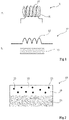
- FIG. 1 schematically represents by views A and B, two inductor embodiments
- the figure 2 represents by a sectional view, a magnetic material of the inductor illustrated in view B of the figure 1 ;
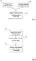
- the picture 3 represents by a block diagram a process for implementing a solution
- the figure 4 represents by a block diagram another method of implementing the solution.
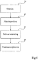
- the figure 5 represents by a block diagram a process for implementing the material illustrated in figure 2 .
- the figure 1 schematically represents by views A and B, two inductance embodiments.
- the figure 1 illustrates in view A the diagram of an inductor 11 in which a magnetic material 13 is located in the turns of a coil 15 and in view B the diagram of an inductor 17 in which the magnetic material is located under (or above ) a planar winding 15 (generally in the form of a spiral).
- Inductors are electronic compounds with the ability to store magnetic energy when a current passes through them. Inductors are used in many electronic fields and in particular in quantum computers, also called quantum computers.
- the inductors like all the electronic components located around the core of the quantum computer are brought to a very low temperature (closer to 0 K), for example to 4 K, in order to limit thermal disturbances from these components. While the usual inductors are adapted to undergo expansions, they are, on the other hand, not adapted to withstand such low temperatures.
- the picture 2 represents by a sectional view, the magnetic material 13 of the inductor 17 illustrated in view B of the figure 1 .
- the magnetic material 13 comprises an assembly of an electromagnetic material 19 and a substrate 21.
- Substrate 21 is preferably a substrate made of a semiconductor material, for example silicon.
- the substrate 21 is preferably a silicon wafer.
- the substrate 21 has, for example, a thickness of between 200 ⁇ m and 800 ⁇ m.
- the electromagnetic material 19 comprises metallic magnetic particles 23 in an electrically insulating matrix 25.
- the metallic magnetic particles 23 can be spherical, hexagonal, cubic, cylindrical or have any shape.
- Each metallic magnetic particle 23 is part of a cube or a parallelepiped whose smallest side is less than or equal to about 30 nm, that is to say whose size is less than or equal to about 30 nm.
- each metallic magnetic particle 23 is inscribed in a cube or a parallelepiped whose smallest side is less than or equal to approximately 20 nm, that is to say whose size is less than or equal to approximately 20 nm.
- each metallic magnetic particle 23 is inscribed in a cube or a parallelepiped whose smallest side is less than or equal to approximately 10 nm, that is to say whose size is less than or equal to approximately 10 nm.
- the characteristic dimension of a metallic magnetic particle 23 corresponds to the diameter of the metallic magnetic particle 23 if the latter is spherical or to the dimension of one side of the metallic magnetic particle 23 if the latter is cubic.
- the metallic magnetic particles 23 have a superparamagnetic behavior, ie their magnetization can reverse spontaneously under the influence of temperature. Thus, it can be said for simplicity of language that the metallic magnetic particles 23 are not magnetized at room temperature (that is to say approximately 25°C or 298 K) but become so at very low temperatures, typically below 4 K.
- the metallic magnetic particles 23 can be made of a material having a magnetic permeability greater than 1.5 for frequencies between 5 GHz and 50 GHz.
- the metallic magnetic particles 23 are preferably made of a material having a magnetic permeability greater than 2 and more preferably greater than 3 for frequencies between 5 GHz and 50 GHz.
- the metallic magnetic particles 23 are preferably iron (Fe), cobalt (Co) and/or nickel (Ni).
- the particles 23 are, for example, made of a material chosen from iron (Fe), cobalt (Co), nickel (Ni), and their alloys, iron carbides (Fe 3 C or Fe 5 C 2 ) or an iron nitride (Fe 2 N, Fe 4 N or Fe 16 N 2 ).
- the particles of the iron-cobalt alloy are superparamagnetic at room temperature if each of them can fit into a cube with a side less than or equal to 23 nm.
- the iron particles are superparamagnetic at room temperature if each of them can fit into a cube with a side less than or equal to 16 nm.
- the cobalt particles are superparamagnetic at ambient temperature if each of them can fit into a cube with a side less than or equal to 8 nm.
- the particles 23 can be covered with a protective film or protective shell in order to protect them against oxidation.
- the shell can be made of carbon (of the graphene, graphite or amorphous type) and/or of metal oxide (silica or alumina).
- the insulating matrix 25 is preferably composed of a material chosen from a polymer, graphene oxide or a metal oxide.
- the insulating matrix 25 is, for example, polystyrene (PS) or epoxy.
- a mode of implementation of the material 13 is described in relation to the figure 5 from a solution produced according to one or other of the processes described in relation to the figures 3 and 4 .
- the picture 3 represents by a block diagram a process for implementing a solution.
- the picture 3 illustrates the process for implementing a solution comprising the metallic magnetic particles 23 and the insulating matrix 25 in solution.
- the metallic magnetic particles 23 are, in a first step 27, dissolved in a first solvent (Solvent and particles solution). During this step, the dispersion of the metallic magnetic particles 23 in the solvent can be assisted by mechanical stirring. The dispersion of the metallic magnetic particles 23 is further assisted by sonication, ultrasonication or ultrasound.
- a dielectric polymer is optionally grafted onto the surface of the nanoparticles magnetic 23. This grafting, for example, assisted by sonication, makes it possible to ensure electrical insulation between the particles.
- the dielectric polymer is, for example, grafted in the form of a very thin layer, of the order of a few nanometers, for example of a thickness equal to approximately 4 nm.
- Step 29 the insulating matrix is dissolved in a second solvent during a step 29 (Solvent and matrix material solution).
- Step 29 can alternatively be performed before or after step 27.
- the first solvent can be different or identical to the second solvent, the first solvent and the second solvent are however miscible.
- the dissolution of the insulating matrix 25 in the second solvent can be assisted by mechanical stirring and, optionally, by ultrasound.
- the solution comprising the metallic magnetic particles 23 and the solution comprising the insulating matrix 25 are mixed (Mixing under agitation and sonication or ultrasounds), preferably under mechanical agitation and under sonication or under ultrasound .
- the insulating matrix 25 is not dissolved in step 29 and is added directly in step 31.
- the figure 4 represents by a block diagram another method of implementing the solution.
- the figure 4 illustrates a method similar to the method illustrated in picture 3 with the difference that the metallic magnetic particles 23 are, in a step 33, mixed with the insulating matrix 25 (Particles and matrix material mixing) before adding a solvent to the mixture in a step 35 (Solvent adding). Similar to the process illustrated in picture 3 , the dispersion of the particles 23 in the solvent and the dissolution of the matrix 25 in this same solvent are assisted by sonication and/or by ultrasound (step 37, Mixing under agitation and sonication or ultrasound).
- the figure 5 represents by a block diagram a process for implementing the material illustrated in picture 2 .
- figure 5 illustrates a process for implementing the material illustrated in figure 2 from the solution made in picture 3 or 4 .
- the solution is, in a first step 39, prepared according to one of the implementation methods described in relation to the figures 3 and 4 (Solution). Following step 39, the solution is deposited, during a step 41, on the surface of the substrate (21, picture 2 ). During step 41, a wet film is formed (Deposition Film). According to one embodiment, step 41 is carried out by centrifugation (spin-coating) or by puddle deposition (puddle-coating).
- step 41 is performed by ink jet (ink jet), by aerosol deposition (spray) or by injection molding (injection molding).
- the structure composed of the film and the substrate (21, figure 2 ) undergoes, during a step 43, an annealing (Solvent annealing) so as to evaporate the traces of solvent present in the film and to form the material 19.
- the annealing is preferably carried out at a temperature of the order 100°C for about 10 minutes.
- Step 43 may be followed by a step 45 of thermal compression (thermocompression) making it possible to densify the material 19 and flatten it.
- thermal compression thermal compression
- An advantage of the embodiments and modes of implementation described is that they make it possible to overcome the usual spontaneous agglomeration of submicron magnetic particles.
- Another advantage of the embodiments and modes of implementation described is that they make it possible to obtain an electromagnetic material in which the metallic magnetic particles have a homogeneous dispersion in the insulating matrix.
- Yet another advantage of the embodiments and modes of implementation described is that they make it possible to simplify the step of dispersing the particles in the insulating matrix or in the solvent and thus preserve the surface state of the particles.
Landscapes
- Engineering & Computer Science (AREA)
- Chemical & Material Sciences (AREA)
- Power Engineering (AREA)
- Health & Medical Sciences (AREA)
- Nanotechnology (AREA)
- Dispersion Chemistry (AREA)
- Life Sciences & Earth Sciences (AREA)
- Biomedical Technology (AREA)
- General Health & Medical Sciences (AREA)
- Molecular Biology (AREA)
- Organic Chemistry (AREA)
- Polymers & Plastics (AREA)
- Ceramic Engineering (AREA)
- Chemical Kinetics & Catalysis (AREA)
- Medicinal Chemistry (AREA)
- Inorganic Chemistry (AREA)
- Manufacturing & Machinery (AREA)
- Materials Engineering (AREA)
- Structural Engineering (AREA)
- Electromagnetism (AREA)
- Physics & Mathematics (AREA)
- Microelectronics & Electronic Packaging (AREA)
- Coils Or Transformers For Communication (AREA)
- Soft Magnetic Materials (AREA)
Abstract
Description
- La présente description concerne de façon générale les inductances et plus précisément les inductances destinées aux ordinateurs quantiques. La présente description concerne plus particulièrement un matériau électromagnétique pour la réalisation d'inductances fonctionnant à basses températures pour dispositifs quantiques.
- Dans les ordinateurs quantiques, les inductances comme l'ensemble des composants électroniques situés autour du coeur de l'ordinateur quantique sont portés à très basse température (au plus proche de 0 K) afin de limiter les perturbations thermiques issues de ces composants. Les inductances connues qui se rapprochent le plus du cahier des charges lié aux fréquences de travail des ordinateurs quantiques sont, à ce jour, les inductances développées entre autres pour les applications liées aux télécommunications 5G. Les inductances utilisées actuellement dans la technologie 5G sont réalisées en couches minces sur silicium avec les moyens de la microélectronique actuelle. Elles sont constituées d'une multitude de couches minces en matériaux diélectriques (oxydes et nitrures métalliques, polymères ...), conducteurs (Al, Cu, Au, Ni) et magnétiques (films amorphes ou nanocristallins à base de Fe, Co, Ni). Toutes ces couches sont déposées sur un substrat (Si, SOI, verre, céramique etc.). Ces inductances sont conçues pour fonctionner à des températures comprises entre -40°C et +85°C et peuvent supporter des températures de fabrication jusqu'à 400°C. Mais si la température d'utilisation se rapproche de 0K, comme dans le cas des applications quantiques, le composant subira des forces de compression très importantes (puisqu'il a été dilaté au moment de sa fabrication) provoquant généralement la décohésion des couches, des ruptures de connections électriques et même des fracturations du substrat.
- Dans des technologies hybrides plus émergentes, on tend à réduire le nombre de couches minces à fort bilan thermique et à les remplacer par des polymères fonctionnels qui se déposent à température ambiante. Par exemple, le matériau magnétique en multicouches peut être remplacé par un polymère épais contenant des particules ferromagnétiques qui fait aussi office d'isolant électrique avec les spires de l'inductance et de résine d'encapsulation. La fiabilité mécanique et électrique face aux variations thermiques, notamment, négatives est améliorée. De plus, les polymères résistent très bien aux très basses températures.
- Cependant, pour obtenir des fréquences d'utilisation élevées (5 à 10 GHz), il est nécessaire de recourir à des particules ferromagnétiques submicroniques par exemple inférieures à 100 nm pour limiter les pertes au-delà de 1 GHz.
- La manipulation de ces particules ferromagnétiques est extrêmement délicate parce qu'elles conservent une aimantation rémanente à la température ambiante. Elles agissent par conséquent comme de très petits « aimants » qui s'attirent tête-bêche et se collent l'une à l'autre. En pratique, ce type de nanoparticules s'agglomèrent spontanément et il est particulièrement difficile de les séparer. Cela constitue des agrégats conducteurs au sein du polymère qui génèrent les pertes en excès à partir de 1 GHz qui n'est pas souhaitable.
- Il existe un besoin d'améliorer les inductances pour les ordinateurs quantiques.
- Un mode de réalisation pallie tout ou partie des inconvénients des inductances des ordinateurs quantiques connus.
- Un mode de réalisation prévoit plus particulièrement un matériau électromagnétique adapté à la réalisation d'inductances.
- Un mode de réalisation prévoit un matériau électromagnétique pour inductance à fonctionnement à des températures cryogéniques comportant, dans une matrice électriquement isolante, des nanoparticules métalliques à comportement superparamagnétique de taille inférieure ou égale à 30 nm et ayant une perméabilité magnétique supérieure ou égale à 1,5 pour une fréquence comprise entre 5 GHz et 50 GHz.
- Selon un mode de réalisation, chaque particule s'inscrit dans un cube ou un parallélépipède d'une taille inférieure ou égale à 20 nm.
- Selon un mode de réalisation, chaque particule s'inscrit dans un cube ou un parallélépipède d'une taille inférieure ou égale à 10 nm.
- Selon un mode de réalisation, la perméabilité magnétique de chaque particule est supérieure à 3.
- Selon un mode de réalisation, la matrice est un polymère.
- Selon un mode de réalisation, la matrice est un oxyde métallique.
- Selon un mode de réalisation, la matrice est un oxyde de graphène.
- Selon un mode de réalisation, les particules comprennent du fer, du cobalt, du nickel, et/ou un alliage de ces métaux.
- Selon un mode de réalisation, les particules sont les carbures ou nitrures de fer tels que Fe3C, Fe5C2, Fe2N, Fe4N, Fe16N2.
- Selon un mode de réalisation, les particules sont recouvertes d'une couche superficielle de protection en matériau inorganique ou organique tels le graphène, le graphite, le carbone amorphe, un oxyde métallique ou un polymère.
- Un mode de réalisation prévoit un élément inductif comportant un matériau électromagnétique, tel que décrit ci-avant, caractérisé en ce sens que la valeur d'inductance est plus élevée (par exemple de 10 %, 30 %, 50 %, 100 %, 200 %) à une température inférieure ou égale à 4 K qu'à la température ambiante.
- Selon un mode de réalisation, l'élément inductif fonctionne à une température inférieure ou égale à 4K.
- Ces caractéristiques et avantages, ainsi que d'autres, seront exposés en détail dans la description suivante de modes de réalisation particuliers faite à titre non limitatif en relation avec les figures jointes parmi lesquelles :
- la
figure 1 représente schématiquement par des vues A et B, deux modes de réalisation d'inductance ; - la
figure 2 représente par une vue en coupe, un matériau magnétique de l'inductance illustrée en vue B de lafigure 1 ; - la
figure 3 représente par un schéma bloc un procédé de mise en oeuvre d'une solution ; - la
figure 4 représente par un schéma bloc un autre procédé de mise en oeuvre de la solution ; et - la
figure 5 représente par un schéma bloc un procédé de mise en oeuvre du matériau illustré enfigure 2 . - De mêmes éléments ont été désignés par de mêmes références dans les différentes figures. En particulier, les éléments structurels et/ou fonctionnels communs aux différents modes de réalisation peuvent présenter les mêmes références et peuvent disposer de propriétés structurelles, dimensionnelles et matérielles identiques.
- Par souci de clarté, seuls les étapes et éléments utiles à la compréhension des modes de réalisation décrits ont été représentés et sont détaillés. En particulier, les spires de bobine, leur forme, leur dimension et leur matériau n'a pas été détaillé, le matériau électromagnétique décrit ci-après étant compatible avec les bobines usuelles.
- Sauf précision contraire, lorsque l'on fait référence à deux éléments connectés entre eux, cela signifie directement connectés sans éléments intermédiaires autres que des conducteurs, et lorsque l'on fait référence à deux éléments reliés (en anglais "coupled") entre eux, cela signifie que ces deux éléments peuvent être connectés ou être reliés par l'intermédiaire d'un ou plusieurs autres éléments.
- Dans la description qui suit, lorsque l'on fait référence à des qualificatifs de position absolue, tels que les termes "avant", "arrière", "haut", "bas", "gauche", "droite", etc., ou relative, tels que les termes "dessus", "dessous", "supérieur", "inférieur", etc., ou à des qualificatifs d'orientation, tels que les termes "horizontal", "vertical", etc., il est fait référence sauf précision contraire à l'orientation des figures.
- Sauf précision contraire, les expressions "environ", "approximativement", "sensiblement", et "de l'ordre de" signifient à 10 % près, de préférence à 5 % près.
- La
figure 1 représente schématiquement par des vues A et B, deux modes de réalisation d'inductance. - Plus particulièrement, la
figure 1 illustre en vue A le schéma d'une inductance 11 dans laquelle un matériau magnétique 13 est situé dans les spires d'une bobine 15 et en vue B le schéma d'une inductance 17 dans laquelle le matériau magnétique est situé sous (ou au dessus) un enroulement plan 15 (en général, sous forme de spirale). - Les inductances sont des composés électroniques ayant la capacité de stocker de l'énergie magnétique lorsqu'ils sont traversés par un courant. Les inductances sont utilisées dans de nombreux domaines électroniques et notamment dans les calculateurs quantiques, également appelés ordinateurs quantiques.
- Comme indiqué précédemment, dans les ordinateurs quantiques, les inductances comme l'ensemble des composants électroniques situés autour du coeur de l'ordinateur quantique sont portés à très basse température (au plus proche de 0 K), par exemple à 4 K, afin de limiter les perturbations thermiques issues de ces composants. Alors que les inductances usuelles sont adaptées à subir des dilatations, elles ne sont, en revanche, pas adaptées à résister à des températures aussi basses.
- La
figure 2 représente par une vue en coupe, le matériau magnétique 13 de l'inductance 17 illustrée en vue B de lafigure 1 . - Plus particulièrement, le matériau magnétique 13 comprend un assemblage d'un matériau électromagnétique 19 et d'un substrat 21.
- Le substrat 21 est, de préférence, un substrat en un matériau semiconducteur, par exemple, en silicium. Le substrat 21 est de préférence, une plaquette (wafer) en silicium. Le substrat 21 a, par exemple, une épaisseur comprise entre 200 µm et 800 µm.
- Le matériau électromagnétique 19 comprend des particules magnétiques métalliques 23 dans une matrice électriquement isolante 25.
- Les particules magnétiques métalliques 23 peuvent être sphériques, hexagonales, cubiques, cylindriques ou avoir une forme quelconque. Chaque particule magnétique métallique 23 s'inscrit dans un cube ou un parallélépipède dont le plus petit côté est inférieur ou égal à environ 30 nm, c'est-à-dire dont la taille est inférieure ou égale à environ 30 nm. De préférence, chaque particule magnétique métallique 23 s'inscrit dans un cube ou un parallélépipède dont le plus petit côté est inférieur ou égal à environ 20 nm, c'est-à-dire dont la taille est inférieure ou égale à environ 20 nm. Plus préférentiellement, chaque particule magnétique métallique 23 s'inscrit dans un cube ou un parallélépipède dont le plus petit côté est inférieur ou égal à environ 10 nm, c'est-à-dire dont la taille est inférieure ou égale à environ 10 nm. A titre d'exemple, la dimension caractéristique d'une particule magnétique métallique 23 correspond au diamètre de la particule magnétique métallique 23 si celle-ci est sphérique ou à la dimension d'un côté de la particule magnétique métallique 23 si celle-ci est cubique.
- Les particules magnétiques métalliques 23 ont un comportement superparamagnétique, c'est-à-dire que leur aimantation peut se renverser spontanément sous l'influence de la température. Ainsi, on peut dire par simplification de langage que les particules magnétiques métalliques 23 ne sont pas aimantées à température ambiante (c'est-à-dire environ 25 °C ou 298 K) mais le deviennent à des températures très faibles, typiquement inférieures à 4 K.
- Les particules magnétiques métalliques 23 peuvent être en un matériau ayant une perméabilité magnétique supérieure à 1,5 pour des fréquences comprises entre 5 GHz et 50 GHz. Les particules magnétiques métalliques 23 sont, de préférence, en un matériau ayant une perméabilité magnétique supérieure à 2 et plus préférentiellement supérieure à 3 pour des fréquences comprises entre 5 GHz et 50 GHz.
- Les particules magnétiques métalliques 23 sont, de préférence, en fer (Fe), en cobalt (Co) et/ou en nickel (Ni). Les particules 23 sont, par exemple, en un matériau choisi parmi le fer (Fe), le cobalt (Co), le nickel (Ni), et leurs alliages, les carbures de fer (Fe3C ou Fe5C2) ou un nitrure de fer (Fe2N, Fe4N ou Fe16N2).
- A titre d'exemple, les particules de l'alliage fer-cobalt (FeCo) sont superparamagnétiques à température ambiante si chacune d'entre elle peut s'inscrire dans un cube de côté inférieur ou égal à 23 nm. Selon un autre exemple, les particules de fer sont superparamagnétiques à température ambiante si chacune d'entre elle peut s'inscrire dans un cube de côté inférieur ou égal à 16 nm. Selon encore un autre exemple les particules de cobalt sont superparamagnétiques à température ambiante si chacune d'entre elle peut s'inscrire dans un cube de côté inférieur ou égal à 8 nm.
- Les particules 23 peuvent être recouvertes d'un film de protection ou coquille de protection afin de les protéger contre l'oxydation. A titre d'exemple, la coquille peut être en carbone (de type graphène, graphite ou amorphe) et/ou en oxyde métallique (silice ou alumine).
- La matrice isolante 25 est, de préférence, composée d'un matériau choisi parmi un polymère, de l'oxyde de graphène ou un oxyde métallique. La matrice isolante 25 est, par exemple, en polystyrène (PS) ou en époxy.
- Un mode de mise en oeuvre du matériau 13 est décrit en relation avec la
figure 5 à partir d'une solution fabriquée selon l'un ou l'autre des procédés décrits en relation avec lesfigures 3 et 4 . - La
figure 3 représente par un schéma bloc un procédé de mise en oeuvre d'une solution. - Plus particulièrement, la
figure 3 illustre le procédé de mise en oeuvre d'une solution comprenant les particules magnétiques métalliques 23 et la matrice isolante 25 en solution. - Les particules magnétiques métalliques 23 sont, dans une première étape 27 mises en solution dans un premier solvant (Solvent and particules solution) . Lors de cette étape, la dispersion des particules magnétiques métalliques 23 dans le solvant peut être assistée par une agitation mécanique. La dispersion des particules magnétiques métalliques 23 est, en outre, assistée par sonication, ultrasonication ou ultrasons.
- Un avantage qui apparaît est que la dispersion des particules magnétiques métalliques 23 est facilitée du fait que, à température ambiante, ces dernières ne sont pas aimantées. Les particules 23 se regroupent alors peu en agrégats et peuvent être mieux séparés avec une puissance et un temps de sonication moindre (c'est-à-dire une puissance comprise entre 0,5 W et 50 W contre une puissance de 500 W pour casser des agrégats de particules magnétiques). Lorsque la puissance et le temps de sonication est important (quelques centaines de Watts pendant plusieurs dizaines de minutes), les particules 23 peuvent être endommagées.
- Lors de l'étape 27, un polymère diélectrique est, optionnellement, greffé à la surface des nanoparticules magnétiques 23. Ce greffage, par exemple, assisté par sonication, permet d'assurer l'isolation électrique entre les particules. Le polymère diélectrique, est, par exemple, greffé sous forme d'une très fine couche, de l'ordre de quelques nanomètres, par exemple d'une épaisseur égale à environ 4 nm.
- En parallèle de l'étape 27, la matrice isolante est mise en solution dans un deuxième solvant lors d'une étape 29 (Solvent and matrix material solution). L'étape 29 peut, en variante, être réalisée avant ou après l'étape 27.
- Le premier solvant peut être différent ou identique du deuxième solvant, le premier solvant et le deuxième solvant sont toutefois miscibles.
- Lors de l'étape 29, la dissolution de la matrice isolante 25 dans le deuxième solvant peut être assistée par agitation mécanique et, éventuellement, par ultrasons.
- Dans une étape 31 postérieure aux étapes 27 et 29, la solution comprenant les particules magnétiques métalliques 23 et la solution comprenant la matrice isolante 25 sont mélangées (Mixing under agitation and sonication or ultrasounds), de préférence sous agitation mécanique et sous sonication ou sous ultrasons.
- En variante, la matrice isolante 25 n'est pas mise en solution dans l'étape 29 et est ajoutée directement à l'étape 31.
- La
figure 4 représente par un schéma bloc un autre procédé de mise en oeuvre de la solution. - La
figure 4 illustre un procédé similaire au procédé illustré enfigure 3 à la différence près que les particules magnétiques métalliques 23 sont, dans une étape 33 mélangées avec la matrice isolante 25 (Particles and matrix material mixing) avant d'ajouter au mélange un solvant dans une étape 35 (Solvent adding). Similairement au procédé illustré enfigure 3 , la dispersion des particules 23 dans le solvant et la dissolution de la matrice 25 dans ce même solvant sont assistées par sonication et/ou par ultrasons (étape 37, Mixing under agitation and sonication or ultrasonds). - Ainsi, alors que l'on n'aurait pas tendance à utiliser ces nanoparticules au comportement superparamagnétique pour réaliser des éléments inductifs en raison de leur absence d'efficacité (c'est-à-dire n'ayant pas de contribution à l'inductance) à température ambiante qui est habituellement le comportement évalué, on prévoit ici de tirer profit de leur changement de comportement entre la température ambiante et les températures proches du zéro Kelvin afin de bénéficier des autres caractéristiques de ces nanoparticules lorsqu'elles sont à température ambiante ou supérieure, et en particulier la facilité donnée de les maintenir en suspension à température ambiante, et de les disperser de manière homogène, c'est-à-dire sans agrégats.
- La
figure 5 représente par un schéma bloc un procédé de mise en oeuvre du matériau illustré enfigure 2 . - Plus particulièrement, la
figure 5 illustre un procédé de mise en oeuvre du matériau illustré enfigure 2 à partir de la solution réalisée enfigure 3 ou 4 . - La solution est, dans une première étape 39, préparée selon l'un des procédés de mise en oeuvre décrits en relation avec les
figures 3 et 4 (Solution). A la suite de l'étape 39, la solution est déposée, lors d'une étape 41, à la surface du substrat (21,figure 2 ). Lors de l'étape 41, un film humide est formé (Film déposition). Selon un mode de réalisation l'étape 41 est réalisée par centrifugation (spin-coating) ou par dépôt à la flaque (puddle-coating). - Selon un autre mode de réalisation, l'étape 41 est réalisée par jet d'encre (ink jet), par dépôt par aérosol (spray) ou par moulage par injection (injection molding).
- A la suite de l'étape 41, la structure composée du film et du substrat (21,
figure 2 ) subit, lors d'une étape 43, un recuit (Solvant annealing) de façon à évaporer les traces de solvant présentes dans le film et à former le matériau 19. Le recuit est, de préférence, réalisé à une température de l'ordre de 100 °C pendant environ 10 minutes. - L'étape 43 peut être suivie par une étape 45 de compression thermique (thermocompression) permettant de densifier le matériau 19 et l'aplanir.
- Un avantage des modes de réalisation et des modes de mise en oeuvre décrits est qu'ils permettent de s'affranchir de l'agglomération spontanée usuelle des particules magnétiques submicroniques.
- Un autre avantage des modes de réalisation et des modes de mise en oeuvre décrits est qu'ils permettent d'obtenir un matériau électromagnétique dans lequel les particules magnétiques métalliques ont une dispersion homogène dans la matrice isolante.
- Encore un autre avantage des modes de réalisation et des modes de mise en oeuvre décrits est qu'ils permettent de simplifier l'étape de dispersion des particules dans la matrice isolante ou dans le solvant et ainsi préserver l'état de surface des particules.
- Encore un autre avantage des modes de réalisation et des modes de mise en oeuvre décrits est qu'ils permettent d'apporter au matériau électromagnétique une meilleure isolation électrique et de réduire les pertes électromagnétiques en comparaison aux matériaux usuellement utilisés dans les inductances.
- Divers modes de réalisation et variantes ont été décrits. La personne du métier comprendra que certaines caractéristiques de ces divers modes de réalisation et variantes pourraient être combinées, et d'autres variantes apparaîtront à la personne du métier.
- Enfin, la mise en oeuvre pratique des modes de réalisation et variantes décrits est à la portée de la personne du métier à partir des indications fonctionnelles données ci-dessus.
Claims (12)
- Matériau électromagnétique (13) pour inductance à fonctionnement à des températures cryogéniques comportant, dans une matrice électriquement isolante (25), des nanoparticules métalliques (23) à comportement superparamagnétique de taille inférieure ou égale à 30 nm et ayant une perméabilité magnétique supérieure ou égale à 1,5 pour une fréquence comprise entre 5 GHz et 50 GHz.
- Matériau électromagnétique selon la revendication 1, dans lequel chaque particule (23) s'inscrit dans un cube ou un parallélépipède d'une taille inférieure ou égale à 20 nm.
- Matériau électromagnétique selon la revendication 1 ou 2, dans lequel chaque particule (23) s'inscrit dans un cube ou un parallélépipède d'une taille inférieure ou égale à 10 nm.
- Matériau électromagnétique selon l'une quelconque des revendications 1 à 3, dans lequel la perméabilité magnétique de chaque particule (23) est supérieure à 3.
- Matériau électromagnétique selon l'une quelconque des revendications 1 à 4, dans lequel la matrice (25) est un polymère.
- Matériau électromagnétique selon l'une quelconque des revendications 1 à 4, dans lequel la matrice (25) est un oxyde métallique.
- Matériau électromagnétique selon l'une quelconque des revendications 1 à 4, dans lequel la matrice (25) est un oxyde de graphène.
- Matériau électromagnétique selon l'une quelconque des revendications 1 à 7, dans lequel les particules (25) comprennent du fer, du cobalt, du nickel, et/ou un alliage de ces métaux.
- Matériau électromagnétique selon la revendication 8, dans lequel les particules (23) sont les carbures ou nitrures de fer tels que Fe3C, Fe5C2, Fe2N, Fe4N, Fe16N2.
- Matériau électromagnétique (13) selon l'une des revendications 1 à 9, dans lequel les particules (23) sont recouvertes d'une couche superficielle de protection en matériau inorganique ou organique tels le graphène, le graphite, le carbone amorphe, un oxyde métallique ou un polymère.
- Elément inductif (11) comportant un matériau électromagnétique (13) selon l'une quelconque des revendications 1 à 10, caractérisé en ce sens que la valeur d'inductance est plus élevée (par exemple de 10 %, 30 %, 50 %, 100 %, 200 %) à une température inférieure ou égale à 4 K qu'à la température ambiante.
- Elément inductif (11) selon la revendication 11, fonctionnant à une température inférieure ou égale à 4K.
Applications Claiming Priority (1)
| Application Number | Priority Date | Filing Date | Title |
|---|---|---|---|
| FR2012856A FR3117260B1 (fr) | 2020-12-08 | 2020-12-08 | Matériau électromagnétique et inductance pour les basses températures |
Publications (2)
| Publication Number | Publication Date |
|---|---|
| EP4012728A1 true EP4012728A1 (fr) | 2022-06-15 |
| EP4012728B1 EP4012728B1 (fr) | 2024-02-07 |
Family
ID=74669037
Family Applications (1)
| Application Number | Title | Priority Date | Filing Date |
|---|---|---|---|
| EP21212053.9A Active EP4012728B1 (fr) | 2020-12-08 | 2021-12-02 | Matériau électromagnétique et inductance pour les basses températures |
Country Status (4)
| Country | Link |
|---|---|
| US (1) | US12424361B2 (fr) |
| EP (1) | EP4012728B1 (fr) |
| CN (1) | CN114628103A (fr) |
| FR (1) | FR3117260B1 (fr) |
Citations (4)
| Publication number | Priority date | Publication date | Assignee | Title |
|---|---|---|---|---|
| FR2953028A1 (fr) * | 2009-11-26 | 2011-05-27 | Billanco | Capteur de circulation de champs magnetiques equipe d'un moyen de verification, et procede de verification d'un tel capteur. |
| US20120012778A1 (en) * | 2008-12-19 | 2012-01-19 | Richard David Tilley | Magnetic Nanoparticles |
| US20120229238A1 (en) * | 2009-11-09 | 2012-09-13 | Ferrotec Corporation | Magnetic Member and Electronic Component |
| US20130342069A1 (en) * | 2012-06-21 | 2013-12-26 | Toyota Motor Engineering & Manufacturing Na | Iron oxide and silica magnetic core |
Family Cites Families (6)
| Publication number | Priority date | Publication date | Assignee | Title |
|---|---|---|---|---|
| US5574961A (en) * | 1985-01-16 | 1996-11-12 | The United States Of America As Represented By The Secretary Of The Navy | Phase-separated material (U) |
| US4824587A (en) * | 1985-03-18 | 1989-04-25 | The Dow Chemical Company | Composites of coercive particles and superparamagnetic particles |
| JPH08508721A (ja) * | 1993-03-17 | 1996-09-17 | シリカゲル ゲス.エム.ビー.エイチ | 超常磁性粒子、その製法及びその用途 |
| JP2007036183A (ja) * | 2005-06-21 | 2007-02-08 | Fujifilm Holdings Corp | 磁性粒子の製造方法、磁性粒子、磁気記録媒体 |
| ES2365082B1 (es) * | 2010-03-08 | 2012-08-08 | Consejo Superior De Investigaciones Científicas (Csic) | Procedimiento de obtencion de materiales con comportamiento superparamagnetico |
| CN103214042B (zh) * | 2013-04-27 | 2015-11-18 | 中国科学院金属研究所 | 一种超顺磁稀土金属间化合物纳米颗粒及其制备方法 |
-
2020
- 2020-12-08 FR FR2012856A patent/FR3117260B1/fr active Active
-
2021
- 2021-12-02 EP EP21212053.9A patent/EP4012728B1/fr active Active
- 2021-12-06 US US17/543,693 patent/US12424361B2/en active Active
- 2021-12-08 CN CN202111490950.3A patent/CN114628103A/zh active Pending
Patent Citations (4)
| Publication number | Priority date | Publication date | Assignee | Title |
|---|---|---|---|---|
| US20120012778A1 (en) * | 2008-12-19 | 2012-01-19 | Richard David Tilley | Magnetic Nanoparticles |
| US20120229238A1 (en) * | 2009-11-09 | 2012-09-13 | Ferrotec Corporation | Magnetic Member and Electronic Component |
| FR2953028A1 (fr) * | 2009-11-26 | 2011-05-27 | Billanco | Capteur de circulation de champs magnetiques equipe d'un moyen de verification, et procede de verification d'un tel capteur. |
| US20130342069A1 (en) * | 2012-06-21 | 2013-12-26 | Toyota Motor Engineering & Manufacturing Na | Iron oxide and silica magnetic core |
Also Published As
| Publication number | Publication date |
|---|---|
| FR3117260A1 (fr) | 2022-06-10 |
| CN114628103A (zh) | 2022-06-14 |
| FR3117260B1 (fr) | 2022-11-04 |
| US20220181053A1 (en) | 2022-06-09 |
| US12424361B2 (en) | 2025-09-23 |
| EP4012728B1 (fr) | 2024-02-07 |
Similar Documents
| Publication | Publication Date | Title |
|---|---|---|
| EP3252782B1 (fr) | Nanocomposite et procédé d'obtention associé | |
| Zeng et al. | Bimagnetic core/shell FePt/Fe3O4 nanoparticles | |
| WO2007010137A1 (fr) | Dispositif radiofrequence avec element magnetique procede de fabrication d'un tel element magnetique | |
| US8866243B2 (en) | Ferromagnetic tunnel junction structure and magnetoresistive element using the same | |
| EP1187149A1 (fr) | Microcomposant du type micro-inductance ou micro-transformateur | |
| Llamosa Pérez et al. | Thermal diffusion at nanoscale: from CoAu alloy nanoparticles to Co@ Au core/shell structures | |
| WO2012109519A2 (fr) | Élément magnétique à anisotropie hors du plan améliorée pour applications spintroniques | |
| Dong et al. | Enhanced thermal stability and magnetic properties in NaCl-Type FePt–MnO binary nanocrystal superlattices | |
| FR2620853A1 (fr) | Materiau magnetique composite et son procede de fabrication | |
| EP3696834A1 (fr) | Capacite metal-polymere comprenant un film dielectrique a forte constante dielectrique et a fort champ de claquage | |
| US20110195277A1 (en) | High density magnetic recording medium and manufacturing method thereof | |
| WO1999027379A1 (fr) | Capteur de champ magnetique et procede de fabrication de ce capteur | |
| EP4012728B1 (fr) | Matériau électromagnétique et inductance pour les basses températures | |
| JP5136751B2 (ja) | FePtナノ粒子の製造方法、及びFePt磁性ナノ粒子配列体を有する磁気記録媒体の製造方法 | |
| EP3895188B1 (fr) | Procédé de fabrication d'un aimant permanent ou doux | |
| FR3009884A1 (fr) | Procede de fabrication d'un composant electromagnetique monolithique et composant magnetique monolithique associe | |
| Holmes et al. | Cobalt-based Heusler alloys for spin-injection devices | |
| EP2278664A1 (fr) | Corps main gauche, dispositif de guidage d'ondes et antenne utilisant ce corps, procédé de fabrication de ce corps | |
| CN1422977A (zh) | 用共溅射法沉积赫斯勒合金薄膜的方法 | |
| EP2143309B1 (fr) | Procede de realisation d'un module d'alimentation a base de materiau magnetique | |
| WO2013156426A1 (fr) | Dispositif injecteur de spins comportant une couche de protection en son centre | |
| JP2001202611A (ja) | 磁気記録媒体、磁気記録媒体製造方法、および情報再生装置 | |
| JP7520434B2 (ja) | 規則化合金強磁性ナノワイヤ構造体及びその製造方法 | |
| FR2812756A1 (fr) | Microcomposant du type micro-inductance ou micro- transformateur | |
| EP1989716B1 (fr) | Semi-conducteur ferromagnetique, son procede de fabrication, composants l'incorporant et utilisations de ce semi-conducteur s'y rapportant |
Legal Events
| Date | Code | Title | Description |
|---|---|---|---|
| PUAI | Public reference made under article 153(3) epc to a published international application that has entered the european phase |
Free format text: ORIGINAL CODE: 0009012 |
|
| STAA | Information on the status of an ep patent application or granted ep patent |
Free format text: STATUS: REQUEST FOR EXAMINATION WAS MADE |
|
| 17P | Request for examination filed |
Effective date: 20211202 |
|
| AK | Designated contracting states |
Kind code of ref document: A1 Designated state(s): AL AT BE BG CH CY CZ DE DK EE ES FI FR GB GR HR HU IE IS IT LI LT LU LV MC MK MT NL NO PL PT RO RS SE SI SK SM TR |
|
| RIC1 | Information provided on ipc code assigned before grant |
Ipc: H01F 41/24 20060101ALN20230714BHEP Ipc: H01F 41/16 20060101ALN20230714BHEP Ipc: H01F 17/04 20060101ALI20230714BHEP Ipc: H01F 3/08 20060101ALI20230714BHEP Ipc: H01F 1/00 20060101AFI20230714BHEP |
|
| GRAP | Despatch of communication of intention to grant a patent |
Free format text: ORIGINAL CODE: EPIDOSNIGR1 |
|
| STAA | Information on the status of an ep patent application or granted ep patent |
Free format text: STATUS: GRANT OF PATENT IS INTENDED |
|
| RIC1 | Information provided on ipc code assigned before grant |
Ipc: H01F 41/24 20060101ALN20230810BHEP Ipc: H01F 41/16 20060101ALN20230810BHEP Ipc: H01F 17/04 20060101ALI20230810BHEP Ipc: H01F 3/08 20060101ALI20230810BHEP Ipc: H01F 1/00 20060101AFI20230810BHEP |
|
| INTG | Intention to grant announced |
Effective date: 20230828 |
|
| RIN1 | Information on inventor provided before grant (corrected) |
Inventor name: VIALA, BERNARD |
|
| GRAS | Grant fee paid |
Free format text: ORIGINAL CODE: EPIDOSNIGR3 |
|
| GRAA | (expected) grant |
Free format text: ORIGINAL CODE: 0009210 |
|
| STAA | Information on the status of an ep patent application or granted ep patent |
Free format text: STATUS: THE PATENT HAS BEEN GRANTED |
|
| AK | Designated contracting states |
Kind code of ref document: B1 Designated state(s): AL AT BE BG CH CY CZ DE DK EE ES FI FR GB GR HR HU IE IS IT LI LT LU LV MC MK MT NL NO PL PT RO RS SE SI SK SM TR |
|
| REG | Reference to a national code |
Ref country code: GB Ref legal event code: FG4D Free format text: NOT ENGLISH |
|
| REG | Reference to a national code |
Ref country code: CH Ref legal event code: EP |
|
| REG | Reference to a national code |
Ref country code: IE Ref legal event code: FG4D Free format text: LANGUAGE OF EP DOCUMENT: FRENCH |
|
| REG | Reference to a national code |
Ref country code: DE Ref legal event code: R096 Ref document number: 602021009190 Country of ref document: DE |
|
| REG | Reference to a national code |
Ref country code: LT Ref legal event code: MG9D |
|
| REG | Reference to a national code |
Ref country code: NL Ref legal event code: MP Effective date: 20240207 |
|
| PG25 | Lapsed in a contracting state [announced via postgrant information from national office to epo] |
Ref country code: IS Free format text: LAPSE BECAUSE OF FAILURE TO SUBMIT A TRANSLATION OF THE DESCRIPTION OR TO PAY THE FEE WITHIN THE PRESCRIBED TIME-LIMIT Effective date: 20240607 |
|
| PG25 | Lapsed in a contracting state [announced via postgrant information from national office to epo] |
Ref country code: LT Free format text: LAPSE BECAUSE OF FAILURE TO SUBMIT A TRANSLATION OF THE DESCRIPTION OR TO PAY THE FEE WITHIN THE PRESCRIBED TIME-LIMIT Effective date: 20240207 |
|
| PG25 | Lapsed in a contracting state [announced via postgrant information from national office to epo] |
Ref country code: GR Free format text: LAPSE BECAUSE OF FAILURE TO SUBMIT A TRANSLATION OF THE DESCRIPTION OR TO PAY THE FEE WITHIN THE PRESCRIBED TIME-LIMIT Effective date: 20240508 |
|
| REG | Reference to a national code |
Ref country code: AT Ref legal event code: MK05 Ref document number: 1655894 Country of ref document: AT Kind code of ref document: T Effective date: 20240207 |
|
| PG25 | Lapsed in a contracting state [announced via postgrant information from national office to epo] |
Ref country code: HR Free format text: LAPSE BECAUSE OF FAILURE TO SUBMIT A TRANSLATION OF THE DESCRIPTION OR TO PAY THE FEE WITHIN THE PRESCRIBED TIME-LIMIT Effective date: 20240207 Ref country code: NL Free format text: LAPSE BECAUSE OF FAILURE TO SUBMIT A TRANSLATION OF THE DESCRIPTION OR TO PAY THE FEE WITHIN THE PRESCRIBED TIME-LIMIT Effective date: 20240207 Ref country code: RS Free format text: LAPSE BECAUSE OF FAILURE TO SUBMIT A TRANSLATION OF THE DESCRIPTION OR TO PAY THE FEE WITHIN THE PRESCRIBED TIME-LIMIT Effective date: 20240507 |
|
| PG25 | Lapsed in a contracting state [announced via postgrant information from national office to epo] |
Ref country code: ES Free format text: LAPSE BECAUSE OF FAILURE TO SUBMIT A TRANSLATION OF THE DESCRIPTION OR TO PAY THE FEE WITHIN THE PRESCRIBED TIME-LIMIT Effective date: 20240207 |
|
| PG25 | Lapsed in a contracting state [announced via postgrant information from national office to epo] |
Ref country code: AT Free format text: LAPSE BECAUSE OF FAILURE TO SUBMIT A TRANSLATION OF THE DESCRIPTION OR TO PAY THE FEE WITHIN THE PRESCRIBED TIME-LIMIT Effective date: 20240207 |
|
| PG25 | Lapsed in a contracting state [announced via postgrant information from national office to epo] |
Ref country code: RS Free format text: LAPSE BECAUSE OF FAILURE TO SUBMIT A TRANSLATION OF THE DESCRIPTION OR TO PAY THE FEE WITHIN THE PRESCRIBED TIME-LIMIT Effective date: 20240507 Ref country code: NO Free format text: LAPSE BECAUSE OF FAILURE TO SUBMIT A TRANSLATION OF THE DESCRIPTION OR TO PAY THE FEE WITHIN THE PRESCRIBED TIME-LIMIT Effective date: 20240507 Ref country code: NL Free format text: LAPSE BECAUSE OF FAILURE TO SUBMIT A TRANSLATION OF THE DESCRIPTION OR TO PAY THE FEE WITHIN THE PRESCRIBED TIME-LIMIT Effective date: 20240207 Ref country code: LT Free format text: LAPSE BECAUSE OF FAILURE TO SUBMIT A TRANSLATION OF THE DESCRIPTION OR TO PAY THE FEE WITHIN THE PRESCRIBED TIME-LIMIT Effective date: 20240207 Ref country code: IS Free format text: LAPSE BECAUSE OF FAILURE TO SUBMIT A TRANSLATION OF THE DESCRIPTION OR TO PAY THE FEE WITHIN THE PRESCRIBED TIME-LIMIT Effective date: 20240607 Ref country code: HR Free format text: LAPSE BECAUSE OF FAILURE TO SUBMIT A TRANSLATION OF THE DESCRIPTION OR TO PAY THE FEE WITHIN THE PRESCRIBED TIME-LIMIT Effective date: 20240207 Ref country code: GR Free format text: LAPSE BECAUSE OF FAILURE TO SUBMIT A TRANSLATION OF THE DESCRIPTION OR TO PAY THE FEE WITHIN THE PRESCRIBED TIME-LIMIT Effective date: 20240508 Ref country code: FI Free format text: LAPSE BECAUSE OF FAILURE TO SUBMIT A TRANSLATION OF THE DESCRIPTION OR TO PAY THE FEE WITHIN THE PRESCRIBED TIME-LIMIT Effective date: 20240207 Ref country code: ES Free format text: LAPSE BECAUSE OF FAILURE TO SUBMIT A TRANSLATION OF THE DESCRIPTION OR TO PAY THE FEE WITHIN THE PRESCRIBED TIME-LIMIT Effective date: 20240207 Ref country code: BG Free format text: LAPSE BECAUSE OF FAILURE TO SUBMIT A TRANSLATION OF THE DESCRIPTION OR TO PAY THE FEE WITHIN THE PRESCRIBED TIME-LIMIT Effective date: 20240207 Ref country code: AT Free format text: LAPSE BECAUSE OF FAILURE TO SUBMIT A TRANSLATION OF THE DESCRIPTION OR TO PAY THE FEE WITHIN THE PRESCRIBED TIME-LIMIT Effective date: 20240207 |
|
| PG25 | Lapsed in a contracting state [announced via postgrant information from national office to epo] |
Ref country code: PL Free format text: LAPSE BECAUSE OF FAILURE TO SUBMIT A TRANSLATION OF THE DESCRIPTION OR TO PAY THE FEE WITHIN THE PRESCRIBED TIME-LIMIT Effective date: 20240207 Ref country code: PT Free format text: LAPSE BECAUSE OF FAILURE TO SUBMIT A TRANSLATION OF THE DESCRIPTION OR TO PAY THE FEE WITHIN THE PRESCRIBED TIME-LIMIT Effective date: 20240607 |
|
| PG25 | Lapsed in a contracting state [announced via postgrant information from national office to epo] |
Ref country code: SE Free format text: LAPSE BECAUSE OF FAILURE TO SUBMIT A TRANSLATION OF THE DESCRIPTION OR TO PAY THE FEE WITHIN THE PRESCRIBED TIME-LIMIT Effective date: 20240207 Ref country code: PT Free format text: LAPSE BECAUSE OF FAILURE TO SUBMIT A TRANSLATION OF THE DESCRIPTION OR TO PAY THE FEE WITHIN THE PRESCRIBED TIME-LIMIT Effective date: 20240607 Ref country code: PL Free format text: LAPSE BECAUSE OF FAILURE TO SUBMIT A TRANSLATION OF THE DESCRIPTION OR TO PAY THE FEE WITHIN THE PRESCRIBED TIME-LIMIT Effective date: 20240207 Ref country code: LV Free format text: LAPSE BECAUSE OF FAILURE TO SUBMIT A TRANSLATION OF THE DESCRIPTION OR TO PAY THE FEE WITHIN THE PRESCRIBED TIME-LIMIT Effective date: 20240207 |
|
| PG25 | Lapsed in a contracting state [announced via postgrant information from national office to epo] |
Ref country code: DK Free format text: LAPSE BECAUSE OF FAILURE TO SUBMIT A TRANSLATION OF THE DESCRIPTION OR TO PAY THE FEE WITHIN THE PRESCRIBED TIME-LIMIT Effective date: 20240207 |
|
| PG25 | Lapsed in a contracting state [announced via postgrant information from national office to epo] |
Ref country code: SM Free format text: LAPSE BECAUSE OF FAILURE TO SUBMIT A TRANSLATION OF THE DESCRIPTION OR TO PAY THE FEE WITHIN THE PRESCRIBED TIME-LIMIT Effective date: 20240207 |
|
| PG25 | Lapsed in a contracting state [announced via postgrant information from national office to epo] |
Ref country code: CZ Free format text: LAPSE BECAUSE OF FAILURE TO SUBMIT A TRANSLATION OF THE DESCRIPTION OR TO PAY THE FEE WITHIN THE PRESCRIBED TIME-LIMIT Effective date: 20240207 Ref country code: EE Free format text: LAPSE BECAUSE OF FAILURE TO SUBMIT A TRANSLATION OF THE DESCRIPTION OR TO PAY THE FEE WITHIN THE PRESCRIBED TIME-LIMIT Effective date: 20240207 |
|
| PG25 | Lapsed in a contracting state [announced via postgrant information from national office to epo] |
Ref country code: SK Free format text: LAPSE BECAUSE OF FAILURE TO SUBMIT A TRANSLATION OF THE DESCRIPTION OR TO PAY THE FEE WITHIN THE PRESCRIBED TIME-LIMIT Effective date: 20240207 |
|
| RAP4 | Party data changed (patent owner data changed or rights of a patent transferred) |
Owner name: COMMISSARIAT A L'ENERGIE ATOMIQUE ET AUX ENERGIESALTERNATIVES |
|
| PG25 | Lapsed in a contracting state [announced via postgrant information from national office to epo] |
Ref country code: SM Free format text: LAPSE BECAUSE OF FAILURE TO SUBMIT A TRANSLATION OF THE DESCRIPTION OR TO PAY THE FEE WITHIN THE PRESCRIBED TIME-LIMIT Effective date: 20240207 Ref country code: SK Free format text: LAPSE BECAUSE OF FAILURE TO SUBMIT A TRANSLATION OF THE DESCRIPTION OR TO PAY THE FEE WITHIN THE PRESCRIBED TIME-LIMIT Effective date: 20240207 Ref country code: RO Free format text: LAPSE BECAUSE OF FAILURE TO SUBMIT A TRANSLATION OF THE DESCRIPTION OR TO PAY THE FEE WITHIN THE PRESCRIBED TIME-LIMIT Effective date: 20240207 Ref country code: EE Free format text: LAPSE BECAUSE OF FAILURE TO SUBMIT A TRANSLATION OF THE DESCRIPTION OR TO PAY THE FEE WITHIN THE PRESCRIBED TIME-LIMIT Effective date: 20240207 Ref country code: DK Free format text: LAPSE BECAUSE OF FAILURE TO SUBMIT A TRANSLATION OF THE DESCRIPTION OR TO PAY THE FEE WITHIN THE PRESCRIBED TIME-LIMIT Effective date: 20240207 Ref country code: CZ Free format text: LAPSE BECAUSE OF FAILURE TO SUBMIT A TRANSLATION OF THE DESCRIPTION OR TO PAY THE FEE WITHIN THE PRESCRIBED TIME-LIMIT Effective date: 20240207 |
|
| REG | Reference to a national code |
Ref country code: DE Ref legal event code: R097 Ref document number: 602021009190 Country of ref document: DE |
|
| PG25 | Lapsed in a contracting state [announced via postgrant information from national office to epo] |
Ref country code: IT Free format text: LAPSE BECAUSE OF FAILURE TO SUBMIT A TRANSLATION OF THE DESCRIPTION OR TO PAY THE FEE WITHIN THE PRESCRIBED TIME-LIMIT Effective date: 20240207 |
|
| PLBE | No opposition filed within time limit |
Free format text: ORIGINAL CODE: 0009261 |
|
| STAA | Information on the status of an ep patent application or granted ep patent |
Free format text: STATUS: NO OPPOSITION FILED WITHIN TIME LIMIT |
|
| PG25 | Lapsed in a contracting state [announced via postgrant information from national office to epo] |
Ref country code: IT Free format text: LAPSE BECAUSE OF FAILURE TO SUBMIT A TRANSLATION OF THE DESCRIPTION OR TO PAY THE FEE WITHIN THE PRESCRIBED TIME-LIMIT Effective date: 20240207 |
|
| 26N | No opposition filed |
Effective date: 20241108 |
|
| PG25 | Lapsed in a contracting state [announced via postgrant information from national office to epo] |
Ref country code: SI Free format text: LAPSE BECAUSE OF FAILURE TO SUBMIT A TRANSLATION OF THE DESCRIPTION OR TO PAY THE FEE WITHIN THE PRESCRIBED TIME-LIMIT Effective date: 20240207 |
|
| PG25 | Lapsed in a contracting state [announced via postgrant information from national office to epo] |
Ref country code: MC Free format text: LAPSE BECAUSE OF FAILURE TO SUBMIT A TRANSLATION OF THE DESCRIPTION OR TO PAY THE FEE WITHIN THE PRESCRIBED TIME-LIMIT Effective date: 20240207 |
|
| REG | Reference to a national code |
Ref country code: CH Ref legal event code: PL |
|
| PG25 | Lapsed in a contracting state [announced via postgrant information from national office to epo] |
Ref country code: LU Free format text: LAPSE BECAUSE OF NON-PAYMENT OF DUE FEES Effective date: 20241202 |
|
| REG | Reference to a national code |
Ref country code: BE Ref legal event code: MM Effective date: 20241231 |
|
| PG25 | Lapsed in a contracting state [announced via postgrant information from national office to epo] |
Ref country code: BE Free format text: LAPSE BECAUSE OF NON-PAYMENT OF DUE FEES Effective date: 20241231 |
|
| PG25 | Lapsed in a contracting state [announced via postgrant information from national office to epo] |
Ref country code: CH Free format text: LAPSE BECAUSE OF NON-PAYMENT OF DUE FEES Effective date: 20241231 |
|
| PG25 | Lapsed in a contracting state [announced via postgrant information from national office to epo] |
Ref country code: IE Free format text: LAPSE BECAUSE OF NON-PAYMENT OF DUE FEES Effective date: 20241202 |
|
| PGFP | Annual fee paid to national office [announced via postgrant information from national office to epo] |
Ref country code: GB Payment date: 20251229 Year of fee payment: 5 |
|
| PGFP | Annual fee paid to national office [announced via postgrant information from national office to epo] |
Ref country code: FR Payment date: 20251222 Year of fee payment: 5 |
|
| PG25 | Lapsed in a contracting state [announced via postgrant information from national office to epo] |
Ref country code: CY Free format text: LAPSE BECAUSE OF FAILURE TO SUBMIT A TRANSLATION OF THE DESCRIPTION OR TO PAY THE FEE WITHIN THE PRESCRIBED TIME-LIMIT; INVALID AB INITIO Effective date: 20211202 |
|
| PGFP | Annual fee paid to national office [announced via postgrant information from national office to epo] |
Ref country code: DE Payment date: 20251222 Year of fee payment: 5 |
|
| PG25 | Lapsed in a contracting state [announced via postgrant information from national office to epo] |
Ref country code: TR Free format text: LAPSE BECAUSE OF FAILURE TO SUBMIT A TRANSLATION OF THE DESCRIPTION OR TO PAY THE FEE WITHIN THE PRESCRIBED TIME-LIMIT Effective date: 20240207 |
|
| PG25 | Lapsed in a contracting state [announced via postgrant information from national office to epo] |
Ref country code: HU Free format text: LAPSE BECAUSE OF FAILURE TO SUBMIT A TRANSLATION OF THE DESCRIPTION OR TO PAY THE FEE WITHIN THE PRESCRIBED TIME-LIMIT; INVALID AB INITIO Effective date: 20211202 |