EP4009360A1 - Buried power rail contact formation - Google Patents
Buried power rail contact formation Download PDFInfo
- Publication number
- EP4009360A1 EP4009360A1 EP20211727.1A EP20211727A EP4009360A1 EP 4009360 A1 EP4009360 A1 EP 4009360A1 EP 20211727 A EP20211727 A EP 20211727A EP 4009360 A1 EP4009360 A1 EP 4009360A1
- Authority
- EP
- European Patent Office
- Prior art keywords
- power rail
- metal
- buried power
- plug
- bpr
- Prior art date
- Legal status (The legal status is an assumption and is not a legal conclusion. Google has not performed a legal analysis and makes no representation as to the accuracy of the status listed.)
- Granted
Links
Images






Classifications
-
- H—ELECTRICITY
- H10—SEMICONDUCTOR DEVICES; ELECTRIC SOLID-STATE DEVICES NOT OTHERWISE PROVIDED FOR
- H10W—GENERIC PACKAGES, INTERCONNECTIONS, CONNECTORS OR OTHER CONSTRUCTIONAL DETAILS OF DEVICES COVERED BY CLASS H10
- H10W20/00—Interconnections in chips, wafers or substrates
- H10W20/01—Manufacture or treatment
- H10W20/071—Manufacture or treatment of dielectric parts thereof
- H10W20/081—Manufacture or treatment of dielectric parts thereof by forming openings in the dielectric parts
- H10W20/083—Manufacture or treatment of dielectric parts thereof by forming openings in the dielectric parts the openings being via holes penetrating underlying conductors
-
- H—ELECTRICITY
- H10—SEMICONDUCTOR DEVICES; ELECTRIC SOLID-STATE DEVICES NOT OTHERWISE PROVIDED FOR
- H10W—GENERIC PACKAGES, INTERCONNECTIONS, CONNECTORS OR OTHER CONSTRUCTIONAL DETAILS OF DEVICES COVERED BY CLASS H10
- H10W20/00—Interconnections in chips, wafers or substrates
- H10W20/01—Manufacture or treatment
- H10W20/021—Manufacture or treatment of interconnections within wafers or substrates
-
- H—ELECTRICITY
- H10—SEMICONDUCTOR DEVICES; ELECTRIC SOLID-STATE DEVICES NOT OTHERWISE PROVIDED FOR
- H10D—INORGANIC ELECTRIC SEMICONDUCTOR DEVICES
- H10D86/00—Integrated devices formed in or on insulating or conducting substrates, e.g. formed in silicon-on-insulator [SOI] substrates or on stainless steel or glass substrates
- H10D86/01—Manufacture or treatment
- H10D86/011—Manufacture or treatment comprising FinFETs
-
- H—ELECTRICITY
- H10—SEMICONDUCTOR DEVICES; ELECTRIC SOLID-STATE DEVICES NOT OTHERWISE PROVIDED FOR
- H10W—GENERIC PACKAGES, INTERCONNECTIONS, CONNECTORS OR OTHER CONSTRUCTIONAL DETAILS OF DEVICES COVERED BY CLASS H10
- H10W20/00—Interconnections in chips, wafers or substrates
- H10W20/01—Manufacture or treatment
- H10W20/031—Manufacture or treatment of conductive parts of the interconnections
- H10W20/056—Manufacture or treatment of conductive parts of the interconnections by filling conductive material into holes, grooves or trenches
- H10W20/057—Manufacture or treatment of conductive parts of the interconnections by filling conductive material into holes, grooves or trenches by selectively depositing, e.g. by using selective CVD or plating
-
- H—ELECTRICITY
- H10—SEMICONDUCTOR DEVICES; ELECTRIC SOLID-STATE DEVICES NOT OTHERWISE PROVIDED FOR
- H10W—GENERIC PACKAGES, INTERCONNECTIONS, CONNECTORS OR OTHER CONSTRUCTIONAL DETAILS OF DEVICES COVERED BY CLASS H10
- H10W20/00—Interconnections in chips, wafers or substrates
- H10W20/01—Manufacture or treatment
- H10W20/031—Manufacture or treatment of conductive parts of the interconnections
- H10W20/056—Manufacture or treatment of conductive parts of the interconnections by filling conductive material into holes, grooves or trenches
- H10W20/058—Manufacture or treatment of conductive parts of the interconnections by filling conductive material into holes, grooves or trenches by depositing on sacrificial masks, e.g. using lift-off
-
- H—ELECTRICITY
- H10—SEMICONDUCTOR DEVICES; ELECTRIC SOLID-STATE DEVICES NOT OTHERWISE PROVIDED FOR
- H10W—GENERIC PACKAGES, INTERCONNECTIONS, CONNECTORS OR OTHER CONSTRUCTIONAL DETAILS OF DEVICES COVERED BY CLASS H10
- H10W20/00—Interconnections in chips, wafers or substrates
- H10W20/01—Manufacture or treatment
- H10W20/031—Manufacture or treatment of conductive parts of the interconnections
- H10W20/069—Manufacture or treatment of conductive parts of the interconnections by forming self-aligned vias or self-aligned contact plugs
-
- H—ELECTRICITY
- H10—SEMICONDUCTOR DEVICES; ELECTRIC SOLID-STATE DEVICES NOT OTHERWISE PROVIDED FOR
- H10W—GENERIC PACKAGES, INTERCONNECTIONS, CONNECTORS OR OTHER CONSTRUCTIONAL DETAILS OF DEVICES COVERED BY CLASS H10
- H10W20/00—Interconnections in chips, wafers or substrates
- H10W20/01—Manufacture or treatment
- H10W20/031—Manufacture or treatment of conductive parts of the interconnections
- H10W20/069—Manufacture or treatment of conductive parts of the interconnections by forming self-aligned vias or self-aligned contact plugs
- H10W20/0696—Manufacture or treatment of conductive parts of the interconnections by forming self-aligned vias or self-aligned contact plugs by using sacrificial placeholders, e.g. using sacrificial plugs
-
- H—ELECTRICITY
- H10—SEMICONDUCTOR DEVICES; ELECTRIC SOLID-STATE DEVICES NOT OTHERWISE PROVIDED FOR
- H10W—GENERIC PACKAGES, INTERCONNECTIONS, CONNECTORS OR OTHER CONSTRUCTIONAL DETAILS OF DEVICES COVERED BY CLASS H10
- H10W20/00—Interconnections in chips, wafers or substrates
- H10W20/01—Manufacture or treatment
- H10W20/031—Manufacture or treatment of conductive parts of the interconnections
- H10W20/0698—Local interconnections
-
- H—ELECTRICITY
- H10—SEMICONDUCTOR DEVICES; ELECTRIC SOLID-STATE DEVICES NOT OTHERWISE PROVIDED FOR
- H10W—GENERIC PACKAGES, INTERCONNECTIONS, CONNECTORS OR OTHER CONSTRUCTIONAL DETAILS OF DEVICES COVERED BY CLASS H10
- H10W20/00—Interconnections in chips, wafers or substrates
- H10W20/20—Interconnections within wafers or substrates, e.g. through-silicon vias [TSV]
-
- H—ELECTRICITY
- H10—SEMICONDUCTOR DEVICES; ELECTRIC SOLID-STATE DEVICES NOT OTHERWISE PROVIDED FOR
- H10W—GENERIC PACKAGES, INTERCONNECTIONS, CONNECTORS OR OTHER CONSTRUCTIONAL DETAILS OF DEVICES COVERED BY CLASS H10
- H10W20/00—Interconnections in chips, wafers or substrates
- H10W20/40—Interconnections external to wafers or substrates, e.g. back-end-of-line [BEOL] metallisations or vias connecting to gate electrodes
- H10W20/41—Interconnections external to wafers or substrates, e.g. back-end-of-line [BEOL] metallisations or vias connecting to gate electrodes characterised by their conductive parts
- H10W20/42—Vias, e.g. via plugs
-
- H—ELECTRICITY
- H10—SEMICONDUCTOR DEVICES; ELECTRIC SOLID-STATE DEVICES NOT OTHERWISE PROVIDED FOR
- H10W—GENERIC PACKAGES, INTERCONNECTIONS, CONNECTORS OR OTHER CONSTRUCTIONAL DETAILS OF DEVICES COVERED BY CLASS H10
- H10W20/00—Interconnections in chips, wafers or substrates
- H10W20/40—Interconnections external to wafers or substrates, e.g. back-end-of-line [BEOL] metallisations or vias connecting to gate electrodes
- H10W20/41—Interconnections external to wafers or substrates, e.g. back-end-of-line [BEOL] metallisations or vias connecting to gate electrodes characterised by their conductive parts
- H10W20/427—Power or ground buses
-
- H—ELECTRICITY
- H10—SEMICONDUCTOR DEVICES; ELECTRIC SOLID-STATE DEVICES NOT OTHERWISE PROVIDED FOR
- H10D—INORGANIC ELECTRIC SEMICONDUCTOR DEVICES
- H10D84/00—Integrated devices formed in or on semiconductor substrates that comprise only semiconducting layers, e.g. on Si wafers or on GaAs-on-Si wafers
- H10D84/01—Manufacture or treatment
- H10D84/0123—Integrating together multiple components covered by H10D12/00 or H10D30/00, e.g. integrating multiple IGBTs
- H10D84/0126—Integrating together multiple components covered by H10D12/00 or H10D30/00, e.g. integrating multiple IGBTs the components including insulated gates, e.g. IGFETs
- H10D84/0165—Integrating together multiple components covered by H10D12/00 or H10D30/00, e.g. integrating multiple IGBTs the components including insulated gates, e.g. IGFETs the components including complementary IGFETs, e.g. CMOS devices
- H10D84/0186—Manufacturing their interconnections or electrodes, e.g. source or drain electrodes
-
- H—ELECTRICITY
- H10—SEMICONDUCTOR DEVICES; ELECTRIC SOLID-STATE DEVICES NOT OTHERWISE PROVIDED FOR
- H10D—INORGANIC ELECTRIC SEMICONDUCTOR DEVICES
- H10D84/00—Integrated devices formed in or on semiconductor substrates that comprise only semiconducting layers, e.g. on Si wafers or on GaAs-on-Si wafers
- H10D84/01—Manufacture or treatment
- H10D84/02—Manufacture or treatment characterised by using material-based technologies
- H10D84/03—Manufacture or treatment characterised by using material-based technologies using Group IV technology, e.g. silicon technology or silicon-carbide [SiC] technology
- H10D84/038—Manufacture or treatment characterised by using material-based technologies using Group IV technology, e.g. silicon technology or silicon-carbide [SiC] technology using silicon technology, e.g. SiGe
Definitions
- the present invention relates to buried power rails. More specifically it relates to the formation of a contact with a buried power rail.
- Power rails used for delivering power to the transistors of a chip, are typically implemented in the back-end-of-line.
- buried power rails may be applied before the front-end-of-line module.
- Via connect VBPR (Via connection with BPR) between a metallization layer M0 and the BPR may be scaled to 10-15 nm bottom CD in iN3 and beyond. This creates a major concern of its resistivity and its impact on the device performance.
- FIG. 1 shows a schematic drawing of a vertical cross-section of a semiconductor product stack illustrating a BPR 110 in iN3.
- a via (VBPR) is connected with a BPR. It can be seen that a decreasing CD will result in a decreasing contact surface between the VBPR and the BPR. This may even result in a width of the VBPR reducing to less than 12 nm.
- neighboring 5T std cells with a width of 90 nm are shown.
- metal interconnects are shown at the top side of the drawing. The sum of the width of a metal interconnect and distance between two metal interconnects is in this example equal to 18 nm.
- the BPR is formed in a Si substrate 105. An oxide 107 is present between the BPR and the substrate 105.
- Embodiments of the present invention relate to a method for forming a semiconductor product comprising a buried contact with a buried power rail.
- the method comprises the following steps:
- the resistivity of the connection between the Via and the BPR is reduced by providing a sacrificial plug at the contact surface before applying the front-end-module, and by replacing the sacrificial plug with a metal.
- the Via to BPR contact surface area can be enlarged and that it is not limited by the bottom critical dimension of the Via.
- Embodiments of the present invention relate to a method for forming a semiconductor product comprising a buried contact with a buried power rail.
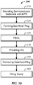
- FIG. 10 An exemplary flow chart according to embodiments of the present invention is shown in FIG. 10 and is used as illustration only.
- FIG. 2 shows a schematic drawing of an intermediate product, obtained by forming a sacrificial plug (also referred to as a buried plug) 120 on the liner 130, after BPR metal recess and after liner 130 deposition, in accordance with embodiments of the present invention.
- a sacrificial plug also referred to as a buried plug
- devices 140 are shown which may be formed by FEOL processing.
- FIG. 3 shows a schematic drawing of an intermediate product, obtained after VBPR etch landing on the buried plug 120, in accordance with embodiments of the present invention.
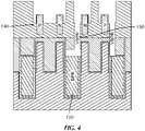
- FIG. 4 shows a schematic drawing of an intermediate product, obtained after removal of the buried plug, in accordance with embodiments of the present invention.
- the buried plug 120, or the buried plug 120 and the liner 130 on top of the BPR may be removed.
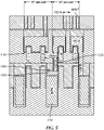
- FIG. 5 shows a schematic drawing of an intermediate product, obtained after replacing the sacrificial buried plug with a metal 160, in accordance with embodiments of the present invention.
- two Vias are shown.
- the left Via 150 is in contact with the BPR through the metal which is replacing the buried plug.
- a larger contact area is obtained than for the right Via which is a conventional Via in direct contact with the BPR.
- the VBPR and BPR contact surface can be enlarged to full BPR CD after replacing the plug with VBPR metal.
- the sacrificial plug 120 may be removed 250 by wet or isotropic selective etching.
- amorphous silicon is used for forming 220 the sacrificial plug 120.
- amorphous carbon is used for forming 220 the sacrificial plug 120.
- the sacrificial plug is formed on top of the BPR at the position of the Via BPR landing area.
- the step of forming 220 the sacrificial plug 120 at a contact surface 130 on the buried power rail 110 may be followed by an oxide fill step and a shallow trench isolation (STI) chemical-mechanical polishing step, followed by a conventional FEOL module.
- STI shallow trench isolation
- a VBPR landing is achieved on the amorphous plug.
- the contact surface 130 may be the surface of the BPR itself.
- the contact surface 130 may be a liner.
- the sacrificial plug 120 is formed 220 after recess of the buried power rail metal and after deposition of a liner 130 on the buried power rail and wherein the liner 130 is removed after removing 250 the sacrificial plug and before filling 260 the cavity with the metal.
- a liner 131 may be deposited after forming 220 the sacrificial plug.
- the liner 130, 131 on the buried power rail or on the sacrificial plug also referred as the BPR liner, can protect the BPR metal surface from oxidation during STI oxide annealing.
- the BPR liner 130 may be removed by wet or isotropic selective etching.
- the VBPR is connected to the BPR. It is an advantage of embodiments of the present invention that the contact surface with the BPR can be greatly enlarged compared to a conventional Via.
- filling the cavity with a metal may be achieved by atomic layer deposition (ALD) or metal on metal selective deposition for full filling the cavity formed after removal of the plug. Also the remaining part may be filled by ALD or metal on metal selective deposition.
- ALD atomic layer deposition
- metal on metal selective deposition for full filling the cavity formed after removal of the plug. Also the remaining part may be filled by ALD or metal on metal selective deposition.
- the remaining part may be filled by conventional chemical vapor deposition (CVD).
- CVD chemical vapor deposition
- the metal may for example be W, Co, Ru, Mo, or combinations of these metals.
- the invention is, however, not limited thereto.
- Area selective deposition may be more attractive for filling the cavity because it is bottom up and barrier less. Area selective deposition allows selective deposition, metal on metal, and bottom up filling of the cavity.
- a barrier layer 180 is formed by ALD deposition. Indeed, In the ALD case, a thin barrier layer must be deposited before the metal deposition.
- An ALD barrier like Ti/TiN/TaN may be used for ALD W/Co/Ru deposition.
- FIG. 5 shows a stack obtained after applying metal lines (M0A), for example in a middle end of line layer, and metal interconnects (MINT), for example in a back end of line layer.
- M0A metal lines
- MINT metal interconnects
- FIG. 5 shows a stack obtained after applying metal lines (M0A), for example in a middle end of line layer, and metal interconnects (MINT), for example in a back end of line layer.
- MINT metal interconnects
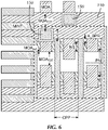
- FIG. 6 shows a top view of a semiconductor device which is obtained after conventional via landing.
- FIG. 6 shows a 5-track std cell (90 nm) with metal interconnect pitch of 18 nm.
- the contacted poly pitch CPP is 42 nm.
- the metal interconnect (MINT) corresponds with the 1 st metal layer (horizontal).
- the hashed square 190 shows the available space for a VBPR 150 in a standard cell.
- the bottom CD of the contact between the Via 150 and the BPR 110 is smaller than the top CD.
- the available space for VBPR in a std. cell is 12-18 nm, for a CPP of 42 nm and a gate length of 14 nm.
- FIGs. 7 and 8 show top views of semiconductor devices which are obtained using a method in accordance with embodiments of the present invention.
- the VBPR bottom contact 160 (i.e. the cavity filled with metal) has a length which is extended to the full BPR 110 width. For example from 12-18 nm to 24-48 nm.
- the vias 150 land on the VBPR bottom contact 160.
- a bottom contact CD can be obtained which is significantly larger than a top CD.
- the Y CD (this is the dimension orthogonal to the BPR and parallel with the substrate, please) can self align to the BPR. The reason therefore is that the VBPR Y bottom CD is the same as the BPR metal top CD.
- the vias 150 land on the VBPR bottom contact 160.
- the VBPR bottom contact 160 has an extended bottom contact compared to the contact width of a state of the art Via. As illustrated in FIG. 8 the VBPR bottom contact width may even be extended beyond the contacted poly pitch CPP. For example from 12-18 nm to 30-50 nm. In this example the illustration is for nanosheet NS.
- the plug area may for example be defined by the lithography print.
- the range can for example be the same as the M0A CD.
- two neighboring VBPR may share the same via bottom contact, which allows to extend the via bottom contact even more (e.g. to over 50 nm).
- FIG. 9 shows a top view of a semiconductor device, for which the via bottom contact 160 is shared between two vias 150, and which is obtained using a method in accordance with embodiments of the present invention.
- the via bottom contact 160 is buried under the gate 165.
- the VBPR may be self-aligned to the gate.
- the plug height may be limited by the BPR CD. In embodiments of the present invention the plug may for example a height between 12 and 24 nm or 12 to 48 nm, depending on the BPR CD in design. It may for example have a height of 20 nm.
- the VBPR metal can for example be made of W or Co or Mo, or Ru or combination of these metals.
- the RMG Gate can for example be made of TiN or TaN or W or TiAIC.
- the M0A can for example be made of W, Co, Mo, Ru.
- the BPR can for example be made of W,Co, Mo, Ru.
- the inventors have found a process flow which allows to decrease the resistivity of the contact of the Via with the BPR.
- This process flow can be integrated in standard process flows which may for example comprise well implant, fin forming and STI, forming buried power rails, fin reveal, gate and spacer formation, source and drain epitaxial growth, activation anneal, ILD0, replacement metal gate, M0A, M0G, MIV0 as steps in the FEOL.
- the buried plug is formed before the contact hole (i.e. the Via).
- the sacrificial plug may be formed by lithography.
- self-aligned contacts can be obtained. This is essential for technologies with small CD (e.g. 3 nm node).
- the buried plug is formed before the Via, self-aligned contacts can be obtained, and the Via etching aspect ratio can be reduced compared to methods where this self-alignment is not possible.
- Buried power rails may for example be used to interconnect standard cells and/or to distribute power to the standard cells.
- a plug liner may be deposited first, and a BPR liner last. This is illustrated in FIG. 10 and FIG. 11 .
- a BPR liner may be deposited first followed by the deposition of a plug liner. This is illustrated in FIG. 12 .
- FIG. 10 shows cross-sections of intermediate products obtained using a method in accordance with embodiments of the present invention.
- the top cross-sections are made orthogonal with the BPR 110.
- the bottom cross-section is made along the BPR (i.e. in the length direction of the BPR and orthogonal to the substrate 105.
- the substrate 105 is a Silicon substrate.
- the top left cross-section shows a BPR 110 obtained after BPR metal recess.
- the BPR 110 comprises a metal in a trench of the substrate 105.
- the walls of the trench are covered by oxide 107.
- the figures also shows STI oxides 107. Between the STI oxides and the trench, fins 106 are shown.
- the second drawing from the left shows an intermediate product obtained after depositing a plug liner PL (e.g. oxide) and after depositing plug material 120 (e.g. aSi or APF).
- a plug liner PL e.g. oxide
- plug material 120 e.g. aSi or APF
- the plug liner PL may be skipped, depending on the plug material and the BPR metal type.
- a BPR liner (e.g. SiO2) instead of a plug liner may be deposited.
- the BPR liner deposition step may be followed by a plug material deposition step. (e.G. aSi or APF). It is noted that in case of using a SiN BPR liner, it may be more difficult to remove it after sacrificial plug removal. No mask is required.
- the third top drawing from the left shows a schematic drawing of an intermediate stack obtained after chemical mechanical polishing (CMP) of the plug and after etching back of the plug 120.
- CMP chemical mechanical polishing
- the corresponding drawing at the bottom of the figure shows a cross-section of the same intermediate stack, cut along the BPR.
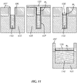
- FIG. 11 show cross-sections of intermediate stacks, orthogonal to the BPR and the bottom drawings show the corresponding cross-sections along the BPR, wherein the intermediate stacks are obtained using a method in accordance with embodiments of the present invention.
- the first drawings from the left show the intermediate stacks obtained after patterning of the sacrificial plug 120. This may be achieved by lithography/etch patterning and can be self-aligned to the BPR width (e.g. through block print, defining the sacrificial plug size, and landing on BPR).
- the middle drawings show an intermediate stack obtained after a BPR liner (BPRL) deposition, in accordance with embodiments of the present invention.
- the BPR liner may for example be a SiN liner.
- FIG. 5 The right drawings show an intermediate stack obtained after STI oxide fill 108 and CMP, in accordance with embodiments of the present invention. Starting from such a stack, a stack as in FIG. 5 can be obtained, by applying method steps in accordance with embodiments of the present invention.
- FIG. 12 show intermediate stack in case a BPR liner BPRL is deposited before the deposition of a plug liner PL.
- the top cross-sections are made orthogonal with the BPR 110.
- the bottom cross-section are made along the BPR (i.e. in the length direction of the BPR and orthogonal to the substrate.
- the first drawings from the left show the intermediate stacks obtained after patterning of the sacrificial plug. This may be achieved by lithography/etch patterning and can be self-aligned to the BPR width (e.g. through block print, defining the sacrificial plug size, and landing on the BPR liner).
- the second drawings from the left show the intermediate stack obtained after plug liner PL deposition in accordance with embodiments of the present invention.
- the plug liner may for example be a SiN liner, or a SiO liner.
- a plug liner is, however, not strictly required.
- the right drawings show an intermediate stack obtained after STI oxide fill and CMP, in accordance with embodiments of the present invention.
Landscapes
- Internal Circuitry In Semiconductor Integrated Circuit Devices (AREA)
Abstract
Description
- The present invention relates to buried power rails. More specifically it relates to the formation of a contact with a buried power rail.
- Power rails, used for delivering power to the transistors of a chip, are typically implemented in the back-end-of-line.
- In order to create more routing possibilities for the interconnects, buried power rails (BPR) may be applied before the front-end-of-line module.
- Creating electrical contacts with these buried power rails is, however, very challenging in view of the resistivity of these contacts, especially with decreasing critical dimensions.
- For example the Via connect VBPR (Via connection with BPR) between a metallization layer M0 and the BPR may be scaled to 10-15 nm bottom CD in iN3 and beyond. This creates a major concern of its resistivity and its impact on the device performance.
-
FIG. 1 shows a schematic drawing of a vertical cross-section of a semiconductor product stack illustrating aBPR 110 in iN3. In this figure a via (VBPR) is connected with a BPR. It can be seen that a decreasing CD will result in a decreasing contact surface between the VBPR and the BPR. This may even result in a width of the VBPR reducing to less than 12 nm. In the figure neighboring 5T std cells with a width of 90 nm are shown. At the top side of the drawing metal interconnects are shown. The sum of the width of a metal interconnect and distance between two metal interconnects is in this example equal to 18 nm. In the example the BPR is formed in aSi substrate 105. Anoxide 107 is present between the BPR and thesubstrate 105. - In view of this reduced resistivity with decreasing critical dimensions, there is a need to provide a method which allows to provide a good electrical connection between a buried power layer and a Via.
- It is an object the present invention to provide a good method for electrically contacting a BPR.
- The above objective is accomplished by a method and device according to the present invention.
- Embodiments of the present invention relate to a method for forming a semiconductor product comprising a buried contact with a buried power rail.
The method comprises the following steps: - providing a semiconductor substrate comprising a buried power rail,
- forming a sacrificial plug at a contact surface on the buried power rail,
- applying a front-end-of-line module for forming devices in the semiconductor substrate,
- providing a Via, through layers applied by the front-end-module, which joins the sacrificial plug on the buried power rail,
- selectively removing the sacrificial plug thereby obtaining a cavity above the buried power rail,
- filling the cavity with a metal to electrically connect the devices with the buried power rail, wherein the sacrificial plug is formed such that the contact surface area is larger than an area of a cross-section of the Via parallel with the contact surface.
- It is an advantage of embodiments of the present invention the resistivity of the connection between the Via and the BPR is reduced by providing a sacrificial plug at the contact surface before applying the front-end-module, and by replacing the sacrificial plug with a metal.
- It is an advantage of embodiments of the present invention the Via to BPR contact surface area can be enlarged and that it is not limited by the bottom critical dimension of the Via.
- Particular and preferred aspects of the invention are set out in the accompanying independent and dependent claims. Features from the dependent claims may be combined with features of the independent claims and with features of other dependent claims as appropriate and not merely as explicitly set out in the claims.
- These and other aspects of the invention will be apparent from and elucidated with reference to the embodiment(s) described hereinafter.
-
-
FIG. 1 shows a schematic drawing of a vertical cross-section of a semiconductor product stack illustrating a buried power rail. -
FIG. 2 shows a schematic drawing of an intermediate product, obtained by forming a sacrificial plug on a buried power rail, in accordance with embodiments of the present invention. -
FIG. 3 shows a schematic drawing of an intermediate product, obtained after via etch landing on the buried plug, in accordance with embodiments of the present invention. -
FIG. 4 shows a schematic drawing of an intermediate product, obtained after removal of the buried plug, in accordance with embodiments of the present invention. -
FIG. 5 shows a schematic drawing of an intermediate product, obtained after replacing the sacrificial buried plug with a metal, in accordance with embodiments of the present invention. -
FIG. 6 shows a top view of a semiconductor device which is obtained after conventional via landing. -
FIG. 7 shows a top view of a semiconductor device, for which the via bottom contact has a length which is extended to the full width of the buried power rail, and which is obtained using a method in accordance with embodiments of the present invention. -
FIG. 8 shows a top view of a semiconductor device, for which the via bottom contact has an extended width compared to the width of the via inFIG. 6 , and which is obtained using a method in accordance with embodiments of the present invention. -
FIG. 9 shows a top view of a semiconductor device, for which the via bottom contact is shared between two vias, and which is obtained using a method in accordance with embodiments of the present invention. -
FIG. 10 shows a flow chart of an exemplary method in accordance with embodiments of the present invention. -
FIG. 11 shows cross-sections of intermediate products obtained using a method in accordance with embodiments of the present invention. -
FIG. 12 shows cross-sections of intermediate products obtained using a method in accordance with embodiments of the present invention, wherein a plug liner is deposited before a buried power rail liner. -
FIG. 13 shows cross-sections of intermediate products obtained using a method in accordance with embodiments of the present invention, wherein a buried power rail liner is deposited before a plug liner. - Any reference signs in the claims shall not be construed as limiting the scope. In the different drawings, the same reference signs refer to the same or analogous elements.
- The present invention will be described with respect to particular embodiments and with reference to certain drawings but the invention is not limited thereto but only by the claims. The drawings described are only schematic and are non-limiting. In the drawings, the size of some of the elements may be exaggerated and not drawn on scale for illustrative purposes. The dimensions and the relative dimensions do not correspond to actual reductions to practice of the invention.
- Moreover, the terms top, under and the like in the description and the claims are used for descriptive purposes and not necessarily for describing relative positions. It is to be understood that the terms so used are interchangeable under appropriate circumstances and that the embodiments of the invention described herein are capable of operation in other orientations than described or illustrated herein.
- It is to be noticed that the term "comprising", used in the claims, should not be interpreted as being restricted to the means listed thereafter; it does not exclude other elements or steps. It is thus to be interpreted as specifying the presence of the stated features, integers, steps or components as referred to, but does not preclude the presence or addition of one or more other features, integers, steps or components, or groups thereof. Thus, the scope of the expression "a device comprising means A and B" should not be limited to devices consisting only of components A and B. It means that with respect to the present invention, the only relevant components of the device are A and B.
- Reference throughout this specification to "one embodiment" or "an embodiment" means that a particular feature, structure or characteristic described in connection with the embodiment is included in at least one embodiment of the present invention. Thus, appearances of the phrases "in one embodiment" or "in an embodiment" in various places throughout this specification are not necessarily all referring to the same embodiment, but may. Furthermore, the particular features, structures or characteristics may be combined in any suitable manner, as would be apparent to one of ordinary skill in the art from this disclosure, in one or more embodiments.
- Similarly it should be appreciated that in the description of exemplary embodiments of the invention, various features of the invention are sometimes grouped together in a single embodiment, figure, or description thereof for the purpose of streamlining the disclosure and aiding in the understanding of one or more of the various inventive aspects. This method of disclosure, however, is not to be interpreted as reflecting an intention that the claimed invention requires more features than are expressly recited in each claim. Rather, as the following claims reflect, inventive aspects lie in less than all features of a single foregoing disclosed embodiment. Thus, the claims following the detailed description are hereby expressly incorporated into this detailed description, with each claim standing on its own as a separate embodiment of this invention.
- Furthermore, while some embodiments described herein include some but not other features included in other embodiments, combinations of features of different embodiments are meant to be within the scope of the invention, and form different embodiments, as would be understood by those in the art. For example, in the following claims, any of the claimed embodiments can be used in any combination.
- In the description provided herein, numerous specific details are set forth. However, it is understood that embodiments of the invention may be practiced without these specific details. In other instances, well-known methods, structures and techniques have not been shown in detail in order not to obscure an understanding of this description.
- Embodiments of the present invention relate to a method for forming a semiconductor product comprising a buried contact with a buried power rail.
- An exemplary flow chart according to embodiments of the present invention is shown in
FIG. 10 and is used as illustration only. - A method in accordance with embodiments of the present invention comprises at least the following steps:
- providing 210 a semiconductor substrate comprising a buried
power rail 110, - forming 220 a
sacrificial plug 120 at acontact surface 130 on the buriedpower rail 110, - applying 230 a front-end-of-line module for forming
devices 140 in the semiconductor substrate, - providing 240 a
Via 150, through layers applied by the front-end-module, which joins thesacrificial plug 120 on the buriedpower rail 110, - selectively removing 250 the
sacrificial plug 120 thereby obtaining a cavity above the buried power rail, - filling 260 the cavity with a
metal 160 to electrically connect thedevices 140 with the buriedpower rail 110, wherein thesacrificial plug 120 is formed such that the contact surface area is larger than an area of a cross-section of theVia 150 parallel with the contact surface. -
FIG. 2 shows a schematic drawing of an intermediate product, obtained by forming a sacrificial plug (also referred to as a buried plug) 120 on theliner 130, after BPR metal recess and afterliner 130 deposition, in accordance with embodiments of the present invention. In this drawing alsodevices 140 are shown which may be formed by FEOL processing. -
FIG. 3 shows a schematic drawing of an intermediate product, obtained after VBPR etch landing on the buriedplug 120, in accordance with embodiments of the present invention. -
FIG. 4 shows a schematic drawing of an intermediate product, obtained after removal of the buried plug, in accordance with embodiments of the present invention. In embodiments of the present invention only the buriedplug 120, or the buriedplug 120 and theliner 130 on top of the BPR may be removed. - In embodiments of the present invention the obtained cavity may be filled with a metal.
FIG. 5 shows a schematic drawing of an intermediate product, obtained after replacing the sacrificial buried plug with ametal 160, in accordance with embodiments of the present invention. In this figure two Vias are shown. Theleft Via 150 is in contact with the BPR through the metal which is replacing the buried plug. Thus, a larger contact area is obtained than for the right Via which is a conventional Via in direct contact with the BPR. It is an advantage of embodiments of the present invention that the VBPR and BPR contact surface can be enlarged to full BPR CD after replacing the plug with VBPR metal. - In embodiments of the present invention the
sacrificial plug 120 may be removed 250 by wet or isotropic selective etching. - In embodiments of the present invention amorphous silicon is used for forming 220 the
sacrificial plug 120. - In embodiments of the present invention amorphous carbon (APF) is used for forming 220 the
sacrificial plug 120. - In embodiments of the present invention the sacrificial plug is formed on top of the BPR at the position of the Via BPR landing area.
- The step of forming 220 the
sacrificial plug 120 at acontact surface 130 on the buriedpower rail 110 may be followed by an oxide fill step and a shallow trench isolation (STI) chemical-mechanical polishing step, followed by a conventional FEOL module. - Next, in embodiments of the present invention, a VBPR landing is achieved on the amorphous plug.
- In embodiments of the present invention the
contact surface 130 may be the surface of the BPR itself. - In embodiments of the present invention the
contact surface 130 may be a liner. - In embodiments of the present invention the
sacrificial plug 120 is formed 220 after recess of the buried power rail metal and after deposition of aliner 130 on the buried power rail and wherein theliner 130 is removed after removing 250 the sacrificial plug and before filling 260 the cavity with the metal. - In embodiments of the present invention a liner 131 may be deposited after forming 220 the sacrificial plug.
- The
liner 130, 131 on the buried power rail or on the sacrificial plug , also referred as the BPR liner, can protect the BPR metal surface from oxidation during STI oxide annealing. - The
BPR liner 130 may be removed by wet or isotropic selective etching. - By filling the cavity the VBPR is connected to the BPR. It is an advantage of embodiments of the present invention that the contact surface with the BPR can be greatly enlarged compared to a conventional Via.
- In embodiments of the present invention filling the cavity with a metal may be achieved by atomic layer deposition (ALD) or metal on metal selective deposition for full filling the cavity formed after removal of the plug. Also the remaining part may be filled by ALD or metal on metal selective deposition.
- Alternatively, the remaining part may be filled by conventional chemical vapor deposition (CVD).
- The metal may for example be W, Co, Ru, Mo, or combinations of these metals. The invention is, however, not limited thereto.
- Area selective deposition may be more attractive for filling the cavity because it is bottom up and barrier less. Area selective deposition allows selective deposition, metal on metal, and bottom up filling of the cavity.
- In the example of
FIG. 5 , on the contrary, abarrier layer 180 is formed by ALD deposition. Indeed, In the ALD case, a thin barrier layer must be deposited before the metal deposition. An ALD barrier like Ti/TiN/TaN may be used for ALD W/Co/Ru deposition. - In metal on metal selective deposition, such as W or Ru, deposition of the barrier can be skipped, which can significantly reduce the metal/metal contact resistivity.
FIG. 5 shows a stack obtained after applying metal lines (M0A), for example in a middle end of line layer, and metal interconnects (MINT), for example in a back end of line layer. In the example the vias interconnect the metal lines (M0A) with the BPR. -
FIG. 6 shows a top view of a semiconductor device which is obtained after conventional via landing.FIG. 6 shows a 5-track std cell (90 nm) with metal interconnect pitch of 18 nm. In this example the contacted poly pitch CPP is 42 nm. The metal interconnect (MINT) corresponds with the 1st metal layer (horizontal). The hashed square 190 shows the available space for a VBPR 150 in a standard cell. As can be seen from this figure the bottom CD of the contact between theVia 150 and theBPR 110 is smaller than the top CD. In this example the available space for VBPR in a std. cell is 12-18 nm, for a CPP of 42 nm and a gate length of 14 nm. -
FIGs. 7 and8 show top views of semiconductor devices which are obtained using a method in accordance with embodiments of the present invention. - In
FIG. 7 the VBPR bottom contact 160 (i.e. the cavity filled with metal) has a length which is extended to thefull BPR 110 width. For example from 12-18 nm to 24-48 nm. Thevias 150 land on theVBPR bottom contact 160. As can be seen from this figure a bottom contact CD can be obtained which is significantly larger than a top CD. It is, moreover, advantageous that the Y CD (this is the dimension orthogonal to the BPR and parallel with the substrate, please) can self align to the BPR. The reason therefore is that the VBPR Y bottom CD is the same as the BPR metal top CD. - Also in
FIG. 8 thevias 150 land on theVBPR bottom contact 160. TheVBPR bottom contact 160 has an extended bottom contact compared to the contact width of a state of the art Via. As illustrated inFIG. 8 the VBPR bottom contact width may even be extended beyond the contacted poly pitch CPP. For example from 12-18 nm to 30-50 nm. In this example the illustration is for nanosheet NS. - The plug area may for example be defined by the lithography print. The range can for example be the same as the M0A CD.
- In embodiments of the present invention two neighboring VBPR may share the same via bottom contact, which allows to extend the via bottom contact even more (e.g. to over 50 nm).
FIG. 9 shows a top view of a semiconductor device, for which the viabottom contact 160 is shared between twovias 150, and which is obtained using a method in accordance with embodiments of the present invention. In embodiments of the present invention the viabottom contact 160 is buried under thegate 165. In embodiments of the present invention the VBPR may be self-aligned to the gate. - In embodiments of the present invention the plug height may be limited by the BPR CD. In embodiments of the present invention the plug may for example a height between 12 and 24 nm or 12 to 48 nm, depending on the BPR CD in design. It may for example have a height of 20 nm.
- In embodiments of the present invention the VBPR metal can for example be made of W or Co or Mo, or Ru or combination of these metals. The RMG Gate can for example be made of TiN or TaN or W or TiAIC. The M0A can for example be made of W, Co, Mo, Ru. The BPR can for example be made of W,Co, Mo, Ru.
- The inventors have found a process flow which allows to decrease the resistivity of the contact of the Via with the BPR. This process flow can be integrated in standard process flows which may for example comprise well implant, fin forming and STI, forming buried power rails, fin reveal, gate and spacer formation, source and drain epitaxial growth, activation anneal, ILD0, replacement metal gate, M0A, M0G, MIV0 as steps in the FEOL.
- It is an advantage of a method, in accordance with embodiments of the present invention, that the buried plug is formed before the contact hole (i.e. the Via). In embodiments of the present invention the sacrificial plug may be formed by lithography. By the use of a method in accordance with embodiments of the present invention, self-aligned contacts can be obtained. This is essential for technologies with small CD (e.g. 3 nm node). As the buried plug is formed before the Via, self-aligned contacts can be obtained, and the Via etching aspect ratio can be reduced compared to methods where this self-alignment is not possible.
- Buried power rails may for example be used to interconnect standard cells and/or to distribute power to the standard cells.
- In embodiments of the present invention a plug liner may be deposited first, and a BPR liner last. This is illustrated in
FIG. 10 andFIG. 11 . - Alternatively, in embodiments of the present invention a BPR liner may be deposited first followed by the deposition of a plug liner. This is illustrated in
FIG. 12 . - The top schematic drawings in
FIG. 10 shows cross-sections of intermediate products obtained using a method in accordance with embodiments of the present invention. The top cross-sections are made orthogonal with theBPR 110. The bottom cross-section is made along the BPR (i.e. in the length direction of the BPR and orthogonal to thesubstrate 105. - In the examples the
substrate 105 is a Silicon substrate. The top left cross-section shows aBPR 110 obtained after BPR metal recess. TheBPR 110 comprises a metal in a trench of thesubstrate 105. The walls of the trench are covered byoxide 107. The figures also showsSTI oxides 107. Between the STI oxides and the trench,fins 106 are shown. - The second drawing from the left shows an intermediate product obtained after depositing a plug liner PL (e.g. oxide) and after depositing plug material 120 (e.g. aSi or APF). In embodiments of the present invention the plug liner PL may be skipped, depending on the plug material and the BPR metal type.
- In embodiments of the present invention, at this stage of the process, a BPR liner (e.g. SiO2) instead of a plug liner may be deposited. The BPR liner deposition step may be followed by a plug material deposition step. (e.G. aSi or APF). It is noted that in case of using a SiN BPR liner, it may be more difficult to remove it after sacrificial plug removal. No mask is required.
- The third top drawing from the left shows a schematic drawing of an intermediate stack obtained after chemical mechanical polishing (CMP) of the plug and after etching back of the
plug 120. The corresponding drawing at the bottom of the figure shows a cross-section of the same intermediate stack, cut along the BPR. - Similarly as in
FIG. 10 , the top drawings inFIG. 11 show cross-sections of intermediate stacks, orthogonal to the BPR and the bottom drawings show the corresponding cross-sections along the BPR, wherein the intermediate stacks are obtained using a method in accordance with embodiments of the present invention. - The first drawings from the left show the intermediate stacks obtained after patterning of the
sacrificial plug 120. This may be achieved by lithography/etch patterning and can be self-aligned to the BPR width (e.g. through block print, defining the sacrificial plug size, and landing on BPR). - The middle drawings show an intermediate stack obtained after a BPR liner (BPRL) deposition, in accordance with embodiments of the present invention. The BPR liner may for example be a SiN liner.
- The right drawings show an intermediate stack obtained after STI oxide fill 108 and CMP, in accordance with embodiments of the present invention. Starting from such a stack, a stack as in
FIG. 5 can be obtained, by applying method steps in accordance with embodiments of the present invention. - The drawings in
FIG. 12 show intermediate stack in case a BPR liner BPRL is deposited before the deposition of a plug liner PL. The top cross-sections are made orthogonal with theBPR 110. The bottom cross-section are made along the BPR (i.e. in the length direction of the BPR and orthogonal to the substrate. The first drawings from the left show the intermediate stacks obtained after patterning of the sacrificial plug. This may be achieved by lithography/etch patterning and can be self-aligned to the BPR width (e.g. through block print, defining the sacrificial plug size, and landing on the BPR liner). - The second drawings from the left show the intermediate stack obtained after plug liner PL deposition in accordance with embodiments of the present invention. The plug liner may for example be a SiN liner, or a SiO liner. A plug liner is, however, not strictly required.
The right drawings show an intermediate stack obtained after STI oxide fill and CMP, in accordance with embodiments of the present invention.
Claims (8)
- A method (200) for forming a semiconductor product comprising a buried contact with a buried power rail, the method comprising:- providing (210) a semiconductor substrate comprising a buried power rail (110),- forming (220) a sacrificial plug (120) at a contact surface (130) on the buried power rail (110),- applying (230) a front-end-of-line module for forming devices (140) in the semiconductor substrate,- providing (240) a Via (150), through layers applied by the front-end-module, which joins the sacrificial plug (120) on the buried power rail (110),- selectively removing (250) the sacrificial plug (120) thereby obtaining a cavity above the buried power rail,- filling (260) the cavity with a metal (160) to electrically connect the devices (140) with the buried power rail (110), wherein the sacrificial plug (120) is formed such that the contact surface area is larger than an area of a cross-section of the Via (150) parallel with the contact surface.
- A method (200) according to claim 1, wherein the sacrificial plug (120) is removed (250) by wet or isotropic selective etching.
- A method (200) according to any of the previous claims wherein amorphous silicon is used for forming (220) the sacrificial plug (120).
- A method (200) according to any of the claims 1 or 2 wherein amorphous carbon is used for forming (220) the sacrificial plug (120).
- A method (200) according to any of the previous claims wherein the sacrificial plug (120) is formed (220) after recess of the buried power rail metal and after deposition of a liner (130) on the buried power rail and wherein the liner (130) is removed after removing (250) the sacrificial plug and before filling (260) the cavity with the metal.
- A method (200) according to any of the claims 1 to 4 wherein a liner (131) is deposited after forming (220) the sacrificial plug (120).
- A method (200) according to any of the previous claims wherein filling the cavity with the metal (160) is done using area selective deposition.
- A method (200) according to any of the claims 1 to 6 wherein filling the cavity with the metal (160) is done using metal on metal selective deposition.
Priority Applications (3)
| Application Number | Priority Date | Filing Date | Title |
|---|---|---|---|
| EP20211727.1A EP4009360B1 (en) | 2020-12-03 | 2020-12-03 | Buried power rail contact formation |
| CN202110718250.9A CN114597160A (en) | 2020-12-03 | 2021-06-28 | Buried Power Rail Contact Formation |
| US17/459,384 US11776841B2 (en) | 2020-12-03 | 2021-08-27 | Buried power rail contact formation |
Applications Claiming Priority (1)
| Application Number | Priority Date | Filing Date | Title |
|---|---|---|---|
| EP20211727.1A EP4009360B1 (en) | 2020-12-03 | 2020-12-03 | Buried power rail contact formation |
Publications (2)
| Publication Number | Publication Date |
|---|---|
| EP4009360A1 true EP4009360A1 (en) | 2022-06-08 |
| EP4009360B1 EP4009360B1 (en) | 2023-05-03 |
Family
ID=73726562
Family Applications (1)
| Application Number | Title | Priority Date | Filing Date |
|---|---|---|---|
| EP20211727.1A Active EP4009360B1 (en) | 2020-12-03 | 2020-12-03 | Buried power rail contact formation |
Country Status (3)
| Country | Link |
|---|---|
| US (1) | US11776841B2 (en) |
| EP (1) | EP4009360B1 (en) |
| CN (1) | CN114597160A (en) |
Cited By (1)
| Publication number | Priority date | Publication date | Assignee | Title |
|---|---|---|---|---|
| US20240315051A1 (en) * | 2020-06-29 | 2024-09-19 | Taiwan Semiconductor Manufacturing Co., Ltd. | Semiconductor device and method for forming the same |
Families Citing this family (6)
| Publication number | Priority date | Publication date | Assignee | Title |
|---|---|---|---|---|
| US20230154784A1 (en) * | 2021-11-17 | 2023-05-18 | International Business Machines Corporation | Bottom dielectric isolation integration with buried power rail |
| US12463136B2 (en) * | 2022-04-29 | 2025-11-04 | Samsung Electronics Co., Ltd. | Integrated circuit devices including backside power rail and methods of forming the same |
| US12424539B2 (en) * | 2022-09-06 | 2025-09-23 | International Business Machines Corporation | Local enlarged via-to-backside power rail |
| US12484248B2 (en) | 2022-10-25 | 2025-11-25 | International Business Machines Corporation | Source/drain contact at tight cell boundary |
| US12457780B2 (en) | 2022-12-01 | 2025-10-28 | International Business Machines Corporation | Semiconductor device with void under source/drain region for backside contact |
| US12501698B2 (en) | 2022-12-22 | 2025-12-16 | International Business Machines Corporation | Stacked transistors having self aligned backside contact with backside replacement metal gate |
Citations (3)
| Publication number | Priority date | Publication date | Assignee | Title |
|---|---|---|---|---|
| US20050212018A1 (en) * | 2003-07-30 | 2005-09-29 | Stmicroelectronics S.A. | Conductive lines buried in insulating areas |
| US20180374791A1 (en) * | 2017-06-22 | 2018-12-27 | Tokyo Electron Limited | Buried power rails |
| US20200135578A1 (en) * | 2018-10-31 | 2020-04-30 | Taiwan Semiconductor Manufacturing Co., Ltd. | Integrated Circuits with Buried Interconnect Conductors |
Family Cites Families (8)
| Publication number | Priority date | Publication date | Assignee | Title |
|---|---|---|---|---|
| US7511349B2 (en) | 2005-08-19 | 2009-03-31 | Taiwan Semiconductor Manufacturing Company, Ltd. | Contact or via hole structure with enlarged bottom critical dimension |
| KR20100022348A (en) | 2008-08-19 | 2010-03-02 | 주식회사 하이닉스반도체 | Method for forming semiconductor device |
| KR101602451B1 (en) | 2010-01-22 | 2016-03-16 | 삼성전자주식회사 | Method of forming semiconductor device having contact plug and related device |
| KR102001493B1 (en) * | 2013-04-16 | 2019-07-18 | 에스케이하이닉스 주식회사 | Semiconductor device with air gap and method for fabricating the same |
| US10861745B2 (en) * | 2017-11-30 | 2020-12-08 | Taiwan Semiconductor Manufacturing Company, Ltd. | Semiconductor device and method of manufacture |
| CN110896075B (en) * | 2018-09-13 | 2022-02-08 | 长鑫存储技术有限公司 | Integrated circuit memory and method of making the same |
| US10720391B1 (en) | 2019-01-04 | 2020-07-21 | Globalfoundries Inc. | Method of forming a buried interconnect and the resulting devices |
| US11101217B2 (en) * | 2019-06-27 | 2021-08-24 | International Business Machines Corporation | Buried power rail for transistor devices |
-
2020
- 2020-12-03 EP EP20211727.1A patent/EP4009360B1/en active Active
-
2021
- 2021-06-28 CN CN202110718250.9A patent/CN114597160A/en active Pending
- 2021-08-27 US US17/459,384 patent/US11776841B2/en active Active
Patent Citations (3)
| Publication number | Priority date | Publication date | Assignee | Title |
|---|---|---|---|---|
| US20050212018A1 (en) * | 2003-07-30 | 2005-09-29 | Stmicroelectronics S.A. | Conductive lines buried in insulating areas |
| US20180374791A1 (en) * | 2017-06-22 | 2018-12-27 | Tokyo Electron Limited | Buried power rails |
| US20200135578A1 (en) * | 2018-10-31 | 2020-04-30 | Taiwan Semiconductor Manufacturing Co., Ltd. | Integrated Circuits with Buried Interconnect Conductors |
Cited By (2)
| Publication number | Priority date | Publication date | Assignee | Title |
|---|---|---|---|---|
| US20240315051A1 (en) * | 2020-06-29 | 2024-09-19 | Taiwan Semiconductor Manufacturing Co., Ltd. | Semiconductor device and method for forming the same |
| US12317513B2 (en) * | 2020-06-29 | 2025-05-27 | Taiwan Semiconductor Manufacturing Company, Ltd. | Semiconductor device and method for forming the same |
Also Published As
| Publication number | Publication date |
|---|---|
| CN114597160A (en) | 2022-06-07 |
| US11776841B2 (en) | 2023-10-03 |
| EP4009360B1 (en) | 2023-05-03 |
| US20220181197A1 (en) | 2022-06-09 |
Similar Documents
| Publication | Publication Date | Title |
|---|---|---|
| EP4009360B1 (en) | Buried power rail contact formation | |
| US12376356B2 (en) | Semiconductor devices with backside power rail and methods of fabrication thereof | |
| US12211787B2 (en) | Interconnect structures and methods of fabrication thereof | |
| US11721590B2 (en) | Semiconductor device and method | |
| KR102716576B1 (en) | Multigate device with air gap spacer and backside rail contact and method of fabricating thereof | |
| CN105977284A (en) | Source/drain regions for fin field effect transistors and methods of forming same | |
| KR102568602B1 (en) | Semiconductor device and method | |
| CN106098557A (en) | Semiconductor structure and forming method thereof | |
| US12094973B2 (en) | Semiconductor devices with backside power rail and methods of fabrication thereof | |
| US20250221025A1 (en) | Stacked device structures and methods for forming the same | |
| US20240290864A1 (en) | Backside gate contact, backside gate etch stop layer, and methods of forming same | |
| KR20210134205A (en) | Nterconnect structure and method | |
| CN119318217A (en) | Self-aligned backside contacts with increased contact area | |
| CN114664735B (en) | Methods for forming semiconductor structures | |
| KR20190013404A (en) | Contact plugs and methods of forming same | |
| US20250343051A1 (en) | Method for forming a semiconductor device having a gate mask composing of a semiconductor layer over a dielectric layer formed on gate electrode | |
| US20260068222A1 (en) | Backside contact without rx liner | |
| US20250176214A1 (en) | Backside dielectric liners | |
| TWI903398B (en) | Methods of forming stacked transistor | |
| US20250201711A1 (en) | Enlarged placeholder and backside contact | |
| US20250301726A1 (en) | Deep backside power rail cut | |
| US20250366152A1 (en) | Semiconductor structures and methods avoiding contact leakage | |
| WO2025215433A1 (en) | Self aligned backside contacts compatible with passive devices | |
| CN117393565A (en) | Semiconductor devices and methods of forming the same | |
| CN112750816A (en) | Semiconductor device with a plurality of semiconductor chips |
Legal Events
| Date | Code | Title | Description |
|---|---|---|---|
| PUAI | Public reference made under article 153(3) epc to a published international application that has entered the european phase |
Free format text: ORIGINAL CODE: 0009012 |
|
| STAA | Information on the status of an ep patent application or granted ep patent |
Free format text: STATUS: THE APPLICATION HAS BEEN PUBLISHED |
|
| AK | Designated contracting states |
Kind code of ref document: A1 Designated state(s): AL AT BE BG CH CY CZ DE DK EE ES FI FR GB GR HR HU IE IS IT LI LT LU LV MC MK MT NL NO PL PT RO RS SE SI SK SM TR |
|
| STAA | Information on the status of an ep patent application or granted ep patent |
Free format text: STATUS: REQUEST FOR EXAMINATION WAS MADE |
|
| 17P | Request for examination filed |
Effective date: 20220929 |
|
| RBV | Designated contracting states (corrected) |
Designated state(s): AL AT BE BG CH CY CZ DE DK EE ES FI FR GB GR HR HU IE IS IT LI LT LU LV MC MK MT NL NO PL PT RO RS SE SI SK SM TR |
|
| GRAP | Despatch of communication of intention to grant a patent |
Free format text: ORIGINAL CODE: EPIDOSNIGR1 |
|
| STAA | Information on the status of an ep patent application or granted ep patent |
Free format text: STATUS: GRANT OF PATENT IS INTENDED |
|
| INTG | Intention to grant announced |
Effective date: 20230216 |
|
| GRAS | Grant fee paid |
Free format text: ORIGINAL CODE: EPIDOSNIGR3 |
|
| GRAA | (expected) grant |
Free format text: ORIGINAL CODE: 0009210 |
|
| STAA | Information on the status of an ep patent application or granted ep patent |
Free format text: STATUS: THE PATENT HAS BEEN GRANTED |
|
| AK | Designated contracting states |
Kind code of ref document: B1 Designated state(s): AL AT BE BG CH CY CZ DE DK EE ES FI FR GB GR HR HU IE IS IT LI LT LU LV MC MK MT NL NO PL PT RO RS SE SI SK SM TR |
|
| REG | Reference to a national code |
Ref country code: GB Ref legal event code: FG4D |
|
| REG | Reference to a national code |
Ref country code: AT Ref legal event code: REF Ref document number: 1565394 Country of ref document: AT Kind code of ref document: T Effective date: 20230515 Ref country code: CH Ref legal event code: EP |
|
| REG | Reference to a national code |
Ref country code: DE Ref legal event code: R096 Ref document number: 602020010374 Country of ref document: DE |
|
| REG | Reference to a national code |
Ref country code: IE Ref legal event code: FG4D |
|
| P01 | Opt-out of the competence of the unified patent court (upc) registered |
Effective date: 20230513 |
|
| REG | Reference to a national code |
Ref country code: LT Ref legal event code: MG9D |
|
| REG | Reference to a national code |
Ref country code: NL Ref legal event code: MP Effective date: 20230503 |
|
| REG | Reference to a national code |
Ref country code: AT Ref legal event code: MK05 Ref document number: 1565394 Country of ref document: AT Kind code of ref document: T Effective date: 20230503 |
|
| PG25 | Lapsed in a contracting state [announced via postgrant information from national office to epo] |
Ref country code: SE Free format text: LAPSE BECAUSE OF FAILURE TO SUBMIT A TRANSLATION OF THE DESCRIPTION OR TO PAY THE FEE WITHIN THE PRESCRIBED TIME-LIMIT Effective date: 20230503 Ref country code: PT Free format text: LAPSE BECAUSE OF FAILURE TO SUBMIT A TRANSLATION OF THE DESCRIPTION OR TO PAY THE FEE WITHIN THE PRESCRIBED TIME-LIMIT Effective date: 20230904 Ref country code: NO Free format text: LAPSE BECAUSE OF FAILURE TO SUBMIT A TRANSLATION OF THE DESCRIPTION OR TO PAY THE FEE WITHIN THE PRESCRIBED TIME-LIMIT Effective date: 20230803 Ref country code: NL Free format text: LAPSE BECAUSE OF FAILURE TO SUBMIT A TRANSLATION OF THE DESCRIPTION OR TO PAY THE FEE WITHIN THE PRESCRIBED TIME-LIMIT Effective date: 20230503 Ref country code: ES Free format text: LAPSE BECAUSE OF FAILURE TO SUBMIT A TRANSLATION OF THE DESCRIPTION OR TO PAY THE FEE WITHIN THE PRESCRIBED TIME-LIMIT Effective date: 20230503 Ref country code: AT Free format text: LAPSE BECAUSE OF FAILURE TO SUBMIT A TRANSLATION OF THE DESCRIPTION OR TO PAY THE FEE WITHIN THE PRESCRIBED TIME-LIMIT Effective date: 20230503 |
|
| PG25 | Lapsed in a contracting state [announced via postgrant information from national office to epo] |
Ref country code: RS Free format text: LAPSE BECAUSE OF FAILURE TO SUBMIT A TRANSLATION OF THE DESCRIPTION OR TO PAY THE FEE WITHIN THE PRESCRIBED TIME-LIMIT Effective date: 20230503 Ref country code: PL Free format text: LAPSE BECAUSE OF FAILURE TO SUBMIT A TRANSLATION OF THE DESCRIPTION OR TO PAY THE FEE WITHIN THE PRESCRIBED TIME-LIMIT Effective date: 20230503 Ref country code: LV Free format text: LAPSE BECAUSE OF FAILURE TO SUBMIT A TRANSLATION OF THE DESCRIPTION OR TO PAY THE FEE WITHIN THE PRESCRIBED TIME-LIMIT Effective date: 20230503 Ref country code: LT Free format text: LAPSE BECAUSE OF FAILURE TO SUBMIT A TRANSLATION OF THE DESCRIPTION OR TO PAY THE FEE WITHIN THE PRESCRIBED TIME-LIMIT Effective date: 20230503 Ref country code: IS Free format text: LAPSE BECAUSE OF FAILURE TO SUBMIT A TRANSLATION OF THE DESCRIPTION OR TO PAY THE FEE WITHIN THE PRESCRIBED TIME-LIMIT Effective date: 20230903 Ref country code: HR Free format text: LAPSE BECAUSE OF FAILURE TO SUBMIT A TRANSLATION OF THE DESCRIPTION OR TO PAY THE FEE WITHIN THE PRESCRIBED TIME-LIMIT Effective date: 20230503 Ref country code: GR Free format text: LAPSE BECAUSE OF FAILURE TO SUBMIT A TRANSLATION OF THE DESCRIPTION OR TO PAY THE FEE WITHIN THE PRESCRIBED TIME-LIMIT Effective date: 20230804 |
|
| PG25 | Lapsed in a contracting state [announced via postgrant information from national office to epo] |
Ref country code: FI Free format text: LAPSE BECAUSE OF FAILURE TO SUBMIT A TRANSLATION OF THE DESCRIPTION OR TO PAY THE FEE WITHIN THE PRESCRIBED TIME-LIMIT Effective date: 20230503 |
|
| PG25 | Lapsed in a contracting state [announced via postgrant information from national office to epo] |
Ref country code: SK Free format text: LAPSE BECAUSE OF FAILURE TO SUBMIT A TRANSLATION OF THE DESCRIPTION OR TO PAY THE FEE WITHIN THE PRESCRIBED TIME-LIMIT Effective date: 20230503 |
|
| PG25 | Lapsed in a contracting state [announced via postgrant information from national office to epo] |
Ref country code: SM Free format text: LAPSE BECAUSE OF FAILURE TO SUBMIT A TRANSLATION OF THE DESCRIPTION OR TO PAY THE FEE WITHIN THE PRESCRIBED TIME-LIMIT Effective date: 20230503 Ref country code: SK Free format text: LAPSE BECAUSE OF FAILURE TO SUBMIT A TRANSLATION OF THE DESCRIPTION OR TO PAY THE FEE WITHIN THE PRESCRIBED TIME-LIMIT Effective date: 20230503 Ref country code: RO Free format text: LAPSE BECAUSE OF FAILURE TO SUBMIT A TRANSLATION OF THE DESCRIPTION OR TO PAY THE FEE WITHIN THE PRESCRIBED TIME-LIMIT Effective date: 20230503 Ref country code: EE Free format text: LAPSE BECAUSE OF FAILURE TO SUBMIT A TRANSLATION OF THE DESCRIPTION OR TO PAY THE FEE WITHIN THE PRESCRIBED TIME-LIMIT Effective date: 20230503 Ref country code: DK Free format text: LAPSE BECAUSE OF FAILURE TO SUBMIT A TRANSLATION OF THE DESCRIPTION OR TO PAY THE FEE WITHIN THE PRESCRIBED TIME-LIMIT Effective date: 20230503 Ref country code: CZ Free format text: LAPSE BECAUSE OF FAILURE TO SUBMIT A TRANSLATION OF THE DESCRIPTION OR TO PAY THE FEE WITHIN THE PRESCRIBED TIME-LIMIT Effective date: 20230503 |
|
| REG | Reference to a national code |
Ref country code: DE Ref legal event code: R097 Ref document number: 602020010374 Country of ref document: DE |
|
| PLBE | No opposition filed within time limit |
Free format text: ORIGINAL CODE: 0009261 |
|
| STAA | Information on the status of an ep patent application or granted ep patent |
Free format text: STATUS: NO OPPOSITION FILED WITHIN TIME LIMIT |
|
| 26N | No opposition filed |
Effective date: 20240206 |
|
| PG25 | Lapsed in a contracting state [announced via postgrant information from national office to epo] |
Ref country code: SI Free format text: LAPSE BECAUSE OF FAILURE TO SUBMIT A TRANSLATION OF THE DESCRIPTION OR TO PAY THE FEE WITHIN THE PRESCRIBED TIME-LIMIT Effective date: 20230503 |
|
| PG25 | Lapsed in a contracting state [announced via postgrant information from national office to epo] |
Ref country code: SI Free format text: LAPSE BECAUSE OF FAILURE TO SUBMIT A TRANSLATION OF THE DESCRIPTION OR TO PAY THE FEE WITHIN THE PRESCRIBED TIME-LIMIT Effective date: 20230503 Ref country code: IT Free format text: LAPSE BECAUSE OF FAILURE TO SUBMIT A TRANSLATION OF THE DESCRIPTION OR TO PAY THE FEE WITHIN THE PRESCRIBED TIME-LIMIT Effective date: 20230503 |
|
| REG | Reference to a national code |
Ref country code: CH Ref legal event code: PL |
|
| PG25 | Lapsed in a contracting state [announced via postgrant information from national office to epo] |
Ref country code: LU Free format text: LAPSE BECAUSE OF NON-PAYMENT OF DUE FEES Effective date: 20231203 |
|
| PG25 | Lapsed in a contracting state [announced via postgrant information from national office to epo] |
Ref country code: MC Free format text: LAPSE BECAUSE OF FAILURE TO SUBMIT A TRANSLATION OF THE DESCRIPTION OR TO PAY THE FEE WITHIN THE PRESCRIBED TIME-LIMIT Effective date: 20230503 |
|
| REG | Reference to a national code |
Ref country code: BE Ref legal event code: MM Effective date: 20231231 |
|
| PG25 | Lapsed in a contracting state [announced via postgrant information from national office to epo] |
Ref country code: MC Free format text: LAPSE BECAUSE OF FAILURE TO SUBMIT A TRANSLATION OF THE DESCRIPTION OR TO PAY THE FEE WITHIN THE PRESCRIBED TIME-LIMIT Effective date: 20230503 Ref country code: LU Free format text: LAPSE BECAUSE OF NON-PAYMENT OF DUE FEES Effective date: 20231203 |
|
| REG | Reference to a national code |
Ref country code: IE Ref legal event code: MM4A |
|
| PG25 | Lapsed in a contracting state [announced via postgrant information from national office to epo] |
Ref country code: IE Free format text: LAPSE BECAUSE OF NON-PAYMENT OF DUE FEES Effective date: 20231203 |
|
| PG25 | Lapsed in a contracting state [announced via postgrant information from national office to epo] |
Ref country code: BE Free format text: LAPSE BECAUSE OF NON-PAYMENT OF DUE FEES Effective date: 20231231 |
|
| PG25 | Lapsed in a contracting state [announced via postgrant information from national office to epo] |
Ref country code: FR Free format text: LAPSE BECAUSE OF NON-PAYMENT OF DUE FEES Effective date: 20231231 |
|
| PG25 | Lapsed in a contracting state [announced via postgrant information from national office to epo] |
Ref country code: CH Free format text: LAPSE BECAUSE OF NON-PAYMENT OF DUE FEES Effective date: 20231231 |
|
| PG25 | Lapsed in a contracting state [announced via postgrant information from national office to epo] |
Ref country code: IE Free format text: LAPSE BECAUSE OF NON-PAYMENT OF DUE FEES Effective date: 20231203 Ref country code: FR Free format text: LAPSE BECAUSE OF NON-PAYMENT OF DUE FEES Effective date: 20231231 Ref country code: CH Free format text: LAPSE BECAUSE OF NON-PAYMENT OF DUE FEES Effective date: 20231231 Ref country code: BE Free format text: LAPSE BECAUSE OF NON-PAYMENT OF DUE FEES Effective date: 20231231 |
|
| PG25 | Lapsed in a contracting state [announced via postgrant information from national office to epo] |
Ref country code: BG Free format text: LAPSE BECAUSE OF FAILURE TO SUBMIT A TRANSLATION OF THE DESCRIPTION OR TO PAY THE FEE WITHIN THE PRESCRIBED TIME-LIMIT Effective date: 20230503 |
|
| PG25 | Lapsed in a contracting state [announced via postgrant information from national office to epo] |
Ref country code: BG Free format text: LAPSE BECAUSE OF FAILURE TO SUBMIT A TRANSLATION OF THE DESCRIPTION OR TO PAY THE FEE WITHIN THE PRESCRIBED TIME-LIMIT Effective date: 20230503 |
|
| PG25 | Lapsed in a contracting state [announced via postgrant information from national office to epo] |
Ref country code: CY Free format text: LAPSE BECAUSE OF FAILURE TO SUBMIT A TRANSLATION OF THE DESCRIPTION OR TO PAY THE FEE WITHIN THE PRESCRIBED TIME-LIMIT; INVALID AB INITIO Effective date: 20201203 |
|
| PG25 | Lapsed in a contracting state [announced via postgrant information from national office to epo] |
Ref country code: HU Free format text: LAPSE BECAUSE OF FAILURE TO SUBMIT A TRANSLATION OF THE DESCRIPTION OR TO PAY THE FEE WITHIN THE PRESCRIBED TIME-LIMIT; INVALID AB INITIO Effective date: 20201203 |
|
| GBPC | Gb: european patent ceased through non-payment of renewal fee |
Effective date: 20241203 |
|
| PG25 | Lapsed in a contracting state [announced via postgrant information from national office to epo] |
Ref country code: GB Free format text: LAPSE BECAUSE OF NON-PAYMENT OF DUE FEES Effective date: 20241203 |
|
| REG | Reference to a national code |
Ref country code: DE Ref legal event code: R079 Ref document number: 602020010374 Country of ref document: DE Free format text: PREVIOUS MAIN CLASS: H01L0021740000 Ipc: H10W0015000000 |
|
| PG25 | Lapsed in a contracting state [announced via postgrant information from national office to epo] |
Ref country code: TR Free format text: LAPSE BECAUSE OF FAILURE TO SUBMIT A TRANSLATION OF THE DESCRIPTION OR TO PAY THE FEE WITHIN THE PRESCRIBED TIME-LIMIT Effective date: 20230503 |
|
| PGFP | Annual fee paid to national office [announced via postgrant information from national office to epo] |
Ref country code: DE Payment date: 20251126 Year of fee payment: 6 |