EP4007253A1 - Image collecting chip, object imaging and recognition device, and object imaging and recognition method - Google Patents
Image collecting chip, object imaging and recognition device, and object imaging and recognition method Download PDFInfo
- Publication number
- EP4007253A1 EP4007253A1 EP19909643.9A EP19909643A EP4007253A1 EP 4007253 A1 EP4007253 A1 EP 4007253A1 EP 19909643 A EP19909643 A EP 19909643A EP 4007253 A1 EP4007253 A1 EP 4007253A1
- Authority
- EP
- European Patent Office
- Prior art keywords
- modulation
- layer
- image
- sensing
- image collection
- Prior art date
- Legal status (The legal status is an assumption and is not a legal conclusion. Google has not performed a legal analysis and makes no representation as to the accuracy of the status listed.)
- Pending
Links
Images



Classifications
-
- H—ELECTRICITY
- H10—SEMICONDUCTOR DEVICES; ELECTRIC SOLID-STATE DEVICES NOT OTHERWISE PROVIDED FOR
- H10F—INORGANIC SEMICONDUCTOR DEVICES SENSITIVE TO INFRARED RADIATION, LIGHT, ELECTROMAGNETIC RADIATION OF SHORTER WAVELENGTH OR CORPUSCULAR RADIATION
- H10F39/00—Integrated devices, or assemblies of multiple devices, comprising at least one element covered by group H10F30/00, e.g. radiation detectors comprising photodiode arrays
- H10F39/80—Constructional details of image sensors
- H10F39/802—Geometry or disposition of elements in pixels, e.g. address-lines or gate electrodes
-
- H—ELECTRICITY
- H04—ELECTRIC COMMUNICATION TECHNIQUE
- H04B—TRANSMISSION
- H04B10/00—Transmission systems employing electromagnetic waves other than radio-waves, e.g. infrared, visible or ultraviolet light, or employing corpuscular radiation, e.g. quantum communication
- H04B10/50—Transmitters
- H04B10/516—Details of coding or modulation
-
- H—ELECTRICITY
- H10—SEMICONDUCTOR DEVICES; ELECTRIC SOLID-STATE DEVICES NOT OTHERWISE PROVIDED FOR
- H10F—INORGANIC SEMICONDUCTOR DEVICES SENSITIVE TO INFRARED RADIATION, LIGHT, ELECTROMAGNETIC RADIATION OF SHORTER WAVELENGTH OR CORPUSCULAR RADIATION
- H10F39/00—Integrated devices, or assemblies of multiple devices, comprising at least one element covered by group H10F30/00, e.g. radiation detectors comprising photodiode arrays
- H10F39/10—Integrated devices
- H10F39/12—Image sensors
- H10F39/18—Complementary metal-oxide-semiconductor [CMOS] image sensors; Photodiode array image sensors
-
- G—PHYSICS
- G01—MEASURING; TESTING
- G01J—MEASUREMENT OF INTENSITY, VELOCITY, SPECTRAL CONTENT, POLARISATION, PHASE OR PULSE CHARACTERISTICS OF INFRARED, VISIBLE OR ULTRAVIOLET LIGHT; COLORIMETRY; RADIATION PYROMETRY
- G01J3/00—Spectrometry; Spectrophotometry; Monochromators; Measuring colours
- G01J3/02—Details
- G01J3/0256—Compact construction
- G01J3/0259—Monolithic
-
- G—PHYSICS
- G01—MEASURING; TESTING
- G01J—MEASUREMENT OF INTENSITY, VELOCITY, SPECTRAL CONTENT, POLARISATION, PHASE OR PULSE CHARACTERISTICS OF INFRARED, VISIBLE OR ULTRAVIOLET LIGHT; COLORIMETRY; RADIATION PYROMETRY
- G01J3/00—Spectrometry; Spectrophotometry; Monochromators; Measuring colours
- G01J3/12—Generating the spectrum; Monochromators
-
- G—PHYSICS
- G01—MEASURING; TESTING
- G01J—MEASUREMENT OF INTENSITY, VELOCITY, SPECTRAL CONTENT, POLARISATION, PHASE OR PULSE CHARACTERISTICS OF INFRARED, VISIBLE OR ULTRAVIOLET LIGHT; COLORIMETRY; RADIATION PYROMETRY
- G01J3/00—Spectrometry; Spectrophotometry; Monochromators; Measuring colours
- G01J3/28—Investigating the spectrum
- G01J3/2803—Investigating the spectrum using photoelectric array detector
-
- G—PHYSICS
- G01—MEASURING; TESTING
- G01J—MEASUREMENT OF INTENSITY, VELOCITY, SPECTRAL CONTENT, POLARISATION, PHASE OR PULSE CHARACTERISTICS OF INFRARED, VISIBLE OR ULTRAVIOLET LIGHT; COLORIMETRY; RADIATION PYROMETRY
- G01J3/00—Spectrometry; Spectrophotometry; Monochromators; Measuring colours
- G01J3/28—Investigating the spectrum
- G01J3/30—Measuring the intensity of spectral lines directly on the spectrum itself
- G01J3/36—Investigating two or more bands of a spectrum by separate detectors
-
- G—PHYSICS
- G02—OPTICS
- G02B—OPTICAL ELEMENTS, SYSTEMS OR APPARATUS
- G02B5/00—Optical elements other than lenses
- G02B5/20—Filters
- G02B5/201—Filters in the form of arrays
-
- H—ELECTRICITY
- H04—ELECTRIC COMMUNICATION TECHNIQUE
- H04B—TRANSMISSION
- H04B10/00—Transmission systems employing electromagnetic waves other than radio-waves, e.g. infrared, visible or ultraviolet light, or employing corpuscular radiation, e.g. quantum communication
- H04B10/50—Transmitters
- H04B10/516—Details of coding or modulation
- H04B10/54—Intensity modulation
-
- H—ELECTRICITY
- H04—ELECTRIC COMMUNICATION TECHNIQUE
- H04N—PICTORIAL COMMUNICATION, e.g. TELEVISION
- H04N23/00—Cameras or camera modules comprising electronic image sensors; Control thereof
- H04N23/50—Constructional details
- H04N23/54—Mounting of pick-up tubes, electronic image sensors, deviation or focusing coils
-
- H—ELECTRICITY
- H04—ELECTRIC COMMUNICATION TECHNIQUE
- H04N—PICTORIAL COMMUNICATION, e.g. TELEVISION
- H04N23/00—Cameras or camera modules comprising electronic image sensors; Control thereof
- H04N23/50—Constructional details
- H04N23/55—Optical parts specially adapted for electronic image sensors; Mounting thereof
-
- H—ELECTRICITY
- H10—SEMICONDUCTOR DEVICES; ELECTRIC SOLID-STATE DEVICES NOT OTHERWISE PROVIDED FOR
- H10F—INORGANIC SEMICONDUCTOR DEVICES SENSITIVE TO INFRARED RADIATION, LIGHT, ELECTROMAGNETIC RADIATION OF SHORTER WAVELENGTH OR CORPUSCULAR RADIATION
- H10F39/00—Integrated devices, or assemblies of multiple devices, comprising at least one element covered by group H10F30/00, e.g. radiation detectors comprising photodiode arrays
- H10F39/80—Constructional details of image sensors
- H10F39/803—Pixels having integrated switching, control, storage or amplification elements
-
- H—ELECTRICITY
- H10—SEMICONDUCTOR DEVICES; ELECTRIC SOLID-STATE DEVICES NOT OTHERWISE PROVIDED FOR
- H10F—INORGANIC SEMICONDUCTOR DEVICES SENSITIVE TO INFRARED RADIATION, LIGHT, ELECTROMAGNETIC RADIATION OF SHORTER WAVELENGTH OR CORPUSCULAR RADIATION
- H10F39/00—Integrated devices, or assemblies of multiple devices, comprising at least one element covered by group H10F30/00, e.g. radiation detectors comprising photodiode arrays
- H10F39/80—Constructional details of image sensors
- H10F39/806—Optical elements or arrangements associated with the image sensors
Definitions
- the present application relates to the technical fields of imaging and object recognition devices, and particularly to an image collection chip, an object imaging recognition device and an object imaging recognition method.
- Imaging spectroscopy is a technology that organically combines spectral detection and imaging, and can image an object in different spectra, and simultaneously obtain the geometric shape information and spectral characteristics of the detected object. It is also a technology to obtain many very narrow and spectrally continuous image data of ultraviolet, visible, near infrared and mid-infrared regions of electromagnetic waves.
- imaging spectroscopy has become an important means for earth observation and deep space exploration, and has been widely applied in the fields of agriculture, animal husbandry and forestry production, mineral resource exploration, cultural relic detection, marine remote sensing, environmental monitoring, disaster prevention and mitigation, military reconnaissance and etc.
- a conventional image collection device is usually an imaging spectrometer.
- the imaging spectrometers have three imaging types in which the opto-mechanical scanning type has moving parts and is heavy and bulky; the push-broom imaging type has a complicated optical system; and the staring imaging type has limited spatial resolution and number of spectral channels. All three types fail to meet the demands for miniaturization and lightweight.
- the embodiments of the present disclosure provide an image collection chip, an object imaging recognition device and an object imaging recognition method for overcoming the defect that the imaging spectrometers of the existing image collection devices fail to meet the requirements of miniaturization and lightweight.
- the disclosure provides an image collection chip, including an optical modulation layer, an image sensing layer and at least two sets of pixel confirmation modules; wherein, the optical modulation layer is located on the image sensing layer, and each set of the pixel confirmation modules includes modulation units and sensing units; each modulation unit and each sensing unit are correspondingly provided up and down on the optical modulation layer and the image sensing layer, respectively; wherein, each modulation unit is provided with at least one modulation subunit, and each of the modulation subunits is provided with several modulation holes penetrating into the optical modulation layer; the respective modulation holes inside a same modulation subunit are arranged into a two-dimensional graphic structure having a specific pattern.
- the specific pattern of the two-dimensional graphic structure includes that:
- the arrangement order is being arranged row by row or column by column according to a preset period order when the respective modulation holes are arranged and combined according to the specific cross-sectional shape.
- no modulation holes are provided in the modulation subunit at a same position in each of the modulation units.
- a bottom of the modulation hole penetrates the optical modulation layer or does not penetrate the optical modulation layer.
- the image collection chip further includes a signal processing circuit layer connected below the image sensing layer and configure to electrically connect each of the sensing units.
- the sensing unit includes at least one sensing subunit; respective sensing subunits are arranged in an array, and each of the sensing subunits is provided with at least one image sensor; all of the sensing subunits are electrically connected through the signal processing circuit layer.
- the image collection chip further includes a light-transmitting medium layer between the optical modulation layer and the image sensing layer.
- the present disclosure also provides an object imaging recognition device, including:
- the present disclosure also provides an object imaging recognition method based on the object imaging recognition device as described above; the imaging recognition method includes:
- the various embodiments of the present disclosure provide an image collection chip that can replace the complicated and precise beam splitting elements and excessive image sensors in the existing object imaging recognition devices, and simultaneously modulate multiple spectra and sense the light intensity respectively using modulation units and sensing units, thereby achieving an accurate image reconstruction process, enabling the image collection chip to perform light intensity sensing operation without gratings, prisms, reflectors, or other similar spatial beam splitting elements, thereby greatly reducing the volume of the object imaging recognition device and at the same time improving the precision of the light intensity sensing, so that the object imaging recognition device has the advantages of high measurement accuracy, good portability, real-time on-line detection, simple operation, stable performance, low manufacturing cost and etc.
- the chip 300 includes an optical modulation layer 1, an image sensing layer 2, and at least two sets of pixel confirmation modules.
- the optical modulation layer 1 is located on the image sensing layer 2 and configured to receive incident light and modulate the incident light, and the image sensing layer 2 is configured to sense light intensities of modulated spectra, so as to determine corresponding image pixel data with respect to the light intensity of the spectrum having different wavelengths.
- Each set of the pixel confirmation modules includes modulation units 5 and sensing units 7, correspondingly, each set of the modulation unit 5 and the sensing unit 7 are correspondingly provided up and down on the optical modulation layer 1 and the image sensing layer 2 respectively, so that each modulation unit 5 and each sensing unit 7 can determine at least one set of image pixel data correspondingly.
- the original output image is reconstructed by integrating all the image pixel data.
- each modulation unit 5 is provided with at least one modulation subunit, each of the modulation subunits is respectively provided with several modulation holes 6 penetrating into the optical modulation layer 1, and respective modulation holes 6 in a same modulation subunit are arranged into a two-dimensional graphic structure with a specific pattern.
- the image collection chip 300 of this embodiment can replace the precise optical components in the existing object imaging recognition devices so as to perform the precise modulation and pixel reconstruction on incident light. By using the image collection chip 300, the modulation role on light having different wavelengths can be flexibly implemented.
- the modulation role includes, but is not limited to, the scattering, absorption, projection, reflection, interference, surface plasmon polariton, resonance and etc.
- the chip 300 implements the modulation role on light having different wavelengths using one or more two-dimensional graphic structures on each modulation unit 5, and the differences between two-dimensional graphic structures can also improve the differences in spectral responses between different regions, thereby improving the analytical precision of the image collection chip 300.
- the chip 300 of this embodiment further includes a signal processing circuit layer 3 connected under the image sensing layer 2 and configured to electrically connect each of the sensing units 7, so that the differential responses can be calculated according to the light intensity sensed by each set of the pixel confirmation modules. Since the sensors inside each sensing unit 7 can form a pixel point according to the sensed light intensity, the intensity distribution of each wavelength on one pixel can be obtained through an algorithm.
- the differential responses refer to calculating a difference value between a signal of a responsive spectrum obtained after modulation by the optical modulation layer and a signal of an original spectrum, or calculating difference values between signals of responsive spectra obtained after modulation by each of the modulation units 5, or calculating difference values between signals of responsive spectra obtained after modulation by each of the modulation subunits.
- the original spectra refer to spectra of the incident light entering the optical modulation layer.
- each sensing unit 7 includes at least one sensing subunit 9, and the respective sensing subunits 9 are arranged in an array.
- Each of the sensing subunits 9 is provided with at least one image sensor, and all of the sensing subunits 9 are electrically connected through the signal processing circuit layer 3, so as to distinguish the pixel points formed on the modulation units 5 and the sensing units 7 of different sets more carefully, thereby using a plurality of pixel points generated by the modulation subunits of a same position in each set and the corresponding sensing subunits 9 to constitute an image containing pieces of spectral information.
- an object imaging recognition device includes a light source 100 and an image collection chip 300.
- the light source 100 is configured to emit spectra to an object to be imaged 200, so that the spectra are incident on the image collection chip 300 as incident light after passing through the object to be imaged 200.
- the image collection chip 300 and the light source 100 are simultaneously disposed on a same side of the object to be imaged 200.
- the image collection chip 300 is configured to perform light modulation on the incident light by using each set of the pixel confirmation modules to obtain at least two modulated spectra, and to sense and detect the light intensity of respective modulated spectra respectively to determine each of the pixel points, so that all of the pixels are finally integrated to form an image.
- the light source 100 and the image collection chip 300 are simultaneously disposed at a lower side of the object to be imaged 200.
- the spectra of visible-near infrared light generated by the light source 100 can penetrate inside the object to be imaged 200 using the light reflection principle, and all of the spectra form incident light incident on the image collection chip 300 under the act of reflection. This structural arrangement can expand the testing space and improve the convenience in object imaging and recognition.
- Fig. 2 shows a diagram illustrating imaging principle of the object imaging recognition device according to the present disclosure applied to image an iris 210.
- the image collection chip 300 and the object imaging recognition device described in the present disclosure can perform imaging recognition not only on the iris 210, but also on any other object to be imaged 200. It is only needed to adjust the parameters such as the volume of each modulation unit 5 of the image collection chip 300, the corresponding wavelengths of the incident light and etc. according to the imaging needs.
- the iris 210 is taken as an object to be imaged as an example, and the image collection chip 300 and the object imaging recognition device of the present disclosure are described in detail specifically through several embodiments.
- the chips 300 described in the various embodiments below are suitable for the above-mentioned object imaging recognition device.
- the optical modulation layer 1 includes a plurality of modulation units 5. All the modulation holes 6 in modulation units 5 penetrate the optical modulation layer 1.
- the two-dimensional graphic structure composed of a plurality of modulation holes 6 inside each modulation unit 5 has a same specific cross-sectional shape.
- Six modulation units 5 composed of an array of oval modulation holes 6 shown in Fig. 2 are taken as an example for describing Embodiment I. All the modulation holes 6 inside each modulation unit 5 are arranged in an array in an order that sizes of structural parameters are gradually varied with a same rule to form the two-dimensional graphic structure.
- all the modulation holes 6 are arranged in an array, and all the modulation holes 6 are arranged row by row and column by column in an order from small to large according to a length of a major axis, a length of a minor axis and an angle of rotation.
- all the modulation holes 6 in this embodiment are arranged according to the same pattern, that is, being gradually arranged row by row and column by column from small to large according to the structural parameters of the length of the major axis, the length of the minor axis and the angle of rotation, all the modulation holes 6 on the optical modulation layer 1 can be regarded as an integral modulation unit 5, and can also be further arbitrarily divided into several modulation units 5.
- the arbitrarily divided modulation units 5 have different modulating roles on the spectrum. In theory, an infinite number of modulated spectrum samples can be obtained, which dramatically increases the amount of data for reconstructing the original spectrum, and is helpful for restoring the spectral pattern of the broadband spectrum.
- the reconstructing process is implemented by a data processing module including spectral data preprocessing and a data predicting model.
- the spectral data preprocessing refers to preprocessing noises existing in the differential response data obtained above.
- the processing methods used for the spectral data preprocessing include, but are not limited to, Fourier transform, differential, and wavelet transform.
- the data predicting model includes predictions of pattern parameters of the object to be imaged 200 from spectral data information.
- the algorithms used include, but are not limited to, least squares method, principal component analysis, and artificial neural network.
- each modulation unit 5 is provided up and down corresponding to one sensing unit 7, so that the image sensors inside the sensing unit 7 are used to form a pixel point with the spectrum received by the modulation unit 5, and the intensity distribution over a pixel point can be obtained through an algorithm.
- a plurality of pixel points formed correspondingly to different sets of pixel confirmation modules are integrated to form an image containing multiple spectrum information.
- each modulation subunit has different modulation role on the light having different wavelengths, and the modulation role includes, but is not limited to, scattering, absorption, transmission, reflection, interference, polariton and etc.
- the final effect of modulation is to determine that the light having different wavelengths has different transmission spectra when it passes through different modulation subunit regions of each modulation unit 5.
- the same input spectrum has different transmission spectra after the input spectrum passes through different regions in a same two-dimensional graphic structure.
- a sensing unit 7 is disposed correspondingly below each modulation unit 5, and a plurality of sensors are provided in each sensing unit 7, as shown in Fig. 6 .
- Each sensor in the same sensing unit 7 respectively corresponds to a different region in the same modulation unit 5, and each sensor and its corresponding region constitute a pixel point respectively. Therefore, each set of the pixel confirmation modules can form more than one pixel point respectively, and the intensity distribution of each wavelength on a pixel point can be obtained through an algorithm.
- a plurality of pixel points formed correspondingly to a same position of different sets of pixel confirmation modules are integrated to form an image containing multiple spectrum information.
- the specific cross-sectional shape of the modulation holes 6 above includes circle, ellipse, cross, regular polygon, star, rectangle and so on, or any combination thereof.
- the structural parameters of the modulation holes 6 above include inner diameter, length of major axis, length of minor axis, rotation angle, number of angles, side length and etc.
- the light source 100 applicable to the object imaging recognition device described in Embodiment I is a light source from visible light to near-infrared band, and a wavelength range of the light source 100 is 400 nm to 1100 nm.
- the optical modulation layer 1 has a thickness of 60 nm to 1200 nm.
- the optical modulation layer 1 and the image sensing layer 2 are directly connected or connected through a light-transmitting medium layer 4.
- the image sensing layer 2 and the signal processing circuit layer 3 are electrically connected.
- six modulation units 5 in total are arranged on the optical modulation layer 1, and all the modulation units 5 are arranged in an array.
- all the modulation holes 6 of each modulation unit 5 are elliptical, and lengths of minor axes of all the elliptical modulation holes 6 are increased row by row and column by column, respectively.
- the horizontal direction is taken as the horizontal axis
- the vertical direction is taken as the vertical axis.
- All the elliptical modulation holes 6 in each modulation unit 5 are rotated from the vertical axis to the horizontal axis row by row and column by column, and the rotation angles are gradually increased.
- All the modulation holes 6 in each modulation units 5 constitute a same two-dimensional graphic structure which is a matrix structure as a whole, and the area of the matrix structure ranges from 200 ⁇ m 2 to 40000 ⁇ m 2 .
- a silicon-based material is selected as the material of both the optical modulation layer 1 and the image sensing layer 2 at the same time, so as to have a good compatibility in the process of the preparation technology.
- the optical modulation layer 1 may be directly generated on the image sensing layer 2, or the prepared optical modulation layer 1 may be transferred to the image sensing layer 2 firstly.
- the direct generation of the optical modulation layer 1 specifically includes: directly growing the optical modulation layer 1 arranged according to the structure shown in Fig. 5 on the image sensing layer 2 by a deposition; or installing a substrate made of the silicon-based material on the image sensing layer 2, then performing micro-nano processing and perforating on the substrate according to the structure shown in Fig. 5 to obtain the optical modulation layer 1.
- Step one a silicon flat panel is deposited on the image sensing layer 2 through sputtering, chemical vapor deposition and etc.
- Step two the desired two-dimensional graphic structure as shown in Fig. 6 is drawn on the silicon flat panel by using a pattern transfer method such as photoetching, electron beam exposure and etc.
- the two-dimensional graphic structure is specifically that, only the minor axes and the rotation angles of the elliptical modulation holes 6 are gradually adjusted.
- the major axis of the ellipse is selected from a fixed value in the range of 200 nm to 1000 nm, for example, 500 nm; and the length of the minor axis varies within the range of 120 nm to 500 nm.
- the rotation angle of the ellipse varies within the range of 0° to 90°, and the arrangement period of the ellipses is a fixed value in the range of 200 nm to 1000 nm, for example, 500 nm.
- the pattern of the modulation unit 5 has an entire area range from 200 ⁇ m 2 to 40,000 ⁇ m 2 and is in a rectangular array structure.
- Step three the silicon flat panel is etched through reactive ion etching, inductively coupled plasma etching, ion beam etching and etc. to obtain the desired optical modulation layer 1.
- the optical modulation layer 1 and the image sensing layer 2 are electrically connected as a whole to the signal processing circuit layer 3.
- the transfer preparation method of the optical modulation layer 1 above is specifically: firstly, performing micro-nano processing and perforating on the substrate according to the structure shown in Fig. 5 to obtain the prepared optical modulation layer 1, then transferring the prepared optical modulation layer 1 onto the image sensing layer 2.
- the process of transferring the optical modulation layer 1 is that, firstly preparing the optical modulation layer 1 on a silicon wafer or SOI (referring to the silicon-on-insulator silicon wafer structure) according to the parameters above, then transferring the optical modulation layer 1 onto the image sensing layer 2 with transfer methods, and finally, electrically connecting the optical modulation layer 1 and the image sensing layer 2 as a whole to the signal processing circuit layer 3.
- this embodiment also provides another process for preparing the image collection chip 300, which is specifically that the image sensing layer 2 is equipped with a III-V group detector that is specifically a GaAs/InGaAs quantum well detector.
- the detector is reversely bonded to a CMOS circuit.
- the detector includes a GaAs substrate 1' and an InGaAs quantum well image sensing layer 2.
- micro-nano processing is performed on the substrate 1' so as to have a two-dimensional graphic structure to form the optical modulation layer 1.
- a light source 100 having a wide spectrum from visible light to near infrared is irradiated to an iris 210 of a human eye, so that the iris 210 absorbs the incident light and reflects it on the chip 300.
- the reflected light emitted on the chip 300 by the iris 210 is the incident light of the chip 300.
- the incident light is incident on the optical modulation layer 1 and modulated by each of the modulation units 5.
- the transmission spectra are also different.
- a plurality of sensing units 7 on the image sensing layer 2 are disposed correspondingly below each modulation unit, and as shown in Fig. 4 and Fig. 5 , under the corresponding action of multiple sets of pixel confirmation modules, the respective regions of each modulation unit 5 in Fig. 4 respectively correspond to the respective sensing subunits 9 in each of sensing unit 7 in Fig. 5 . Therefore, the transmission spectrum obtained by each sensing subunit 9 is different, so that each modulation subunit and each sensing subunit 9 can form a set of pixel confirmation submodules, and each submodule can respectively recognize a part of the spectrum information in a pixel point, thus the submodules in the respective regions can be integrated to obtain multiple spectrum information of the pixel point.
- the respective pixel points can be further integrated to obtain all the pixel points of the image and the iris image can be reconstructed accordingly. It can be understood that, since the two-dimensional graphic structures on the modulation unit corresponding to each of the sensing subunits 9 are the same, and the iris image at a same frequency can be obtained by obtaining the response of light in different spatial positions of the image after the light is subjected to the same modulation roles.
- the structures, principles, object imaging recognition methods and chip preparation methods of the image collection chip 300 and the object imaging recognition device of Embodiment II are basically the same as those in Embodiment I, and the same contents are not described repeatedly.
- the difference lies in that: as shown in Fig. 7 , for the image collection chip 300 of this embodiment, in each modulation unit 5 provided on the optical modulation layer 1, all the modulation holes 6 in each of the two-dimensional graphic structures respectively have specific cross-sectional shapes, and the respective modulation holes 6 are freely combined and arranged (i.e., arranged arbitrarily without rules) according to the specific cross-sectional shapes.
- some of the modulation holes 6 have the same specific cross-sectional shapes, and the respective modulation holes 6 having the same specific cross-sectional shape constitute a plurality of modulation hole 6 groups, and each of the modulation hole 6 groups has specific cross-sectional shapes different form each other, and all the modulation holes 6 are freely combined.
- the modulation units 5 as a whole can be regarded as modulating a spectrum having a specific wavelength, or can be freely divided into several micro-nano modulation subunits, so as to be able to modulate the spectrum having multiple different wavelengths, thereby increasing the flexibility and diversity of light modulation.
- the structures, principles, object imaging recognition methods and chip preparation methods of the image collection chip 300 and the object imaging recognition device of Embodiment III are basically the same as those in Embodiment II, and the same contents are not described repeatedly.
- the difference lies in that: two or more modulation units 5 are arranged on the optical modulation layer 1 of the image collection chip 300 in this embodiment, and each modulation unit 5 is further divided into at least two modulation subunits. All the modulation holes 6 in each modulation subunit are respectively combined and arranged according to the specific cross-sectional shape, and the arrangement order is being arranged row by row or column by column according to a preset periodic order.
- the modulation holes 6 of the modulation subunits inside a same region of each modulation unit 5 have the same cross-sectional shape and arrangement period.
- the modulation subunits at different positions of each modulation unit 5 have different modulation roles on the same incident light.
- the modulation role and/or the modulated object of the current modulation unit 5 can be changed.
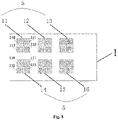
- each three modulation units 5 constitute a row, and there are two rows in total.
- a first modulation unit 11, a second modulation unit 12 and a third modulation unit 13 are arranged in the first row, and a fourth modulation unit 14, a fifth modulation unit 15 and a sixth modulation unit 16 are correspondingly arranged in the second row.
- each modulation unit is further divided into four modulation subunits, that is, a first subunit 110 located at an upper left corner of the unit matrix, a second subunit 111 located at an upper right corner of the unit matrix, a third subunit 112 located at an lower left corner of the unit matrix and a fourth subunit 113 located at an lower right corner of the unit matrix.
- the modulation holes of the modulation subunits in a same region on each modulation unit 5 have the same structural parameters and arrangement periods.
- the modulation holes 6 inside the first modulation subunit 110 and the second modulation subunit 111 are circular but have different inner diameters. Therefore, the first modulation subunit 110 has a first modulating mode with respect to the input spectrum, and the second modulation subunit 111 has a second modulating mode with respect to the input spectrum.
- the modulation holes 6 inside the third modulation subunit 112 are oval, and the third modulation subunit 112 has a third modulating mode with respect to the input spectrum.
- the modulation holes 6 in the fourth modulation subunit 113 are triangle, and the respective modulation holes 6 in the fourth modulation subunit 113 are arranged periodically row by row and column by column according to the sizes of the structural parameters, and the fourth modulation subunit 113 has a fourth modulating mode with respect to the input spectrum.
- the modulation subunits at a same position in different modulation units 5 have a same structure, but the modulation subunits at different positions are different from each other. Therefore, each of the modulation subunits has different modulating role on the same incident light.
- Each of the modulation subunits respectively corresponds to one sensing subunit on the image sensing layer 2.
- the "a certain modulating mode for light having different wavelengths" in this embodiment may include, but is not limited to, effects such as scattering, absorption, transmission, reflection, interference, surface plasmon polariton, resonance and etc.
- the first, second and third light modulating methods are different from each other.
- the modulation role can be changed by adjusting the structural parameters of the modulation holes 6 inside each modulation unit 5.
- the adjustment of the structural parameters includes, but is not limited to one of the various parameters of the two-dimensional graphic structure, such as the arrangement period of the modulation holes, modulation hole radius, side length, duty ratio, and thickness of the modulation unit, and etc, or any combination thereof.
- the duty ratio refers to a ratio of the area of the modulation holes 6 to the total area of the modulation unit 5.
- the optical modulation layer 1 is made of a silicon nitride flat plate having a thickness of 200 nm to 500 nm.
- the optical modulation layer 1 is provided with 1000 to 250000 modulation units 5 in total, and each of the modulation units 5 has an area range from 200 ⁇ m 2 to 40000 ⁇ m 2 .
- Various geometrical shapes are selected inside each modulation unit 5 as the specific cross-sectional shapes of the modulation holes 6.
- Each modulation unit 5 has a periodic arrangement of the same shape, and its duty ratio is 10% to 90%.
- the remaining structures are the same as those of Embodiment I or Embodiment II.
- Each modulation unit 5 forms one pixel point along with a sensing unit below it.
- the intensity distribution of each wavelength on a pixel point can be obtained by an algorithm.
- the structures, principles, object imaging recognition methods and chip preparation methods of the image collection chip 300 and the object imaging recognition device of Embodiment IV are basically the same as those in Embodiment III, and the same contents are not described repeatedly.
- the difference lies in that: no modulation hole 6 is provided inside the modulation subunits on a same region of each modulation unit 5.
- the first modulation subunit 110, the second modulation subunit 111 and the third modulation subunit 112 respectively corresponds to light having a specific wavelength, and has a narrow-band filtering function.
- no modulation hole 6 is provided in the fourth modulation subunit 113 so that the incident light directly passes through the region of the fourth modulation subunit 113.
- a corresponding sensing subunit is provided below each modulation subunit.
- the light intensity is respectively detected by the light sensors inside the corresponding sensing subunits. Since the light passing through the fourth modulation subunit 113 is not subjected to the narrow-band filtering, the light intensity detected by the corresponding sensing subunit 9 can be taken as a reference item.
- a differential processing is performed on the first three sets of light intensities and the fourth set of light intensity, respectively, so that the light intensity of each wavelength after narrow-band filtering can be obtained.
- the boundary of the object can also be located.
- the micro integrated image collection chip 300 of this embodiment may apply the modulation units 5 of Embodiment I, the modulation units 5 of Embodiment II, the modulation units 5 of Embodiment III or any combination of the modulation units 5 of Embodiment I, Embodiment II and Embodiment III.
- this embodiment V provides an image collection chip 300, an object imaging recognition device and an object imaging recognition method.
- the same contents between embodiment V and the various embodiments above are not described repeatedly, and the difference lies in that:
- the image collection chip 300 in embodiment V further includes a light-transmitting medium layer 4 located between the optical modulation layer 1 and the image sensing layer 2.
- the light-transmitting medium layer 4 has a thickness of 50 nm to 1 ⁇ m, and may be made of silicon dioxide.
- the light-transmitting medium layer 4 may be covered on an image sensing layer 2 by chemical vapor deposition, sputtering, and spin coating, then the deposition and etching of the optical modulation layer 1 may be performed on the top of the light-transmitting medium layer 4.
- silicon dioxide can be used as a preparation substrate for the optical modulation layer 1, and the optical modulation layer 1 is prepared by directly processing on an upper half of the substrate with micro-nano drilling, then a lower half of the silicon dioxide substrate is directly used as the light-transmitting medium layer 4, and the prepared optical modulation layer 1 and the light-transmitting medium layer 4 are transferred to the image sensing layer 2 as a whole.
- the light-transmitting medium layer 4 of this embodiment may also be set as that: the optical modulation layer 1 above the image sensing layer 2 as a whole is supported through an external support structure, so that the optical modulation layer is suspended with respect to the image sensing layer 2. As a result, an air portion between the optical modulation layer 1 and the image sensing layer 2 is the light-transmitting medium layer 4.
- this embodiment VI further provides an image collection chip 300, an object imaging recognition device and an object imaging recognition method.
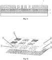
- the same contents between embodiment VI and the various embodiments above are not described repeatedly, and the difference lies in that: as shown in Fig. 11 , in the image collection chip 300 of embodiment VI, respective modulation holes 6 do not penetrate the optical modulation layer. It can be understood that, whether the modulation hole 6 penetrates the optical modulation layer or not will have no adverse effect on the modulation role of the optical modulation layer 1. This is because that the silicon-based material or other materials selected for the optical modulation layer 1 are light-transmitting materials. When a spectrum is incident into the optical modulation layer 1, a modulation role occurs due to the effect of the structure of the respective modulation units 5, but the bottom of the modulation holes 6 has no adverse effect on the spectrum modulation.
- a thickness from the bottom of the modulation holes 6 of the optical modulation layer 1 to the bottom of the optical modulation layer is 60 nm to 1200 nm, and the thickness of the entire optical modulation layer is 120 nm to 2000 nm.
- this embodiment VII further provides an image collection chip 300, an object imaging recognition device and an object imaging recognition method.
- the same contents between embodiment VII and the various embodiments above are not described repeatedly, and the difference lies in that: as shown in Fig. 12 and Fig. 13 , in the image collection chip 300 of this embodiment, six modulation units 5 which are a first modulation unit 11, a second modulation unit 12, a third modulation unit 13, a fourth modulation unit 14, a fifth modulation unit 15 and a sixth modulation unit 16, respectively, are distributed on the optical modulation layer 1.
- the first modulation unit 11, the third modulation unit 13 and the fourth modulation unit 14 are arranged according to the periodic structure of the modulation unit 5 of Embodiment III, and the second modulation unit 12, the fifth modulation unit 15 and the sixth modulation unit 16 are arranged according to the gradual structure of the modulation unit 5 of Embodiment I.
- the structural arrangement of any suitable modulation unit 5 in Embodiment I to Embodiment IV may also be selected as the modulation unit 5 at the corresponding position according to the spectral modulation needs.
- the optical modulation layer 1 of embodiment VII uses the differences in the specific cross-sectional shapes of different modulation holes 6 among different units, and the specific arrangement of the modulation holes 6 in a same unit, to perform different modulation roles on the spectrum with different wavelengths by adjusting the specific cross-sectional shapes of the modulation holes 6, the structural parameters of the modulation holes 6 and the arrangement period of the modulation holes 6.
- the modulation units 5 arbitrarily divided have different modulating roles on the spectrum.
- an infinite number of modulated spectrum samples can be obtained, which dramatically increases the amount of data for reconstructing the original spectrum, and is helpful for restoring the spectral pattern of the broadband spectrum.
- the structures of the periodic modulation units 5 of Embodiment III and Embodiment IV can generate the dispersion and resonance effects of the two-dimensional period.
- the resonance effect includes, but is not limited to, the principles of energy band control of photonic crystal, resonance of the two-dimensional grating and etc.
- the detection accuracy for specific wavelengths can be enhanced through resonance.
- the two advantages above can be integrated.
- the image collection chip 300 of the four embodiments above can be prepared into a structure of the order of micrometers or even smaller, which is of great significance for the miniaturization and micromation manufacture and use of the image collection chip 300.
- the overall size of the chip 300 is equivalent to that of a camera module, which can be smaller than 1cm ⁇ 1cm ⁇ 0.4cm.
- the chip 300 can be integrated on portable mobile devices such as mobile phones and bracelets.
- the above-mentioned optical modulation layer 1 can cooperate with the image sensing layer 2 composed of different image sensors, to achieve the full-band spectral detection in principle, so that the wide-spectrum detection performance of the image collection chip 300 is more excellent.
- this embodiment VIII further provides a micro imaging collection chip 300, a spectral imaging device and a spectral imaging method.
- the target object 2 can be expanded into any object.
- a light source 100 having a broad spectrum from visible light to near infrared is irradiated onto the target object 200, and then the reflected light is collected by the image collection chip 300.
- the light source 100 is omitted, and the target object 200 directly emits light to the image collection chip 300 for being collected by the same.
- the incident light is incident into the optical modulation layer 1 and modulated by each of the modulation units 5.
- the transmission spectra are also different.
- a plurality of sensing units 7 on the image sensing layer 2 are disposed correspondingly below each modulation unit, and as shown in Fig. 4 and Fig. 5 , under the corresponding action of multiple sets of pixel confirmation modules, the respective regions in each modulation unit 5 in Fig. 4 respectively correspond to the respective sensing subunits 9 in each sensing unit 7 in Fig. 5 .
- each sensing subunit 9 the transmission spectrum obtained by each sensing subunit 9 is different, so that each modulation subunit and each sensing subunit 9 can form a set of pixel confirmation submodules, and each of the submodules can respectively recognize a part of the spectrum information in a pixel point, thus the submodules in the respective regions can be integrated to obtain multiple spectrum information of the pixel point.
- the respective pixel points can be further integrated to obtain all the pixel points of the image and the target object image can be reconstructed accordingly.
- the two-dimensional graphic structures on the modulation unit corresponding to the respective sensing subunits 9 are the same, and the target object image at a same frequency can be obtained by obtaining the response of light in different spatial positions of the image after the light is subjected to the same modulation roles.
- the image collection chip 300 of the various embodiments of the present disclosure includes an optical modulation layer 1, an image sensing layer 2 and at least two sets of pixel confirmation modules.
- the optical modulation layer 1 is located on the image sensing layer 2, and each set of the pixel confirmation modules includes modulation units 5 and sensing units 7.
- Each modulation unit 5 and each sensing unit 7 are correspondingly provided up and down on the optical modulation layer 1 and the image sensing layer 2, respectively.
- the light intensity of the spectrum is sensed and detected by each set of the pixel confirmation modules respectively, so that the pixel data of respective pixel points is respectively determined, thereby integrating all the pixel data to form the final output image.
- the image collection chip 300 can replace the complicated and precise beam splitting elements and excessive image sensors in the existing object imaging recognition devices, and use modulation units 5 and sensing units 7 to modulate the spectra and sense the light intensity respectively, thereby achieving an accurate image reconstruction process, enabling the image collection chip 300 to perform light intensity sensing without gratings, prisms, reflectors, or other similar spatial beam splitting elements, thereby greatly reducing the volume of the object imaging recognition device and at the same time improving the precision of the light intensity sensing, so that the object imaging recognition device has the advantages of high measurement accuracy, good portability, real-time on-line detection, simple operation, stable performance, low manufacturing cost and etc.
- each modulation unit is provided with at least one modulation subunit, and each of the modulation subunits is respectively provided with several modulation holes 6 penetrating into the optical modulation layer 1, and respective modulation holes 6 in a same modulation subunit are arranged into a two-dimensional graphic structure with a specific pattern.
- the chip 300 may collect image information of an object to be imaged of multiple spectra simultaneously on a basis that an array of modulation units 5 has the modulation role on light having different wavelengths in optoelectronics and each modulation unit 5 is correspondingly nested with a plurality of modulation subunits, which greatly improves the spectral recognition rate and reduces the rate of mis-recognition.
- the chip 300 can be applicable for biological iris recognition to facilitate the living organism detection for anti-counterfeiting, and increase the difficulty in cracking and forgery. At the same time, the chip 300 can also reduce the interference caused by contact lenses, cosmetic contact lenses and different lighting conditions, and overcome the problem that the existing object imaging recognition device is expensive and cannot be miniaturized.
- both “a plurality of' and “several” means two or more; unless specified otherwise, “notch” means the shapes other than the shape with a flush cross section.
- the orientation or position relations indicated by the terms “upper”, “lower”, “left”, “right”, “inner”, “outer”, “front end”, “rear end”, “head portion”, “tail portion” etc. are based on the orientation or position relations shown in the drawings, which is merely for the convenience of describing the present disclosure and simplifying the description, and is not to indicate or imply that the device or component referred to must have a specific orientation, be constructed and operated in the specific orientation. Therefore, it cannot be construed as limiting the present disclosure.
- the terms “first”, “second” and “third” etc. are for the purpose of description, and cannot be construed as indicating or implying the relative importance.
- the terms “mount”, “connect with”, and “connect to” should be understood in a broad sense, for example, they may be fixed connections or may be removable connections, or integrated connections; may be mechanical connections or electrical connections; may be direct connections or indirect connections through intermediate mediums.
- the specific meanings of the terms above in the present disclosure can be understood according to specific situations.
Landscapes
- Physics & Mathematics (AREA)
- Spectroscopy & Molecular Physics (AREA)
- Engineering & Computer Science (AREA)
- Signal Processing (AREA)
- General Physics & Mathematics (AREA)
- Computer Networks & Wireless Communication (AREA)
- Electromagnetism (AREA)
- Multimedia (AREA)
- Optics & Photonics (AREA)
- Investigating Or Analysing Materials By Optical Means (AREA)
- Transforming Light Signals Into Electric Signals (AREA)
- Studio Devices (AREA)
- Die Bonding (AREA)
- Solid State Image Pick-Up Elements (AREA)
Abstract
Description
- The present application claims priority to
Chinese Patent Application No. 201910700328.7, filed on July 31, 2019 - The present application relates to the technical fields of imaging and object recognition devices, and particularly to an image collection chip, an object imaging recognition device and an object imaging recognition method.
- Imaging spectroscopy is a technology that organically combines spectral detection and imaging, and can image an object in different spectra, and simultaneously obtain the geometric shape information and spectral characteristics of the detected object. It is also a technology to obtain many very narrow and spectrally continuous image data of ultraviolet, visible, near infrared and mid-infrared regions of electromagnetic waves. Through more than 30 years of development, imaging spectroscopy has become an important means for earth observation and deep space exploration, and has been widely applied in the fields of agriculture, animal husbandry and forestry production, mineral resource exploration, cultural relic detection, marine remote sensing, environmental monitoring, disaster prevention and mitigation, military reconnaissance and etc.
- With the gradual miniaturization of carrying platforms, such as small platforms of small satellites, unmanned aerial vehicle and etc., and the endurance requirement of field applications, the demand for miniaturization and lightweight of image collection devices has become increasingly prominent. A conventional image collection device is usually an imaging spectrometer. The imaging spectrometers have three imaging types in which the opto-mechanical scanning type has moving parts and is heavy and bulky; the push-broom imaging type has a complicated optical system; and the staring imaging type has limited spatial resolution and number of spectral channels. All three types fail to meet the demands for miniaturization and lightweight.
- The embodiments of the present disclosure provide an image collection chip, an object imaging recognition device and an object imaging recognition method for overcoming the defect that the imaging spectrometers of the existing image collection devices fail to meet the requirements of miniaturization and lightweight.
- In order to solve the technical problem above, the disclosure provides an image collection chip, including an optical modulation layer, an image sensing layer and at least two sets of pixel confirmation modules; wherein, the optical modulation layer is located on the image sensing layer, and each set of the pixel confirmation modules includes modulation units and sensing units; each modulation unit and each sensing unit are correspondingly provided up and down on the optical modulation layer and the image sensing layer, respectively; wherein, each modulation unit is provided with at least one modulation subunit, and each of the modulation subunits is provided with several modulation holes penetrating into the optical modulation layer; the respective modulation holes inside a same modulation subunit are arranged into a two-dimensional graphic structure having a specific pattern.
- In some embodiments, the specific pattern of the two-dimensional graphic structure includes that:
- all the modulation holes inside a same two-dimensional graphic structure have a same specific cross-sectional shape and the respective modulation holes are arranged in an array in an order that sizes of structural parameters are gradually varied; and/or
- the respective modulation holes inside a same two-dimensional graphic structure respectively have a specific cross-sectional shape and the respective modulation holes are combined and arranged according to the specific cross-sectional shape.
- In some embodiments, the arrangement order is being arranged row by row or column by column according to a preset period order when the respective modulation holes are arranged and combined according to the specific cross-sectional shape.
- In some embodiments, no modulation holes are provided in the modulation subunit at a same position in each of the modulation units.
- In some embodiments, a bottom of the modulation hole penetrates the optical modulation layer or does not penetrate the optical modulation layer.
- In some embodiments, the image collection chip further includes a signal processing circuit layer connected below the image sensing layer and configure to electrically connect each of the sensing units.
- In some embodiments, the sensing unit includes at least one sensing subunit; respective sensing subunits are arranged in an array, and each of the sensing subunits is provided with at least one image sensor; all of the sensing subunits are electrically connected through the signal processing circuit layer.
- In some embodiments, the image collection chip further includes a light-transmitting medium layer between the optical modulation layer and the image sensing layer.
- The present disclosure also provides an object imaging recognition device, including:
- a light source configured to emit spectra to an object to be imaged, so that the spectra are incident on an image collection chip as incident light after passing through the object to be imaged; and
- the image collection chip as described above provided on a same side of the object to be imaged along with the light source; wherein, the image collection chip is configured to perform light modulation on the incident light by using each set of the pixel confirmation modules to obtain at least two modulated spectra, and to sense and detect light intensity of each of the modulated spectra respectively to determine pixel data of respective pixel points respectively.
- The present disclosure also provides an object imaging recognition method based on the object imaging recognition device as described above; the imaging recognition method includes:
- emitting spectra to an object to be imaged using a light source, so that the spectra are incident on the image collection chip as incident light after the spectra pass through the object to be imaged; and
- performing light modulation on the incident light using each set of pixel confirmation modules of the image collection chip respectively so as to obtain several modulated spectra, and sensing and detecting the light intensity of each of the modulated spectra respectively to determine each set of pixel data; and
- integrating all the pixel data to form an output image.
- The technical solutions above of the present disclosure have the following advantageous effects:
- 1. The image collection chip of the present disclosure includes an optical modulation layer, an image sensing layer and at least two sets of pixel confirmation modules. The optical modulation layer is located on the image sensing layer, and each set of the pixel confirmation modules includes modulation units and sensing units. Each modulation unit and each sensing unit are correspondingly provided up and down on the optical modulation layer and the image sensing layer respectively. The light intensity of the spectrum is sensed and detected by each set of the pixel confirmation modules respectively, so that the pixel data of respective pixel points is respectively determined, and then all the pixel data is integrated to form a final output image. The image collection chip can replace the complicated and precise beam splitting elements and excessive image sensors in the existing object imaging recognition devices, and use modulation units and sensing units to modulate the spectra and sense the light intensity respectively, thereby achieving an accurate image reconstruction process, enabling the image collection chip to perform light intensity sensing without gratings, prisms, reflectors, or other similar spatial beam splitting elements, thereby greatly reducing the volume of the object imaging recognition device and at the same time improving the precision of the light intensity sensing, so that the object imaging recognition device has the advantages of high measurement accuracy, good portability, real-time on-line detection, simple operation, stable performance, low manufacturing cost and etc. The chip has broad prospects for applications on small platforms such as small satellites, unmanned aerial vehicle and etc.
- 2. In the image collection chip, each modulation unit is provided with at least one modulation subunit, each of the modulation subunits is provided with several modulation holes penetrating into the optical modulation layer, and respective modulation holes in a same modulation subunit are arranged into a two-dimensional graphic structure with a specific pattern. The chip is on a basis that an array of modulation units has the modulation role on light having different wavelengths in optoelectronics, and each modulation unit is correspondingly nested with a plurality of modulation subunits, so that image information of an object to be imaged of multiple spectra may be collected simultaneously, which greatly improves the spectral recognition rate and reduces the rate of mis-recognition. The chip can be applicable for iris recognition and improve the recognition rate by simultaneously obtaining iris image information under a plurality of wavelengths, and the chip can facilitate the living organism detection for anti-counterfeiting, and increase the difficulty in cracking and forgery. At the same time, the chip can also reduce the interference caused by contact lenses, cosmetic contact lenses and different lighting conditions. The chip overcomes the problem that the existing object imaging recognition device is expensive and cannot be miniaturized.
- For more clearly illustrating the embodiments of the present disclosure or the technical solutions in the prior art, the drawings to be used in describing the embodiments or the prior art will be briefly described below. Obviously, the drawings in the following description are some embodiments of the present disclosure, for those of ordinary skill in the art, other drawings may also be obtained based on these drawings without any creative work.
-
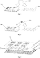
Fig. 1 is a diagram showing an imaging principle of an object imaging recognition device according to an embodiment of the present disclosure; -
Fig. 2 is a diagram showing a working principle of the object imaging recognition device imaging an iris according to an embodiment of the present disclosure; -
Fig. 3 is a structural schematic diagram of the image collection chip of Embodiment I of the present disclosure; -
Fig. 4 is a sectional view of the image collection chip of Embodiment I of the present disclosure; -
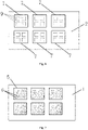
Fig. 5 is a schematic diagram of an optical modulation layer of Embodiment I of the present disclosure; -
Fig. 6 is a structural schematic diagram of an image sensing layer of Embodiment I of the present disclosure; -
Fig. 7 is a structural schematic diagram of an optical modulation layer of Embodiment II of the present disclosure; -
Fig. 8 is a structural schematic diagram of an optical modulation layer of Embodiment III of the present disclosure; -
Fig. 9 is a structural schematic diagram of an optical modulation layer of Embodiment IV of the present disclosure; -
Fig. 10 is a sectional view of an image collection chip of Embodiment V of the present disclosure; -
Fig. 11 is a sectional view of an image collection chip of Embodiment VI of the present disclosure; -
Fig. 12 is a structural schematic diagram of an image collection chip of Embodiment VII of the present disclosure; -
Fig. 13 is a structural schematic diagram of an optical modulation layer of Embodiment VII of the present disclosure; and -
Fig. 14 and Fig. 15 are respectively process diagrams illustrating the methods for preparaing and processing the modulation holes of the image collection chip of Embodiment I to Embodiment VII of the present disclosure. -
100 light source 200 object to be imaged 300 image collection chip 1' substrate 1 optical modulation layer 2 image sensing layer 3 signal processing circuit layer 4 light-transmitting medium layer 5 modulation unit 6 modulation hole 7 sensing unit 8 gap 9 sensing subunit 11 first modulation unit 12 second modulation unit 13 third modulation unit 14 fourth modulation unit 15 fifth modulation unit 16 sixth modulation unit 110 first subunit 111 second subunit 112 third subunit 113 fourth subunit - Implementations of the present disclosure are further described below in detail with reference to the accompanying drawings and embodiments. The following embodiments are used to illustrate the present disclosure, but cannot be used to limit the scope thereof. Unless specified otherwise, the chips mentioned in the present disclosure are all abbreviations for the imaging collection chip.
- The various embodiments of the present disclosure provide an image collection chip that can replace the complicated and precise beam splitting elements and excessive image sensors in the existing object imaging recognition devices, and simultaneously modulate multiple spectra and sense the light intensity respectively using modulation units and sensing units, thereby achieving an accurate image reconstruction process, enabling the image collection chip to perform light intensity sensing operation without gratings, prisms, reflectors, or other similar spatial beam splitting elements, thereby greatly reducing the volume of the object imaging recognition device and at the same time improving the precision of the light intensity sensing, so that the object imaging recognition device has the advantages of high measurement accuracy, good portability, real-time on-line detection, simple operation, stable performance, low manufacturing cost and etc.
- Specifically, as shown in
Fig. 1 to Fig. 3 , thechip 300 includes anoptical modulation layer 1, animage sensing layer 2, and at least two sets of pixel confirmation modules. Theoptical modulation layer 1 is located on theimage sensing layer 2 and configured to receive incident light and modulate the incident light, and theimage sensing layer 2 is configured to sense light intensities of modulated spectra, so as to determine corresponding image pixel data with respect to the light intensity of the spectrum having different wavelengths. Each set of the pixel confirmation modules includesmodulation units 5 andsensing units 7, correspondingly, each set of themodulation unit 5 and thesensing unit 7 are correspondingly provided up and down on theoptical modulation layer 1 and theimage sensing layer 2 respectively, so that eachmodulation unit 5 and eachsensing unit 7 can determine at least one set of image pixel data correspondingly. The original output image is reconstructed by integrating all the image pixel data. - In this embodiment, each
modulation unit 5 is provided with at least one modulation subunit, each of the modulation subunits is respectively provided withseveral modulation holes 6 penetrating into theoptical modulation layer 1, andrespective modulation holes 6 in a same modulation subunit are arranged into a two-dimensional graphic structure with a specific pattern. Theimage collection chip 300 of this embodiment can replace the precise optical components in the existing object imaging recognition devices so as to perform the precise modulation and pixel reconstruction on incident light. By using theimage collection chip 300, the modulation role on light having different wavelengths can be flexibly implemented. The modulation role includes, but is not limited to, the scattering, absorption, projection, reflection, interference, surface plasmon polariton, resonance and etc. of light, so as to improve differences in the spectral responses between different regions, thereby improving the analytical precision of theimage collection chip 300. In addition, thechip 300 implements the modulation role on light having different wavelengths using one or more two-dimensional graphic structures on eachmodulation unit 5, and the differences between two-dimensional graphic structures can also improve the differences in spectral responses between different regions, thereby improving the analytical precision of theimage collection chip 300. - The
chip 300 of this embodiment further includes a signalprocessing circuit layer 3 connected under theimage sensing layer 2 and configured to electrically connect each of thesensing units 7, so that the differential responses can be calculated according to the light intensity sensed by each set of the pixel confirmation modules. Since the sensors inside eachsensing unit 7 can form a pixel point according to the sensed light intensity, the intensity distribution of each wavelength on one pixel can be obtained through an algorithm. The differential responses refer to calculating a difference value between a signal of a responsive spectrum obtained after modulation by the optical modulation layer and a signal of an original spectrum, or calculating difference values between signals of responsive spectra obtained after modulation by each of themodulation units 5, or calculating difference values between signals of responsive spectra obtained after modulation by each of the modulation subunits. The original spectra refer to spectra of the incident light entering the optical modulation layer. - Furhter, each
sensing unit 7 includes at least onesensing subunit 9, and therespective sensing subunits 9 are arranged in an array. Each of thesensing subunits 9 is provided with at least one image sensor, and all of thesensing subunits 9 are electrically connected through the signalprocessing circuit layer 3, so as to distinguish the pixel points formed on themodulation units 5 and thesensing units 7 of different sets more carefully, thereby using a plurality of pixel points generated by the modulation subunits of a same position in each set and the correspondingsensing subunits 9 to constitute an image containing pieces of spectral information. - As shown in
Fig. 1 , bases on the various embodiments of the present disclosure, an object imaging recognition device is provided. The device includes alight source 100 and animage collection chip 300. Thelight source 100 is configured to emit spectra to an object to be imaged 200, so that the spectra are incident on theimage collection chip 300 as incident light after passing through the object to be imaged 200. Theimage collection chip 300 and thelight source 100 are simultaneously disposed on a same side of the object to be imaged 200. Theimage collection chip 300 is configured to perform light modulation on the incident light by using each set of the pixel confirmation modules to obtain at least two modulated spectra, and to sense and detect the light intensity of respective modulated spectra respectively to determine each of the pixel points, so that all of the pixels are finally integrated to form an image. - For facilitating the spectra of the
light source 100 to pass through the object to be imaged 200 so that the reflected light formed is used as the incident light of thechip 300, it is preferable to simultaneously arrange thelight source 100 and theimage collection chip 300 on a same side of the object to be imaged 200. TakingFig. 2 as an example, thelight source 100 and theimage collection chip 300 are simultaneously disposed at a lower side of the object to be imaged 200. The spectra of visible-near infrared light generated by thelight source 100 can penetrate inside the object to be imaged 200 using the light reflection principle, and all of the spectra form incident light incident on theimage collection chip 300 under the act of reflection. This structural arrangement can expand the testing space and improve the convenience in object imaging and recognition. -
Fig. 2 shows a diagram illustrating imaging principle of the object imaging recognition device according to the present disclosure applied to image aniris 210. It can be appreciated that, theimage collection chip 300 and the object imaging recognition device described in the present disclosure can perform imaging recognition not only on theiris 210, but also on any other object to be imaged 200. It is only needed to adjust the parameters such as the volume of eachmodulation unit 5 of theimage collection chip 300, the corresponding wavelengths of the incident light and etc. according to the imaging needs. - Hereinafter, the
iris 210 is taken as an object to be imaged as an example, and theimage collection chip 300 and the object imaging recognition device of the present disclosure are described in detail specifically through several embodiments. Thechips 300 described in the various embodiments below are suitable for the above-mentioned object imaging recognition device. - As shown in
Fig. 3 andFig. 4 , in theimage collection chip 300 provided by Embodiment I, theoptical modulation layer 1 includes a plurality ofmodulation units 5. All the modulation holes 6 inmodulation units 5 penetrate theoptical modulation layer 1. The two-dimensional graphic structure composed of a plurality ofmodulation holes 6 inside eachmodulation unit 5 has a same specific cross-sectional shape. Sixmodulation units 5 composed of an array ofoval modulation holes 6 shown inFig. 2 are taken as an example for describing Embodiment I. All the modulation holes 6 inside eachmodulation unit 5 are arranged in an array in an order that sizes of structural parameters are gradually varied with a same rule to form the two-dimensional graphic structure. In this two-dimensional graphic structure, all the modulation holes 6 are arranged in an array, and all the modulation holes 6 are arranged row by row and column by column in an order from small to large according to a length of a major axis, a length of a minor axis and an angle of rotation. - It can be understood that, as shown in
Fig. 5 , since all the modulation holes 6 in this embodiment are arranged according to the same pattern, that is, being gradually arranged row by row and column by column from small to large according to the structural parameters of the length of the major axis, the length of the minor axis and the angle of rotation, all the modulation holes 6 on theoptical modulation layer 1 can be regarded as anintegral modulation unit 5, and can also be further arbitrarily divided intoseveral modulation units 5. The arbitrarily dividedmodulation units 5 have different modulating roles on the spectrum. In theory, an infinite number of modulated spectrum samples can be obtained, which dramatically increases the amount of data for reconstructing the original spectrum, and is helpful for restoring the spectral pattern of the broadband spectrum. Then, the effectiveness of the modulating roles of themodulation unit 5 on the light having different wavelengths can be determined according to the structural parameter characteristics of the modulation holes 6 inside eachmodulation unit 5. The reconstructing process is implemented by a data processing module including spectral data preprocessing and a data predicting model. In this embodiment, the spectral data preprocessing refers to preprocessing noises existing in the differential response data obtained above. The processing methods used for the spectral data preprocessing include, but are not limited to, Fourier transform, differential, and wavelet transform. The data predicting model includes predictions of pattern parameters of the object to be imaged 200 from spectral data information. The algorithms used include, but are not limited to, least squares method, principal component analysis, and artificial neural network. - It can be understood that, in this embodiment, each
modulation unit 5 is provided up and down corresponding to onesensing unit 7, so that the image sensors inside thesensing unit 7 are used to form a pixel point with the spectrum received by themodulation unit 5, and the intensity distribution over a pixel point can be obtained through an algorithm. A plurality of pixel points formed correspondingly to different sets of pixel confirmation modules are integrated to form an image containing multiple spectrum information. - Further, since different regions (modulation subunits) divided in each
modulation unit 5 have different structural parameters, each modulation subunit has different modulation role on the light having different wavelengths, and the modulation role includes, but is not limited to, scattering, absorption, transmission, reflection, interference, polariton and etc. The final effect of modulation is to determine that the light having different wavelengths has different transmission spectra when it passes through different modulation subunit regions of eachmodulation unit 5. The same input spectrum has different transmission spectra after the input spectrum passes through different regions in a same two-dimensional graphic structure. - In this embodiment, a
sensing unit 7 is disposed correspondingly below eachmodulation unit 5, and a plurality of sensors are provided in eachsensing unit 7, as shown inFig. 6 . Each sensor in thesame sensing unit 7 respectively corresponds to a different region in thesame modulation unit 5, and each sensor and its corresponding region constitute a pixel point respectively. Therefore, each set of the pixel confirmation modules can form more than one pixel point respectively, and the intensity distribution of each wavelength on a pixel point can be obtained through an algorithm. A plurality of pixel points formed correspondingly to a same position of different sets of pixel confirmation modules are integrated to form an image containing multiple spectrum information. - It can be understood that the specific cross-sectional shape of the modulation holes 6 above includes circle, ellipse, cross, regular polygon, star, rectangle and so on, or any combination thereof. Correspondingly, the structural parameters of the modulation holes 6 above include inner diameter, length of major axis, length of minor axis, rotation angle, number of angles, side length and etc.
- The
light source 100 applicable to the object imaging recognition device described in Embodiment I is a light source from visible light to near-infrared band, and a wavelength range of thelight source 100 is 400 nm to 1100 nm. Theoptical modulation layer 1 has a thickness of 60 nm to 1200 nm. Theoptical modulation layer 1 and theimage sensing layer 2 are directly connected or connected through a light-transmittingmedium layer 4. Theimage sensing layer 2 and the signalprocessing circuit layer 3 are electrically connected. In this embodiment, as shown inFig. 5 , sixmodulation units 5 in total are arranged on theoptical modulation layer 1, and all themodulation units 5 are arranged in an array. And all the modulation holes 6 of eachmodulation unit 5 are elliptical, and lengths of minor axes of all theelliptical modulation holes 6 are increased row by row and column by column, respectively. InFig. 5 , the horizontal direction is taken as the horizontal axis, and the vertical direction is taken as the vertical axis. All theelliptical modulation holes 6 in eachmodulation unit 5 are rotated from the vertical axis to the horizontal axis row by row and column by column, and the rotation angles are gradually increased. All the modulation holes 6 in eachmodulation units 5 constitute a same two-dimensional graphic structure which is a matrix structure as a whole, and the area of the matrix structure ranges from 200 µm2 to 40000 µm2. - When the
image collection chip 300 described in this embodiment is manufactured, a silicon-based material is selected as the material of both theoptical modulation layer 1 and theimage sensing layer 2 at the same time, so as to have a good compatibility in the process of the preparation technology. When theoptical modulation layer 1 is prepared, theoptical modulation layer 1 may be directly generated on theimage sensing layer 2, or the preparedoptical modulation layer 1 may be transferred to theimage sensing layer 2 firstly. - The direct generation of the
optical modulation layer 1 specifically includes: directly growing theoptical modulation layer 1 arranged according to the structure shown inFig. 5 on theimage sensing layer 2 by a deposition; or installing a substrate made of the silicon-based material on theimage sensing layer 2, then performing micro-nano processing and perforating on the substrate according to the structure shown inFig. 5 to obtain theoptical modulation layer 1. - The process of the directly growing by the deposition above is: Step one, a silicon flat panel is deposited on the
image sensing layer 2 through sputtering, chemical vapor deposition and etc. Step two, the desired two-dimensional graphic structure as shown inFig. 6 is drawn on the silicon flat panel by using a pattern transfer method such as photoetching, electron beam exposure and etc. The two-dimensional graphic structure is specifically that, only the minor axes and the rotation angles of theelliptical modulation holes 6 are gradually adjusted. The major axis of the ellipse is selected from a fixed value in the range of 200 nm to 1000 nm, for example, 500 nm; and the length of the minor axis varies within the range of 120 nm to 500 nm. The rotation angle of the ellipse varies within the range of 0° to 90°, and the arrangement period of the ellipses is a fixed value in the range of 200 nm to 1000 nm, for example, 500 nm. The pattern of themodulation unit 5 has an entire area range from 200 µm2 to 40,000 µm2 and is in a rectangular array structure. Step three, the silicon flat panel is etched through reactive ion etching, inductively coupled plasma etching, ion beam etching and etc. to obtain the desiredoptical modulation layer 1. Finally, theoptical modulation layer 1 and theimage sensing layer 2 are electrically connected as a whole to the signalprocessing circuit layer 3. - The transfer preparation method of the
optical modulation layer 1 above is specifically: firstly, performing micro-nano processing and perforating on the substrate according to the structure shown inFig. 5 to obtain the preparedoptical modulation layer 1, then transferring the preparedoptical modulation layer 1 onto theimage sensing layer 2. Specifically, the process of transferring theoptical modulation layer 1 is that, firstly preparing theoptical modulation layer 1 on a silicon wafer or SOI (referring to the silicon-on-insulator silicon wafer structure) according to the parameters above, then transferring theoptical modulation layer 1 onto theimage sensing layer 2 with transfer methods, and finally, electrically connecting theoptical modulation layer 1 and theimage sensing layer 2 as a whole to the signalprocessing circuit layer 3. - As shown in
Fig. 14 and Fig. 15 , this embodiment also provides another process for preparing theimage collection chip 300, which is specifically that theimage sensing layer 2 is equipped with a III-V group detector that is specifically a GaAs/InGaAs quantum well detector. As shown inFig. 14 , the detector is reversely bonded to a CMOS circuit. The detector includes a GaAs substrate 1' and an InGaAs quantum wellimage sensing layer 2. As shown inFig. 15 , after the substrate 1' is directly thinned, micro-nano processing is performed on the substrate 1' so as to have a two-dimensional graphic structure to form theoptical modulation layer 1. The difference between this preparation process and the above-mentioned micro-nano processing and perforating only lies in that an upper surface of theimage sensing layer 2 composed of detectors is directly used as the substrate 1' for the micro-nano processing, thereby ensuring a tight connection between the processed and preparedoptical modulation layer 1 and theimage sensing layer 2, and avoiding the appearance of gaps which affects the modulation effect of the light. - The complete process of image collection and reconstruction by the object imaging recognition device of this embodiment is as follows: as shown in
Fig. 2 , firstly, alight source 100 having a wide spectrum from visible light to near infrared is irradiated to aniris 210 of a human eye, so that theiris 210 absorbs the incident light and reflects it on thechip 300. The reflected light emitted on thechip 300 by theiris 210 is the incident light of thechip 300. Then, the incident light is incident on theoptical modulation layer 1 and modulated by each of themodulation units 5. In this process, since different regions on eachmodulation unit 5 have different modulation roles, the transmission spectra are also different. A plurality ofsensing units 7 on theimage sensing layer 2 are disposed correspondingly below each modulation unit, and as shown inFig. 4 and Fig. 5 , under the corresponding action of multiple sets of pixel confirmation modules, the respective regions of eachmodulation unit 5 inFig. 4 respectively correspond to therespective sensing subunits 9 in each ofsensing unit 7 inFig. 5 . Therefore, the transmission spectrum obtained by eachsensing subunit 9 is different, so that each modulation subunit and eachsensing subunit 9 can form a set of pixel confirmation submodules, and each submodule can respectively recognize a part of the spectrum information in a pixel point, thus the submodules in the respective regions can be integrated to obtain multiple spectrum information of the pixel point. The respective pixel points can be further integrated to obtain all the pixel points of the image and the iris image can be reconstructed accordingly. It can be understood that, since the two-dimensional graphic structures on the modulation unit corresponding to each of thesensing subunits 9 are the same, and the iris image at a same frequency can be obtained by obtaining the response of light in different spatial positions of the image after the light is subjected to the same modulation roles. - The structures, principles, object imaging recognition methods and chip preparation methods of the
image collection chip 300 and the object imaging recognition device of Embodiment II are basically the same as those in Embodiment I, and the same contents are not described repeatedly. The difference lies in that:
as shown inFig. 7 , for theimage collection chip 300 of this embodiment, in eachmodulation unit 5 provided on theoptical modulation layer 1, all the modulation holes 6 in each of the two-dimensional graphic structures respectively have specific cross-sectional shapes, and therespective modulation holes 6 are freely combined and arranged (i.e., arranged arbitrarily without rules) according to the specific cross-sectional shapes. Specifically, in the two-dimensional graphic structure, some of the modulation holes 6 have the same specific cross-sectional shapes, and therespective modulation holes 6 having the same specific cross-sectional shape constitute a plurality ofmodulation hole 6 groups, and each of themodulation hole 6 groups has specific cross-sectional shapes different form each other, and all the modulation holes 6 are freely combined. - It can be understood that, the
modulation units 5 as a whole can be regarded as modulating a spectrum having a specific wavelength, or can be freely divided into several micro-nano modulation subunits, so as to be able to modulate the spectrum having multiple different wavelengths, thereby increasing the flexibility and diversity of light modulation. - The structures, principles, object imaging recognition methods and chip preparation methods of the
image collection chip 300 and the object imaging recognition device of Embodiment III are basically the same as those in Embodiment II, and the same contents are not described repeatedly. The difference lies in that:
two ormore modulation units 5 are arranged on theoptical modulation layer 1 of theimage collection chip 300 in this embodiment, and eachmodulation unit 5 is further divided into at least two modulation subunits. All the modulation holes 6 in each modulation subunit are respectively combined and arranged according to the specific cross-sectional shape, and the arrangement order is being arranged row by row or column by column according to a preset periodic order. The modulation holes 6 of the modulation subunits inside a same region of eachmodulation unit 5 have the same cross-sectional shape and arrangement period. Therefore, the modulation subunits at different positions of eachmodulation unit 5 have different modulation roles on the same incident light. By changing the gradual order of the structural parameters of the modulation holes 6 inside themodulation units 5 and/or the specific cross-sectional shapes of the modulation holes 6 according to the modulation requirement, the modulation role and/or the modulated object of thecurrent modulation unit 5 can be changed. - Specifically, as shown in
Fig. 8 , sixmodulation units 5 are distributed on theoptical modulation layer 1, each threemodulation units 5 constitute a row, and there are two rows in total. Specifically, afirst modulation unit 11, asecond modulation unit 12 and athird modulation unit 13 are arranged in the first row, and afourth modulation unit 14, afifth modulation unit 15 and asixth modulation unit 16 are correspondingly arranged in the second row. According to a same structure ratio, each modulation unit is further divided into four modulation subunits, that is, afirst subunit 110 located at an upper left corner of the unit matrix, asecond subunit 111 located at an upper right corner of the unit matrix, athird subunit 112 located at an lower left corner of the unit matrix and afourth subunit 113 located at an lower right corner of the unit matrix. - In this embodiment, the modulation holes of the modulation subunits in a same region on each
modulation unit 5 have the same structural parameters and arrangement periods. Specifically, the modulation holes 6 inside thefirst modulation subunit 110 and thesecond modulation subunit 111 are circular but have different inner diameters. Therefore, thefirst modulation subunit 110 has a first modulating mode with respect to the input spectrum, and thesecond modulation subunit 111 has a second modulating mode with respect to the input spectrum. The modulation holes 6 inside thethird modulation subunit 112 are oval, and thethird modulation subunit 112 has a third modulating mode with respect to the input spectrum. The modulation holes 6 in thefourth modulation subunit 113 are triangle, and therespective modulation holes 6 in thefourth modulation subunit 113 are arranged periodically row by row and column by column according to the sizes of the structural parameters, and thefourth modulation subunit 113 has a fourth modulating mode with respect to the input spectrum. The modulation subunits at a same position indifferent modulation units 5 have a same structure, but the modulation subunits at different positions are different from each other. Therefore, each of the modulation subunits has different modulating role on the same incident light. Each of the modulation subunits respectively corresponds to one sensing subunit on theimage sensing layer 2. - It can be understood that, the "a certain modulating mode for light having different wavelengths" in this embodiment may include, but is not limited to, effects such as scattering, absorption, transmission, reflection, interference, surface plasmon polariton, resonance and etc. The first, second and third light modulating methods are different from each other. By the arrangements of the modulation holes 6 inside the
modulation units 5, differences in the spectral response between different units can be improved, and by increasing the number of the units, the sensitivity to the differences between different spectra can be improved. - It can be understood that, for measuring different incident spectra, the modulation role can be changed by adjusting the structural parameters of the modulation holes 6 inside each
modulation unit 5. The adjustment of the structural parameters includes, but is not limited to one of the various parameters of the two-dimensional graphic structure, such as the arrangement period of the modulation holes, modulation hole radius, side length, duty ratio, and thickness of the modulation unit, and etc, or any combination thereof. In this embodiment, the duty ratio refers to a ratio of the area of the modulation holes 6 to the total area of themodulation unit 5. - In this embodiment, the
optical modulation layer 1 is made of a silicon nitride flat plate having a thickness of 200 nm to 500 nm. Theoptical modulation layer 1 is provided with 1000 to 250000modulation units 5 in total, and each of themodulation units 5 has an area range from 200 µm2 to 40000 µm2. Various geometrical shapes are selected inside eachmodulation unit 5 as the specific cross-sectional shapes of the modulation holes 6. Eachmodulation unit 5 has a periodic arrangement of the same shape, and its duty ratio is 10% to 90%. The remaining structures are the same as those of Embodiment I or Embodiment II. - Each
modulation unit 5 forms one pixel point along with a sensing unit below it. The intensity distribution of each wavelength on a pixel point can be obtained by an algorithm. By integrating images of the pixel points constituted by the submodules at a same position of different units under a same modulation mode, a plurality of pixel points constitute an image containing multiple spectrum information. - The structures, principles, object imaging recognition methods and chip preparation methods of the
image collection chip 300 and the object imaging recognition device of Embodiment IV are basically the same as those in Embodiment III, and the same contents are not described repeatedly. The difference lies in that: nomodulation hole 6 is provided inside the modulation subunits on a same region of eachmodulation unit 5. TakingFig. 9 as an example, thefirst modulation subunit 110, thesecond modulation subunit 111 and thethird modulation subunit 112 respectively corresponds to light having a specific wavelength, and has a narrow-band filtering function. And nomodulation hole 6 is provided in thefourth modulation subunit 113 so that the incident light directly passes through the region of thefourth modulation subunit 113. - Correspondingly, a corresponding sensing subunit is provided below each modulation subunit. After the light is subjected to narrow-band filtering of the
first modulation subunit 110, thesecond modulation subunit 111 and thethird modulation subunit 112, the light intensity is respectively detected by the light sensors inside the corresponding sensing subunits. Since the light passing through thefourth modulation subunit 113 is not subjected to the narrow-band filtering, the light intensity detected by the correspondingsensing subunit 9 can be taken as a reference item. A differential processing is performed on the first three sets of light intensities and the fourth set of light intensity, respectively, so that the light intensity of each wavelength after narrow-band filtering can be obtained. In addition, by arranging thefourth modulation subunit 113, the boundary of the object can also be located. - It can be understood that, the micro integrated
image collection chip 300 of this embodiment may apply themodulation units 5 of Embodiment I, themodulation units 5 of Embodiment II, themodulation units 5 of Embodiment III or any combination of themodulation units 5 of Embodiment I, Embodiment II and Embodiment III. - Based on the structures, principles, object imaging recognition methods and chip preparation methods of the
image collection chip 300 and the object imaging recognition device of any of the embodiments above, this embodiment V provides animage collection chip 300, an object imaging recognition device and an object imaging recognition method. The same contents between embodiment V and the various embodiments above are not described repeatedly, and the difference lies in that: - As shown in
Fig. 10 , theimage collection chip 300 in embodiment V further includes a light-transmittingmedium layer 4 located between theoptical modulation layer 1 and theimage sensing layer 2. Specifically, the light-transmittingmedium layer 4 has a thickness of 50 nm to 1 µm, and may be made of silicon dioxide. - In the
image collection chip 300 of this embodiment, when a process scheme of directly growing by deposition is applied in the preparation of theoptical modulation layer 1, the light-transmittingmedium layer 4 may be covered on animage sensing layer 2 by chemical vapor deposition, sputtering, and spin coating, then the deposition and etching of theoptical modulation layer 1 may be performed on the top of the light-transmittingmedium layer 4. When a transfer process scheme is applied, silicon dioxide can be used as a preparation substrate for theoptical modulation layer 1, and theoptical modulation layer 1 is prepared by directly processing on an upper half of the substrate with micro-nano drilling, then a lower half of the silicon dioxide substrate is directly used as the light-transmittingmedium layer 4, and the preparedoptical modulation layer 1 and the light-transmittingmedium layer 4 are transferred to theimage sensing layer 2 as a whole. - It can be understood that, the light-transmitting
medium layer 4 of this embodiment may also be set as that: theoptical modulation layer 1 above theimage sensing layer 2 as a whole is supported through an external support structure, so that the optical modulation layer is suspended with respect to theimage sensing layer 2. As a result, an air portion between theoptical modulation layer 1 and theimage sensing layer 2 is the light-transmittingmedium layer 4. - Based on the structures, principles, object imaging recognition methods and chip preparation methods of the
image collection chip 300 and the object imaging recognition device described in any of the embodiments above, this embodiment VI further provides animage collection chip 300, an object imaging recognition device and an object imaging recognition method. The same contents between embodiment VI and the various embodiments above are not described repeatedly, and the difference lies in that:
as shown inFig. 11 , in theimage collection chip 300 of embodiment VI,respective modulation holes 6 do not penetrate the optical modulation layer. It can be understood that, whether themodulation hole 6 penetrates the optical modulation layer or not will have no adverse effect on the modulation role of theoptical modulation layer 1. This is because that the silicon-based material or other materials selected for theoptical modulation layer 1 are light-transmitting materials. When a spectrum is incident into theoptical modulation layer 1, a modulation role occurs due to the effect of the structure of therespective modulation units 5, but the bottom of the modulation holes 6 has no adverse effect on the spectrum modulation. - In the
image collection chip 300 of this embodiment, a thickness from the bottom of the modulation holes 6 of theoptical modulation layer 1 to the bottom of the optical modulation layer is 60 nm to 1200 nm, and the thickness of the entire optical modulation layer is 120 nm to 2000 nm. - Based on the structures, principles, object imaging recognition methods and chip preparation methods of the
image collection chip 300 and the object imaging recognition device described in any of the embodiments above, this embodiment VII further provides animage collection chip 300, an object imaging recognition device and an object imaging recognition method. The same contents between embodiment VII and the various embodiments above are not described repeatedly, and the difference lies in that:
as shown inFig. 12 andFig. 13 , in theimage collection chip 300 of this embodiment, sixmodulation units 5 which are afirst modulation unit 11, asecond modulation unit 12, athird modulation unit 13, afourth modulation unit 14, afifth modulation unit 15 and asixth modulation unit 16, respectively, are distributed on theoptical modulation layer 1. In this embodiment, thefirst modulation unit 11, thethird modulation unit 13 and thefourth modulation unit 14 are arranged according to the periodic structure of themodulation unit 5 of Embodiment III, and thesecond modulation unit 12, thefifth modulation unit 15 and thesixth modulation unit 16 are arranged according to the gradual structure of themodulation unit 5 of Embodiment I. - It can be understood that, the structural arrangement of any
suitable modulation unit 5 in Embodiment I to Embodiment IV may also be selected as themodulation unit 5 at the corresponding position according to the spectral modulation needs. It can be seen from above that, theoptical modulation layer 1 of embodiment VII uses the differences in the specific cross-sectional shapes ofdifferent modulation holes 6 among different units, and the specific arrangement of the modulation holes 6 in a same unit, to perform different modulation roles on the spectrum with different wavelengths by adjusting the specific cross-sectional shapes of the modulation holes 6, the structural parameters of the modulation holes 6 and the arrangement period of the modulation holes 6. - It can be understood that, for the structures of the
modulation units 5 that are arranged in a gradual array according to Embodiment I and Embodiment II, themodulation units 5 arbitrarily divided have different modulating roles on the spectrum. In theory, an infinite number of modulated spectrum samples can be obtained, which dramatically increases the amount of data for reconstructing the original spectrum, and is helpful for restoring the spectral pattern of the broadband spectrum. - As for the structures of the
periodic modulation units 5 of Embodiment III and Embodiment IV, they can generate the dispersion and resonance effects of the two-dimensional period. The resonance effect includes, but is not limited to, the principles of energy band control of photonic crystal, resonance of the two-dimensional grating and etc. The detection accuracy for specific wavelengths can be enhanced through resonance. - When the
modulation units 5 in the above Embodiment I, Embodiment II, Embodiment III and Embodiment IV are applied to thechip 300 at the same time, the two advantages above can be integrated. When the size range of the optical modulation layer is cut, theimage collection chip 300 of the four embodiments above can be prepared into a structure of the order of micrometers or even smaller, which is of great significance for the miniaturization and micromation manufacture and use of theimage collection chip 300. The overall size of thechip 300 is equivalent to that of a camera module, which can be smaller than 1cm × 1cm × 0.4cm. Thechip 300 can be integrated on portable mobile devices such as mobile phones and bracelets. In addition, the above-mentionedoptical modulation layer 1 can cooperate with theimage sensing layer 2 composed of different image sensors, to achieve the full-band spectral detection in principle, so that the wide-spectrum detection performance of theimage collection chip 300 is more excellent. - Based on the structures, principles, object imaging recognition methods and chip preparation methods of the
image collection chip 300 and the object imaging recognition device described in any of the embodiments above, this embodiment VIII further provides a microimaging collection chip 300, a spectral imaging device and a spectral imaging method. Thetarget object 2 can be expanded into any object. As shown inFig. 1 , firstly, alight source 100 having a broad spectrum from visible light to near infrared is irradiated onto thetarget object 200, and then the reflected light is collected by theimage collection chip 300. Alternatively, thelight source 100 is omitted, and thetarget object 200 directly emits light to theimage collection chip 300 for being collected by the same. Then, as shown inFig. 3 andFig. 4 , the incident light is incident into theoptical modulation layer 1 and modulated by each of themodulation units 5. In this process, since different regions on eachmodulation unit 5 have different modulation roles, the transmission spectra are also different. A plurality ofsensing units 7 on theimage sensing layer 2 are disposed correspondingly below each modulation unit, and as shown inFig. 4 and Fig. 5 , under the corresponding action of multiple sets of pixel confirmation modules, the respective regions in eachmodulation unit 5 inFig. 4 respectively correspond to therespective sensing subunits 9 in eachsensing unit 7 inFig. 5 . Therefore, the transmission spectrum obtained by eachsensing subunit 9 is different, so that each modulation subunit and eachsensing subunit 9 can form a set of pixel confirmation submodules, and each of the submodules can respectively recognize a part of the spectrum information in a pixel point, thus the submodules in the respective regions can be integrated to obtain multiple spectrum information of the pixel point. The respective pixel points can be further integrated to obtain all the pixel points of the image and the target object image can be reconstructed accordingly. It can be understood that, since the two-dimensional graphic structures on the modulation unit corresponding to therespective sensing subunits 9 are the same, and the target object image at a same frequency can be obtained by obtaining the response of light in different spatial positions of the image after the light is subjected to the same modulation roles. - In summary, the
image collection chip 300 of the various embodiments of the present disclosure includes anoptical modulation layer 1, animage sensing layer 2 and at least two sets of pixel confirmation modules. Theoptical modulation layer 1 is located on theimage sensing layer 2, and each set of the pixel confirmation modules includesmodulation units 5 andsensing units 7. Eachmodulation unit 5 and eachsensing unit 7 are correspondingly provided up and down on theoptical modulation layer 1 and theimage sensing layer 2, respectively. The light intensity of the spectrum is sensed and detected by each set of the pixel confirmation modules respectively, so that the pixel data of respective pixel points is respectively determined, thereby integrating all the pixel data to form the final output image. Theimage collection chip 300 can replace the complicated and precise beam splitting elements and excessive image sensors in the existing object imaging recognition devices, and usemodulation units 5 andsensing units 7 to modulate the spectra and sense the light intensity respectively, thereby achieving an accurate image reconstruction process, enabling theimage collection chip 300 to perform light intensity sensing without gratings, prisms, reflectors, or other similar spatial beam splitting elements, thereby greatly reducing the volume of the object imaging recognition device and at the same time improving the precision of the light intensity sensing, so that the object imaging recognition device has the advantages of high measurement accuracy, good portability, real-time on-line detection, simple operation, stable performance, low manufacturing cost and etc. - In the
image collection chip 300, each modulation unit is provided with at least one modulation subunit, and each of the modulation subunits is respectively provided withseveral modulation holes 6 penetrating into theoptical modulation layer 1, andrespective modulation holes 6 in a same modulation subunit are arranged into a two-dimensional graphic structure with a specific pattern. Thechip 300 may collect image information of an object to be imaged of multiple spectra simultaneously on a basis that an array ofmodulation units 5 has the modulation role on light having different wavelengths in optoelectronics and eachmodulation unit 5 is correspondingly nested with a plurality of modulation subunits, which greatly improves the spectral recognition rate and reduces the rate of mis-recognition. Thechip 300 can be applicable for biological iris recognition to facilitate the living organism detection for anti-counterfeiting, and increase the difficulty in cracking and forgery. At the same time, thechip 300 can also reduce the interference caused by contact lenses, cosmetic contact lenses and different lighting conditions, and overcome the problem that the existing object imaging recognition device is expensive and cannot be miniaturized. - The embodiments of the present disclosure are presented for the purposes of illustration and description, and are not exhaustive or to limit the present disclosure to the disclosed forms. Many modifications and variations are obvious to the person of ordinary skills in the art. The embodiments are selected and described in order to better illustrate the principles and practical applications of the present disclosure, and to make the person of ordinary skills in the art to appreciate the present disclosure so as to design various embodiments suitable for specific uses and having various modifications.
- In the description of the present disclosure, unless specified otherwise, both "a plurality of' and "several" means two or more; unless specified otherwise, "notch" means the shapes other than the shape with a flush cross section. The orientation or position relations indicated by the terms "upper", "lower", "left", "right", "inner", "outer", "front end", "rear end", "head portion", "tail portion" etc. are based on the orientation or position relations shown in the drawings, which is merely for the convenience of describing the present disclosure and simplifying the description, and is not to indicate or imply that the device or component referred to must have a specific orientation, be constructed and operated in the specific orientation. Therefore, it cannot be construed as limiting the present disclosure. In addition, the terms "first", "second" and "third" etc. are for the purpose of description, and cannot be construed as indicating or implying the relative importance.
- In the description of the present disclosure, it should be noted that unless specifically defined or limited, the terms "mount", "connect with", and "connect to" should be understood in a broad sense, for example, they may be fixed connections or may be removable connections, or integrated connections; may be mechanical connections or electrical connections; may be direct connections or indirect connections through intermediate mediums. For a person of ordinary skills in the art, the specific meanings of the terms above in the present disclosure can be understood according to specific situations.
Claims (10)
- An image collection chip, comprising an optical modulation layer, an image sensing layer and at least two sets of pixel confirmation modules; wherein, the optical modulation layer is located on the image sensing layer, and each set of the pixel confirmation modules comprises modulation units and sensing units; each of the modulation units and each of the sensing units are correspondingly provided up and down on the optical modulation layer and the image sensing layer, respectively;
wherein each of the modulation units is provided with at least one modulation subunit, and each of the modulation subunits is provided with several modulation holes penetrating into the optical modulation layer; respective modulation holes inside a same modulation subunit are arranged into a two-dimensional graphic structure having a specific pattern. - The image collection chip of claim 1, wherein the specific pattern of the two-dimensional graphic structure comprises:all the modulation holes inside a same two-dimensional graphic structure have a same specific cross-sectional shape and the respective modulation holes are arranged in an array in an order that sizes of structural parameters are gradually varied; and/orthe respective modulation holes inside a same two-dimensional graphic structure respectively have a specific cross-sectional shape and the respective modulation holes are combined and arranged according to the specific cross-sectional shape.
- The image collection chip of claim 2, wherein an arrangement order is being arranged row by row or column by column according to a preset period order when the respective modulation holes are arranged and combined according to the specific cross-sectional shape.
- The image collection chip of claim 1, wherein no modulation hole is provided inside the modulation subunit at a same position in each of the modulation units.
- The image collection chip of claim 1, wherein a bottom of the modulation hole penetrates the optical modulation layer or does not penetrate the optical modulation layer.
- The image collection chip of any of claims 1 to 5, further comprising a signal processing circuit layer connected below the image sensing layer and configured to electrically connect respective sensing units.
- The image collection chip of claim 6, wherein the sensing unit comprises at least one sensing subunit; respective sensing subunits are arranged in an array, and each of the sensing subunits is respectively provided with at least one image sensor; and all of the sensing subunits are electrically connected through the signal processing circuit layer.
- The image collection chip of any of claims 1 to 5, further comprising a light-transmitting medium layer between the optical modulation layer and the image sensing layer.
- An object imaging recognition device, comprising:a light source configured to emit spectra to an object to be imaged, so that the spectra are incident on an image collection chip as incident light after the spectra pass through the object to be imaged; andthe image collection chip of any of claims 1-8, provided on a same side of the object to be imaged along with the light source; wherein, the image collection chip is configured to perform light modulation on the incident light by using each set of the pixel confirmation modules respectively to obtain at least two modulated spectra, and to sense and detect light intensity of each of the modulated spectra respectively to determine pixel data of respective pixel points respectively.
- An object imaging recognition method based on the object imaging recognition device of claim 9, comprising:emitting spectra to the object to be imaged using the light source, so that the spectra are incident on the image collection chip as incident light after the spectra pass through the object to be imaged;performing light modulation on the incident light using each set of pixel confirmation modules of the image collection chip so as to obtain several modulated spectra, and sensing and detecting the light intensity of each of the modulated spectra respectively to determine each set of pixel data; andintegrating all the pixel data to form an output image.
Applications Claiming Priority (2)
| Application Number | Priority Date | Filing Date | Title |
|---|---|---|---|
| CN201910700328.7A CN110381243B (en) | 2019-07-31 | 2019-07-31 | An image acquisition chip, object imaging recognition equipment and object imaging recognition method |
| PCT/CN2019/101772 WO2021017051A1 (en) | 2019-07-31 | 2019-08-21 | Image collecting chip, object imaging and recognition device, and object imaging and recognition method |
Publications (2)
| Publication Number | Publication Date |
|---|---|
| EP4007253A1 true EP4007253A1 (en) | 2022-06-01 |
| EP4007253A4 EP4007253A4 (en) | 2023-04-19 |
Family
ID=68257341
Family Applications (1)
| Application Number | Title | Priority Date | Filing Date |
|---|---|---|---|
| EP19909643.9A Pending EP4007253A4 (en) | 2019-07-31 | 2019-08-21 | IMAGE COLLECTION CHIP, OBJECT IMAGING AND RECOGNITION DEVICE, AND OBJECT IMAGING AND RECOGNITION METHOD |
Country Status (7)
| Country | Link |
|---|---|
| US (2) | US11489596B2 (en) |
| EP (1) | EP4007253A4 (en) |
| JP (1) | JP7232534B2 (en) |
| KR (1) | KR102358804B1 (en) |
| CN (2) | CN118158507A (en) |
| TW (2) | TWI731505B (en) |
| WO (1) | WO2021017051A1 (en) |
Families Citing this family (15)
| Publication number | Priority date | Publication date | Assignee | Title |
|---|---|---|---|---|
| CN118158507A (en) * | 2019-07-31 | 2024-06-07 | 清华大学 | Image acquisition chip, object imaging recognition device and object imaging recognition method |
| CN111505820A (en) * | 2020-03-17 | 2020-08-07 | 清华大学 | Monolithic integrated image sensor chip and spectral identification device |
| CN111490060A (en) * | 2020-05-06 | 2020-08-04 | 清华大学 | Spectral imaging chip and spectral identification equipment |
| CN111811651B (en) * | 2020-07-23 | 2024-06-18 | 清华大学 | Spectral chip, spectrometer and spectral chip preparation method |
| CN111811652A (en) * | 2020-07-23 | 2020-10-23 | 清华大学 | Spectral chip, spectrometer and preparation method based on subwavelength high-contrast grating |
| CN112018141B (en) | 2020-08-14 | 2023-11-28 | 清华大学 | Micro spectrum chips based on different shape units |
| CN112018140A (en) * | 2020-08-14 | 2020-12-01 | 清华大学 | Miniature spectrum chip based on random shape unit |
| WO2022033353A1 (en) * | 2020-08-14 | 2022-02-17 | 清华大学 | Miniature spectrum chip based on units of different shapes, and method for generating micro-nano structure array in miniature spectrum chip |
| WO2022105506A1 (en) * | 2020-11-18 | 2022-05-27 | 北京与光科技有限公司 | Spectral imaging chip, device, information processing method, fingerprint living body identification apparatus and fingerprint module |
| CN114519872B (en) * | 2020-11-18 | 2024-09-06 | 北京与光科技有限公司 | Fingerprint living body identification device and fingerprint module |
| CN115078266B (en) * | 2021-03-11 | 2025-07-04 | 上海与光彩芯科技有限公司 | Optical system and design method thereof |
| WO2023125329A1 (en) * | 2021-12-31 | 2023-07-06 | 北京与光科技有限公司 | Living-body fingerprint identification system and living-body identification method thereof |
| CN116417483A (en) * | 2022-01-05 | 2023-07-11 | 清华大学 | A kind of spectral imaging chip and preparation method of spectral imaging chip |
| CN116465492A (en) * | 2022-01-12 | 2023-07-21 | 北京与光科技有限公司 | Spectrum processing method, spectrum processing device and spectrum processing system |
| JP7825540B2 (en) * | 2022-10-28 | 2026-03-06 | 株式会社日立製作所 | Spectroscopic imaging system, measurement system |
Family Cites Families (18)
| Publication number | Priority date | Publication date | Assignee | Title |
|---|---|---|---|---|
| EP1784678A2 (en) * | 2004-08-19 | 2007-05-16 | University of Pittsburgh | Chip-scale optical spectrum analyzers with enhanced resolution |
| US7145124B2 (en) * | 2004-09-15 | 2006-12-05 | Raytheon Company | Multispectral imaging chip using photonic crystals |
| JP5760811B2 (en) * | 2011-07-28 | 2015-08-12 | ソニー株式会社 | Solid-state imaging device and imaging system |
| CN102564586B (en) * | 2012-01-09 | 2013-08-07 | 南京邮电大学 | Miniature spectrograph with diffraction hole array structure and high resolution spectrum reconstruction method thereof |
| KR101974576B1 (en) | 2012-04-12 | 2019-05-02 | 삼성전자주식회사 | Transmitting type optical image modulator having large aperture area and method of manufacturing the same and optical apparatus comprising transmitting type optical image modulator |
| WO2014199720A1 (en) * | 2013-06-14 | 2014-12-18 | シャープ株式会社 | Solid-state imaging device |
| JP2015232599A (en) * | 2014-06-09 | 2015-12-24 | ソニー株式会社 | Optical filter, solid state image pickup device, and electronic apparatus |
| CN106052865A (en) * | 2016-05-09 | 2016-10-26 | 中国科学院微电子研究所 | Optical beam splitter and its preparation method, image sensor and image imaging system |
| CN206584063U (en) * | 2016-11-25 | 2017-10-24 | 湖南宏动光电有限公司 | A kind of light spectrum image-forming micro optical filter based on surface phasmon |
| US10161975B2 (en) * | 2016-12-05 | 2018-12-25 | Harris Corporation | Method and system for radio frequency (RF) spectral imager on an integrated circuit |
| CN106847849B (en) * | 2016-12-30 | 2019-01-15 | 中国科学院西安光学精密机械研究所 | A multispectral chip based on metasurface narrow-band filtering and its preparation method |
| CN107894625A (en) * | 2017-09-29 | 2018-04-10 | 扬中市恒海电子科技有限公司 | A kind of integrated infrared bandpass filter and its manufacture method and spectrometer |
| CN108007568A (en) * | 2017-12-19 | 2018-05-08 | 湖南宏动光电有限公司 | A kind of light spectrum image-forming type micro optical filter and preparation method thereof |
| CN109029726B (en) | 2018-05-25 | 2021-02-02 | 西北工业大学 | Window integrated type spectrum/polarization imaging system |
| GB2580298B (en) * | 2018-11-12 | 2021-08-11 | Dualitas Ltd | A spatial light modulator for holographic projection |
| CN109764964B (en) * | 2019-02-26 | 2024-05-31 | 中国科学院西安光学精密机械研究所 | A push-scan polarization spectrum imaging microsystem, imaging method and preparation method |
| CN210112118U (en) * | 2019-07-31 | 2020-02-21 | 清华大学 | Image acquisition chip and object imaging identification equipment |
| CN118158507A (en) * | 2019-07-31 | 2024-06-07 | 清华大学 | Image acquisition chip, object imaging recognition device and object imaging recognition method |
-
2019
- 2019-07-31 CN CN202410159512.6A patent/CN118158507A/en active Pending
- 2019-07-31 CN CN201910700328.7A patent/CN110381243B/en active Active
- 2019-08-21 EP EP19909643.9A patent/EP4007253A4/en active Pending
- 2019-08-21 JP JP2020514179A patent/JP7232534B2/en active Active
- 2019-08-21 US US16/978,137 patent/US11489596B2/en active Active
- 2019-08-21 WO PCT/CN2019/101772 patent/WO2021017051A1/en not_active Ceased
- 2019-08-21 KR KR1020207005095A patent/KR102358804B1/en active Active
- 2019-12-10 TW TW108145190A patent/TWI731505B/en active
- 2019-12-10 TW TW110121266A patent/TWI790639B/en active
-
2022
- 2022-09-22 US US17/950,568 patent/US11881896B2/en active Active
Also Published As
| Publication number | Publication date |
|---|---|
| EP4007253A4 (en) | 2023-04-19 |
| TWI790639B (en) | 2023-01-21 |
| CN118158507A (en) | 2024-06-07 |
| CN110381243B (en) | 2024-03-12 |
| CN110381243A (en) | 2019-10-25 |
| US11489596B2 (en) | 2022-11-01 |
| WO2021017051A1 (en) | 2021-02-04 |
| JP7232534B2 (en) | 2023-03-03 |
| TWI731505B (en) | 2021-06-21 |
| US20230025329A1 (en) | 2023-01-26 |
| TW202136751A (en) | 2021-10-01 |
| US11881896B2 (en) | 2024-01-23 |
| KR20210015738A (en) | 2021-02-10 |
| JP2022503280A (en) | 2022-01-12 |
| US20220085891A1 (en) | 2022-03-17 |
| TW202107068A (en) | 2021-02-16 |
| KR102358804B1 (en) | 2022-02-08 |
Similar Documents
| Publication | Publication Date | Title |
|---|---|---|
| US11881896B2 (en) | Image collection chip, object imaging recognition device and object imaging recognition method | |
| EP3798609A1 (en) | Light modulation micro-nano structure, micro integrated spectrometer and spectral modulation method | |
| CN111505820A (en) | Monolithic integrated image sensor chip and spectral identification device | |
| US11759129B2 (en) | Noninvasive glucometer and blood glucose detection method | |
| CN111490060A (en) | Spectral imaging chip and spectral identification equipment | |
| DE202018006695U1 (en) | Optical image transmitter with brightness enhancement | |
| CN210376122U (en) | Light modulation micro-nano structure and micro-integrated spectrometer | |
| US20150362427A1 (en) | Optical Sensing Array Architectures for Spatial Profiling | |
| CN111854949A (en) | Weak light spectrum detection chip and weak light spectrum detection method | |
| Sarwar et al. | Miniaturizing a chip-scale spectrometer using local strain engineering and total-variation regularized reconstruction | |
| CN104792416A (en) | Push-broom complete-polarization high-spectral integrated imaging unit | |
| CN211627935U (en) | Monolithic integrated image sensor chip and spectral identification device | |
| CN209639829U (en) | Push-sweep type polarization spectrum imaging micro-system | |
| CN210112118U (en) | Image acquisition chip and object imaging identification equipment | |
| CN211828773U (en) | Spectral imaging chip and spectral identification equipment | |
| CN104792415A (en) | Complete-polarization high-spectral imaging unit | |
| CN212363424U (en) | Weak light spectrum detection chip | |
| US20230021956A1 (en) | Lens-free infrared multispectral imaging device and manufacturing method | |
| CN119882226A (en) | Design method of Si-based ultra-surface structure medium wave infrared multispectral filter array | |
| CN207717226U (en) | Hyperspectral imaging devices based on periodically interference membrane system FP chambers scanning | |
| CN112730267B (en) | Spectrometer structure and electronic equipment | |
| US10578488B1 (en) | Compact light dispersion system | |
| CN119044994B (en) | A hyperspectral polarization imaging lidar system with common transmit and receive apertures | |
| Zhang et al. | Mid-wave infrared multispectral imaging with HgCdTe photodetector | |
| Lewis | Evolution of EO/IR technology and systems |
Legal Events
| Date | Code | Title | Description |
|---|---|---|---|
| STAA | Information on the status of an ep patent application or granted ep patent |
Free format text: STATUS: UNKNOWN |
|
| STAA | Information on the status of an ep patent application or granted ep patent |
Free format text: STATUS: THE INTERNATIONAL PUBLICATION HAS BEEN MADE |
|
| PUAI | Public reference made under article 153(3) epc to a published international application that has entered the european phase |
Free format text: ORIGINAL CODE: 0009012 |
|
| STAA | Information on the status of an ep patent application or granted ep patent |
Free format text: STATUS: REQUEST FOR EXAMINATION WAS MADE |
|
| 17P | Request for examination filed |
Effective date: 20200724 |
|
| AK | Designated contracting states |
Kind code of ref document: A1 Designated state(s): AL AT BE BG CH CY CZ DE DK EE ES FI FR GB GR HR HU IE IS IT LI LT LU LV MC MK MT NL NO PL PT RO RS SE SI SK SM TR |
|
| DAV | Request for validation of the european patent (deleted) | ||
| DAX | Request for extension of the european patent (deleted) | ||
| REG | Reference to a national code |
Ref country code: DE Ref legal event code: R079 Free format text: PREVIOUS MAIN CLASS: H04N0005225000 Ipc: H04B0010516000 |
|
| RIC1 | Information provided on ipc code assigned before grant |
Ipc: H01L 27/146 20060101ALI20230307BHEP Ipc: G01J 3/12 20060101ALI20230307BHEP Ipc: G02B 5/20 20060101ALI20230307BHEP Ipc: G01J 3/02 20060101ALI20230307BHEP Ipc: G01J 3/36 20060101ALI20230307BHEP Ipc: G01J 3/28 20060101ALI20230307BHEP Ipc: H04B 10/516 20130101AFI20230307BHEP |
|
| A4 | Supplementary search report drawn up and despatched |
Effective date: 20230321 |
|
| RIC1 | Information provided on ipc code assigned before grant |
Ipc: H01L 27/146 20060101ALI20230315BHEP Ipc: G01J 3/12 20060101ALI20230315BHEP Ipc: G02B 5/20 20060101ALI20230315BHEP Ipc: G01J 3/02 20060101ALI20230315BHEP Ipc: G01J 3/36 20060101ALI20230315BHEP Ipc: G01J 3/28 20060101ALI20230315BHEP Ipc: H04B 10/516 20130101AFI20230315BHEP |
|
| STAA | Information on the status of an ep patent application or granted ep patent |
Free format text: STATUS: EXAMINATION IS IN PROGRESS |
|
| 17Q | First examination report despatched |
Effective date: 20240724 |