EP4006990B1 - Semiconductor device with a side surface having different partial regions - Google Patents
Semiconductor device with a side surface having different partial regions Download PDFInfo
- Publication number
- EP4006990B1 EP4006990B1 EP20210372.7A EP20210372A EP4006990B1 EP 4006990 B1 EP4006990 B1 EP 4006990B1 EP 20210372 A EP20210372 A EP 20210372A EP 4006990 B1 EP4006990 B1 EP 4006990B1
- Authority
- EP
- European Patent Office
- Prior art keywords
- partial region
- angle
- junction
- semiconductor
- semiconductor device
- Prior art date
- Legal status (The legal status is an assumption and is not a legal conclusion. Google has not performed a legal analysis and makes no representation as to the accuracy of the status listed.)
- Active
Links
Images


Classifications
-
- H—ELECTRICITY
- H10—SEMICONDUCTOR DEVICES; ELECTRIC SOLID-STATE DEVICES NOT OTHERWISE PROVIDED FOR
- H10D—INORGANIC ELECTRIC SEMICONDUCTOR DEVICES
- H10D18/00—Thyristors
-
- H—ELECTRICITY
- H10—SEMICONDUCTOR DEVICES; ELECTRIC SOLID-STATE DEVICES NOT OTHERWISE PROVIDED FOR
- H10D—INORGANIC ELECTRIC SEMICONDUCTOR DEVICES
- H10D62/00—Semiconductor bodies, or regions thereof, of devices having potential barriers
- H10D62/10—Shapes, relative sizes or dispositions of the regions of the semiconductor bodies; Shapes of the semiconductor bodies
- H10D62/102—Constructional design considerations for preventing surface leakage or controlling electric field concentration
- H10D62/103—Constructional design considerations for preventing surface leakage or controlling electric field concentration for increasing or controlling the breakdown voltage of reverse-biased devices
- H10D62/104—Constructional design considerations for preventing surface leakage or controlling electric field concentration for increasing or controlling the breakdown voltage of reverse-biased devices having particular shapes of the bodies at or near reverse-biased junctions, e.g. having bevels or moats
Definitions
- the reverse blocking voltage can be increased by a modified shaping of the side surface of the semiconductor body.
- the first semiconductor layer is arranged between the first main surface and the first pn junction.
- the second semiconductor layer may be arranged between the first pn junction and the second main surface.
- the first main surface may represent the cathode side and the second main surface may represent the anode side of the semiconductor body or vice versa.
- At least one of the first partial region and the second partial region exhibit traces of a mechanical ablation method.
- the traces are traces of a grinding method.
- bevelled side surfaces may be obtained in a reliable and efficient manner.
- Chemical methods such as etching may be dispensed with. However, chemical methods may be used instead of or in addition to mechanical ablation methods if appropriate.
- at least one of the first partial region and the second partial region exhibit traces of a laser ablation method.
- the side surface comprises a third partial region.
- the first partial region is arranged between the second partial region and the third partial region.
- the third partial region delimits the second pn junction in the lateral direction.
- the third partial region is spaced apart from the first pn junction in vertical direction.
- the third angle is between 20° and 60° inclusive.
- the third partial region forms a positive bevel for the second pn junction, for example.
- a negative bevel may be used for the second pn junction.
- the semiconductor device is a thyristor.
- the thyristor is configured as a phase control thyristor (PCT).
- PCT phase control thyristor
- the described configuration of the side surface having different partial regions may also apply for other semiconductor devices with a pn junction.
- the first angle ⁇ (cf. Figure 2 ) is between 5° and 20° inclusive, for instance, for example 10° or 14°.
- the second angle ⁇ is between 0.8° and 5° inclusive, for instance, for example 1°.
- the grinding may be performed such that also material of the carrier 6 is removed so that at least part of a side surface 60 of the carrier 6 has the same angle with respect to the first pn junction 41 as the third partial region 53.
- Other ablation methods may also be used, for example a laser ablation method, resulting in characteristic traces 55.
- the semiconductor body 2 When seen from the first main surface 21 towards the second main surface 22, the semiconductor body 2 comprises a fourth semiconductor layer 34 acting as an n + layer, the first semiconductor layer 31 as p-layer, the second semiconductor layer 32 as n - layer, the third semiconductor layer 33 as p-layer and a fifth semiconductor layer 35 as a p + layer.
- the side surface 5 of the semiconductor body 2 is surrounded by an insulator 7, such as rubber, in order to protect the otherwise exposed first and second pn junctions 41, 42 at the side surface 5.
- Figure 3A illustrates results of electrical simulations of the electrical field for a semiconductor device as described in connection with Figure 2 at a voltage of 7 kV applied in reverse direction.
- the simulation is based on a device with a first angle ⁇ of 10°.
Landscapes
- Thyristors (AREA)
Description
- A semiconductor device with a side surface having different partial regions is specified.
- In semiconductor devices the surface field at the side surface may have a strong impact on the device performance. In bipolar devices a bevelled pn junction termination may be used to reduce the surface field, wherein both negative and positive bevel designs may apply. In a positive bevel design the cross-sectional area of the semiconductor body is reduced in the direction towards the more lightly doped layer. In contrast, the cross-sectional area increases in a negative bevel design towards the more lightly doped layer.
- Symmetrically blocking devices such as thyristors need two blocking pn junctions for forward and reverse blocking. For instance, documents
US 3,437,886 andUS 3,575,644 describe thyristors with two positively bevelled junctions. Negative-negative or positive-negative bevel designs may also apply.Document EP 0 532 941 A1 relates to a thyristor with an edge termination structure comprising a first inclined lateral sidewall and a second inclined lateral sidewall. - Inclination angles of the first inclined lateral sidewall and the second inclined lateral sidewall are different. One of the inclined lateral sidewalls delimits a pn junction between an anode and an anode side base region of the thyristor.
- Document
DE 10 2016 124670 A1 describes a thyristor with a semiconductor body. -
Document EP 0 715 351 A1 refers to a power semiconductor device. - Document
US 2014/151841 A1 is drawn to a semiconductor device having a positive-bevel termination or a negative-bevel termination. - However, it has been found that the reverse blocking voltage can be limited in a positive-negative bevel thyristor by a punch through effect caused by the upturning electric field next to the positive bevel.
- A problem to be solved is to provide a semiconductor device with an increased reverse blocking voltage capability.
- This object is obtained by a semiconductor device according to
claim 1. Developments and expediencies are subject of the further claims. - According to the invention , as defined in
claim 1, the semiconductor device comprises a semiconductor body extending in a vertical direction between a first main surface and a second main surface opposite the first main surface. The semiconductor body comprises a first semiconductor layer of a first conductivity type and a second semiconductor layer of a second conductivity type different from the first conductivity, thereby forming a first pn junction. The first semiconductor layer is more heavily doped than the second semiconductor layer. A third side surface of the semiconductor body extending between the first main surface and the second main surface delimits the semiconductor body in a lateral direction. The side surface of the semiconductor body comprises a first partial region and a second partial region, wherein the first partial region and the second partial region delimit the first semiconductor layer in regions. The first partial region delimits the first pn junction in the lateral direction. The second partial region is spaced apart from the first pn junction in vertical direction. The first partial region is arranged at a first angle and the second partial region is arranged at a second angle with respect to the first pn junction wherein the first angle is larger than the second angle. - In other words, the side surface that laterally delimits the semiconductor body has at least two different partial regions, namely the first partial region and the second partial region, wherein these partial regions laterally delimit the first semiconductor layer and form different angles with respect to the first pn junction. For example the first angle is by at least 1° or by at least 2° or by at least 5° larger than the second angle. Thus the first pn junction terminates at an angle that is larger than the angle of the second partial region arranged further away from the first pn junction.
- It has been found that this helps to spread the upturning of the electric field to prevent punch through and increase the reverse blocking voltage if the first pn junction is operated in reverse direction. Thus, the reverse blocking voltage can be increased by a modified shaping of the side surface of the semiconductor body.
- Furthermore, when seen along the vertical direction the area of the semiconductor device that is usable for the first pn junction is increased by means of a large first angle, in particular compared to the second angle.
- For example, the first semiconductor layer is arranged between the first main surface and the first pn junction. The second semiconductor layer may be arranged between the first pn junction and the second main surface. The first main surface may represent the cathode side and the second main surface may represent the anode side of the semiconductor body or vice versa.
- In addition to the first and second semiconductor layer, further semiconductor layers and/or further doped semiconductor regions may be present between the first main surface and the second main surface. The semiconductor body comprises silicon, for instance. Other semiconductor materials such as silicon carbide or gallium nitride may also be used. According to at least one embodiment of the semiconductor device the first angle is between 5° and 20° inclusive. According to at least one embodiment of the semiconductor device the second angle is between 0.8° and 5° inclusive. According to at least one embodiment of the semiconductor device a lateral extent of the first partial region is smaller than a lateral extent of the second partial region when seen along the vertical direction. For instance the first partial region is by at least 5% and at most 90% smaller than the second partial region.
- According to at least one embodiment of the semiconductor device, at least one of the first partial region and the second partial region, for instance the first partial region and the second partial region, exhibit traces of a mechanical ablation method. For instance the traces are traces of a grinding method. Using a mechanical ablation method, bevelled side surfaces may be obtained in a reliable and efficient manner. Chemical methods such as etching may be dispensed with. However, chemical methods may be used instead of or in addition to mechanical ablation methods if appropriate. According to at least one embodiment of the semiconductor device, at least one of the first partial region and the second partial region, for instance the first partial region and the second partial region, exhibit traces of a laser ablation method.
- The semiconductor body further comprises a second pn junction, in addition to the first pn junction.
- For example, at least one of the first pn junction and the second pn junction extend continuously between two opposite side surfaces of the semiconductor body in a cross-sectional view.
- According to at least one embodiment of the semiconductor device, the second pn junction is formed between the second semiconductor layer and a third semiconductor layer of the first conductivity type. Thus, the forward directions of the first pn junction and the second pn junction are opposite to one another. For instance the third semiconductor layer is more heavily doped than the second semiconductor layer.
- According to the invention as defined in
claim 1, the side surface comprises a third partial region. The first partial region is arranged between the second partial region and the third partial region. The third partial region delimits the second pn junction in the lateral direction. The third partial region is spaced apart from the first pn junction in vertical direction. - The third partial region directly adjoins the first partial region.
- An angle of the third partial region with respect to the first pn junction differs from the first partial region as it is defined in
claim 1. - According to a non claimed example which is useful for understanding the present invention the second angle is between the first angle and the third angle.
- According to the invention as defined in
claim 1, the third angle is between 20° and 60° inclusive. The third partial region forms a positive bevel for the second pn junction, for example. - Alternatively a negative bevel may be used for the second pn junction.
- According to a non claimed example, the third angle is between 0.8° and 20° for instance.
- According to at least one embodiment of the semiconductor device the first pn junction is configured for a reverse blocking voltage of at least 1000 V. For example, the semiconductor device is configured for high voltage applications, for instance above 5000 V or above 8000 V, for example for a rated blocking voltage of 8500 V.
- According to at least one embodiment of the semiconductor device the semiconductor device is a thyristor. For example the thyristor is configured as a phase control thyristor (PCT). However, the described configuration of the side surface having different partial regions may also apply for other semiconductor devices with a pn junction.
- According to at least one embodiment of the semiconductor device the thyristor has a positive-negative bevel design, wherein the negative bevel comprises the first and second partial region. For instance the positive bevel is formed by the third partial region. Alternatively the thyristor may have a negative-negative bevel design. In this case, the features described in connection with the first semiconductor layer, the first partial region and the second partial region, may also apply for the third semiconductor layer.
- In the exemplary embodiments and figures similar or similarly acting constituent parts are provided with the same reference signs. Generally, only the differences with respect to the individual embodiments are described. Unless specified otherwise, the description of a part or aspect in one embodiment applies to a corresponding part or aspect in another embodiment as well.
- In the figures:
-
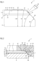
Figure 1 shows an exemplary embodiment of a semiconductor device in sectional view; -
Figure 2 shows a further exemplary embodiment of a semiconductor device in sectional view; -
Figure 3A shows simulation results of the electric field for a semiconductor device according to an embodiment of the semiconductor device described herein; -
Figure 3B shows simulation results of the electric field for a reference semiconductor device; -
Figure 4 shows measurements of the blocking voltage Vdc for different semiconductor devices. - The elements illustrated in the figures and their size relationships among one another are not necessarily true to scale. Rather, individual elements or layer thicknesses may be represented with an exaggerated size for the sake of better representability and/or for the sake of better understanding. An exemplary embodiment of a
semiconductor device 1 is illustrated inFigure 1 in cross-sectional view. In this exemplary embodiment, thesemiconductor device 1 is embodied as a semiconductor device having two blocking pn junctions for forward and reverse blocking. However, the invention may also be used for semiconductor devices having more than two pn junctions. - Metal electrodes of the
semiconductor device 1 such as cathode, anode and gate electrode are not explicitly shown in the Figures. - The
semiconductor device 1 comprises asemiconductor body 2 that extends in a vertical direction between a firstmain surface 21 and a secondmain surface 22. Thesemiconductor body 2 comprises a plurality of differently doped partial regions. For the sake of simplicity only, afirst semiconductor layer 31, asecond semiconductor layer 32 and athird semiconductor layer 33 are shown. However, the semiconductor body may comprise more than three semiconductor layers or differently doped semiconductor regions. - The
semiconductor body 2 is arranged on acarrier 6. For instance thesemiconductor body 2 is fixed to thecarrier 6 by means of a connecting layer such as an adhesive or a solder (not explicitly shown in the figures). - For example the
carrier 6 comprises molybdenum or consists of molybdenum. However, other materials may be used for thecarrier 6 as well. - A
first pn junction 41 is formed between thefirst semiconductor layer 31 and thesecond semiconductor layer 32. For instance, thesecond semiconductor layer 32 is n-doped and thefirst semiconductor layer 31 and thethird semiconductor layer 33 are p-doped or vice versa. For instance thesemiconductor body 2 is configured as a semiconductor disk. The semiconductor disk is a silicon wafer, for example. However, other semiconductor materials such as silicon carbide or gallium nitride may also be used. - The
first pn junction 41 and thesecond pn junction 42 extend in lateral direction betweenside surfaces 5 that laterally delimit thefirst pn junction 41 and thesecond pn junction 42. Theside surface 5 comprises a firstpartial region 51, a secondpartial region 52 and a thirdpartial region 53. These partial regions differ from one another with respect to the angle of theside surface 5 in the respective region with respect to thefirst pn junction 41. - The
first pn junction 41 is laterally delimited by the firstpartial region 51. Thus, the firstpartial region 51 laterally delimits in regions thefirst semiconductor layer 31 and thesecond semiconductor layer 32. The secondpartial region 52 extends between the first partial region and the firstmain surface 21. The secondpartial region 52 is spaced apart from thefirst pn junction 41 in vertical direction. - The first angle α (cf.
Figure 2 ) is between 5° and 20° inclusive, for instance, for example 10° or 14°. The second angle β is between 0.8° and 5° inclusive, for instance, for example 1°. - The
first semiconductor layer 31 is more heavily doped than thesecond semiconductor layer 32 so that the cross-section of the semiconductor device decreases towards the more heavily doped layer. Consequently, the firstpartial region 51 together with the secondpartial region 52 forms a negative bevel design for thefirst pn junction 41. - The
third semiconductor layer 33 is more heavily doped than thesecond semiconductor layer 32 so that the thirdpartial region 53 forms a positive bevel design for thesecond pn junction 42. The third angle γ between the thirdpartial region 53 and thefirst pn junction 41 is between 20° and 60° inclusive. - Within the first
partial region 51, the secondpartial region 52 and the thirdpartial region 53, the angle of theside surface 5 with respect to thefirst pn junction 41 is constant. Partial regions of theside surface 5 being flat in a cross-sectional view may be formed efficiently using a mechanical ablation method. Such a method may result intraces 55 characteristic of the respective ablation method, such as a grinding method. The traces are schematically shown in an enlarged section of theside surface 5 inFigure 1 . - The grinding may be performed such that also material of the
carrier 6 is removed so that at least part of aside surface 60 of thecarrier 6 has the same angle with respect to thefirst pn junction 41 as the thirdpartial region 53. Other ablation methods may also be used, for example a laser ablation method, resulting in characteristic traces 55. -
Figure 2 illustrates an exemplary embodiment of asemiconductor device 1 wherein the structure of the semiconductor body is shown in more detail. The description ofFigure 1 applies toFigure 2 as well unless otherwise indicated. - When seen from the first
main surface 21 towards the secondmain surface 22, thesemiconductor body 2 comprises afourth semiconductor layer 34 acting as an n+ layer, thefirst semiconductor layer 31 as p-layer, thesecond semiconductor layer 32 as n- layer, thethird semiconductor layer 33 as p-layer and afifth semiconductor layer 35 as a p+ layer. - Between the
fourth semiconductor layer 34 and the first semiconductor layer a further pn junction is formed. This further pn junction, however, does not extend to theside surface 5 in lateral direction. - The above layer structure may be used for a PCT thyristor, for instance. However, the layer structure may be modified within wide limits depending on the application of the
semiconductor device 1. - The first
main surface 21 represents a cathode side and the secondmain surface 22 an anode side of thesemiconductor body 2, for instance. - The first
partial region 51 is used to extend the shallow bevel region formed by the secondpartial region 52 through the deeply diffused cathode sidefirst pn junction 41. - The
side surface 5 of thesemiconductor body 2 is surrounded by an insulator 7, such as rubber, in order to protect the otherwise exposed first andsecond pn junctions side surface 5. - When seen along the vertical direction, a lateral extent w1 of the first
partial region 51 is smaller than a lateral extent w2 of the second partial region. - For example the lateral extent w1 amounts to 1 mm and the lateral extent w2 of the second
partial region 52 amounts to 2.1 mm for a semiconductor body with a thickness (i.e. extent in vertical direction) of 1.42 mm for a thyristor configured for a rated reverse blocking voltage of 8.5 kV. -
Figure 3A illustrates results of electrical simulations of the electrical field for a semiconductor device as described in connection withFigure 2 at a voltage of 7 kV applied in reverse direction. The simulation is based on a device with a first angle α of 10°. - For comparison
Figure 3B shows simulation results for a reference structure without a first partial region between the secondpartial region 52 and the thirdpartial region 53. -
Figure 3B illustrates that a punch through of the electrical field occurs at a voltage of 7 kV caused by the upturning of the electrical field near the transition to the positive bevel, i.e. between the two different partial regions of theside surface 5. - The simulation results shown in
Figure 3A , in contrast, confirm that high blocking capabilities can be obtained using the described configuration of theside surface 5 of thesemiconductor body 2 as a punch through can be avoided. - This has also been confirmed experimentally as shown by means of the experimental results illustrated in
Figure 4 . For the measurements, samples are used having different values w1 for the lateral extent of the first partial 51 wherein a value of 0 mm corresponds to a conventional device with only two different bevels. In each case, the first angle α amounts to 14°. - At 25°C the DC blocking voltage is significantly increased for the samples having a bevel length of 1 mm or 1.6 mm and an angle of 14° compared to the reference sample with w1 = 0 mm. Consequently, the proposed design of the
surface 5 of the semiconductor body allows to obtain asemiconductor device 1 such as a thyristor with high blocking voltage characteristics via a modified side surface of the semiconductor body. Thus, it is not necessary to increase the width of the n-base (the second semiconductor layer) of the thyristor until the punch through voltage is moved above the device maximum rated voltage. This solution would have the drawback that an increased thickness of the n-base would reduce the performance of the thyristor. -
- 1
- semiconductor device
- 2
- semiconductor body
- 21
- first main surface
- 22
- second main surface
- 31
- first semiconductor layer
- 32
- second semiconductor layer
- 33
- third semiconductor layer
- 34
- forth semiconductor layer
- 35
- fifth semiconductor layer
- 41
- first pn junction
- 42
- second pn junction
- 5
- side surface
- 51
- first partial region
- 52
- second partial region
- 53
- third partial region
- 55
- traces
- 6
- carrier
- 60
- side surface of carrier
- 7
- insulator
- α
- first angle
- β
- second angle
- γ
- third angle
- w1
- lateral extent of first partial region
- w2
- lateral extent of second partial region
Claims (9)
- A semiconductor device (1) with a semiconductor body (2), the semiconductor body (2) extending in a vertical direction between a first main surface (21) and a second main surface (22) opposite the first main surface (21), wherein- the semiconductor body (2) comprises a first semiconductor layer (31) of a first conductivity type and a second semiconductor layer (32) of a second conductivity type different from the first conductivity type thereby forming a first pn junction (41);- the first semiconductor layer (31) is more heavily doped than the second semiconductor layer (32);- a side surface (5) of the semiconductor body (2) extending between the first main surface (21) and the second main surface (22) delimits the semiconductor body (2) in a lateral direction;- the side surface (5) of the semiconductor body (2) comprises a first partial region (51) and a second partial region (52);- the first partial region (51) and the second partial region (52) delimit the first semiconductor layer (31) in regions;- the first partial region (51) delimits the first pn junction (41) in the lateral direction;- the second partial region (52) is spaced apart from the first pn junction (41) in the vertical direction; and- the first partial region (51) is arranged at a first angle (α) and the second partial region (52) is arranged at a second angle (β) with respect to the first pn junction (41) wherein the first angle (α) is larger than the second angle (β);- the side surface (5) comprises a third partial region (53), the first partial region (51) being arranged between the second partial region (52) and the third partial region (53), the third partial region (53) directly adjoining the first partial region (51);- the semiconductor body (2) further comprises a second pn junction (42), the third partial region (53) delimiting the second pn junction (42) in the lateral direction; and- the third partial region (53) is arranged at a third angle (γ) with respect to the first pn junction (41), wherein the third angle (γ) is larger than the first angle (α); and- the third angle (γ) is between 20° and 60° inclusive; andthe first angle (α) is constant within the first partial region (51), the second angle (β) is constant within the second partial region (52) and the third angle (γ) is constant within the third partial region (53).
- The semiconductor device (1) according to claim 1,
wherein the first angle (α) is between 5° and 20° inclusive. - The semiconductor device according to claim 1 or 2,
wherein the second angle (β) is between 0.8° and 5° inclusive. - The semiconductor device (1) according to any of the preceding claims,
wherein a lateral extent (w1) of the first partial region (51) is smaller than a lateral extent (w2) of the second partial (52) region when seen along the vertical direction. - The semiconductor device (1) according to any of the preceding claims,
wherein the first partial region (51) and the second partial region (52) exhibit traces (55) of a mechanical ablation method. - The semiconductor device (1) according to any of claims 1 to 4,
wherein the first partial region (51) and the second partial region (52) exhibit traces (55) of a laser ablation method. - The semiconductor device (1) according to any of the preceding claims,
wherein the second pn junction (42) is formed between the second semiconductor layer (32) and a third semiconductor layer (33) of the first conductivity type. - The semiconductor device (1) according to any of the preceding claims,
wherein the semiconductor device (1) is a thyristor. - The semiconductor device (1) according to claim 8,
wherein the thyristor has a positive-negative bevel design, wherein the negative bevel comprises the first and second partial region.
Priority Applications (5)
| Application Number | Priority Date | Filing Date | Title |
|---|---|---|---|
| EP20210372.7A EP4006990B1 (en) | 2020-11-27 | 2020-11-27 | Semiconductor device with a side surface having different partial regions |
| JP2023532389A JP7432100B2 (en) | 2020-11-27 | 2021-11-16 | Semiconductor device with side surfaces having different partial regions |
| CN202180079853.7A CN116569341B (en) | 2020-11-27 | 2021-11-16 | Semiconductor device with side surfaces having different local areas |
| PCT/EP2021/081856 WO2022112059A1 (en) | 2020-11-27 | 2021-11-16 | Semiconductor device with a side surface having different partial regions |
| US18/038,845 US12513949B2 (en) | 2020-11-27 | 2021-11-16 | Semiconductor device with a side surface having different partial regions |
Applications Claiming Priority (1)
| Application Number | Priority Date | Filing Date | Title |
|---|---|---|---|
| EP20210372.7A EP4006990B1 (en) | 2020-11-27 | 2020-11-27 | Semiconductor device with a side surface having different partial regions |
Publications (2)
| Publication Number | Publication Date |
|---|---|
| EP4006990A1 EP4006990A1 (en) | 2022-06-01 |
| EP4006990B1 true EP4006990B1 (en) | 2023-04-05 |
Family
ID=73642707
Family Applications (1)
| Application Number | Title | Priority Date | Filing Date |
|---|---|---|---|
| EP20210372.7A Active EP4006990B1 (en) | 2020-11-27 | 2020-11-27 | Semiconductor device with a side surface having different partial regions |
Country Status (5)
| Country | Link |
|---|---|
| US (1) | US12513949B2 (en) |
| EP (1) | EP4006990B1 (en) |
| JP (1) | JP7432100B2 (en) |
| CN (1) | CN116569341B (en) |
| WO (1) | WO2022112059A1 (en) |
Family Cites Families (25)
| Publication number | Priority date | Publication date | Assignee | Title |
|---|---|---|---|---|
| NL280641A (en) | 1961-07-07 | |||
| GB1052661A (en) | 1963-01-30 | 1900-01-01 | ||
| US3575644A (en) | 1963-01-30 | 1971-04-20 | Gen Electric | Semiconductor device with double positive bevel |
| US3255055A (en) | 1963-03-20 | 1966-06-07 | Hoffman Electronics Corp | Semiconductor device |
| NL6603372A (en) | 1965-03-25 | 1966-09-26 | ||
| US3579060A (en) * | 1969-03-21 | 1971-05-18 | Gen Electric | Thyristor with improved current and voltage handling characteristics |
| DE7328984U (en) * | 1973-07-06 | 1975-05-15 | Bbc Ag Brown Boveri & Cie | POWER SEMICONDUCTOR COMPONENT |
| JPS54163883U (en) * | 1978-05-09 | 1979-11-16 | ||
| JPS54163883A (en) | 1978-06-13 | 1979-12-26 | Mitsubishi Chem Ind | Improvement of yeast variety |
| JPS60224268A (en) * | 1984-04-20 | 1985-11-08 | Meidensha Electric Mfg Co Ltd | Power semiconductor devices |
| JPS6279667A (en) * | 1985-10-03 | 1987-04-13 | Mitsubishi Electric Corp | Semiconductor device |
| JP2603083B2 (en) * | 1987-10-02 | 1997-04-23 | 財団法人半導体研究振興会 | High voltage semiconductor device |
| JP2651678B2 (en) * | 1987-10-02 | 1997-09-10 | 財団法人半導体研究振興会 | High breakdown voltage semiconductor element and method of manufacturing the same |
| EP0532941B1 (en) * | 1991-09-20 | 1995-08-09 | eupec Europäische Gesellschaft für Leistungshalbleiter mbH & Co. KG | Thyristor with edge structure |
| JPH08242009A (en) * | 1994-12-02 | 1996-09-17 | Eurec Europ G Fur Leistungshalbleiter Mbh & Co Kg | Power semiconductor devices |
| DE69626299T2 (en) | 1996-09-24 | 2003-12-11 | Mitsubishi Denki K.K., Tokio/Tokyo | SEMICONDUCTOR ARRANGEMENT AND PRODUCTION METHOD |
| DE10250608B4 (en) | 2002-10-30 | 2005-09-29 | eupec Europäische Gesellschaft für Leistungshalbleiter mbH | Thyristor device with improved blocking behavior in the reverse direction |
| US7205583B1 (en) | 2005-12-22 | 2007-04-17 | Semiconductor Components Industries, L.L.C. | Thyristor and method of manufacture |
| JP6026418B2 (en) | 2010-09-27 | 2016-11-16 | アーベーベー・テヒノロギー・アーゲー | Bipolar non-punch-through power semiconductor device |
| EP2447988B1 (en) | 2010-11-02 | 2015-05-06 | GE Energy Power Conversion Technology Limited | Power electronic device with edge passivation |
| US20140151841A1 (en) * | 2012-12-01 | 2014-06-05 | North Carolina State University | Semiconductor devices having a positive-bevel termination or a negative-bevel termination and their manufacture |
| JP6742894B2 (en) | 2016-06-09 | 2020-08-19 | 株式会社日立製作所 | Data prediction system and data prediction method |
| DE102016124670B4 (en) | 2016-12-16 | 2020-01-23 | Semikron Elektronik Gmbh & Co. Kg | Thyristor with a semiconductor body |
| WO2019158594A1 (en) | 2018-02-13 | 2019-08-22 | Abb Schweiz Ag | Bidirectional thyristor device |
| JP2025163883A (en) | 2024-04-18 | 2025-10-30 | 株式会社デンソーテン | Vehicle control device, vehicle control method, and vehicle |
-
2020
- 2020-11-27 EP EP20210372.7A patent/EP4006990B1/en active Active
-
2021
- 2021-11-16 CN CN202180079853.7A patent/CN116569341B/en active Active
- 2021-11-16 US US18/038,845 patent/US12513949B2/en active Active
- 2021-11-16 WO PCT/EP2021/081856 patent/WO2022112059A1/en not_active Ceased
- 2021-11-16 JP JP2023532389A patent/JP7432100B2/en active Active
Also Published As
| Publication number | Publication date |
|---|---|
| EP4006990A1 (en) | 2022-06-01 |
| US12513949B2 (en) | 2025-12-30 |
| CN116569341B (en) | 2024-05-14 |
| CN116569341A (en) | 2023-08-08 |
| US20240021672A1 (en) | 2024-01-18 |
| JP2023545217A (en) | 2023-10-26 |
| JP7432100B2 (en) | 2024-02-16 |
| WO2022112059A1 (en) | 2022-06-02 |
Similar Documents
| Publication | Publication Date | Title |
|---|---|---|
| JP7724284B2 (en) | Trench-type power devices with improved reliability and continuity | |
| US6104062A (en) | Semiconductor device having reduced effective substrate resistivity and associated methods | |
| US10256314B2 (en) | Semiconductor device | |
| CN101221989B (en) | SiC Schottky barrier semiconductor device | |
| CN106531813B (en) | semiconductor device | |
| US9337186B2 (en) | Semiconductor device and a method for manufacturing a semiconductor device having a semi-insulating region | |
| EP3353814B1 (en) | Area efficient floating field ring termination | |
| CN103872099B (en) | Semiconductor Device with Step-Shaped Edge Termination, and Method for Manufacturing a Semiconductor Device | |
| CN108292669B (en) | Off-mode power semiconductor device and method of manufacturing the same | |
| CN102694014A (en) | Semiconductor device and method for manufacturing same | |
| US20150048489A1 (en) | Edge termination technique for high voltage power devices | |
| JP6337217B1 (en) | Power semiconductor device having a thick upper metal design and method of manufacturing the power semiconductor device | |
| EP3154091A1 (en) | Reverse-conducting semiconductor device | |
| EP2960941B1 (en) | Reverse-conducting power semiconductor device | |
| US20150255290A1 (en) | Method for manufacturing semiconductor device | |
| EP4439633A1 (en) | Power semiconductor device and method for producing a power semiconductor device | |
| WO1999052152A1 (en) | Semiconductor device and power converter | |
| US12513949B2 (en) | Semiconductor device with a side surface having different partial regions | |
| JP2005223349A (en) | High voltage semiconductor device and power converter using the same | |
| JP2015510272A (en) | SiC device with high blocking voltage, terminated by negative bevel | |
| US20070042549A1 (en) | Semiconductor device having reduced effective substrate resistivity and associated methods | |
| KR102170068B1 (en) | Bipolar non-punch-through power semiconductor device | |
| JP2018201050A (en) | Semiconductor device | |
| US20260032973A1 (en) | Gate trench power semiconductor devices having shallow trench shields and deep support shields | |
| CN121986570A (en) | Gate trench power semiconductor devices with shaped deep support shields that reduce cell pitch and on-state resistance |
Legal Events
| Date | Code | Title | Description |
|---|---|---|---|
| PUAI | Public reference made under article 153(3) epc to a published international application that has entered the european phase |
Free format text: ORIGINAL CODE: 0009012 |
|
| STAA | Information on the status of an ep patent application or granted ep patent |
Free format text: STATUS: THE APPLICATION HAS BEEN PUBLISHED |
|
| AK | Designated contracting states |
Kind code of ref document: A1 Designated state(s): AL AT BE BG CH CY CZ DE DK EE ES FI FR GB GR HR HU IE IS IT LI LT LU LV MC MK MT NL NO PL PT RO RS SE SI SK SM TR |
|
| RIN1 | Information on inventor provided before grant (corrected) |
Inventor name: JAGODA, DOBRZYNSKA Inventor name: AKURATI, KRANTHI KUMAR Inventor name: COMMIN, PAUL |
|
| STAA | Information on the status of an ep patent application or granted ep patent |
Free format text: STATUS: REQUEST FOR EXAMINATION WAS MADE |
|
| 17P | Request for examination filed |
Effective date: 20220726 |
|
| RBV | Designated contracting states (corrected) |
Designated state(s): AL AT BE BG CH CY CZ DE DK EE ES FI FR GB GR HR HU IE IS IT LI LT LU LV MC MK MT NL NO PL PT RO RS SE SI SK SM TR |
|
| GRAP | Despatch of communication of intention to grant a patent |
Free format text: ORIGINAL CODE: EPIDOSNIGR1 |
|
| STAA | Information on the status of an ep patent application or granted ep patent |
Free format text: STATUS: GRANT OF PATENT IS INTENDED |
|
| INTG | Intention to grant announced |
Effective date: 20221201 |
|
| GRAS | Grant fee paid |
Free format text: ORIGINAL CODE: EPIDOSNIGR3 |
|
| GRAA | (expected) grant |
Free format text: ORIGINAL CODE: 0009210 |
|
| STAA | Information on the status of an ep patent application or granted ep patent |
Free format text: STATUS: THE PATENT HAS BEEN GRANTED |
|
| AK | Designated contracting states |
Kind code of ref document: B1 Designated state(s): AL AT BE BG CH CY CZ DE DK EE ES FI FR GB GR HR HU IE IS IT LI LT LU LV MC MK MT NL NO PL PT RO RS SE SI SK SM TR |
|
| REG | Reference to a national code |
Ref country code: GB Ref legal event code: FG4D |
|
| REG | Reference to a national code |
Ref country code: DE Ref legal event code: R096 Ref document number: 602020009437 Country of ref document: DE |
|
| REG | Reference to a national code |
Ref country code: CH Ref legal event code: EP |
|
| REG | Reference to a national code |
Ref country code: AT Ref legal event code: REF Ref document number: 1558907 Country of ref document: AT Kind code of ref document: T Effective date: 20230415 |
|
| REG | Reference to a national code |
Ref country code: IE Ref legal event code: FG4D |
|
| P01 | Opt-out of the competence of the unified patent court (upc) registered |
Effective date: 20230527 |
|
| REG | Reference to a national code |
Ref country code: LT Ref legal event code: MG9D |
|
| REG | Reference to a national code |
Ref country code: NL Ref legal event code: MP Effective date: 20230405 |
|
| REG | Reference to a national code |
Ref country code: AT Ref legal event code: MK05 Ref document number: 1558907 Country of ref document: AT Kind code of ref document: T Effective date: 20230405 |
|
| PG25 | Lapsed in a contracting state [announced via postgrant information from national office to epo] |
Ref country code: NL Free format text: LAPSE BECAUSE OF FAILURE TO SUBMIT A TRANSLATION OF THE DESCRIPTION OR TO PAY THE FEE WITHIN THE PRESCRIBED TIME-LIMIT Effective date: 20230405 |
|
| PG25 | Lapsed in a contracting state [announced via postgrant information from national office to epo] |
Ref country code: SE Free format text: LAPSE BECAUSE OF FAILURE TO SUBMIT A TRANSLATION OF THE DESCRIPTION OR TO PAY THE FEE WITHIN THE PRESCRIBED TIME-LIMIT Effective date: 20230405 Ref country code: PT Free format text: LAPSE BECAUSE OF FAILURE TO SUBMIT A TRANSLATION OF THE DESCRIPTION OR TO PAY THE FEE WITHIN THE PRESCRIBED TIME-LIMIT Effective date: 20230807 Ref country code: NO Free format text: LAPSE BECAUSE OF FAILURE TO SUBMIT A TRANSLATION OF THE DESCRIPTION OR TO PAY THE FEE WITHIN THE PRESCRIBED TIME-LIMIT Effective date: 20230705 Ref country code: ES Free format text: LAPSE BECAUSE OF FAILURE TO SUBMIT A TRANSLATION OF THE DESCRIPTION OR TO PAY THE FEE WITHIN THE PRESCRIBED TIME-LIMIT Effective date: 20230405 Ref country code: AT Free format text: LAPSE BECAUSE OF FAILURE TO SUBMIT A TRANSLATION OF THE DESCRIPTION OR TO PAY THE FEE WITHIN THE PRESCRIBED TIME-LIMIT Effective date: 20230405 |
|
| PG25 | Lapsed in a contracting state [announced via postgrant information from national office to epo] |
Ref country code: RS Free format text: LAPSE BECAUSE OF FAILURE TO SUBMIT A TRANSLATION OF THE DESCRIPTION OR TO PAY THE FEE WITHIN THE PRESCRIBED TIME-LIMIT Effective date: 20230405 Ref country code: PL Free format text: LAPSE BECAUSE OF FAILURE TO SUBMIT A TRANSLATION OF THE DESCRIPTION OR TO PAY THE FEE WITHIN THE PRESCRIBED TIME-LIMIT Effective date: 20230405 Ref country code: LV Free format text: LAPSE BECAUSE OF FAILURE TO SUBMIT A TRANSLATION OF THE DESCRIPTION OR TO PAY THE FEE WITHIN THE PRESCRIBED TIME-LIMIT Effective date: 20230405 Ref country code: LT Free format text: LAPSE BECAUSE OF FAILURE TO SUBMIT A TRANSLATION OF THE DESCRIPTION OR TO PAY THE FEE WITHIN THE PRESCRIBED TIME-LIMIT Effective date: 20230405 Ref country code: IS Free format text: LAPSE BECAUSE OF FAILURE TO SUBMIT A TRANSLATION OF THE DESCRIPTION OR TO PAY THE FEE WITHIN THE PRESCRIBED TIME-LIMIT Effective date: 20230805 Ref country code: HR Free format text: LAPSE BECAUSE OF FAILURE TO SUBMIT A TRANSLATION OF THE DESCRIPTION OR TO PAY THE FEE WITHIN THE PRESCRIBED TIME-LIMIT Effective date: 20230405 Ref country code: GR Free format text: LAPSE BECAUSE OF FAILURE TO SUBMIT A TRANSLATION OF THE DESCRIPTION OR TO PAY THE FEE WITHIN THE PRESCRIBED TIME-LIMIT Effective date: 20230706 Ref country code: AL Free format text: LAPSE BECAUSE OF FAILURE TO SUBMIT A TRANSLATION OF THE DESCRIPTION OR TO PAY THE FEE WITHIN THE PRESCRIBED TIME-LIMIT Effective date: 20230405 |
|
| RAP2 | Party data changed (patent owner data changed or rights of a patent transferred) |
Owner name: HITACHI ENERGY LTD |
|
| PG25 | Lapsed in a contracting state [announced via postgrant information from national office to epo] |
Ref country code: FI Free format text: LAPSE BECAUSE OF FAILURE TO SUBMIT A TRANSLATION OF THE DESCRIPTION OR TO PAY THE FEE WITHIN THE PRESCRIBED TIME-LIMIT Effective date: 20230405 |
|
| REG | Reference to a national code |
Ref country code: DE Ref legal event code: R097 Ref document number: 602020009437 Country of ref document: DE |
|
| PG25 | Lapsed in a contracting state [announced via postgrant information from national office to epo] |
Ref country code: SK Free format text: LAPSE BECAUSE OF FAILURE TO SUBMIT A TRANSLATION OF THE DESCRIPTION OR TO PAY THE FEE WITHIN THE PRESCRIBED TIME-LIMIT Effective date: 20230405 |
|
| PG25 | Lapsed in a contracting state [announced via postgrant information from national office to epo] |
Ref country code: SM Free format text: LAPSE BECAUSE OF FAILURE TO SUBMIT A TRANSLATION OF THE DESCRIPTION OR TO PAY THE FEE WITHIN THE PRESCRIBED TIME-LIMIT Effective date: 20230405 Ref country code: SK Free format text: LAPSE BECAUSE OF FAILURE TO SUBMIT A TRANSLATION OF THE DESCRIPTION OR TO PAY THE FEE WITHIN THE PRESCRIBED TIME-LIMIT Effective date: 20230405 Ref country code: RO Free format text: LAPSE BECAUSE OF FAILURE TO SUBMIT A TRANSLATION OF THE DESCRIPTION OR TO PAY THE FEE WITHIN THE PRESCRIBED TIME-LIMIT Effective date: 20230405 Ref country code: EE Free format text: LAPSE BECAUSE OF FAILURE TO SUBMIT A TRANSLATION OF THE DESCRIPTION OR TO PAY THE FEE WITHIN THE PRESCRIBED TIME-LIMIT Effective date: 20230405 Ref country code: DK Free format text: LAPSE BECAUSE OF FAILURE TO SUBMIT A TRANSLATION OF THE DESCRIPTION OR TO PAY THE FEE WITHIN THE PRESCRIBED TIME-LIMIT Effective date: 20230405 Ref country code: CZ Free format text: LAPSE BECAUSE OF FAILURE TO SUBMIT A TRANSLATION OF THE DESCRIPTION OR TO PAY THE FEE WITHIN THE PRESCRIBED TIME-LIMIT Effective date: 20230405 |
|
| PLBE | No opposition filed within time limit |
Free format text: ORIGINAL CODE: 0009261 |
|
| STAA | Information on the status of an ep patent application or granted ep patent |
Free format text: STATUS: NO OPPOSITION FILED WITHIN TIME LIMIT |
|
| 26N | No opposition filed |
Effective date: 20240108 |
|
| REG | Reference to a national code |
Ref country code: DE Ref legal event code: R081 Ref document number: 602020009437 Country of ref document: DE Owner name: HITACHI ENERGY LTD, CH Free format text: FORMER OWNER: HITACHI ENERGY SWITZERLAND AG, BADEN, CH |
|
| PG25 | Lapsed in a contracting state [announced via postgrant information from national office to epo] |
Ref country code: SI Free format text: LAPSE BECAUSE OF FAILURE TO SUBMIT A TRANSLATION OF THE DESCRIPTION OR TO PAY THE FEE WITHIN THE PRESCRIBED TIME-LIMIT Effective date: 20230405 |
|
| PG25 | Lapsed in a contracting state [announced via postgrant information from national office to epo] |
Ref country code: SI Free format text: LAPSE BECAUSE OF FAILURE TO SUBMIT A TRANSLATION OF THE DESCRIPTION OR TO PAY THE FEE WITHIN THE PRESCRIBED TIME-LIMIT Effective date: 20230405 Ref country code: IT Free format text: LAPSE BECAUSE OF FAILURE TO SUBMIT A TRANSLATION OF THE DESCRIPTION OR TO PAY THE FEE WITHIN THE PRESCRIBED TIME-LIMIT Effective date: 20230405 |
|
| REG | Reference to a national code |
Ref country code: CH Ref legal event code: PL |
|
| PG25 | Lapsed in a contracting state [announced via postgrant information from national office to epo] |
Ref country code: MC Free format text: LAPSE BECAUSE OF FAILURE TO SUBMIT A TRANSLATION OF THE DESCRIPTION OR TO PAY THE FEE WITHIN THE PRESCRIBED TIME-LIMIT Effective date: 20230405 |
|
| PG25 | Lapsed in a contracting state [announced via postgrant information from national office to epo] |
Ref country code: LU Free format text: LAPSE BECAUSE OF NON-PAYMENT OF DUE FEES Effective date: 20231127 |
|
| PG25 | Lapsed in a contracting state [announced via postgrant information from national office to epo] |
Ref country code: CH Free format text: LAPSE BECAUSE OF NON-PAYMENT OF DUE FEES Effective date: 20231130 |
|
| PG25 | Lapsed in a contracting state [announced via postgrant information from national office to epo] |
Ref country code: MC Free format text: LAPSE BECAUSE OF FAILURE TO SUBMIT A TRANSLATION OF THE DESCRIPTION OR TO PAY THE FEE WITHIN THE PRESCRIBED TIME-LIMIT Effective date: 20230405 Ref country code: LU Free format text: LAPSE BECAUSE OF NON-PAYMENT OF DUE FEES Effective date: 20231127 Ref country code: CH Free format text: LAPSE BECAUSE OF NON-PAYMENT OF DUE FEES Effective date: 20231130 |
|
| REG | Reference to a national code |
Ref country code: BE Ref legal event code: MM Effective date: 20231130 |
|
| REG | Reference to a national code |
Ref country code: GB Ref legal event code: 732E Free format text: REGISTERED BETWEEN 20240718 AND 20240724 |
|
| REG | Reference to a national code |
Ref country code: IE Ref legal event code: MM4A |
|
| PG25 | Lapsed in a contracting state [announced via postgrant information from national office to epo] |
Ref country code: IE Free format text: LAPSE BECAUSE OF NON-PAYMENT OF DUE FEES Effective date: 20231127 |
|
| PG25 | Lapsed in a contracting state [announced via postgrant information from national office to epo] |
Ref country code: BE Free format text: LAPSE BECAUSE OF NON-PAYMENT OF DUE FEES Effective date: 20231130 |
|
| PG25 | Lapsed in a contracting state [announced via postgrant information from national office to epo] |
Ref country code: FR Free format text: LAPSE BECAUSE OF NON-PAYMENT OF DUE FEES Effective date: 20231130 |
|
| PG25 | Lapsed in a contracting state [announced via postgrant information from national office to epo] |
Ref country code: IE Free format text: LAPSE BECAUSE OF NON-PAYMENT OF DUE FEES Effective date: 20231127 Ref country code: FR Free format text: LAPSE BECAUSE OF NON-PAYMENT OF DUE FEES Effective date: 20231130 Ref country code: BE Free format text: LAPSE BECAUSE OF NON-PAYMENT OF DUE FEES Effective date: 20231130 |
|
| PG25 | Lapsed in a contracting state [announced via postgrant information from national office to epo] |
Ref country code: BG Free format text: LAPSE BECAUSE OF FAILURE TO SUBMIT A TRANSLATION OF THE DESCRIPTION OR TO PAY THE FEE WITHIN THE PRESCRIBED TIME-LIMIT Effective date: 20230405 |
|
| REG | Reference to a national code |
Ref country code: DE Ref legal event code: R079 Ref document number: 602020009437 Country of ref document: DE Free format text: PREVIOUS MAIN CLASS: H01L0029740000 Ipc: H10D0018000000 |
|
| PG25 | Lapsed in a contracting state [announced via postgrant information from national office to epo] |
Ref country code: BG Free format text: LAPSE BECAUSE OF FAILURE TO SUBMIT A TRANSLATION OF THE DESCRIPTION OR TO PAY THE FEE WITHIN THE PRESCRIBED TIME-LIMIT Effective date: 20230405 |
|
| REG | Reference to a national code |
Ref country code: DE Ref legal event code: R082 Ref document number: 602020009437 Country of ref document: DE Representative=s name: DENNEMEYER & ASSOCIATES RECHTSANWALTSGESELLSCH, DE |
|
| PG25 | Lapsed in a contracting state [announced via postgrant information from national office to epo] |
Ref country code: CY Free format text: LAPSE BECAUSE OF FAILURE TO SUBMIT A TRANSLATION OF THE DESCRIPTION OR TO PAY THE FEE WITHIN THE PRESCRIBED TIME-LIMIT; INVALID AB INITIO Effective date: 20201127 |
|
| PG25 | Lapsed in a contracting state [announced via postgrant information from national office to epo] |
Ref country code: HU Free format text: LAPSE BECAUSE OF FAILURE TO SUBMIT A TRANSLATION OF THE DESCRIPTION OR TO PAY THE FEE WITHIN THE PRESCRIBED TIME-LIMIT; INVALID AB INITIO Effective date: 20201127 |
|
| PG25 | Lapsed in a contracting state [announced via postgrant information from national office to epo] |
Ref country code: TR Free format text: LAPSE BECAUSE OF FAILURE TO SUBMIT A TRANSLATION OF THE DESCRIPTION OR TO PAY THE FEE WITHIN THE PRESCRIBED TIME-LIMIT Effective date: 20230405 |
|
| PGFP | Annual fee paid to national office [announced via postgrant information from national office to epo] |
Ref country code: DE Payment date: 20251119 Year of fee payment: 6 |
|
| PGFP | Annual fee paid to national office [announced via postgrant information from national office to epo] |
Ref country code: GB Payment date: 20251121 Year of fee payment: 6 |