EP4006631A1 - Arraysubstrat und flüssigkristallanzeigetafel - Google Patents
Arraysubstrat und flüssigkristallanzeigetafel Download PDFInfo
- Publication number
- EP4006631A1 EP4006631A1 EP19930173.0A EP19930173A EP4006631A1 EP 4006631 A1 EP4006631 A1 EP 4006631A1 EP 19930173 A EP19930173 A EP 19930173A EP 4006631 A1 EP4006631 A1 EP 4006631A1
- Authority
- EP
- European Patent Office
- Prior art keywords
- driving electrode
- line
- electrode line
- dummy
- electrode
- Prior art date
- Legal status (The legal status is an assumption and is not a legal conclusion. Google has not performed a legal analysis and makes no representation as to the accuracy of the status listed.)
- Granted
Links
Images



Classifications
-
- G—PHYSICS
- G02—OPTICS
- G02F—OPTICAL DEVICES OR ARRANGEMENTS FOR THE CONTROL OF LIGHT BY MODIFICATION OF THE OPTICAL PROPERTIES OF THE MEDIA OF THE ELEMENTS INVOLVED THEREIN; NON-LINEAR OPTICS; FREQUENCY-CHANGING OF LIGHT; OPTICAL LOGIC ELEMENTS; OPTICAL ANALOGUE/DIGITAL CONVERTERS
- G02F1/00—Devices or arrangements for the control of the intensity, colour, phase, polarisation or direction of light arriving from an independent light source, e.g. switching, gating or modulating; Non-linear optics
- G02F1/01—Devices or arrangements for the control of the intensity, colour, phase, polarisation or direction of light arriving from an independent light source, e.g. switching, gating or modulating; Non-linear optics for the control of the intensity, phase, polarisation or colour
- G02F1/13—Devices or arrangements for the control of the intensity, colour, phase, polarisation or direction of light arriving from an independent light source, e.g. switching, gating or modulating; Non-linear optics for the control of the intensity, phase, polarisation or colour based on liquid crystals, e.g. single liquid crystal display cells
- G02F1/133—Constructional arrangements; Operation of liquid crystal cells; Circuit arrangements
- G02F1/136—Liquid crystal cells structurally associated with a semi-conducting layer or substrate, e.g. cells forming part of an integrated circuit
- G02F1/1362—Active matrix addressed cells
- G02F1/136286—Wiring, e.g. gate line, drain line
-
- G—PHYSICS
- G02—OPTICS
- G02F—OPTICAL DEVICES OR ARRANGEMENTS FOR THE CONTROL OF LIGHT BY MODIFICATION OF THE OPTICAL PROPERTIES OF THE MEDIA OF THE ELEMENTS INVOLVED THEREIN; NON-LINEAR OPTICS; FREQUENCY-CHANGING OF LIGHT; OPTICAL LOGIC ELEMENTS; OPTICAL ANALOGUE/DIGITAL CONVERTERS
- G02F1/00—Devices or arrangements for the control of the intensity, colour, phase, polarisation or direction of light arriving from an independent light source, e.g. switching, gating or modulating; Non-linear optics
- G02F1/01—Devices or arrangements for the control of the intensity, colour, phase, polarisation or direction of light arriving from an independent light source, e.g. switching, gating or modulating; Non-linear optics for the control of the intensity, phase, polarisation or colour
- G02F1/13—Devices or arrangements for the control of the intensity, colour, phase, polarisation or direction of light arriving from an independent light source, e.g. switching, gating or modulating; Non-linear optics for the control of the intensity, phase, polarisation or colour based on liquid crystals, e.g. single liquid crystal display cells
- G02F1/133—Constructional arrangements; Operation of liquid crystal cells; Circuit arrangements
- G02F1/1333—Constructional arrangements; Manufacturing methods
- G02F1/13338—Input devices, e.g. touch panels
-
- G—PHYSICS
- G02—OPTICS
- G02F—OPTICAL DEVICES OR ARRANGEMENTS FOR THE CONTROL OF LIGHT BY MODIFICATION OF THE OPTICAL PROPERTIES OF THE MEDIA OF THE ELEMENTS INVOLVED THEREIN; NON-LINEAR OPTICS; FREQUENCY-CHANGING OF LIGHT; OPTICAL LOGIC ELEMENTS; OPTICAL ANALOGUE/DIGITAL CONVERTERS
- G02F1/00—Devices or arrangements for the control of the intensity, colour, phase, polarisation or direction of light arriving from an independent light source, e.g. switching, gating or modulating; Non-linear optics
- G02F1/01—Devices or arrangements for the control of the intensity, colour, phase, polarisation or direction of light arriving from an independent light source, e.g. switching, gating or modulating; Non-linear optics for the control of the intensity, phase, polarisation or colour
- G02F1/13—Devices or arrangements for the control of the intensity, colour, phase, polarisation or direction of light arriving from an independent light source, e.g. switching, gating or modulating; Non-linear optics for the control of the intensity, phase, polarisation or colour based on liquid crystals, e.g. single liquid crystal display cells
- G02F1/133—Constructional arrangements; Operation of liquid crystal cells; Circuit arrangements
- G02F1/1333—Constructional arrangements; Manufacturing methods
- G02F1/1343—Electrodes
- G02F1/134309—Electrodes characterised by their geometrical arrangement
-
- G—PHYSICS
- G06—COMPUTING OR CALCULATING; COUNTING
- G06F—ELECTRIC DIGITAL DATA PROCESSING
- G06F3/00—Input arrangements for transferring data to be processed into a form capable of being handled by the computer; Output arrangements for transferring data from processing unit to output unit, e.g. interface arrangements
- G06F3/01—Input arrangements or combined input and output arrangements for interaction between user and computer
- G06F3/03—Arrangements for converting the position or the displacement of a member into a coded form
- G06F3/041—Digitisers, e.g. for touch screens or touch pads, characterised by the transducing means
- G06F3/0412—Digitisers structurally integrated in a display
-
- G—PHYSICS
- G06—COMPUTING OR CALCULATING; COUNTING
- G06F—ELECTRIC DIGITAL DATA PROCESSING
- G06F3/00—Input arrangements for transferring data to be processed into a form capable of being handled by the computer; Output arrangements for transferring data from processing unit to output unit, e.g. interface arrangements
- G06F3/01—Input arrangements or combined input and output arrangements for interaction between user and computer
- G06F3/03—Arrangements for converting the position or the displacement of a member into a coded form
- G06F3/041—Digitisers, e.g. for touch screens or touch pads, characterised by the transducing means
- G06F3/044—Digitisers, e.g. for touch screens or touch pads, characterised by the transducing means by capacitive means
- G06F3/0443—Digitisers, e.g. for touch screens or touch pads, characterised by the transducing means by capacitive means using a single layer of sensing electrodes
-
- G—PHYSICS
- G06—COMPUTING OR CALCULATING; COUNTING
- G06F—ELECTRIC DIGITAL DATA PROCESSING
- G06F3/00—Input arrangements for transferring data to be processed into a form capable of being handled by the computer; Output arrangements for transferring data from processing unit to output unit, e.g. interface arrangements
- G06F3/01—Input arrangements or combined input and output arrangements for interaction between user and computer
- G06F3/03—Arrangements for converting the position or the displacement of a member into a coded form
- G06F3/041—Digitisers, e.g. for touch screens or touch pads, characterised by the transducing means
- G06F3/044—Digitisers, e.g. for touch screens or touch pads, characterised by the transducing means by capacitive means
- G06F3/0446—Digitisers, e.g. for touch screens or touch pads, characterised by the transducing means by capacitive means using a grid-like structure of electrodes in at least two directions, e.g. using row and column electrodes
Definitions
- the present disclosure relates to the technical field of display, and in particular, to an array substrate and a liquid crystal display.
- LCD displays have been widely used in the market. Due to their simpler and faster human-computer interaction, LCDs with touch control or touch functions have become more and more popular. In-cell touch display screens have the advantages of being light and thin, increased definition and low cost, and therefore, have been steadily and continuously growing in high-end display markets.
- the array substrate includes at least one driving electrode region and at least one sensing electrode region which are alternately arranged along a row direction and are disconnected from each other, each driving electrode region includes one first common electrode and each sensing electrode region includes one second common electrode respectively.
- At least one driving electrode line extends along the row direction and continuously passes through the driving electrode region and the sensing electrode region alternately arranged along the row direction.
- the first common electrode in the driving electrode region is connected to the driving electrode line through at least one first through hole, and the second common electrode in the sensing electrode region is disconnected from the driving electrode line.
- the sensing electrode region is formed therein with at least one second dummy driving electrode line parallel to the driving electrode line, and the second common electrode in the sensing electrode region is connected to the second dummy driving electrode line through at least one fifth through hole.
- a number of the fifth through holes is the same as a number of the first through holes.
- the driving electrode region is formed therein with at least one first dummy driving electrode line parallel to the driving electrode line.
- the array substrate includes a plurality of pixel units arranged in a plurality of rows and a plurality of columns. A plurality of adjacent rows of pixel units are disposed with one driving electrode line. Each pixel unit where the driving electrode line is not formed in the sensing electrode region is formed with one second dummy driving electrode line therein.
- each pixel unit where the driving electrode line is not formed in the driving electrode region is formed with one first dummy driving electrode line therein.
- the first dummy driving electrode line is disconnected from the second dummy driving electrode line.
- first common electrodes in driving electrode regions adjacent in a column direction are separated from each other.
- the second common electrodes in the sensing electrode regions are formed as one piece in the column direction.
- the first common electrode is disconnected from the adjacent second common electrode in the row direction.
- the first common electrode in each driving electrode regions is formed thereon with at least one transverse dummy sensing electrode line and at least one longitudinal dummy sensing electrode line.
- the at least one transverse dummy sensing electrode line is parallel to the driving electrode line in the row direction, and the at least one longitudinal dummy sensing electrode line is arranged in a column direction and connected to the at least one transverse dummy sensing electrode line.
- the second common electrode in each sensing electrode region is formed thereon with at least one transverse sensing electrode line and at least one longitudinal sensing electrode line, the at least one transverse sensing electrode line parallel to the driving electrode line in the row direction, and the at least one longitudinal sensing electrode line arranged in the column direction and connected to the at least one transverse sensing electrode line.
- the array substrate includes a plurality of pixel units arranged in a plurality of rows and columns.
- Each pixel unit in the driving electrode region is formed therein with one transverse dummy sensing electrode line. Every multiple adjacent columns of pixel units in the driving electrode region are disposed with one longitudinal dummy sensing electrode line.
- Each pixel unit in the sensing electrode region is formed therein with one transverse sensing electrode line. Every multiple adjacent columns of pixel units in the sensing electrode region are disposed with one longitudinal sensing electrode line.
- the first common electrode is connected to the driving electrode line through two first through holes in each driving electrode region
- the second common electrode is connected to the second dummy driving electrode line through two fifth through holes in each sensing electrode region.
- the two fifth through holes are respectively located in the second dummy driving electrode lines on two sides of the driving electrode line.
- the two second through holes are both located in the second dummy driving electrode line on one side of the driving electrode line.
- both the first and second dummy driving electrode lines are intermittent in the first and second common electrode regions.
- both the first and second dummy driving electrode lines are continuous in the driving electrode region and the sensing electrode region.
- both the first and second dummy driving electrode lines are intermittent or continuous in the driving electrode region and the sensing electrode region, and a size of the sensing electrode region in the row direction is smaller than a size of the driving electrode region in the row direction.
- the transverse and longitudinal dummy sensing electrode lines are on and in direct contact with the first common electrode in the driving electrode region, and the transverse and longitudinal sensing electrode lines are on and in direct contact with the second common electrode in the sensing electrode region.
- the array substrate includes a plurality of gate lines and a plurality of data lines.
- the driving electrode line is located on the same layer as the gate lines and parallel to the gate lines
- an orthographic projection of the driving electrode line on a base substrate of the array substrate overlaps an orthographic projection of the transverse dummy sensing electrode line in the same row as the driving electrode line on the base substrate
- the first dummy driving electrode line is located on the same layer as the gate lines and parallel to the gate lines
- an orthographic projection of the first dummy driving electrode line on the base substrate overlaps an orthographic projection of the transverse dummy sensing electrode line in the same row as the first dummy driving electrode line on the base substrate
- an orthographic projection of the longitudinal dummy sensing electrode line on the base substrate overlaps an orthographic projection of the data line on the base substrate.
- the array substrate includes a plurality of gate lines and a plurality of data lines.
- the driving electrode line is located on the same layer as the gate lines and parallel to the gate lines
- an orthographic projection of the driving electrode line on the base substrate overlaps an orthographic projection of the transverse sensing electrode line in the same row as the driving electrode line on the base substrate
- the second dummy driving electrode line is located on the same layer as the gate lines and parallel to the gate lines
- an orthographic projection of the second dummy driving electrode line on the base substrate overlaps an orthographic projection of the transverse sensing electrode line in the same row as the second dummy driving electrode line on the base substrate
- an orthographic projection of the longitudinal sensing electrode line on the base substrate overlaps an orthographic projection of the data line on the base substrate.
- the array substrate includes a plurality of pixel units arranged in a plurality of rows and a plurality of columns.
- a pixel unit having the driving electrode line in the driving electrode region includes: a base substrate; an active layer located on the base substrate; a gate insulating layer covering the active layer; a gate line and the driving electrode line located on the gate insulating layer; an interlayer insulating layer covering the gate line, the driving electrode line and the gate insulating layer; a data line, a drain and a first auxiliary electrode located on the interlayer insulating layer, with the data line connected to one side of the active layer through a second through hole, the drain connected to the other side of the active layer through a third through hole, and the first auxiliary electrode connected to the driving electrode line through a six through hole; a planarization layer covering the data line, the drain, the first auxiliary electrode and the interlayer insulating layer; the first common electrode located on the planarization layer, with the transverse and longitudinal dummy sensing electrode lines being on and
- the array substrate includes a plurality of pixel units arranged in a plurality of rows and a plurality of columns. At least one of the plurality of pixel units in the sensing electrode region and adjacent, in a column direction, to a pixel unit including the driving electrode line includes: a base substrate; an active layer located on the base substrate; a gate insulating layer covering the active layer; a gate line and the second dummy driving electrode line located on the gate insulating layer; an interlayer insulating layer covering the gate line, the second dummy driving electrode line and the gate insulating layer; a data line, a drain and a first auxiliary electrode which are located on the interlayer insulating layer, with the data line connected to one side of the active layer through a second through hole, the drain connected to the other side of the active layer through a third through hole, and the first auxiliary electrode connected to the second dummy driving electrode line through a seventh through hole; a planarization layer covering the data line, the drain, the first auxiliary electrode
- a touch liquid crystal display including above array substrate is provided.
- the array substrate of the display panel is provided with common electrodes, and at least a part of the common electrodes also function as touch electrodes. That is, such electrodes serve as the touch electrodes when a touch action is received, and serves as the common electrodes when no touch action is received.
- the common electrode region for providing a touch driving function is referred to as a driving electrode region
- the common electrode region for providing a touch sensing function is referred to as a sensing electrode region in the present disclosure.
- the common electrodes in the driving electrode regions are referred to as first common electrodes
- the common electrodes in the sensing electrode regions are referred to as second common electrodes.
- the first common electrodes and the electrode lines located on the first common electrodes in the driving electrode regions are referred to as driving electrodes
- the second common electrodes and the electrode lines located on the second common electrodes in the sensing electrode regions are referred to as sensing electrodes.
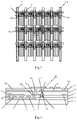
- a plurality of first common electrodes 81 and a plurality of second sensing electrodes 82 are alternately arranged on an array substrate in a row direction and are separated from each other. Adjacent first common electrodes 81 are separated from each other in a column direction, and the second common electrodes 82 are uninterrupted or continuous in the column direction. Accordingly, the array substrate is divided into a plurality of driving electrode regions 810 and a plurality of sensing electrode regions 820 alternately arranged in the row direction.
- Driving electrode lines 83 are disposed along the row direction, and continuously pass through the driving electrode regions 810 and the sensing electrode regions 820 alternately arranged along the row direction.
- Sensing electrode lines are disposed on the second common electrode 82 in the sensing electrode region 820, and include transverse sensing electrode lines 821 and longitudinal sensing electrode lines 822, which are connected to each other.
- dummy sensing electrode lines are disposed on the first common electrode 81 in the driving electrode region 810, and include transverse dummy sensing electrode lines 811 and longitudinal dummy sensing electrode lines 812, which are connected to each other.
- first dummy driving electrode lines 841 and second dummy driving electrode lines 842 are accordingly disposed in the driving electrode regions 810 and the sensing electrode regions 820 respectively.
- the driving electrode line 83, the first dummy driving electrode line 841, the second dummy driving electrode line 842 and gate line 4 are disposed on the same layer.
- the driving electrode line 83 is connected to the first common electrodes 81 through a through hole, and thus the distribution of the electric field of the array substrate changes due to the through hole. Therefore, the through hole is formed in the sensing electrode region 820 for connecting the second dummy driving electrode lines 842 with the second common electrodes 82, so as to ensure a more uniform electric field of the array substrate.
- the first common electrode 81, and the transverse dummy sensing electrode lines 811 and the longitudinal dummy sensing electrode lines 812 located on the first common electrode 81 are referred to as a driving electrode.
- the second common electrode 82, and the transverse sensing electrode lines 821 and the longitudinal sensing electrode lines 822 located on the second common electrode 82 are referred to as a sensing electrode.
- the longitudinal dummy sensing electrode line 812 and the transverse dummy sensing electrode line 811 are formed in the same layer as the longitudinal sensing electrode line 822 and the transverse sensing electrode line 821.
- the longitudinal dummy sensing electrode lines 812 and the transverse dummy sensing electrode lines 811 in the driving electrode region 810 are disconnected from the longitudinal sensing electrode lines 822 and the transverse sensing electrode lines 821 in the sensing electrode region 820.
- the longitudinal dummy sensing electrode lines 812 and the transverse dummy sensing electrode lines 811 in a driving electrode region 810 are disconnected from the longitudinal dummy sensing electrode lines 812 and the transverse dummy sensing electrode lines 811 in another driving electrode region 810 adjacent to the driving electrode region 810 along the column direction.
- the driving electrode lines 83 in the driving electrode regions 810 and the sensing electrode regions 820 are connected together in the row direction.
- the first dummy driving electrode lines 841 in the driving electrode region 810 are disconnected from the second dummy driving electrode lines 842 in the sensing electrode region 820.
- an array substrate includes a plurality of pixel units arranged in a plurality of rows and a plurality of columns.
- a plurality of data lines are respectively arranged between the plurality of columns of pixel units along a column direction, and a plurality of gate lines are respectively arranged between the plurality of rows of pixel units along a row direction.
- One driving electrode line is provided for a plurality of adjacent rows of pixel units.
- the driving electrode lines and the gate lines are located on the same layer and are parallel to one another, but an orthographic projection of the driving electrode line on a base substrate does not overlap an orthographic projection of the gate line on the base substrate.
- the row direction refers to a direction along which the gate lines extend
- the column direction refers to a direction along which the data lines extend.
- the sensing electrode region 820 is smaller than the driving electrode region 810 in size along the row direction, that is, the number of the pixel units in a sensing electrode region 820 along the row direction is less than that of the pixel units in the driving electrode region 810.
- One driving electrode line 83 is provided for a plurality of adjacent rows of pixel units.
- One second dummy driving electrode line 842 is disposed for each pixel unit in the sensing electrode region where the driving electrode line is not formed.
- One first dummy driving electrode line 841 is disposed for each pixel unit in the driving electrode regions 810 where the driving electrode line 83 is not formed. The first dummy driving electrode lines 841 are disconnected from the second dummy driving electrode line 842.
- One transverse dummy sensing electrode line 811 is disposed for each pixel unit in the driving electrode regions 810, and one longitudinal dummy sensing electrode line 812 is disposed for/associated with every multiple adjacent columns of pixel units in the driving electrode regions 810.
- the transverse dummy sensing electrode lines 811 are parallel to the driving electrode lines 83.
- the transverse dummy sensing electrode lines 811 of the pixel units adjacent to each other in the row direction may be connected together.
- the longitudinal dummy sensing electrode lines 812 disposed in the column direction connects the transverse dummy sensing electrode lines 811 of all rows. Multiple longitudinal dummy sensing electrode lines 812 are disposed along the column direction in each of the driving electrode region 810.
- an interval between the adjacent longitudinal dummy sensing electrode lines 812 in a driving electrode region 810 is the same as an interval between the adjacent longitudinal sensing electrode lines 822 in an adjacent sensing electrode region 820, so as to obtain a uniform electric field.
- the longitudinal dummy sensing electrode lines 812 in each driving electrode region 810 may be continuous in the column direction, but are disconnected from the longitudinal dummy sensing electrode lines 812 in another driving electrode region 810 adjacent to the driving electrode region in the column direction.
- One transverse sensing electrode line 821 is located in the pixel units in the sensing electrode regions 820, and each transverse sensing electrode line 821 is parallel to the driving electrode lines 83.
- a plurality of longitudinal sensing electrode lines 822 are disposed along the column direction in each sensing electrode regions 820 to connect the transverse sensing electrode lines 821, and every multiple adjacent columns of pixel units in each sensing electrode region 820 are provided with one corresponding longitudinal sensing electrode line 822.
- the longitudinal sensing electrode lines 822 of each column are continuous. In some embodiments, an interval between the adjacent longitudinal sensing electrode lines 822 in the sensing electrode regions 820 is the same as an interval between the adjacent longitudinal dummy sensing electrode lines 812 in the driving electrode regions 810, so as to obtain a uniform electric field.
- the first common electrode 81 is connected to the driving electrode line 83 through a first through hole 01 in a driving electrode region 810.
- the first through hole 01 includes a lower portion of first through hole 011 which penetrates through an interlayer insulating layer 5, and an upper portion of first through hole 012 which penetrates through a planarization layer 7.
- the driving electrode line 83 is located on a gate line layer of a pixel unit and is parallel to a gate line 4, an orthographic projection of the driving electrode line 83 on a base substrate 1 of the array substrate overlaps with an orthographic projection, on the base substrate 1, of a transverse dummy sensing electrode line 811 in the same row as the driving electrode line 83.
- the first dummy driving electrode line 841 is also located on the gate line layer of the pixel unit.
- An orthographic projection of the first dummy driving electrode line 841 on the base substrate 1 overlaps an orthographic projection, on the base substrate 1, of the transverse dummy sensing electrode line 811 in the same row as the first dummy driving electrode line 841.
- An orthographic projection of a longitudinal dummy sensing electrode line 812 on the base substrate overlaps an orthographic projection of a data line 6 on the base substrate 1.
- the driving electrode line 83 is disconnected from the second common electrode 82 in a sensing electrode region 820.
- the second dummy driving electrode line 842 is connected to the second common electrode 82 through a fifth through hole 05.
- the fifth through hole 05 includes a lower portion of fifth through hole 051 which penetrates through the interlayer insulating layer 5, and an upper portion of fifth through hole 052 which penetrates through the planarization layer 7.
- the driving electrode line 83 is located on the gate line layer of the pixel unit and is parallel to the gate line 4, an orthographic projection of the driving electrode line 83 on the base substrate 1 overlaps an orthographic projection, on the base substrate 1, of a transverse sensing electrode line 821 in the same row as the driving electrode line 83.
- the second dummy driving electrode line 842 is located on the gate line layer of the pixel unit, an orthographic projection of the second dummy driving electrode line 842 on the base substrate 1 overlaps an orthographic projection, on the base substrate 1, of the transverse sensing electrode line 821 in the same row as the second dummy driving electrode line 842.
- An orthographic projection of the longitudinal sensing electrode line 822 on the base substrate 1 overlaps an orthographic projection of the data line 6 on the base substrate 1.
- the sensing electrode region 820 and the adjacent driving electrode region 810 have similar circuit arrangement, so that the driving electrodes in the driving electrode regions 810 and the sensing electrodes in the sensing electrode regions 820 of the array substrate can generate similar electric fields, thereby enabling the array substrate to display more uniformly.
- the transverse dummy sensing electrode lines 811 and the longitudinal dummy sensing electrode lines 812 are correspondingly disposed on the common electrode in the driving electrode region.
- the first dummy driving electrode lines in the driving electrode regions and the second dummy driving electrode lines in the sensing electrode regions are disconnected from each other, and the first dummy driving electrode lines in the driving electrode regions that are adjacent along the column direction are disconnected from each other.
- the first dummy driving electrode lines in the driving electrode regions and the second dummy driving electrode lines in the sensing electrode regions are all in a floating state.
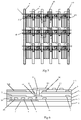
- the first dummy driving electrode lines in the driving electrode regions and the second dummy driving electrode lines in the sensing electrode regions may be continuous or intermittent. Referring to Fig. 2 , the first dummy driving electrode line in the driving electrode region or the second dummy driving electrode line in the sensing electrode region includes a plurality of segments.
- the first dummy driving electrode line in the driving electrode region and the second dummy driving electrode line in the sensing electrode region are intermittent.
- the first dummy driving electrode line in each driving electrode region and the second dummy driving electrode line in each sensing electrode region are equally divided into four segments respectively.
- Fig. 3 is a plan view of pixel structures in the driving electrode regions shown in Fig. 1 or Fig. 2
- Fig. 4 is a sectional view taken along AA' of Fig. 3
- a pixel electrode 10 is located above the first common electrode 81.
- the pixel electrode 10 is provided with a slit, and connected to a drain 60 of a thin film transistor of a pixel unit through a fourth through hole 04 penetrating through a first insulating layer 9 and the planarization layer 7.
- the first common electrode 81, and the transverse dummy sensing electrode line 811 and the longitudinal dummy sensing electrode line 812 which are located on the first common electrode 81 in the driving electrode region 810 serve as a driving electrode.
- the driving electrode line 83 is located on the gate line layer, the first common electrode 81 is connected to the driving electrode line 83 through the first through hole 01.
- the longitudinal dummy sensing electrode line 812 overlaps the data line 6 in a direction perpendicular to the base substrate 1
- the transverse dummy sensing electrode line 811 overlaps the driving electrode line 83 or the first dummy driving electrode line 841 in the direction perpendicular to the base substrate 1.
- Fig. 5 is a diagram of pixel structures in the sensing electrode regions shown in Fig. 1 or Fig. 2 .
- Fig. 6 is a sectional view taken along AA' of Fig. 5
- Fig. 7 is a sectional view taken along BB' of Fig. 5 .
- the second common electrode 82, and the longitudinal sensing electrode line 822 and the transverse sensing electrode 821 which are located on the second common electrode in the sensing electrode region serve as a sensing electrode.
- the longitudinal sensing electrode line 822 overlaps the data line 6 in the direction perpendicular to the base substrate 1, and the transverse sensing electrode line 821 overlaps the driving electrode line 83 or the second dummy driving electrode line 842 of the same row in the direction perpendicular to the base substrate 1.
- the driving electrode line 83 is disconnected from the second common electrode 82.
- the second common electrode 82 is connected to the second dummy driving electrode line 842 through the fifth through hole 05 in the sensing electrode region 820.
- a pixel unit including a driving electrode line includes: a base substrate 1; an active layer 2 located on the base substrate 1; a gate insulating layer 3 covering the active layer 2; a gate line 4 and a driving electrode line 83 located on the gate insulating layer 3; an interlayer insulating layer 5 covering the gate line 4, the driving electrode line 83, and the gate insulating layer 3; a data line 6, a drain 60 and a first auxiliary electrode 61 which are located on the interlayer insulating layer 5, with the data line 6 connected to a side of the active layer 2 through a second through hole 02, the drain 60 connected to the other side of the active layer through a third through hole 03, the first auxiliary electrode 61 connected to the driving electrode line 83 through a lower portion 011 of a first through hole 01, and the second through hole 02 and the third through hole 03 penetrating through the interlayer insulating layer 5 and the gate insulating layer 3;
- a pixel unit including a driving electrode line in a sensing electrode region 820 differs from the pixel unit including the driving electrode line in the driving electrode region in that a transverse sensing electrode line 821 and a longitudinal sensing electrode line 822 are located on a second common electrode 82, and the second common electrode 82 is not connected to the driving electrode line 83, as shown in Fig. 6 .
- a pixel unit excluding a driving electrode line in the sensing electrode region 820 differs from the pixel unit including the driving electrode line in the driving electrode region in that the transverse sensing electrode line 821 and the longitudinal sensing electrode line 822 are located on the second common electrode 82, the second common electrode 82 is connected to a second auxiliary electrode 62 through an upper portion 052 of a fifth through hole 05, and the second auxiliary electrode 62 is connected to a second dummy driving electrode line 842 through a lower portion 051 of the fifth through hole, as shown in Fig. 7 .
- the sensing electrodes are connected to the second dummy driving electrode lines through the through holes, so that the common electrodes in the driving electrode regions and the common electrodes in the sensing electrode regions of the array substrate can generate similar electric fields, thereby realizing more uniform display.
- two through holes may be located in the driving electrode region to connect the driving electrode line to the first common electrode, and correspondingly, two through holes may also be located in the sensing electrode region to connect the dummy driving electrode line to the second common electrode.
- Fig. 8 is a plan view illustrating common electrodes and electrode lines thereon of an array substrate
- Fig. 9 is a plan view of pixel structures in the driving electrode regions of an array substrate
- Fig. 10 is a plan view of pixel structures in the sensing electrode regions of an array substrate.
- a driving electrode line 83 is connected to a first common electrode 81 through two first through holes 01 in a driving electrode region 810; and, in an adjacent sensing electrode region 820, a fifth through hole 05 is located on each of the second dummy driving electrode lines 842 that are located on two sides of the driving electrode line 83 to connect the second dummy driving electrode line 842 to the second common electrode 82.
- two through holes may be provided in the driving electrode region to connect the driving electrode line to the first common electrode, and correspondingly, two through holes may also be provided in the sensing electrode region to connect the dummy driving electrode line to the second common electrode.
- Fig. 11 is a plan view of touch electrodes of an array substrate.
- a driving electrode line 83 is connected to a first common electrode 81 through two first through holes 01 in a driving electrode region 810; and, in an adjacent sensing electrode region 820, both of two fifth through holes may be provided only in the second dummy driving electrode line 842 that is located on one side of the driving electrode line 83, while no through hole is provided on the second dummy driving electrode line 842 located on the other side of the driving electrode line 83.
- the second dummy driving electrode line 842 is connected to the second common electrode 82 through the fifth through holes.
- the gates, the data lines, the driving electrode lines, the dummy driving electrode lines, the sensing electrode lines, and the dummy sensing electrode lines may all be made of metal materials, such as Cu, Al, Mo, Ti, Cr and W, or may be made of alloys of such materials, and may be made into a single-layer structure or a multi-layer structure, such as Mo ⁇ Al ⁇ Mo, Ti ⁇ Cu ⁇ Ti, and MoTi ⁇ Cu.
- the gate insulating layers, the interlayer insulating layers and the first insulating layers may be made of silicon nitride or silicon oxide; the gate insulating layers may be made into a single-layer structure, or a multi-layer structure, such as silicon oxide/silicon nitride.
- the planarization layers may be made of a resin material.
- the active layers may be made of a low temperature polysilicon.
- the pixel electrodes and the common electrodes may be made of ITO.
- the present disclosure further provides a liquid crystal display, which adopts the array substrate of the above embodiments.
- the term "one embodiment”, “another embodiment” or the like indicates that the specific feature, structure, material, or characteristic described in conjunction with such embodiment is included in at least one embodiment of the present disclosure.
- the illustration of the above term is not necessarily intended to refer to the same embodiment or example.
- the specifically described features, structures, materials, or characteristics may be combined in any suitable manner in any one or more embodiments or examples.
- those skilled in the art can combine the various embodiments or examples and the features therein that are described in the Description if no conflict is incurred.
Landscapes
- Physics & Mathematics (AREA)
- Engineering & Computer Science (AREA)
- Nonlinear Science (AREA)
- General Physics & Mathematics (AREA)
- Theoretical Computer Science (AREA)
- General Engineering & Computer Science (AREA)
- Mathematical Physics (AREA)
- Crystallography & Structural Chemistry (AREA)
- Optics & Photonics (AREA)
- Chemical & Material Sciences (AREA)
- Human Computer Interaction (AREA)
- Geometry (AREA)
- Microelectronics & Electronic Packaging (AREA)
- Liquid Crystal (AREA)
- Devices For Indicating Variable Information By Combining Individual Elements (AREA)
Applications Claiming Priority (1)
| Application Number | Priority Date | Filing Date | Title |
|---|---|---|---|
| PCT/CN2019/097702 WO2021012262A1 (zh) | 2019-07-25 | 2019-07-25 | 一种阵列基板和液晶显示器 |
Publications (3)
| Publication Number | Publication Date |
|---|---|
| EP4006631A1 true EP4006631A1 (de) | 2022-06-01 |
| EP4006631A4 EP4006631A4 (de) | 2022-06-22 |
| EP4006631B1 EP4006631B1 (de) | 2023-11-08 |
Family
ID=74192499
Family Applications (1)
| Application Number | Title | Priority Date | Filing Date |
|---|---|---|---|
| EP19930173.0A Active EP4006631B1 (de) | 2019-07-25 | 2019-07-25 | Arraysubstrat und flüssigkristallanzeigetafel |
Country Status (4)
| Country | Link |
|---|---|
| US (1) | US11822196B2 (de) |
| EP (1) | EP4006631B1 (de) |
| CN (1) | CN212411168U (de) |
| WO (1) | WO2021012262A1 (de) |
Families Citing this family (1)
| Publication number | Priority date | Publication date | Assignee | Title |
|---|---|---|---|---|
| CN117471789A (zh) * | 2023-03-28 | 2024-01-30 | 广州华星光电半导体显示技术有限公司 | 阵列基板和液晶显示面板 |
Family Cites Families (8)
| Publication number | Priority date | Publication date | Assignee | Title |
|---|---|---|---|---|
| KR101790977B1 (ko) | 2010-10-08 | 2017-10-26 | 엘지디스플레이 주식회사 | 액정표시장치 |
| KR101706242B1 (ko) | 2011-04-27 | 2017-02-14 | 엘지디스플레이 주식회사 | 인셀 터치 패널 |
| KR101993220B1 (ko) * | 2012-10-29 | 2019-06-26 | 엘지디스플레이 주식회사 | 터치스크린 일체형 표시장치 |
| CN103760708B (zh) * | 2014-01-09 | 2017-08-11 | 北京京东方光电科技有限公司 | 一种阵列基板、电容式触摸屏和触控显示装置 |
| US10558309B2 (en) * | 2015-04-01 | 2020-02-11 | Shanghai Tianma Micro-electronics Co., Ltd. | Array substrate, touch display panel and touch display device |
| CN105487720B (zh) * | 2016-01-29 | 2018-10-26 | 上海中航光电子有限公司 | 阵列基板及其制作方法、包含其的触摸显示装置 |
| JP7065110B2 (ja) * | 2017-09-29 | 2022-05-11 | 株式会社ジャパンディスプレイ | 指紋検出装置及び表示装置 |
| CN109614002B (zh) * | 2018-11-06 | 2022-03-25 | 昆山龙腾光电股份有限公司 | 内嵌型触控显示面板与触控检测方法 |
-
2019
- 2019-07-25 CN CN201990000087.9U patent/CN212411168U/zh active Active
- 2019-07-25 EP EP19930173.0A patent/EP4006631B1/de active Active
- 2019-07-25 US US16/966,592 patent/US11822196B2/en active Active
- 2019-07-25 WO PCT/CN2019/097702 patent/WO2021012262A1/zh not_active Ceased
Also Published As
| Publication number | Publication date |
|---|---|
| US11822196B2 (en) | 2023-11-21 |
| EP4006631A4 (de) | 2022-06-22 |
| EP4006631B1 (de) | 2023-11-08 |
| WO2021012262A1 (zh) | 2021-01-28 |
| CN212411168U (zh) | 2021-01-26 |
| US20230087495A1 (en) | 2023-03-23 |
Similar Documents
| Publication | Publication Date | Title |
|---|---|---|
| US9811227B2 (en) | Array substrate and display panel | |
| US10852865B2 (en) | In-cell touch type display device | |
| US10281785B2 (en) | Liquid crystal display device having large holding capacitance in the pixel | |
| US9965088B2 (en) | Touch control display device and manufacturing method thereof | |
| US10928696B2 (en) | Wiring substrate and display panel | |
| EP3598495B1 (de) | Arraysubstrat und herstellungsverfahren dafür, anzeigetafel und anzeigevorrichtung | |
| US9116566B2 (en) | Liquid crystal display device having touch sensor | |
| CN110427127B (zh) | 触控显示面板 | |
| JP4092309B2 (ja) | 液晶表示装置 | |
| US11226694B2 (en) | Touch display substrate, touch display method and touch display device | |
| CN116964521A (zh) | 阵列基板及制作方法、显示面板、显示装置 | |
| US9812469B2 (en) | Array substrate having a plurality of gate electrode material lines, source-drain electrode material lines and first metal lines | |
| US11822196B2 (en) | Array substrate having uniform electric field and liquid crystal display | |
| US11086433B2 (en) | Display panel and display device | |
| CN117594608B (zh) | 一种显示面板及显示装置 | |
| US11852925B2 (en) | Display panel and display device having spacers with different heights | |
| US20090207329A1 (en) | Liquid crystal display | |
| US20250189839A1 (en) | Active matrix substrate, in-cell touch panel, and display device | |
| CN113934064B (zh) | 阵列基板、液晶显示面板及显示装置 | |
| KR101687718B1 (ko) | 액정표시장치 및 그 제조방법 | |
| CN121982972A (en) | Display panel and display device | |
| CN113690254A (zh) | 阵列基板和显示面板 |
Legal Events
| Date | Code | Title | Description |
|---|---|---|---|
| STAA | Information on the status of an ep patent application or granted ep patent |
Free format text: STATUS: UNKNOWN |
|
| STAA | Information on the status of an ep patent application or granted ep patent |
Free format text: STATUS: THE INTERNATIONAL PUBLICATION HAS BEEN MADE |
|
| PUAI | Public reference made under article 153(3) epc to a published international application that has entered the european phase |
Free format text: ORIGINAL CODE: 0009012 |
|
| STAA | Information on the status of an ep patent application or granted ep patent |
Free format text: STATUS: REQUEST FOR EXAMINATION WAS MADE |
|
| 17P | Request for examination filed |
Effective date: 20201203 |
|
| AK | Designated contracting states |
Kind code of ref document: A1 Designated state(s): AL AT BE BG CH CY CZ DE DK EE ES FI FR GB GR HR HU IE IS IT LI LT LU LV MC MK MT NL NO PL PT RO RS SE SI SK SM TR |
|
| A4 | Supplementary search report drawn up and despatched |
Effective date: 20220520 |
|
| RIC1 | Information provided on ipc code assigned before grant |
Ipc: G06F 3/041 20060101ALI20220516BHEP Ipc: G06F 3/044 20060101ALI20220516BHEP Ipc: G02F 1/1333 20060101AFI20220516BHEP |
|
| DAV | Request for validation of the european patent (deleted) | ||
| DAX | Request for extension of the european patent (deleted) | ||
| GRAP | Despatch of communication of intention to grant a patent |
Free format text: ORIGINAL CODE: EPIDOSNIGR1 |
|
| STAA | Information on the status of an ep patent application or granted ep patent |
Free format text: STATUS: GRANT OF PATENT IS INTENDED |
|
| RIC1 | Information provided on ipc code assigned before grant |
Ipc: G06F 3/041 20060101ALI20230609BHEP Ipc: G06F 3/044 20060101ALI20230609BHEP Ipc: G02F 1/1333 20060101AFI20230609BHEP |
|
| INTG | Intention to grant announced |
Effective date: 20230630 |
|
| GRAS | Grant fee paid |
Free format text: ORIGINAL CODE: EPIDOSNIGR3 |
|
| GRAA | (expected) grant |
Free format text: ORIGINAL CODE: 0009210 |
|
| STAA | Information on the status of an ep patent application or granted ep patent |
Free format text: STATUS: THE PATENT HAS BEEN GRANTED |
|
| AK | Designated contracting states |
Kind code of ref document: B1 Designated state(s): AL AT BE BG CH CY CZ DE DK EE ES FI FR GB GR HR HU IE IS IT LI LT LU LV MC MK MT NL NO PL PT RO RS SE SI SK SM TR |
|
| REG | Reference to a national code |
Ref country code: GB Ref legal event code: FG4D |
|
| REG | Reference to a national code |
Ref country code: CH Ref legal event code: EP |
|
| REG | Reference to a national code |
Ref country code: DE Ref legal event code: R096 Ref document number: 602019041282 Country of ref document: DE |
|
| REG | Reference to a national code |
Ref country code: IE Ref legal event code: FG4D |
|
| REG | Reference to a national code |
Ref country code: NL Ref legal event code: FP |
|
| REG | Reference to a national code |
Ref country code: LT Ref legal event code: MG9D |
|
| PG25 | Lapsed in a contracting state [announced via postgrant information from national office to epo] |
Ref country code: GR Free format text: LAPSE BECAUSE OF FAILURE TO SUBMIT A TRANSLATION OF THE DESCRIPTION OR TO PAY THE FEE WITHIN THE PRESCRIBED TIME-LIMIT Effective date: 20240209 |
|
| PG25 | Lapsed in a contracting state [announced via postgrant information from national office to epo] |
Ref country code: IS Free format text: LAPSE BECAUSE OF FAILURE TO SUBMIT A TRANSLATION OF THE DESCRIPTION OR TO PAY THE FEE WITHIN THE PRESCRIBED TIME-LIMIT Effective date: 20240308 |
|
| PG25 | Lapsed in a contracting state [announced via postgrant information from national office to epo] |
Ref country code: LT Free format text: LAPSE BECAUSE OF FAILURE TO SUBMIT A TRANSLATION OF THE DESCRIPTION OR TO PAY THE FEE WITHIN THE PRESCRIBED TIME-LIMIT Effective date: 20231108 |
|
| REG | Reference to a national code |
Ref country code: AT Ref legal event code: MK05 Ref document number: 1630147 Country of ref document: AT Kind code of ref document: T Effective date: 20231108 |
|
| PG25 | Lapsed in a contracting state [announced via postgrant information from national office to epo] |
Ref country code: AT Free format text: LAPSE BECAUSE OF FAILURE TO SUBMIT A TRANSLATION OF THE DESCRIPTION OR TO PAY THE FEE WITHIN THE PRESCRIBED TIME-LIMIT Effective date: 20231108 |
|
| PG25 | Lapsed in a contracting state [announced via postgrant information from national office to epo] |
Ref country code: ES Free format text: LAPSE BECAUSE OF FAILURE TO SUBMIT A TRANSLATION OF THE DESCRIPTION OR TO PAY THE FEE WITHIN THE PRESCRIBED TIME-LIMIT Effective date: 20231108 |
|
| PG25 | Lapsed in a contracting state [announced via postgrant information from national office to epo] |
Ref country code: LT Free format text: LAPSE BECAUSE OF FAILURE TO SUBMIT A TRANSLATION OF THE DESCRIPTION OR TO PAY THE FEE WITHIN THE PRESCRIBED TIME-LIMIT Effective date: 20231108 Ref country code: IS Free format text: LAPSE BECAUSE OF FAILURE TO SUBMIT A TRANSLATION OF THE DESCRIPTION OR TO PAY THE FEE WITHIN THE PRESCRIBED TIME-LIMIT Effective date: 20240308 Ref country code: GR Free format text: LAPSE BECAUSE OF FAILURE TO SUBMIT A TRANSLATION OF THE DESCRIPTION OR TO PAY THE FEE WITHIN THE PRESCRIBED TIME-LIMIT Effective date: 20240209 Ref country code: ES Free format text: LAPSE BECAUSE OF FAILURE TO SUBMIT A TRANSLATION OF THE DESCRIPTION OR TO PAY THE FEE WITHIN THE PRESCRIBED TIME-LIMIT Effective date: 20231108 Ref country code: BG Free format text: LAPSE BECAUSE OF FAILURE TO SUBMIT A TRANSLATION OF THE DESCRIPTION OR TO PAY THE FEE WITHIN THE PRESCRIBED TIME-LIMIT Effective date: 20240208 Ref country code: AT Free format text: LAPSE BECAUSE OF FAILURE TO SUBMIT A TRANSLATION OF THE DESCRIPTION OR TO PAY THE FEE WITHIN THE PRESCRIBED TIME-LIMIT Effective date: 20231108 Ref country code: PT Free format text: LAPSE BECAUSE OF FAILURE TO SUBMIT A TRANSLATION OF THE DESCRIPTION OR TO PAY THE FEE WITHIN THE PRESCRIBED TIME-LIMIT Effective date: 20240308 |
|
| PG25 | Lapsed in a contracting state [announced via postgrant information from national office to epo] |
Ref country code: SE Free format text: LAPSE BECAUSE OF FAILURE TO SUBMIT A TRANSLATION OF THE DESCRIPTION OR TO PAY THE FEE WITHIN THE PRESCRIBED TIME-LIMIT Effective date: 20231108 Ref country code: RS Free format text: LAPSE BECAUSE OF FAILURE TO SUBMIT A TRANSLATION OF THE DESCRIPTION OR TO PAY THE FEE WITHIN THE PRESCRIBED TIME-LIMIT Effective date: 20231108 Ref country code: PL Free format text: LAPSE BECAUSE OF FAILURE TO SUBMIT A TRANSLATION OF THE DESCRIPTION OR TO PAY THE FEE WITHIN THE PRESCRIBED TIME-LIMIT Effective date: 20231108 Ref country code: NO Free format text: LAPSE BECAUSE OF FAILURE TO SUBMIT A TRANSLATION OF THE DESCRIPTION OR TO PAY THE FEE WITHIN THE PRESCRIBED TIME-LIMIT Effective date: 20240208 Ref country code: LV Free format text: LAPSE BECAUSE OF FAILURE TO SUBMIT A TRANSLATION OF THE DESCRIPTION OR TO PAY THE FEE WITHIN THE PRESCRIBED TIME-LIMIT Effective date: 20231108 Ref country code: HR Free format text: LAPSE BECAUSE OF FAILURE TO SUBMIT A TRANSLATION OF THE DESCRIPTION OR TO PAY THE FEE WITHIN THE PRESCRIBED TIME-LIMIT Effective date: 20231108 |
|
| PG25 | Lapsed in a contracting state [announced via postgrant information from national office to epo] |
Ref country code: DK Free format text: LAPSE BECAUSE OF FAILURE TO SUBMIT A TRANSLATION OF THE DESCRIPTION OR TO PAY THE FEE WITHIN THE PRESCRIBED TIME-LIMIT Effective date: 20231108 |
|
| PG25 | Lapsed in a contracting state [announced via postgrant information from national office to epo] |
Ref country code: CZ Free format text: LAPSE BECAUSE OF FAILURE TO SUBMIT A TRANSLATION OF THE DESCRIPTION OR TO PAY THE FEE WITHIN THE PRESCRIBED TIME-LIMIT Effective date: 20231108 |
|
| PG25 | Lapsed in a contracting state [announced via postgrant information from national office to epo] |
Ref country code: SK Free format text: LAPSE BECAUSE OF FAILURE TO SUBMIT A TRANSLATION OF THE DESCRIPTION OR TO PAY THE FEE WITHIN THE PRESCRIBED TIME-LIMIT Effective date: 20231108 |
|
| PG25 | Lapsed in a contracting state [announced via postgrant information from national office to epo] |
Ref country code: SM Free format text: LAPSE BECAUSE OF FAILURE TO SUBMIT A TRANSLATION OF THE DESCRIPTION OR TO PAY THE FEE WITHIN THE PRESCRIBED TIME-LIMIT Effective date: 20231108 Ref country code: SK Free format text: LAPSE BECAUSE OF FAILURE TO SUBMIT A TRANSLATION OF THE DESCRIPTION OR TO PAY THE FEE WITHIN THE PRESCRIBED TIME-LIMIT Effective date: 20231108 Ref country code: RO Free format text: LAPSE BECAUSE OF FAILURE TO SUBMIT A TRANSLATION OF THE DESCRIPTION OR TO PAY THE FEE WITHIN THE PRESCRIBED TIME-LIMIT Effective date: 20231108 Ref country code: IT Free format text: LAPSE BECAUSE OF FAILURE TO SUBMIT A TRANSLATION OF THE DESCRIPTION OR TO PAY THE FEE WITHIN THE PRESCRIBED TIME-LIMIT Effective date: 20231108 Ref country code: EE Free format text: LAPSE BECAUSE OF FAILURE TO SUBMIT A TRANSLATION OF THE DESCRIPTION OR TO PAY THE FEE WITHIN THE PRESCRIBED TIME-LIMIT Effective date: 20231108 Ref country code: DK Free format text: LAPSE BECAUSE OF FAILURE TO SUBMIT A TRANSLATION OF THE DESCRIPTION OR TO PAY THE FEE WITHIN THE PRESCRIBED TIME-LIMIT Effective date: 20231108 Ref country code: CZ Free format text: LAPSE BECAUSE OF FAILURE TO SUBMIT A TRANSLATION OF THE DESCRIPTION OR TO PAY THE FEE WITHIN THE PRESCRIBED TIME-LIMIT Effective date: 20231108 |
|
| REG | Reference to a national code |
Ref country code: DE Ref legal event code: R097 Ref document number: 602019041282 Country of ref document: DE |
|
| PLBE | No opposition filed within time limit |
Free format text: ORIGINAL CODE: 0009261 |
|
| STAA | Information on the status of an ep patent application or granted ep patent |
Free format text: STATUS: NO OPPOSITION FILED WITHIN TIME LIMIT |
|
| 26N | No opposition filed |
Effective date: 20240809 |
|
| PG25 | Lapsed in a contracting state [announced via postgrant information from national office to epo] |
Ref country code: SI Free format text: LAPSE BECAUSE OF FAILURE TO SUBMIT A TRANSLATION OF THE DESCRIPTION OR TO PAY THE FEE WITHIN THE PRESCRIBED TIME-LIMIT Effective date: 20231108 |
|
| PG25 | Lapsed in a contracting state [announced via postgrant information from national office to epo] |
Ref country code: SI Free format text: LAPSE BECAUSE OF FAILURE TO SUBMIT A TRANSLATION OF THE DESCRIPTION OR TO PAY THE FEE WITHIN THE PRESCRIBED TIME-LIMIT Effective date: 20231108 |
|
| PG25 | Lapsed in a contracting state [announced via postgrant information from national office to epo] |
Ref country code: MC Free format text: LAPSE BECAUSE OF FAILURE TO SUBMIT A TRANSLATION OF THE DESCRIPTION OR TO PAY THE FEE WITHIN THE PRESCRIBED TIME-LIMIT Effective date: 20231108 |
|
| REG | Reference to a national code |
Ref country code: CH Ref legal event code: PL |
|
| PG25 | Lapsed in a contracting state [announced via postgrant information from national office to epo] |
Ref country code: LU Free format text: LAPSE BECAUSE OF NON-PAYMENT OF DUE FEES Effective date: 20240725 |
|
| PG25 | Lapsed in a contracting state [announced via postgrant information from national office to epo] |
Ref country code: LU Free format text: LAPSE BECAUSE OF NON-PAYMENT OF DUE FEES Effective date: 20240725 |
|
| PG25 | Lapsed in a contracting state [announced via postgrant information from national office to epo] |
Ref country code: BE Free format text: LAPSE BECAUSE OF NON-PAYMENT OF DUE FEES Effective date: 20240731 Ref country code: CH Free format text: LAPSE BECAUSE OF NON-PAYMENT OF DUE FEES Effective date: 20240731 |
|
| REG | Reference to a national code |
Ref country code: BE Ref legal event code: MM Effective date: 20240731 |
|
| PG25 | Lapsed in a contracting state [announced via postgrant information from national office to epo] |
Ref country code: IE Free format text: LAPSE BECAUSE OF NON-PAYMENT OF DUE FEES Effective date: 20240725 |
|
| PGFP | Annual fee paid to national office [announced via postgrant information from national office to epo] |
Ref country code: NL Payment date: 20250721 Year of fee payment: 7 |
|
| PG25 | Lapsed in a contracting state [announced via postgrant information from national office to epo] |
Ref country code: FI Free format text: LAPSE BECAUSE OF FAILURE TO SUBMIT A TRANSLATION OF THE DESCRIPTION OR TO PAY THE FEE WITHIN THE PRESCRIBED TIME-LIMIT Effective date: 20231108 |
|
| PGFP | Annual fee paid to national office [announced via postgrant information from national office to epo] |
Ref country code: DE Payment date: 20250722 Year of fee payment: 7 |
|
| PGFP | Annual fee paid to national office [announced via postgrant information from national office to epo] |
Ref country code: GB Payment date: 20250722 Year of fee payment: 7 |
|
| PGFP | Annual fee paid to national office [announced via postgrant information from national office to epo] |
Ref country code: FR Payment date: 20250725 Year of fee payment: 7 |
|
| PG25 | Lapsed in a contracting state [announced via postgrant information from national office to epo] |
Ref country code: CY Free format text: LAPSE BECAUSE OF FAILURE TO SUBMIT A TRANSLATION OF THE DESCRIPTION OR TO PAY THE FEE WITHIN THE PRESCRIBED TIME-LIMIT; INVALID AB INITIO Effective date: 20190725 |
|
| PG25 | Lapsed in a contracting state [announced via postgrant information from national office to epo] |
Ref country code: HU Free format text: LAPSE BECAUSE OF FAILURE TO SUBMIT A TRANSLATION OF THE DESCRIPTION OR TO PAY THE FEE WITHIN THE PRESCRIBED TIME-LIMIT; INVALID AB INITIO Effective date: 20190725 |